US5764209A - Flat panel display inspection system - Google Patents
Flat panel display inspection systemDownload PDFInfo
- Publication number
- US5764209A US5764209AUS08/394,668US39466895AUS5764209AUS 5764209 AUS5764209 AUS 5764209AUS 39466895 AUS39466895 AUS 39466895AUS 5764209 AUS5764209 AUS 5764209A
- Authority
- US
- United States
- Prior art keywords
- display
- detector elements
- displayed image
- shifting
- signals
- Prior art date
- Legal status (The legal status is an assumption and is not a legal conclusion. Google has not performed a legal analysis and makes no representation as to the accuracy of the status listed.)
- Expired - Fee Related
Links
Images


Classifications
- G—PHYSICS
- G09—EDUCATION; CRYPTOGRAPHY; DISPLAY; ADVERTISING; SEALS
- G09G—ARRANGEMENTS OR CIRCUITS FOR CONTROL OF INDICATING DEVICES USING STATIC MEANS TO PRESENT VARIABLE INFORMATION
- G09G3/00—Control arrangements or circuits, of interest only in connection with visual indicators other than cathode-ray tubes
- G09G3/20—Control arrangements or circuits, of interest only in connection with visual indicators other than cathode-ray tubes for presentation of an assembly of a number of characters, e.g. a page, by composing the assembly by combination of individual elements arranged in a matrix no fixed position being assigned to or needed to be assigned to the individual characters or partial characters
- G—PHYSICS
- G06—COMPUTING OR CALCULATING; COUNTING
- G06F—ELECTRIC DIGITAL DATA PROCESSING
- G06F11/00—Error detection; Error correction; Monitoring
- G06F11/22—Detection or location of defective computer hardware by testing during standby operation or during idle time, e.g. start-up testing
- G06F11/2205—Detection or location of defective computer hardware by testing during standby operation or during idle time, e.g. start-up testing using arrangements specific to the hardware being tested
- G06F11/2221—Detection or location of defective computer hardware by testing during standby operation or during idle time, e.g. start-up testing using arrangements specific to the hardware being tested to test input/output devices or peripheral units
- G—PHYSICS
- G09—EDUCATION; CRYPTOGRAPHY; DISPLAY; ADVERTISING; SEALS
- G09G—ARRANGEMENTS OR CIRCUITS FOR CONTROL OF INDICATING DEVICES USING STATIC MEANS TO PRESENT VARIABLE INFORMATION
- G09G3/00—Control arrangements or circuits, of interest only in connection with visual indicators other than cathode-ray tubes
- G09G3/006—Electronic inspection or testing of displays and display drivers, e.g. of LED or LCD displays
- G—PHYSICS
- G09—EDUCATION; CRYPTOGRAPHY; DISPLAY; ADVERTISING; SEALS
- G09G—ARRANGEMENTS OR CIRCUITS FOR CONTROL OF INDICATING DEVICES USING STATIC MEANS TO PRESENT VARIABLE INFORMATION
- G09G2320/00—Control of display operating conditions
- G09G2320/02—Improving the quality of display appearance
- G09G2320/0233—Improving the luminance or brightness uniformity across the screen
- G—PHYSICS
- G09—EDUCATION; CRYPTOGRAPHY; DISPLAY; ADVERTISING; SEALS
- G09G—ARRANGEMENTS OR CIRCUITS FOR CONTROL OF INDICATING DEVICES USING STATIC MEANS TO PRESENT VARIABLE INFORMATION
- G09G2320/00—Control of display operating conditions
- G09G2320/02—Improving the quality of display appearance
- G09G2320/0285—Improving the quality of display appearance using tables for spatial correction of display data
- G—PHYSICS
- G09—EDUCATION; CRYPTOGRAPHY; DISPLAY; ADVERTISING; SEALS
- G09G—ARRANGEMENTS OR CIRCUITS FOR CONTROL OF INDICATING DEVICES USING STATIC MEANS TO PRESENT VARIABLE INFORMATION
- G09G2320/00—Control of display operating conditions
- G09G2320/06—Adjustment of display parameters
- G09G2320/0693—Calibration of display systems
- G—PHYSICS
- G09—EDUCATION; CRYPTOGRAPHY; DISPLAY; ADVERTISING; SEALS
- G09G—ARRANGEMENTS OR CIRCUITS FOR CONTROL OF INDICATING DEVICES USING STATIC MEANS TO PRESENT VARIABLE INFORMATION
- G09G3/00—Control arrangements or circuits, of interest only in connection with visual indicators other than cathode-ray tubes
- G09G3/20—Control arrangements or circuits, of interest only in connection with visual indicators other than cathode-ray tubes for presentation of an assembly of a number of characters, e.g. a page, by composing the assembly by combination of individual elements arranged in a matrix no fixed position being assigned to or needed to be assigned to the individual characters or partial characters
- G09G3/34—Control arrangements or circuits, of interest only in connection with visual indicators other than cathode-ray tubes for presentation of an assembly of a number of characters, e.g. a page, by composing the assembly by combination of individual elements arranged in a matrix no fixed position being assigned to or needed to be assigned to the individual characters or partial characters by control of light from an independent source
- G09G3/36—Control arrangements or circuits, of interest only in connection with visual indicators other than cathode-ray tubes for presentation of an assembly of a number of characters, e.g. a page, by composing the assembly by combination of individual elements arranged in a matrix no fixed position being assigned to or needed to be assigned to the individual characters or partial characters by control of light from an independent source using liquid crystals
Definitions
- This inventionrelates to a testing system, and more specifically, to a testing system for testing flat-panel displays such as liquid crystal displays (LCD) and others.
- LCDliquid crystal displays
- test systems currently used for detecting defects (e.g., faulty pixels) in flat-panel display systems, such as LCD'sgenerally utilize a means for generating an image on the display and detecting an error in the resulting image.
- One such type of LCD testeris described in U.S. Pat. No. 4,899,105 to Akiyama. It is conventional to evaluate the resulting displayed image using the naked eye, as mentioned in U.S. Pat. No. 4,899,105. It is apparent that a camera may be used instead of a human eye so that analysis of the displayed image can then be carried out using a computer.
- a Moire pattern(or interference pattern) will be generated at the output of the camera, distorting the displayed image as detected by the camera. This is referred to as aliasing.
- the extent of such distortion in the detected image resulting from aliasingmay mask pixel defects in the flat panel displays.
- Other measurements taken by conventional flat-panel display testersmay include a viewing angle test, wherein a detector (e.g., a camera or the operator's eye) is moved in an x-y plane parallel to the display, and the brightness or darkness level of one or more display pixels is measured.
- a detectore.g., a camera or the operator's eye
- This method of testrequires a relatively large amount of time to physically move the detector over the surface of the display while analyzing the detected image.
- an operatorfirst inserts the flat-panel display to be tested under a conventional high resolution camera, such as a charge injection device (CID) type camera or CCD camera. Since each of the detector pixels in the camera may not be identically aligned with an associated pixel in the display, aliasing occurs and a Moire pattern (or interference pattern) will result, distorting the detected image.
- a conventional high resolution camerasuch as a charge injection device (CID) type camera or CCD camera. Since each of the detector pixels in the camera may not be identically aligned with an associated pixel in the display, aliasing occurs and a Moire pattern (or interference pattern) will result, distorting the detected image.
- CIDcharge injection device
- Errors due to aliasingare avoided in the present invention by incrementally shifting the displayed image relative to the camera optics and detecting the displayed image at various shifted positions.
- a resulting accurate displaycan then be reconstructed using software by first identifying, for each shifted position, those camera detector pixels which were completely superimposed by a signal display pixel image. This may be done by identifying those detector pixels generating a maximum signal. A single image may then be reconstructed using only those detected maximum pixel signals. The reconstructed image will be free of aliasing effects.
- the reconstructed imagemay then be analyzed electronically using a software program, and any anomalies in the pixels forming the display panel can then be accurately detected.
- Anomalies due to uneven brightness across the displaycan be corrected by programming a memory chip for the particular display panel to permanently compensate the display driver signals for each display pixel to eliminate such anomalies in the display.
- display panelsmay now be corrected to achieve a consistently high performance level.
- An alternative embodimentprovides a method for electronically detecting a displayed image where the displayed image is formed by a periodic array of display pixels.
- the present methodincludes a step of positioning a spatially-periodic detection means for viewing the displayed image.
- the detection meansincludes a first spatially-periodic array of detector elements on which the displayed image formed by a second spatially-periodic array of display pixels is focused, each of the detector elements generating signals corresponding to an intensity of light impinging thereon.
- the present methodalso includes a step of detecting first signals generated by the detector elements when the detector elements are in a first position relative to the displayed image, wherein the first signals may manifest a first Moire pattern.
- a step of shifting the displayed image along an axis relative to a line of the detector elements to a second positionis also included.
- the present methodfurther includes a step of detecting second signals generated by the detector elements when the detector elements are in the second position relative to the displayed image, wherein the second signals may manifest a second Moire pattern.
- a further step of averaging intensity levels of the first signals and the second signals generated by the detector elements at each sampling point of the display pixels to reduce effects of the first Moire pattern and the second Moire patterns formed by the displayed image impinging onto the detector elementsis used.
- the present methodalso includes a step of additionally shifting the displayed image relative to the detector elements along a second line of the display pixels orthogonal to the first line of the display pixels.
- a step of detecting and averaging signals generated by the detector elements after each step of shifting until the effects of the Moire patterns on determining relative intensity levels of the display pixels have been reduced to a desired levelis also included.
- the driving voltages applied to the display pixelsinfluence the viewing angle of the pixels. Therefore, the viewing angles of any pixels can be corrected using the present test system by programming the memory chip for that display to compensate the driving voltages so as to optimize the viewing angles of the pixels.
- a single pixel on the flat-panel displayis energized and detected by a detecting camera whose detector pixel array is optically positioned directly over the display pixels.
- a polar plot of brightness versus viewing angleis then generated from the detected intensity of the energized pixel across the camera's pixel array while the camera is stationary.
- This viewing angle testis preferably done for a number of representative pixels around the display to sample the viewing angles for various portions of the display.
- the appropriate pixel groupsmay then have correction factors associated with them to optimize the overall viewing angle of the display.
- the primary color (red, green, and blue) pixelsare energized, one color at a time.
- a number of tuned color filtersare sequentially interposed between the camera and the display for each primary color pixel group.
- Tristimulus valuesusing the CIE Colorimetric System
- the quality of each displayed coloris determined using the CIE standard.
- a special tester/display interface connectoris used by the tester to enable simple and reliable contact between the tester electrodes and the large number of finely pitched electrodes around the perimeter of the flat-panel displays.
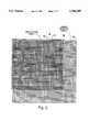
- FIG. 1is a perspective view of one embodiment of the flat-panel display test system in accordance with the invention.
- FIG. 2is a schematic diagram of one configuration of cameras and processing equipment incorporated in the test system
- FIG. 3illustrates a Moire pattern which typically results when a display image is detected by a camera incorporating a detector pixel array
- FIG. 4illustrates pixel groups of red, green, and blue pixels in a color display panel, wherein one color pixel within each pixel group is energized at a time during a test for brightness level and chromaticity of a color display panel;
- FIG. 5illustrates a color filter wheel incorporated in the test system for detecting brightness level and chromaticity of a color display panel
- FIG. 6is a graph of CIE spectral tristimulus values versus wavelength, used for determining chromaticity
- FIG. 7is a CIE chromaticity diagram used to plot tristimulus values in order to identify a resulting color
- FIG. 8is a schematic diagram of a configuration for conducting a viewing angle characterization test
- FIG. 9is a polar plot which may be generated in a viewing angle characterization test
- FIG. 10is a perspective view of an improved display panel connector, mounted on a hinged frame in the test system for FIG. 1, for interfacing a display panel to the test system;
- FIG. 11is an enlarged edge portion of a display panel and a connector, when the hinged frame is closed, showing an alignment circuit for aligning the connector to electrodes on the display panel.
- FIG. 1illustrates a flat-panel display test system 10 incorporating a variety of novel features.
- a flat-panel display 11, such as an LCD and the like, to be testedis positioned on a slidable table 12, and a hinged frame 14 (shown in more detail in FIG. 10) is then brought down to secure the display panel 11 in place.
- Slidable table 12which is typically an x-y stage allows easy positioning of the display panel 11 under a camera 15, such as a coupled CCD device camera and others.
- table 12is preferably movable in an x-y plane, by way of the x-y stage, and even a z-plane for precise positioning of the display.
- the x-y stagecan be any suitable base unit capable of moving the display panel in an x-direction and/or a y-direction.
- the stageincludes continuous movement in the x-direction and/or y-direction, at a high speed rate of about 20 mm/sec. to about 1.0 mm/sec., and includes a lower speed at about 1.0 mm/sec. to about 0.5 mm. sec. and less.
- the x-y stagealso increments at selected dimensions in the x-direction and the y-direction. The increment dimensions ranges from about 400 ⁇ m to about 5 ⁇ m a display pixel in the x-direction, and about 400 ⁇ m to about 5 ⁇ m in the y-direction.
- the x-y stagealso needs an accuracy (or tracking tolerance) of about ⁇ 5 ⁇ m and less in both the x-direction and the y-direction.
- accuracyor tracking tolerance
- exact increment dimensions in the x-direction and the y-directiondepend upon the particular application.
- a flexible ribbon type wire 16supplies drive signals from the pixel drive circuitry in test system 10 to conductors on hinged frame 14. Contact between the conductors on hinged frame 14 and the electrodes on the display panel 11 is made preferably automatic by the closing of hinged frame 14, to be discussed in more detail with reference to FIGS. 10 and 11.
- the high resolution camera 15is encased within an upper body 18 of test system 10, partially cut away to reveal camera 15.
- the camerais preferably an interline transfer CCD, with a 1.5K ⁇ 1.0K pixel array. Additional cameras may be used in conjunction with camera 15 to obtain the desired resolution and viewing angle.
- Camera 15, lens 20, and mirror 21are arranged so that the camera detects a complete image generated on display panel 11 when display panel 11 is appropriately positioned on table 12 and slid in place under camera 15.
- Camera 15, lens 20, and mirror 21are mounted on a movable support structure 22 for adjusting the height in a z-direction, and thus the field of view, of the camera 15.
- Support structure 22may also be movable in the horizontal direction such as an x-y direction if desired for a particular application.
- Features to the support structureare similar to the aforementioned x-y stage.
- a number of selectable color filters 23, including red, green, and blue tristimulus filters, on a filter wheel 24may be automatically rotated into place between lens 20 and the camera 15 aperture. These filters 23 will be discussed in more detail with respect to FIGS. 4-7.
- Test system 10also includes a second camera 25, which may be a CID camera, a charge coupled device (CCD) type camera or the like, for conducting viewing angle tests of display panel 11. Such a test is discussed in detail with respect to FIGS. 8 and 9.
- Camera 25is mounted on an x-y movable support structure 26 for positioning camera 25 over selected portions of display panel 11.
- a computer(not shown) and keyboard 27 are also incorporated into test system 10 to allow an operator to identify, via keyboard 27, various characteristics of the display panel or to select specific tests to be conducted.
- the computermay additionally be used to process image data or otherwise compile test data from a test.
- a computer monitor 28may display test parameters and/or the operating status of test system 10.
- a light source (not shown) encased within a lower body 30 of test system 10is used to provide any required back-lighting of the display panel 11.
- An example of such light sourcemay be triband phosphor cold cathode fluorescent lamp, and the like.
- a schematic diagram of one possible implementation of test system 10is shown in FIG. 2.
- the field of view of the high resolution CID camera 15covers the enter area of display panel 11. Additional cameras, in conjunction with camera 15, may be used if larger display panels are to be tested or if higher resolution is needed.
- the output of camera 15 on line 32is applied to an image processing computer 34, which may then appropriately process the camera 15 signals for evaluating the display image.
- Image processing computer 34is controlled by a computer 36, which interfaces with the operator using a monitor and keyboard 38.
- the brightness of a display panel pixelmay be acutely affected by the viewing angle.
- the signals outputted by the camera detector pixels on line 32 in FIG. 2may be compensated by digital techniques to remove any effects of viewing angle on the detected brightness levels of the display panel pixels.
- a test program for a specific type of display panelis programmed into computer 36 and automatically controls the test procedures, including applying signals to the display panel drivers 40.
- Conductors 41(shown as flexible ribbon 16 in FIG. 1) couples the driver output signals to the hinged cover 14, shown in FIG. 1, and ultimately to the electrodes on display panel 11.
- test data file 42The results of a test for each display panel are recorded in a test data file 42. This enables any trends in defects or non uniformity to be detected and corrected in the manufacturing process.
- a back-side light source 44is used for a light-blocking type LCD display panel placed on table 12. Displays in which the display pixels themselves emit photons may not require a backlight.
- a display panel 11 which is positioned on table 12 in FIGS. 1 or 2may either be a completed display, prior to its connection to a lap-top computer or the like, or may be a panel which is not completely fabricated. This enables the display manufacturer to save costs of further manufacture if the display panel could not be brought within specifications and enables the correction of certain defects in the display panel. Testing of such an incomplete display may also confirm specifications at various points in the manufacture of the display panel.
- the automatic test system 10may be programmed to conduct a display pixel brightness uniformity test and calculate necessary adjustments for each of the pixel driving voltages to correct for brightness nonuniformity.
- the testfirst determines the relative brightness of each of the pixels of a display panel.
- test system 10must apply voltages to the electrodes on the display panel to energize the pixels and display an image to be detected.
- itis necessary to eliminate the image distorting effects of aliasing that occur when display pixels are imaged onto a camera detector array having detector pixels which do not uniformly align with each of the pixels of the display panel.
- Aliasingis a well-known phenomena that may manifest itself as a Moire pattern (or interference pattern), which is a periodic modulation of an image voltage signal created by the camera array.
- the Moire phenomenonis due to the display pixels not being mapped onto the camera detecting pixels in exactly a one-to-one correspondence. If the mapping is not precisely a one-to-one correspondence, the photons associated with certain display pixels will fall onto non-sensitive portions (if any) of the camera array, and, conversely, the "streets and alleys" between the display pixels will be imaged onto sensitive areas of the camera array. The result of this less than optimal pixel relationship results in a Moire pattern, such as shown in FIG. 3, that distorts the true relative brightness levels of the display pixels.
- Test system 10employs a special multi-frame image translation technique to eliminate any inaccuracies in a detected image due to aliasing.
- FIG. 3illustrates a sample Moire pattern which may result from the focused display panel pixels 50 not being mapped in a one-to-one correspondence with the smaller and more densely populated camera detector pixels 52.
- certain of the camera detector pixels 52such as pixel 54
- pixel 54are completely superimposed by a single display panel pixel image 56. Consequently, these display panel pixels 56 completely superimposing a single camera detector pixel 54 will be detected by the camera detector pixels as being brighter than those display panel pixels, such as pixel 58, whose images partially fall on the nonsensitive areas between two adjacent camera detector pixels 52. Due to the Moire pattern of FIG. 3, if only a single display image were evaluated, the brightness of certain display panel pixels will be inaccurately detected as being brighter than other display panel pixels.
- a first inspection of the display panel pixelsis conducted at a first alignment of the display panel image and the camera pixel array, such as the alignment shown in FIG. 3.
- the brightness level (i.e., intensity) signal generated by each of the camera detector pixels 52 for this first alignmentis cross-referenced to a specific display pixel which gave rise to the brightness level signal and then mapped into a memory within computer 36 (FIG. 2). Suitable mapping techniques would be known to those skilled in the art.
- the display imageis slightly shifted relative to the camera detector pixels 52, such as by either physically shifting the display panel or camera(s) optics or by changing the angle of reflecting mirror 21 (FIG. 1). After this shifting, another image of the display panel is detected and mapped into memory.
- the Moire patternwill be slightly different than that shown in FIG. 3.
- the display panel imageis then shifted again relative to the camera detector pixels. This process is repeated until each of the display panel pixels has, during any of the detection stages, been detected by a camera detector pixel located entirely within an image of the display pixel.
- a camera detector pixelwhich is located entirely within a display pixel image (i.e., completely superimposed by the display pixel image) will detect an accurate relative brightness level of the display pixel.
- the number of required shifts of the display panel image with respect to the camera detector pixelsmay include four small incremental shifts to the left or right and four small incremental shifts up or down before the Moire pattern in FIG. 3 is repeated.
- the camerais displaced relative to a zero point on the display panel in a first x-direction at a distance x 1 , a second x-direction at a distance x 2 , a first y-direction at a distance y 1 , and a second y-direction at a distance y 2 .
- the distance x 2is equal to about the distance (-x 1 ) or 2y 1
- the distance y 2is equal to about the distance (-y 1 ) or 2y 1 .
- the required number of shifts and magnitude of the shiftswill be that needed to allow each of the display pixels to be detected by a camera detector pixels residing wholly within the projected image of the display pixel. A single map is then made of only those maximum intensity signals associated with each display pixel.
- This informationis then used to analyze the entire display.
- An alternative to first determining the maximum intensity ratio associated with each display pixel after all the incremental shifts and mapping these maximum intensities ratios into a single mapis to simply average, over all the incremental shifts, the brightness level output signals of a camera detector pixel receiving any portion of a corresponding display pixel image. This average intensity level for each display pixel over all the incremental shifts would then be mapped so that each display pixel would be associated with an accurate relative intensity level.
- the present methodalso employs use of several images to average out a periodic modulation of a Moire interference pattern.
- the present methodincludes a step of capturing from a display panel a first image which contains the periodic modulation.
- the first imageis captured by way of a CCD type camera or the like, and preferably stored into memory by way of standard mapping techniques.
- a step of displacing the CCD camera relative to the display panelis then performed.
- the display panelis displaced in an x-direction and/or a y-direction relative to the CCD camera array.
- the CCD camerais displaced in an x-direction and/or a y-direction relative to the panel.
- both the CCD camera and panelare displaced in x and/or y-directions to create a relative spatial displacement between each of them.
- the relative displacement between the CCD camera and the panelis preferably about one-half of a panel display pixel period in the x-direction when displacement occurs in the x-direction.
- the relative displacement between the CCD camera and the display panelis preferably about one-half of a panel display pixel period in the y-direction when displacement occurs in the y-direction.
- the relative spatial displacement between the CCD camera and the display panelis one-half of a panel display pixel period in the x or the y directions.
- the preferred embodimentalso includes a step of capturing (or acquiring) a second image of the display panel, and storing such second image into memory also by way of standard mapping techniques.
- the second imagealso contains the same periodic modulation with the same period as the first image. But the placement of the periodic modulation of the second image will be displaced by one-half of a period in either the x-direction or the y-direction relative to the first image by way of the displacing step. Of course, the placement of the periodic modulation cannot be positioned onto another display pixel at the same relative location of the display pixel in the first image acquisition step.
- a step of adding the first and second images to one anotherare then performed by use of standard image processing techniques.
- the periodic patternseffectively cancel each other out and the "real" modulations in the panel are preserved.
- Any number of imagescan be added together as long as they meet the following criteria.
- the number of imagesis at least two, and more preferably the number of images is two and greater, and more preferably the number of images is four and greater.
- the camerais displaced relative to a zero point on the display panel in a first x-direction at a distance x 1 , a second x-direction at a distance x 2 , a first y-direction at a distance y 1 , and a second y-direction at a distance y 2 .
- the distance x 2is equal to about the distance (-x 1 ) or 2x 1
- the distance y 2is equal to about the distance (-y 1 ) or 2y 1 .
- Each image that is acquiredmust have a matching image (or complementary image) with a relative displacement of one-half a panel pixel period in the x-direction or the y-direction, or both the x and y directions.
- the cameramay be displaced in the y-direction before the x-direction, or a combination thereof.
- the present inventionprovides a method for reducing and even eliminating a periodic modulation from a display panel image signal by way of filtering.
- the present methodincludes a step of filtering a modulated signal by way of a spatial filter from the display panel image signal.
- a period of the modulated signalis determined from a period of the display panel pixels and a period of the CCD pixels in spatial domain.
- An image processor(and computer) performs a spatial filter onto the display panel image signal by convolving the CCD signal with a filter of a width designed to remove the periodic modulation.
- the CCD signalfrom spatial domain to a frequency domain using a techniques such as a Fourier Transform and the like.
- a frequency of the Moire interference patterncan be calculated from the period of the CCD pixels and FPD pixels. Techniques such as bandpass filtering and the like can be used to remove selected frequencies which include the Moire interference pattern.
- a preferred next stepis to analyze the brightness uniformity across the display panel and then take steps to correct for any brightness nonuniformity. In one embodiment, this is accomplished by detecting the minimum display pixel brightness level and using that minimum brightness as a baseline for the correction of all other display pixel brightnesses. Compensation factors are then calculated for each of the display pixel driving voltages.
- These compensation factorsare then loaded into a look-up table in memory, located in computer 36 in FIG. 2. These factors in the look-up table may then be applied to the display drivers, via a compensation control circuit 64 in FIG. 2, to lower the drive voltages for those pixels whose brightness levels need to be attenuated to match that of the minimum brightness pixel.
- the displayed imageis then detected again using the same process described above, and the brightness levels are again measured to determine any nonuniformity. This process for correcting the brightness uniformity may be reiterated until the desired brightness uniformity is established.
- This alternative process of determining brightness uniformitywould be conducted for each shifted position of the display image relative to the camera detector pixels.
- the selected pixels in the display to be adjusted for each image shiftwould be only those identified as having an image completely superimposing a single camera detector pixel to avoid the effects of the Moire phenomenon illustrated in FIG. 3. After all the image shifts, all the display pixels should have a predetermined same brightness level.
- a pixel darkness levelmay be substituted for a pixel brightness level depending on if the display pixels scatter light or if the display pixels themselves emit light.
- the final compensation factors for each of the display pixelsmay then be down-loaded into an EPROM chip 66 (FIG. 2) for that particular display panel tested.
- the EPROM 66would then be disconnected from test system 10 and installed in a drive system for that particular display panel to permanently control the compensation of the display driver signals to achieve a uniform brightness across the display panel.
- an energizing pixel voltagemay also affect at what angle the pixel element seems brightest (or darkest).
- the above brightness uniformity testmay also be used to cause the display pixels to have the greatest uniform contrast ratio (ratio of brightness to darkness) rather than simply to set a brightness level at a baseline level.
- ratio of brightness to darknessratio of brightness to darkness
- Pixel defects and other defectsin the display panel may be simply detected by detecting a pixel brightness level below a threshold value. Such defects may be identified by test system 10 and fixed or, alternatively, the display panel may be discarded. To enable such fixing of defects, it is recommended to test the display panel during a manufacturing stage where its pixel elements and conductors are exposed.
- the test system 10may include a special camera and/or zoom lens which can automatically be directed by test system 10 to any defective display portion, and the defective portion may be photographed to aid in the correction of the defect.
- Methods of correction of a defect in a display panelare described in copending U.S. application Ser. No. 07/716,592, assigned to the present assignee.
- color filters 23 in FIG. 1are used to detect the brightness levels and chromaticity of the red, green, and blue display panel pixels.
- red pixels 70To detect brightness uniformity across a color display panel having individually energizable red (R), green (G), and blue (B) pixels, as illustrated in FIG. 4, a single color of pixels is energized at a time. For example, with reference to FIG. 4, only red pixels 70 would be initially energized in the display panel 72.
- the filter wheel 24 in FIG. 1is shown in more detail in FIG. 5.
- the filter wheel 24When detecting the brightness (not chromaticity) of the red pixels 70 in FIG. 4, the filter wheel 24 is positioned so that a narrow bandpass red filter 74 will be interposed between the camera lens 20 and the camera 15 aperture.
- the image across the displayis detected using the incremental shifting techniques previously described to avoid aliasing effects. Since, in color displays, each display pixel imaged onto the camera detector pixel array will generally be smaller than a single detector pixel, the signal-to-noise (S/N) ratio of each color display pixel will be relatively small.
- an average intensity value outputted by the camera detector pixelsis taken after a predetermined number of incremented shifts. (This is in contrast to mapping only a minimum pixel intensity for a single shift, as previously described.) This average value will then be mapped into a memory and will accurately reflect the relative brightness of the red pixels in the color display.
- Any brightness non-uniformitiescan be corrected using the methods previously described with respect to FIG. 2. Pixel defects may also be identified.
- the processis then repeated for the blue pixels being filtered by the blue filter 78 in FIG. 5.
- the brightness levels of the red, green, and blue pixels in a color displaycan be accurately measured, without the effects of aliasing, and corrected, if necessary, using test system 10.
- the filter wheel 24 in FIG. 5may be set so that the opening 80 is between the lens 20 and the camera 15 aperture.
- a second filter wheelmay be located in front of filter wheel 24 to provide neutral density filters (e.g., shades of gray) to attenuate light from high brightness display panels.
- neutral density filterse.g., shades of gray
- tristimulus filters 82, 84, 86, and 88are used to modify the camera's 15 spectral response to match the CIE Colorimetric System tristimulus spectral response for each of the four primary stimuli curves x( ⁇ ) 90,92, y( ⁇ ) 94, and z( ⁇ ) 96 shown in FIG. 6.
- the tristimulus spectral responses shown in FIG. 6take into account the sensitivity of a human eye to the various wavelengths of light.
- This chromaticity test conducted by test system 10determines the quality or pureness of the red, green, and blue emitted by the red, green, and blue pixels in a color display panel.
- any displayed colormay be defined by its detected tristimulus values.
- the output of the camera 15may correspond to a tristimulus value of 0.5 when using x( ⁇ ) filter 82, correspond to a tristimulus value of 0.2 when using y( ⁇ ) filter 86, and correspond to a value of zero when using x( ⁇ ) filter 84 and z( ⁇ ) filter 88.
- xis calculated to be approximately 0.71
- yis calculated to be approximately 0.28
- zis calculated to be zero.
- chromaticity coordinatesmay then be plotted as point 97 on the x-y CIE chromaticity diagram in FIG. 7 to reveal that such a displayed red color image by one or more pixels in the color display panel under test is virtually pure red.
- a range of wavelengthswill be emitted by a color display panel pixel, and such a range may be depicted as a small circle or an ellipse when plotted on the diagram of FIG. 7. The location and size of this circle or ellipse will determine the quality of the displayed pixel image.
- the determination of tristimulus values and the plotting of coordinates on the diagram of FIG. 7have been described with respect to mental calculations and manual plotting, the determination of these values and their characterization is performed by software in test system 10. If desired, a plot as shown in FIG. 7 may actually be printed by the test system 10 for a single pixel or for the entire display panel. Otherwise, a simple rating of the color display may be provided by the test system 10.
- the above-described process used for determining the pureness of red emitted by the red pixels in the display being testedis then conducted for the green pixels and the blue pixels in the color display panel, and a similar analysis is performed to determine the quality of the green and blue display qualities of the color display panel.
- the quality of color output of each individual pixel in the color display panelmay be mapped in a memory of computer 36 (FIG. 2).
- the mapped datacan be compared to any manufacturer's specifications for color to determine the quality of each of the pixels in the color display panel. Such a determination of color quality may be for each pixel or for selected portions of the display or for the entire display.
- the tristimulus filters 82, 84, 86, 88are absorptive type and the filter material is optical quality glass.
- the filtersare manufactured using optical fabrication techniques and tolerances.
- each of the four tristimulus filters 82, 84, 86, 88is a lamination of several different filter glasses with different thicknesses and spectral transmissions. For rays passing through the filters at non-normal incidence, the transmission of an absorptive filter will change due to an increase in the optical path length.
- test system 10Another test which may be conducted by test system 10, especially for LCD panels, is a viewing angle characterization test.
- the effective viewing angle for an image displayed on an LCD panelis relatively limited and may influence the usefulness of the LCD panel.
- a conventional electronic method to detect the viewing angle of a display panelis to move the angle of a detector (which may be a human eye) relative to the display panel to detect where the brightness level of an image falls to a certain percentage of the maximum brightness.
- FIG. 8illustrates an improved viewing angle characterization method carried out by the automatic test system 10 in FIG. 1.
- a single pixel 100is energized in a display panel 102.
- a lens 104 on camera 25 in FIG. 1is used to focus substantially all light emanating from pixel 100 onto a camera pixel array 108.
- lens 104comprises two infinity corrected microscope objective lenses, positioned back-to-back, so that the image of the pixel 100 can be placed closer to the camera pixel array 108. If the panel 102 were a reflective type LCD, lens 104 would be used to focus the effective darkness "emanating" from pixel 100, and a light source would be mounted either above the LCD or under the LCD. A field stop 110 is used to limit the field of view to only that angle sufficient to measure the viewing angle of pixel 100.
- the pixel imageis then focused on camera pixel array 108, and each pixel within array 108 outputs a signal corresponding to the detected brightness of the pixel image. While pixel array 108 is fixed relative to pixel 100, virtually the entire pixel array 108 area is used to directly map the brightness level versus viewing angle of the single display pixel 100. No interference patterns are required to be generated using this method.
- the maximum brightness levelgenerally located at a central portion of array 108, may then be compared to the other brightness levels detected around the array 108 to determine where in array 108 the brightness level falls off to, for example, 50% of the maximum brightness.
- a computersuch as computer 36 in FIG. 2, in combination with an imaging processor 34, then effectively generates a polar plot, such as shown in FIG. 9, of the brightness level versus viewing angle for the single pixel 100.
- the polar plotmay then be stored in test data file 42 and/or printed to enable one to visually examine the brightness level versus viewing angle.
- a predetermined criteria for the viewing anglemay be compared by the computer with the internally generated polar plot, and the viewing angle may be simply identified to the operator as pass/fail.
- a number of individual pixels 100 around the display panel 102 in FIG. 8are measured to obtain a representative viewing angle for selected areas over the display panel 102. This may be used to approximate the viewing angle of the entire display panel 102 and to generate a polar plot of the entire display.
- FIGS. 1 and 8Other lens and camera arrangements may be used instead of the configuration of FIGS. 1 and 8, such as placing camera array 108 sufficiently close to pixel 100 so as to eliminate the need for lens 104 or to use reflector optics rather than refractive optics. Other optical arrangements would be obvious to those of ordinary skill in the art.
- test system 10incorporates a novel display panel connector 120 (FIG. 10) whose electrical contacts may be quickly and reliably pressed onto the electrodes of a display panel during testing. It has been found very difficult in the past to quickly and reliably connect the many finely pitched thin metal-film contacts around the perimeter of the display panel to electrodes of a test system.
- FIG. 10illustrates an LCD array 122 with finely pitched metal film electrodes 124 arranged around its periphery for coupling electrical signals to the various pixel elements forming the LCD array.
- An enlargement of an edge portion of LCD 122 within circle 126illustrates in more detail the metal film electrodes 124.
- a pixel in the LCD array 122is energized by energizing a specific row line and column line in the array 122 terminating in an associated electrode 124.
- electrodes 124are formed on glass, where such electrodes 124 may have a pitch (distance between the centers of adjacent electrodes) of 1/10,000th of an inch. In a conventional test system, alignment of the LCD electrodes 124 with a test system connector would normally be done manually.
- connector 120is provided on a bottom surface of hinged frame 14 (also shown in FIG. 1).
- One form of connector 120is shown in detail in FIG. 10 within circle 130, where a flexible tape 132 has metal traces 134 formed thereon corresponding to a group of thin film electrodes 124 shown within circle 126.
- a flexible tape 132may be formed of a polymer tape, such as KaptonTM, having traces 134 formed on it using a conventional metal deposition and photolithographic etching processes. Traces 134 are connected to a flexible wire 138 leading to display drivers 40 (FIG. 2) for LCD panel 122.
- the traces 134 on connector 120correspond to an electrode 134 pattern configured for the specific display panel 122 to be tested.
- LCD panel 122is positioned against a block 140, or other reference position, formed on table 12 of test system 10 so that the position of LCD panel 122 and the position of electrodes 124 will be predetermined.
- Connector 120is either prepositioned with respect to block 140, or automatically or manually positioned with respect to block 140, so that the flexible circuit traces 134 align with the respective ones of electrodes 124 on LCD panel 122.
- the resilience of tape 132ensures adequate pressure will be applied to each of electrodes 124.
- table 12may include a photodetector 144 which senses the overlapping of a first electrode 124 on LCD panel 122 and a respective trace 134 on flexible tape 132.
- a light emitting diode 146is located in table 12 under transparent LCD panel 122.
- Flexible tape 132is made transparent or semi-transparent so that the amount of light received by photodetector 144 is a maximum when trace 134 and electrode 124 overlap.
- the conductivity of photodetector 144may then be used to automatically shift block 140 in FIG. 10 to shift LCD panel 122 with respect to connector 120 so as to obtain a maximum output signal from photodetector 144.
- the positions of photodetector 144 and LED 146are reversed.
- an improved automatic test system for a flat-panel displayhas been described above which eliminates problems due to aliasing and Moire patterns, and which accurately detects and corrects for brightness uniformity, color quality, and viewing angle for a flat-panel display.
- test system 10with any type of display panel repair system, such as that described in U.S. Pat. No. 5,235,272, entitled “Method and Apparatus for Automatically Inspecting and Repairing an Active Matrix LCD Panel” to automatically repair any identified defective pixel.
- display panel repair systemsuch as that described in U.S. Pat. No. 5,235,272, entitled “Method and Apparatus for Automatically Inspecting and Repairing an Active Matrix LCD Panel” to automatically repair any identified defective pixel.
- an automatic testing and repair systemis also envisioned by this disclosure.
Landscapes
- Engineering & Computer Science (AREA)
- Theoretical Computer Science (AREA)
- Physics & Mathematics (AREA)
- Computer Hardware Design (AREA)
- General Physics & Mathematics (AREA)
- General Engineering & Computer Science (AREA)
- Quality & Reliability (AREA)
- Testing Of Optical Devices Or Fibers (AREA)
- Liquid Crystal Display Device Control (AREA)
Abstract
Description
Claims (20)
Priority Applications (3)
| Application Number | Priority Date | Filing Date | Title |
|---|---|---|---|
| US08/394,668US5764209A (en) | 1992-03-16 | 1995-02-22 | Flat panel display inspection system |
| JP05821996AJP3245731B2 (en) | 1995-02-22 | 1996-02-22 | Flat panel display inspection system |
| KR1019960004558AKR100397080B1 (en) | 1995-02-22 | 1996-02-22 | Flat Display Inspection System |
Applications Claiming Priority (2)
| Application Number | Priority Date | Filing Date | Title |
|---|---|---|---|
| US85245892A | 1992-03-16 | 1992-03-16 | |
| US08/394,668US5764209A (en) | 1992-03-16 | 1995-02-22 | Flat panel display inspection system |
Related Parent Applications (1)
| Application Number | Title | Priority Date | Filing Date |
|---|---|---|---|
| US85245892AContinuation-In-Part | 1992-03-16 | 1992-03-16 |
Publications (1)
| Publication Number | Publication Date |
|---|---|
| US5764209Atrue US5764209A (en) | 1998-06-09 |
Family
ID=46202576
Family Applications (1)
| Application Number | Title | Priority Date | Filing Date |
|---|---|---|---|
| US08/394,668Expired - Fee RelatedUS5764209A (en) | 1992-03-16 | 1995-02-22 | Flat panel display inspection system |
Country Status (1)
| Country | Link |
|---|---|
| US (1) | US5764209A (en) |
Cited By (94)
| Publication number | Priority date | Publication date | Assignee | Title |
|---|---|---|---|---|
| WO1999013322A1 (en)* | 1997-09-08 | 1999-03-18 | Photon Dynamics, Inc. | Color filter inspection method and apparatus |
| US5966458A (en)* | 1996-06-28 | 1999-10-12 | Matsushita Electric Industrial Co., Ltd. | Display screen inspection method |
| US5987624A (en)* | 1997-06-10 | 1999-11-16 | Paradise Electronics, Inc. | Method and apparatus for automatically determining signal parameters of an analog display signal received by a display unit of a computer system |
| US6292157B1 (en)* | 1996-03-25 | 2001-09-18 | Rainbow Displays, Inc. | Flat-panel display assembled from pre-sorted tiles having matching color characteristics and color correction capability |
| US20010048529A1 (en)* | 2000-05-31 | 2001-12-06 | Fotland Richard A. | Method of image color correction |
| US20020000983A1 (en)* | 2000-05-19 | 2002-01-03 | Lg. Philips Lcd Co., Ltd. | Method for examining quality of flat panel display device |
| WO2002039130A1 (en)* | 2000-11-09 | 2002-05-16 | Display Products Technology Limited | Method and apparatus for testing flat panel video displays |
| US6417686B1 (en) | 1996-11-14 | 2002-07-09 | Si Diamond Technology, Inc. | Display panel test device |
| US6466882B1 (en)* | 1998-08-21 | 2002-10-15 | Samsung Electronics Co., Ltd. | Integrated system for detecting and repairing semiconductor defects and a method for controlling the same |
| US20020157033A1 (en)* | 2000-11-01 | 2002-10-24 | Nokia Corporation | Testing an image display device |
| US6498592B1 (en) | 1999-02-16 | 2002-12-24 | Sarnoff Corp. | Display tile structure using organic light emitting materials |
| US6501451B1 (en)* | 1997-10-23 | 2002-12-31 | Canon Kabushiki Kaisha | Liquid crystal display panel driving device and method |
| US20030055591A1 (en)* | 2001-09-14 | 2003-03-20 | American Panel Corporation | Visual display testing, optimization, and harmonization method and system |
| US20030059101A1 (en)* | 2001-07-05 | 2003-03-27 | Photon Dynamics, Inc. | Moire suppression method and apparatus |
| US20030112331A1 (en)* | 2001-12-17 | 2003-06-19 | Hannstar Display Corp. | Positioning and inspecting system and method using same |
| US6590643B2 (en)* | 2000-03-28 | 2003-07-08 | Japan Science And Technology Corporation | Method and apparatus for measuring viewing angle characteristic and positional characteristic of luminance |
| US6606116B1 (en)* | 2000-03-30 | 2003-08-12 | Ncr Corporation | Methods and apparatus for assessing quality of information displays |
| US6670953B1 (en)* | 1998-10-16 | 2003-12-30 | Seiko Epson Corporation | Electro-optical device substrate, active matrix substrate and method for inspecting electro-optical device substrate |
| US20040041977A1 (en)* | 2002-08-26 | 2004-03-04 | Chien-Ching Shen | Method and device for repairing defective pixels of a liquid crystal display panel |
| US6714670B1 (en)* | 1998-05-20 | 2004-03-30 | Cognex Corporation | Methods and apparatuses to determine the state of elements |
| US6727864B1 (en)* | 2000-07-13 | 2004-04-27 | Honeywell International Inc. | Method and apparatus for an optical function generator for seamless tiled displays |
| KR20040045173A (en)* | 2002-11-22 | 2004-06-01 | 갈란트 프리시젼 머시닝 캄파니, 리미티드 | Inspection system with alternation pallets |
| US20040104919A1 (en)* | 2000-08-25 | 2004-06-03 | International Business Machines Corporation | Brightness controlling apparatus, brightness adjusting system, computer system, liquid crystal display unit, brightness controlling method, computer software, and storage medium |
| US20040109158A1 (en)* | 2002-11-29 | 2004-06-10 | Chang-Chih Sung | Light guide plate measurement apparatus |
| US20040114198A1 (en)* | 2002-12-16 | 2004-06-17 | Samsung Electronics Co., Ltd. | Image processing system and method |
| US6760471B1 (en)* | 2000-06-23 | 2004-07-06 | Teradyne, Inc. | Compensation system and related techniques for use in a printed circuit board inspection system |
| FR2854300A1 (en)* | 2003-04-25 | 2004-10-29 | Johnson Contr Automotive Elect | FLAT DISPLAY DEVICE AND ADJUSTMENT SYSTEM FOR SUCH A DEVICE. |
| US20040227697A1 (en)* | 2003-05-14 | 2004-11-18 | Canon Kabushiki Kaisha | Signal processing apparatus, signal processing method, correction value generation apparatus, correction value generation method, and display apparatus manufacturing method |
| US20040263497A1 (en)* | 2001-12-17 | 2004-12-30 | Thierry Leroux | Low resolution acquisition method and device for controlling a display screen |
| US20050007364A1 (en)* | 2001-08-27 | 2005-01-13 | Yoshifumi Oyama | Method for sorting ununiformity of liquid crystal display panel sorting apparatus, and information recorded medium with recorded program for executing this sorting |
| US20050037735A1 (en)* | 2003-07-31 | 2005-02-17 | Ncr Corporation | Mobile applications |
| US20050078104A1 (en)* | 1998-02-17 | 2005-04-14 | Matthies Dennis Lee | Tiled electronic display structure |
| US20050099631A1 (en)* | 2002-12-26 | 2005-05-12 | Ming-Feng Yu | Ambient temperature control apparatus used for measuring display panel |
| US20050190165A1 (en)* | 2002-10-02 | 2005-09-01 | Philippe Wendling | Display panels, display units and data processing assemblies |
| US6954193B1 (en)* | 2000-09-08 | 2005-10-11 | Apple Computer, Inc. | Method and apparatus for correcting pixel level intensity variation |
| US20050232476A1 (en)* | 2004-04-19 | 2005-10-20 | Semiconductor Energy Laboratory Co., Ltd. | Image analysis method, image analysis program and pixel evaluation system having the sames |
| US20050263674A1 (en)* | 2004-05-27 | 2005-12-01 | Joon-Chok Lee | Method and apparatus for adjusting a mixed light produced by first and second light sources of first and second colors |
| US20060017676A1 (en)* | 2004-07-23 | 2006-01-26 | Bowers Gerald M | Large substrate flat panel inspection system |
| US7064768B1 (en)* | 2002-03-20 | 2006-06-20 | Ess Technology, Inc. | Bad pixel correction while preserving features |
| US20060139269A1 (en)* | 2004-12-24 | 2006-06-29 | Samsung Electronics Co., Ltd. | Apparatus for measuring response time and method of measuring response time using the same |
| US20060158643A1 (en)* | 2004-12-13 | 2006-07-20 | Hoya Corporation | Method and system of inspecting mura-defect and method of fabricating photomask |
| EP1724744A1 (en)* | 2005-05-20 | 2006-11-22 | Seiko Epson Corporation | Test probe and manufacturing method for test probe |
| US20060285025A1 (en)* | 2005-06-15 | 2006-12-21 | Seiko Epson Corporation | Image display device and method |
| US20070041112A1 (en)* | 2005-08-17 | 2007-02-22 | Browning William T | Laptop computer screen night vision apparatus |
| US20070058044A1 (en)* | 2005-09-09 | 2007-03-15 | Radiant Imaging, Inc. | Systems and methods for measuring spatial and angular performance of a visual display |
| CN1312654C (en)* | 2003-01-10 | 2007-04-25 | 夏普株式会社 | Display device, drive circuit, checking device, recording medium |
| US20070132895A1 (en)* | 2005-12-12 | 2007-06-14 | Novatek Microelectronics Corp. | Compensation device for non-uniform regions in flat panel display and method thereof |
| US20070229814A1 (en)* | 2006-03-31 | 2007-10-04 | Hoya Corporation | Pattern defect inspection method, photomask manufacturing method, and display device substrate manufacturing method |
| US20070281734A1 (en)* | 2006-05-25 | 2007-12-06 | Yoram Mizrachi | Method, system and apparatus for handset screen analysis |
| US20080030524A1 (en)* | 2006-06-30 | 2008-02-07 | Kabushiki Kaisha Toshiba | Method and apparatus for imaging display panel and method for manufacturing display panel |
| US20080030725A1 (en)* | 2006-08-02 | 2008-02-07 | Fujitsu Limited | Display panel inspection apparatus and method |
| US20080049051A1 (en)* | 2006-07-28 | 2008-02-28 | Han Sang C | Method of controlling picture quality in flat panel display |
| US20080063254A1 (en)* | 2006-09-07 | 2008-03-13 | Kabushiki Kaisha Toshiba | Unevenness inspection method, method for manufacturing display panel, and unevenness inspection apparatus |
| US20080111805A1 (en)* | 2006-11-10 | 2008-05-15 | Innolux Display Corp. | Liquid crystal display having common voltage initialization circuit and method for manufacturing same |
| US20080158241A1 (en)* | 2007-01-02 | 2008-07-03 | Samsung Sdi Co., Ltd. | Method of optimizing brightness of liquid crystal display panel |
| US20080278421A1 (en)* | 2007-05-11 | 2008-11-13 | Sony Corporation | Method for uneven light emission correction of organic el panel and display correction circuit of organic el panel |
| US20090175530A1 (en)* | 2007-11-12 | 2009-07-09 | Fredrik Sjostrom | Methods and apparatuses for detecting pattern errors |
| US20090322664A1 (en)* | 2008-06-27 | 2009-12-31 | American Panel Corporation | System and method for optimizing LCD displays |
| US20100013750A1 (en)* | 2008-07-18 | 2010-01-21 | Sharp Laboratories Of America, Inc. | Correction of visible mura distortions in displays using filtered mura reduction and backlight control |
| US20100039639A1 (en)* | 2006-08-09 | 2010-02-18 | Research In Motion Limited | Device and system for evaluating a lens for an electronic device |
| CN1773301B (en)* | 2004-11-11 | 2010-10-20 | 三星电子株式会社 | Inspection device for display panel and inspection method for the inspection device for display panel |
| US20100328653A1 (en)* | 2009-06-24 | 2010-12-30 | Chunghwa Picture Tubes, Ltd. | Method and system of evaluating a stereo image displaying panel |
| US20110185322A1 (en)* | 2010-01-25 | 2011-07-28 | Palo Alto Research Center Incorporated | Method of in-process intralayer yield detection, interlayer shunt detection and correction |
| TWI383141B (en)* | 2008-04-22 | 2013-01-21 | Shuz Tung Machinery Ind Co Ltd | Panel inspection apparatus |
| US20130329057A1 (en)* | 2012-06-08 | 2013-12-12 | Apple Inc. | Systems and Methods for Dynamic Dwelling Time for Tuning Display to Reduce or Eliminate Mura Artifact |
| CN103559857A (en)* | 2013-10-31 | 2014-02-05 | 桂林机床电器有限公司 | Method and device for OLED screen pixel defect detection |
| US20140049778A1 (en)* | 2012-08-16 | 2014-02-20 | Beijing Boe Display Technology Co., Ltd. | Device And A Method For Detecting A Transmittivity Spectrum Of A Light Guiding Plate |
| US8912483B2 (en) | 2012-12-26 | 2014-12-16 | Industrial Technology Research Institute | Display measuring device |
| US9070316B2 (en) | 2004-10-25 | 2015-06-30 | Barco Nv | Optical correction for high uniformity panel lights |
| US20160084683A1 (en)* | 2014-09-19 | 2016-03-24 | Apple Inc. | In store display calibration system |
| EP2957102A4 (en)* | 2013-02-18 | 2016-11-02 | Kateeva Inc | QUALITY ASSESSMENT OF OLED STACK FILMS |
| US20160356812A1 (en)* | 2015-06-05 | 2016-12-08 | Boe Technology Group Co., Ltd. | Display panel testing bench |
| US20170140685A1 (en)* | 2014-12-31 | 2017-05-18 | Shenzhen China Star Optoelectronics Technology Co., Ltd. | Method of monitoring quality of liquid crystal display panel |
| US20170205277A1 (en)* | 2016-01-19 | 2017-07-20 | Mitsubishi Electric Corporation | Uneven brightness measuring apparatus |
| EP3171588A4 (en)* | 2014-07-15 | 2018-01-17 | IIX, Inc. | Image processing method and image processing apparatus executing that image processing method |
| US9898954B2 (en)* | 2015-07-22 | 2018-02-20 | Shenzhen China Star Optoelectronics Technology Co., Ltd | Liquid crystal panel common electrode voltage adjustment device and liquid crystal panel common electrode voltage adjustment method |
| EP3413293A1 (en)* | 2017-06-06 | 2018-12-12 | Vestel Elektronik Sanayi ve Ticaret A.S. | A light source arrangement and method of manufacturing a display device |
| US10156931B2 (en) | 2005-09-08 | 2018-12-18 | Power2B, Inc. | Displays and information input devices |
| US20190050619A1 (en)* | 2017-08-09 | 2019-02-14 | Synaptics Incorporated | Providing test patterns for sensor calibration |
| US10248229B2 (en) | 2004-04-01 | 2019-04-02 | Power2B, Inc. | Control apparatus |
| WO2019106636A1 (en)* | 2017-12-03 | 2019-06-06 | Lumus Ltd. | Optical device testing method and apparatus |
| US10339881B1 (en)* | 2017-12-28 | 2019-07-02 | Shenzhen China Star Optoelectronics Technology Co., Ltd. | Method of acquiring overdrive look-up table of liquid crystal display |
| US10452207B2 (en) | 2005-05-18 | 2019-10-22 | Power2B, Inc. | Displays and information input devices |
| US10459039B1 (en) | 2018-04-23 | 2019-10-29 | Capital One Services, Llc | Systems and methods for testing multi-element lighted displays |
| CN110428762A (en)* | 2019-07-10 | 2019-11-08 | 武汉精立电子技术有限公司 | Oled panel burn-in test characteristics of luminescence detection method based on pixel brightness |
| US10534496B2 (en) | 2007-03-14 | 2020-01-14 | Power2B, Inc. | Interactive devices |
| US10664070B2 (en) | 2002-06-08 | 2020-05-26 | Power2B, Inc. | Input system for controlling electronic device |
| US10970825B2 (en) | 2017-02-09 | 2021-04-06 | Iix Inc. | Image processing method and image processing apparatus for executing image processing method |
| CN112748118A (en)* | 2020-12-29 | 2021-05-04 | 乐金显示光电科技(中国)有限公司 | Detection system and detection method for display panel |
| US11335222B2 (en) | 2017-06-22 | 2022-05-17 | Photon Dynamics, Inc. | Method for detecting defects in ultra-high resolution panels |
| CN115273732A (en)* | 2022-06-13 | 2022-11-01 | 浙江大华技术股份有限公司 | Abnormal texture suppression method for display screen, terminal and computer-readable storage medium |
| WO2023200728A1 (en)* | 2022-04-11 | 2023-10-19 | Magik Eye Inc. | Calibrating a three-dimensional sensor |
| CN119618577A (en)* | 2025-02-12 | 2025-03-14 | 福建越华晖实业有限公司 | A viewing angle test device for LCD display production |
| US12387297B2 (en)* | 2020-07-17 | 2025-08-12 | TechnoTeam Holding GmbH | Method and device for reducing aliasing errors in images of pixel-based display devices and for the evaluation of display devices of this type |
Citations (25)
| Publication number | Priority date | Publication date | Assignee | Title |
|---|---|---|---|---|
| US2809232A (en)* | 1952-11-17 | 1957-10-08 | Stedman B Hoar | Television camera color attachment |
| US3718842A (en)* | 1972-04-21 | 1973-02-27 | Texas Instruments Inc | Liquid crystal display mounting structure |
| US4242703A (en)* | 1978-11-02 | 1980-12-30 | Olympus Optical Co., Ltd. | Projection apparatus for optical systems |
| US4400731A (en)* | 1980-03-06 | 1983-08-23 | Smiths Industries Public Limited Company | Testing display systems |
| US4491868A (en)* | 1981-05-06 | 1985-01-01 | Inspection Technology Inc. | Video image compensator for inspection apparatus |
| US4533950A (en)* | 1983-03-23 | 1985-08-06 | Visual Information Institute, Inc. | Method of testing the linearity of a raster scan |
| US4899105A (en)* | 1987-09-02 | 1990-02-06 | Tokyo Electron Limited | Method of testing electrical characteristics of LCD with probe device |
| US4922309A (en)* | 1987-11-09 | 1990-05-01 | Otsuka Electronics Co., Ltd. | Spectroscope |
| US4987032A (en)* | 1987-06-26 | 1991-01-22 | Fuji Photo Film Co., Ltd. | Functional organic thin film and method of manufacture thereof |
| US5015094A (en)* | 1988-10-03 | 1991-05-14 | Otsuka Electronics Co., Ltd. | Particle size measuring system |
| US5057695A (en)* | 1988-12-19 | 1991-10-15 | Otsuka Electronics Co., Ltd. | Method of and apparatus for measuring the inside information of substance with the use of light scattering |
| US5111110A (en)* | 1989-05-24 | 1992-05-05 | U.S. Philips Corporation | Method of determining a display parameter in a picture display tube and method of improving a picture display in a picture display tube |
| US5113083A (en)* | 1988-07-25 | 1992-05-12 | Otsuka Electronics Co., Ltd. | Light scattering measuring apparatus utilizing a photodetector mounted on a rotary stand |
| GB2254144A (en)* | 1991-03-27 | 1992-09-30 | Otsuka Denshi Kk | Three-angle polarisation analyser |
| US5169672A (en)* | 1990-01-30 | 1992-12-08 | Idemitsu Kosan Co., Ltd. | Process for producing thin films and color filters |
| JPH0527704A (en)* | 1991-02-04 | 1993-02-05 | Minato Electron Kk | Display screen reading method |
| US5216504A (en)* | 1991-09-25 | 1993-06-01 | Display Laboratories, Inc. | Automatic precision video monitor alignment system |
| US5239365A (en)* | 1991-04-03 | 1993-08-24 | Otsuka Electronics Co., Ltd. | Method of measuring thickness of liquid crystal cells |
| US5245326A (en)* | 1991-08-19 | 1993-09-14 | International Business Machines Corp. | Calibration apparatus for brightness controls of digitally operated liquid crystal display system |
| US5293178A (en)* | 1991-06-27 | 1994-03-08 | Matsushita Electric Industrial Co., Ltd. | Display screen inspecting apparatus |
| US5326729A (en)* | 1992-02-07 | 1994-07-05 | Asahi Glass Company Ltd. | Transparent quartz glass and process for its production |
| US5333610A (en)* | 1991-03-27 | 1994-08-02 | Otsuka Electronics Co., Ltd. | Absorption spectrum determining method and spectrometric measuring apparatus for light-diffusive object using the method |
| US5339093A (en)* | 1990-12-04 | 1994-08-16 | Ezel, Inc. | Liquid crystal panel inspection method |
| US5444329A (en)* | 1992-11-06 | 1995-08-22 | Kabushiki Kaisha Toshiba | Antireflection film and display apparatus comprising the same |
| US5450220A (en)* | 1992-09-30 | 1995-09-12 | Sharp Kabushiki Kaisha | Polymer dispersed liquid crystal with polymer glass transition above 50° C. and low isotropic transition shift |
- 1995
- 1995-02-22USUS08/394,668patent/US5764209A/ennot_activeExpired - Fee Related
Patent Citations (25)
| Publication number | Priority date | Publication date | Assignee | Title |
|---|---|---|---|---|
| US2809232A (en)* | 1952-11-17 | 1957-10-08 | Stedman B Hoar | Television camera color attachment |
| US3718842A (en)* | 1972-04-21 | 1973-02-27 | Texas Instruments Inc | Liquid crystal display mounting structure |
| US4242703A (en)* | 1978-11-02 | 1980-12-30 | Olympus Optical Co., Ltd. | Projection apparatus for optical systems |
| US4400731A (en)* | 1980-03-06 | 1983-08-23 | Smiths Industries Public Limited Company | Testing display systems |
| US4491868A (en)* | 1981-05-06 | 1985-01-01 | Inspection Technology Inc. | Video image compensator for inspection apparatus |
| US4533950A (en)* | 1983-03-23 | 1985-08-06 | Visual Information Institute, Inc. | Method of testing the linearity of a raster scan |
| US4987032A (en)* | 1987-06-26 | 1991-01-22 | Fuji Photo Film Co., Ltd. | Functional organic thin film and method of manufacture thereof |
| US4899105A (en)* | 1987-09-02 | 1990-02-06 | Tokyo Electron Limited | Method of testing electrical characteristics of LCD with probe device |
| US4922309A (en)* | 1987-11-09 | 1990-05-01 | Otsuka Electronics Co., Ltd. | Spectroscope |
| US5113083A (en)* | 1988-07-25 | 1992-05-12 | Otsuka Electronics Co., Ltd. | Light scattering measuring apparatus utilizing a photodetector mounted on a rotary stand |
| US5015094A (en)* | 1988-10-03 | 1991-05-14 | Otsuka Electronics Co., Ltd. | Particle size measuring system |
| US5057695A (en)* | 1988-12-19 | 1991-10-15 | Otsuka Electronics Co., Ltd. | Method of and apparatus for measuring the inside information of substance with the use of light scattering |
| US5111110A (en)* | 1989-05-24 | 1992-05-05 | U.S. Philips Corporation | Method of determining a display parameter in a picture display tube and method of improving a picture display in a picture display tube |
| US5169672A (en)* | 1990-01-30 | 1992-12-08 | Idemitsu Kosan Co., Ltd. | Process for producing thin films and color filters |
| US5339093A (en)* | 1990-12-04 | 1994-08-16 | Ezel, Inc. | Liquid crystal panel inspection method |
| JPH0527704A (en)* | 1991-02-04 | 1993-02-05 | Minato Electron Kk | Display screen reading method |
| GB2254144A (en)* | 1991-03-27 | 1992-09-30 | Otsuka Denshi Kk | Three-angle polarisation analyser |
| US5333610A (en)* | 1991-03-27 | 1994-08-02 | Otsuka Electronics Co., Ltd. | Absorption spectrum determining method and spectrometric measuring apparatus for light-diffusive object using the method |
| US5239365A (en)* | 1991-04-03 | 1993-08-24 | Otsuka Electronics Co., Ltd. | Method of measuring thickness of liquid crystal cells |
| US5293178A (en)* | 1991-06-27 | 1994-03-08 | Matsushita Electric Industrial Co., Ltd. | Display screen inspecting apparatus |
| US5245326A (en)* | 1991-08-19 | 1993-09-14 | International Business Machines Corp. | Calibration apparatus for brightness controls of digitally operated liquid crystal display system |
| US5216504A (en)* | 1991-09-25 | 1993-06-01 | Display Laboratories, Inc. | Automatic precision video monitor alignment system |
| US5326729A (en)* | 1992-02-07 | 1994-07-05 | Asahi Glass Company Ltd. | Transparent quartz glass and process for its production |
| US5450220A (en)* | 1992-09-30 | 1995-09-12 | Sharp Kabushiki Kaisha | Polymer dispersed liquid crystal with polymer glass transition above 50° C. and low isotropic transition shift |
| US5444329A (en)* | 1992-11-06 | 1995-08-22 | Kabushiki Kaisha Toshiba | Antireflection film and display apparatus comprising the same |
Non-Patent Citations (10)
| Title |
|---|
| Fritsch et al., "Faster Contrast Measurement of LCDs With Improved Conoscopic Methods", Proceedings of the SID, vol. 32/3, 1991, pp. 207-211. |
| Fritsch et al., Faster Contrast Measurement of LCDs With Improved Conoscopic Methods , Proceedings of the SID, vol. 32/3, 1991, pp. 207 211.* |
| Japanese publication entitled: "Liquid Crystal Module Automatic Final Inspection Device Aimed at Replacing Visual Inspection", published in Nikkei Micro Devices, Oct. 1991, pp. 99-100. (English trans. provided). |
| Japanese publication entitled: Liquid Crystal Module Automatic Final Inspection Device Aimed at Replacing Visual Inspection , published in Nikkei Micro Devices, Oct. 1991, pp. 99 100. (English trans. provided).* |
| Miyoshi et al., "Conoscopic Study of Liquid Crystal After Application and Removal of the External Electric Field", Japanese Journal of Applied Physics, vol. 22, No. 12, Dec. 1983 pp. 1754-1765. |
| Miyoshi et al., Conoscopic Study of Liquid Crystal After Application and Removal of the External Electric Field , Japanese Journal of Applied Physics, vol. 22, No. 12, Dec. 1983 pp. 1754 1765.* |
| Wahlstrom, book entitled Optical Crystallography, Wiley & Sons, New York 1964, pp. 80 81 and 236 237.* |
| Wahlstrom, book entitled Optical Crystallography, Wiley & Sons, New York 1964, pp. 80-81 and 236-237. |
| Wyszecki et al., "Color Science: Concepts and Methods, Quantitative Data and Formulae", published 1982 by Wiley, pp. 117-169. |
| Wyszecki et al., Color Science: Concepts and Methods, Quantitative Data and Formulae , published 1982 by Wiley, pp. 117 169.* |
Cited By (155)
| Publication number | Priority date | Publication date | Assignee | Title |
|---|---|---|---|---|
| US6292157B1 (en)* | 1996-03-25 | 2001-09-18 | Rainbow Displays, Inc. | Flat-panel display assembled from pre-sorted tiles having matching color characteristics and color correction capability |
| US5966458A (en)* | 1996-06-28 | 1999-10-12 | Matsushita Electric Industrial Co., Ltd. | Display screen inspection method |
| US6417686B1 (en) | 1996-11-14 | 2002-07-09 | Si Diamond Technology, Inc. | Display panel test device |
| US6552563B1 (en)* | 1996-11-14 | 2003-04-22 | Si Diamond Technology, Inc. | Display panel test device |
| US5987624A (en)* | 1997-06-10 | 1999-11-16 | Paradise Electronics, Inc. | Method and apparatus for automatically determining signal parameters of an analog display signal received by a display unit of a computer system |
| WO1999013322A1 (en)* | 1997-09-08 | 1999-03-18 | Photon Dynamics, Inc. | Color filter inspection method and apparatus |
| US6501451B1 (en)* | 1997-10-23 | 2002-12-31 | Canon Kabushiki Kaisha | Liquid crystal display panel driving device and method |
| US20050078104A1 (en)* | 1998-02-17 | 2005-04-14 | Matthies Dennis Lee | Tiled electronic display structure |
| US6897855B1 (en) | 1998-02-17 | 2005-05-24 | Sarnoff Corporation | Tiled electronic display structure |
| US7592970B2 (en) | 1998-02-17 | 2009-09-22 | Dennis Lee Matthies | Tiled electronic display structure |
| US20080174515A1 (en)* | 1998-02-17 | 2008-07-24 | Dennis Lee Matthies | Tiled electronic display structure |
| US7864136B2 (en) | 1998-02-17 | 2011-01-04 | Dennis Lee Matthies | Tiled electronic display structure |
| US6714670B1 (en)* | 1998-05-20 | 2004-03-30 | Cognex Corporation | Methods and apparatuses to determine the state of elements |
| US6466882B1 (en)* | 1998-08-21 | 2002-10-15 | Samsung Electronics Co., Ltd. | Integrated system for detecting and repairing semiconductor defects and a method for controlling the same |
| US6670953B1 (en)* | 1998-10-16 | 2003-12-30 | Seiko Epson Corporation | Electro-optical device substrate, active matrix substrate and method for inspecting electro-optical device substrate |
| US6498592B1 (en) | 1999-02-16 | 2002-12-24 | Sarnoff Corp. | Display tile structure using organic light emitting materials |
| US6590643B2 (en)* | 2000-03-28 | 2003-07-08 | Japan Science And Technology Corporation | Method and apparatus for measuring viewing angle characteristic and positional characteristic of luminance |
| US6606116B1 (en)* | 2000-03-30 | 2003-08-12 | Ncr Corporation | Methods and apparatus for assessing quality of information displays |
| US6778156B2 (en)* | 2000-05-19 | 2004-08-17 | Lg.Philips Lcd Co., Ltd. | Method for examining quality of flat panel display device |
| US20020000983A1 (en)* | 2000-05-19 | 2002-01-03 | Lg. Philips Lcd Co., Ltd. | Method for examining quality of flat panel display device |
| US6873438B2 (en)* | 2000-05-31 | 2005-03-29 | Richard A. Fotland | Method of image color correction |
| US20010048529A1 (en)* | 2000-05-31 | 2001-12-06 | Fotland Richard A. | Method of image color correction |
| US6760471B1 (en)* | 2000-06-23 | 2004-07-06 | Teradyne, Inc. | Compensation system and related techniques for use in a printed circuit board inspection system |
| US6727864B1 (en)* | 2000-07-13 | 2004-04-27 | Honeywell International Inc. | Method and apparatus for an optical function generator for seamless tiled displays |
| US20040104922A1 (en)* | 2000-08-25 | 2004-06-03 | International Business Machines Corporation | Brightness controlling apparatus, brightness adjusting system, computer system, liquid crystal display unit, brightness controlling method, computer software, and storage medium |
| US20040104919A1 (en)* | 2000-08-25 | 2004-06-03 | International Business Machines Corporation | Brightness controlling apparatus, brightness adjusting system, computer system, liquid crystal display unit, brightness controlling method, computer software, and storage medium |
| US7501771B2 (en)* | 2000-08-25 | 2009-03-10 | Lenovo (Singapore) Pte Ltd. | Brightness controlling apparatus, brightness adjusting system, computer system, liquid crystal display unit, brightness controlling method, computer software, and storage medium |
| US6954193B1 (en)* | 2000-09-08 | 2005-10-11 | Apple Computer, Inc. | Method and apparatus for correcting pixel level intensity variation |
| US6983067B2 (en)* | 2000-11-01 | 2006-01-03 | Nokia Corporation | Testing an image display device |
| US20020157033A1 (en)* | 2000-11-01 | 2002-10-24 | Nokia Corporation | Testing an image display device |
| WO2002039130A1 (en)* | 2000-11-09 | 2002-05-16 | Display Products Technology Limited | Method and apparatus for testing flat panel video displays |
| US20030059101A1 (en)* | 2001-07-05 | 2003-03-27 | Photon Dynamics, Inc. | Moire suppression method and apparatus |
| US7095883B2 (en)* | 2001-07-05 | 2006-08-22 | Photon Dynamics, Inc. | Moiré suppression method and apparatus |
| US20050007364A1 (en)* | 2001-08-27 | 2005-01-13 | Yoshifumi Oyama | Method for sorting ununiformity of liquid crystal display panel sorting apparatus, and information recorded medium with recorded program for executing this sorting |
| US7180530B2 (en) | 2001-09-14 | 2007-02-20 | Amy Whittington | Visual display testing, optimization and harmonization method and system |
| US20030055591A1 (en)* | 2001-09-14 | 2003-03-20 | American Panel Corporation | Visual display testing, optimization, and harmonization method and system |
| US20050062704A1 (en)* | 2001-09-14 | 2005-03-24 | American Panel Corporation | Visual display testing, optimization and harmonization method and system |
| US6809746B2 (en)* | 2001-09-14 | 2004-10-26 | American Panel Corporation | Visual display testing, optimization, and harmonization method and system |
| US20040263497A1 (en)* | 2001-12-17 | 2004-12-30 | Thierry Leroux | Low resolution acquisition method and device for controlling a display screen |
| US20030112331A1 (en)* | 2001-12-17 | 2003-06-19 | Hannstar Display Corp. | Positioning and inspecting system and method using same |
| US6961081B2 (en)* | 2001-12-17 | 2005-11-01 | Hannstar Display Corp. | Positioning and inspecting system and method using same |
| US7064768B1 (en)* | 2002-03-20 | 2006-06-20 | Ess Technology, Inc. | Bad pixel correction while preserving features |
| US11416087B2 (en) | 2002-06-08 | 2022-08-16 | Power2B, Inc. | Input system for controlling electronic device |
| US10664070B2 (en) | 2002-06-08 | 2020-05-26 | Power2B, Inc. | Input system for controlling electronic device |
| US20040041977A1 (en)* | 2002-08-26 | 2004-03-04 | Chien-Ching Shen | Method and device for repairing defective pixels of a liquid crystal display panel |
| US7292213B2 (en)* | 2002-08-26 | 2007-11-06 | Chi Mei Optoelectronics Corp. | Method and device for repairing defective pixels of a liquid crystal display panel |
| US20050190165A1 (en)* | 2002-10-02 | 2005-09-01 | Philippe Wendling | Display panels, display units and data processing assemblies |
| KR20040045173A (en)* | 2002-11-22 | 2004-06-01 | 갈란트 프리시젼 머시닝 캄파니, 리미티드 | Inspection system with alternation pallets |
| US7443501B2 (en)* | 2002-11-29 | 2008-10-28 | Hon Hai Precision Industry Co., Ltd. | Light guide plate measurement apparatus |
| US20040109158A1 (en)* | 2002-11-29 | 2004-06-10 | Chang-Chih Sung | Light guide plate measurement apparatus |
| US20040114198A1 (en)* | 2002-12-16 | 2004-06-17 | Samsung Electronics Co., Ltd. | Image processing system and method |
| US20050099631A1 (en)* | 2002-12-26 | 2005-05-12 | Ming-Feng Yu | Ambient temperature control apparatus used for measuring display panel |
| US7234863B2 (en)* | 2002-12-26 | 2007-06-26 | Chunghwa Picture Tubes, Ltd. | Apparatus for measurement optical characteristic of a display panel |
| CN1312654C (en)* | 2003-01-10 | 2007-04-25 | 夏普株式会社 | Display device, drive circuit, checking device, recording medium |
| WO2004098206A1 (en)* | 2003-04-25 | 2004-11-11 | Johnson Controls Automotive Electronics | Flat screen device and system for the adjustment thereof |
| FR2854300A1 (en)* | 2003-04-25 | 2004-10-29 | Johnson Contr Automotive Elect | FLAT DISPLAY DEVICE AND ADJUSTMENT SYSTEM FOR SUCH A DEVICE. |
| US7598947B2 (en)* | 2003-04-25 | 2009-10-06 | Johnson Controls Automotive Electronics | Adjustment system for display device |
| US20070171160A1 (en)* | 2003-04-25 | 2007-07-26 | Francis Lehomme | Adjustment system for display device |
| US7599574B2 (en)* | 2003-05-14 | 2009-10-06 | Canon Kabushiki Kaisha | Signal processing apparatus, signal processing method, correction value generation apparatus, correction value generation method, and display apparatus manufacturing method |
| US20040227697A1 (en)* | 2003-05-14 | 2004-11-18 | Canon Kabushiki Kaisha | Signal processing apparatus, signal processing method, correction value generation apparatus, correction value generation method, and display apparatus manufacturing method |
| US20050037735A1 (en)* | 2003-07-31 | 2005-02-17 | Ncr Corporation | Mobile applications |
| US10248229B2 (en) | 2004-04-01 | 2019-04-02 | Power2B, Inc. | Control apparatus |
| US8184923B2 (en) | 2004-04-19 | 2012-05-22 | Semiconductor Energy Laboratory Co., Ltd. | Image analysis method, image analysis program, pixel evaluation system having the image analysis method, and pixel evaluation system having the image analysis program |
| US8340457B2 (en) | 2004-04-19 | 2012-12-25 | Semiconductor Energy Laboratory Co., Ltd. | Image analysis method, image analysis program and pixel evaluation system having the sames |
| US20050232476A1 (en)* | 2004-04-19 | 2005-10-20 | Semiconductor Energy Laboratory Co., Ltd. | Image analysis method, image analysis program and pixel evaluation system having the sames |
| US20050263674A1 (en)* | 2004-05-27 | 2005-12-01 | Joon-Chok Lee | Method and apparatus for adjusting a mixed light produced by first and second light sources of first and second colors |
| US20060017676A1 (en)* | 2004-07-23 | 2006-01-26 | Bowers Gerald M | Large substrate flat panel inspection system |
| US9070316B2 (en) | 2004-10-25 | 2015-06-30 | Barco Nv | Optical correction for high uniformity panel lights |
| CN1773301B (en)* | 2004-11-11 | 2010-10-20 | 三星电子株式会社 | Inspection device for display panel and inspection method for the inspection device for display panel |
| US20060158643A1 (en)* | 2004-12-13 | 2006-07-20 | Hoya Corporation | Method and system of inspecting mura-defect and method of fabricating photomask |
| US7463826B2 (en)* | 2004-12-24 | 2008-12-09 | Samsung Electronics Co., Ltd. | Apparatus for measuring response time and method of measuring of response time using the same |
| US20060139269A1 (en)* | 2004-12-24 | 2006-06-29 | Samsung Electronics Co., Ltd. | Apparatus for measuring response time and method of measuring response time using the same |
| US11556211B2 (en) | 2005-05-18 | 2023-01-17 | Power2B, Inc. | Displays and information input devices |
| US10452207B2 (en) | 2005-05-18 | 2019-10-22 | Power2B, Inc. | Displays and information input devices |
| EP1724744A1 (en)* | 2005-05-20 | 2006-11-22 | Seiko Epson Corporation | Test probe and manufacturing method for test probe |
| CN100411128C (en)* | 2005-05-20 | 2008-08-13 | 精工爱普生株式会社 | Inspection detector and manufacturing method of inspection detector |
| US20060261826A1 (en)* | 2005-05-20 | 2006-11-23 | Seiko Epson Corporation | Test probe and manufacturing method for test probe |
| US7969455B2 (en)* | 2005-06-15 | 2011-06-28 | Seiko Epson Corporation | Image calibration device and method |
| US20060285025A1 (en)* | 2005-06-15 | 2006-12-21 | Seiko Epson Corporation | Image display device and method |
| US20070041112A1 (en)* | 2005-08-17 | 2007-02-22 | Browning William T | Laptop computer screen night vision apparatus |
| US10156931B2 (en) | 2005-09-08 | 2018-12-18 | Power2B, Inc. | Displays and information input devices |
| US10698556B2 (en) | 2005-09-08 | 2020-06-30 | Power2B, Inc. | Displays and information input devices |
| US11112901B2 (en) | 2005-09-08 | 2021-09-07 | Power2B, Inc. | Displays and information input devices |
| US20070058044A1 (en)* | 2005-09-09 | 2007-03-15 | Radiant Imaging, Inc. | Systems and methods for measuring spatial and angular performance of a visual display |
| US7995098B2 (en)* | 2005-09-09 | 2011-08-09 | Radiant Imaging, Inc. | Systems and methods for measuring spatial and angular performance of a visual display |
| US20070132895A1 (en)* | 2005-12-12 | 2007-06-14 | Novatek Microelectronics Corp. | Compensation device for non-uniform regions in flat panel display and method thereof |
| US7599053B2 (en)* | 2006-03-31 | 2009-10-06 | Hoya Corporation | Pattern defect inspection method, photomask manufacturing method, and display device substrate manufacturing method |
| US20070229814A1 (en)* | 2006-03-31 | 2007-10-04 | Hoya Corporation | Pattern defect inspection method, photomask manufacturing method, and display device substrate manufacturing method |
| US20070281734A1 (en)* | 2006-05-25 | 2007-12-06 | Yoram Mizrachi | Method, system and apparatus for handset screen analysis |
| US20080030524A1 (en)* | 2006-06-30 | 2008-02-07 | Kabushiki Kaisha Toshiba | Method and apparatus for imaging display panel and method for manufacturing display panel |
| US7932917B2 (en)* | 2006-07-28 | 2011-04-26 | Lg Display Co., Ltd. | Method of controlling picture quality in flat panel display for compensating brightness of a display stain of indeterminate shape |
| US20080049051A1 (en)* | 2006-07-28 | 2008-02-28 | Han Sang C | Method of controlling picture quality in flat panel display |
| US7532316B2 (en)* | 2006-08-02 | 2009-05-12 | Fujitsu Limited | Display panel inspection apparatus and method |
| US20080030725A1 (en)* | 2006-08-02 | 2008-02-07 | Fujitsu Limited | Display panel inspection apparatus and method |
| US20100039639A1 (en)* | 2006-08-09 | 2010-02-18 | Research In Motion Limited | Device and system for evaluating a lens for an electronic device |
| US7952702B2 (en) | 2006-08-09 | 2011-05-31 | Research In Motion Limited | Device and system for evaluating a lens for an electronic device |
| US20080063254A1 (en)* | 2006-09-07 | 2008-03-13 | Kabushiki Kaisha Toshiba | Unevenness inspection method, method for manufacturing display panel, and unevenness inspection apparatus |
| US8320658B2 (en)* | 2006-09-07 | 2012-11-27 | Kabushiki Kaisha Toshiba | Unevenness inspection method, method for manufacturing display panel, and unevenness inspection apparatus |
| US8159253B2 (en)* | 2006-11-10 | 2012-04-17 | Chimei Innolux Corporation | Liquid crystal display having common voltage initialization circuit and method for manufacturing same |
| US20080111805A1 (en)* | 2006-11-10 | 2008-05-15 | Innolux Display Corp. | Liquid crystal display having common voltage initialization circuit and method for manufacturing same |
| US8436794B2 (en)* | 2007-01-02 | 2013-05-07 | Samsung Display Co., Ltd. | Method of optimizing brightness of liquid crystal display panel |
| US20080158241A1 (en)* | 2007-01-02 | 2008-07-03 | Samsung Sdi Co., Ltd. | Method of optimizing brightness of liquid crystal display panel |
| US12008188B2 (en) | 2007-03-14 | 2024-06-11 | Power2B, Inc. | Interactive devices |
| US10534496B2 (en) | 2007-03-14 | 2020-01-14 | Power2B, Inc. | Interactive devices |
| US11586317B2 (en) | 2007-03-14 | 2023-02-21 | Power2B, Inc. | Interactive devices |
| US9142159B2 (en) | 2007-05-11 | 2015-09-22 | Joled Inc. | Method for uneven light emission correction of organic EL panel and display correction circuit of organic EL panel |
| US20080278421A1 (en)* | 2007-05-11 | 2008-11-13 | Sony Corporation | Method for uneven light emission correction of organic el panel and display correction circuit of organic el panel |
| US20090175530A1 (en)* | 2007-11-12 | 2009-07-09 | Fredrik Sjostrom | Methods and apparatuses for detecting pattern errors |
| TWI383141B (en)* | 2008-04-22 | 2013-01-21 | Shuz Tung Machinery Ind Co Ltd | Panel inspection apparatus |
| US20090322664A1 (en)* | 2008-06-27 | 2009-12-31 | American Panel Corporation | System and method for optimizing LCD displays |
| US8436632B2 (en) | 2008-06-27 | 2013-05-07 | American Panel Corporation | System and method for optimizing LCD displays |
| US20100013750A1 (en)* | 2008-07-18 | 2010-01-21 | Sharp Laboratories Of America, Inc. | Correction of visible mura distortions in displays using filtered mura reduction and backlight control |
| US8189181B2 (en)* | 2009-06-24 | 2012-05-29 | Chunghwa Picture Tubes, Ltd. | Method and system of evaluating a stereo image displaying panel |
| US20100328653A1 (en)* | 2009-06-24 | 2010-12-30 | Chunghwa Picture Tubes, Ltd. | Method and system of evaluating a stereo image displaying panel |
| US9035673B2 (en) | 2010-01-25 | 2015-05-19 | Palo Alto Research Center Incorporated | Method of in-process intralayer yield detection, interlayer shunt detection and correction |
| US20110185322A1 (en)* | 2010-01-25 | 2011-07-28 | Palo Alto Research Center Incorporated | Method of in-process intralayer yield detection, interlayer shunt detection and correction |
| US8988471B2 (en)* | 2012-06-08 | 2015-03-24 | Apple Inc. | Systems and methods for dynamic dwelling time for tuning display to reduce or eliminate mura artifact |
| US20130329057A1 (en)* | 2012-06-08 | 2013-12-12 | Apple Inc. | Systems and Methods for Dynamic Dwelling Time for Tuning Display to Reduce or Eliminate Mura Artifact |
| US9442068B2 (en)* | 2012-08-16 | 2016-09-13 | Boe Technology Group Co., Ltd. | Device and a method for detecting a transmittivity spectrum of a light guiding plate |
| US20140049778A1 (en)* | 2012-08-16 | 2014-02-20 | Beijing Boe Display Technology Co., Ltd. | Device And A Method For Detecting A Transmittivity Spectrum Of A Light Guiding Plate |
| US8912483B2 (en) | 2012-12-26 | 2014-12-16 | Industrial Technology Research Institute | Display measuring device |
| EP2957102A4 (en)* | 2013-02-18 | 2016-11-02 | Kateeva Inc | QUALITY ASSESSMENT OF OLED STACK FILMS |
| US10886504B2 (en) | 2013-02-18 | 2021-01-05 | Kateeva, Inc. | Systems, devices and methods for the quality assessment of OLED stack films |
| US9812672B2 (en) | 2013-02-18 | 2017-11-07 | Kateeva, Inc. | Systems, devices and methods for quality monitoring of deposited films in the formation of light emitting devices |
| US10347872B2 (en) | 2013-02-18 | 2019-07-09 | Kateeva, Inc. | Systems, devices and methods for the quality assessment of OLED stack films |
| CN103559857B (en)* | 2013-10-31 | 2016-03-16 | 桂林机床电器有限公司 | A kind of method towards the detection of OLED screen picture element flaw and device |
| CN103559857A (en)* | 2013-10-31 | 2014-02-05 | 桂林机床电器有限公司 | Method and device for OLED screen pixel defect detection |
| US20180027149A1 (en)* | 2014-07-15 | 2018-01-25 | Iix Inc. | Image processing method and image processing apparatus for executing image processing method |
| US10015373B2 (en)* | 2014-07-15 | 2018-07-03 | Iix Inc. | Image processing method and image processing apparatus for executing image processing method |
| EP3171588A4 (en)* | 2014-07-15 | 2018-01-17 | IIX, Inc. | Image processing method and image processing apparatus executing that image processing method |
| US9702741B2 (en)* | 2014-09-19 | 2017-07-11 | Apple Inc. | In store display calibration system |
| US20160084683A1 (en)* | 2014-09-19 | 2016-03-24 | Apple Inc. | In store display calibration system |
| US9842523B2 (en)* | 2014-12-31 | 2017-12-12 | Shenzhen China Star Optoelectronics Technology Co., Ltd | Method of monitoring quality of liquid crystal display panel |
| US20170140685A1 (en)* | 2014-12-31 | 2017-05-18 | Shenzhen China Star Optoelectronics Technology Co., Ltd. | Method of monitoring quality of liquid crystal display panel |
| US20160356812A1 (en)* | 2015-06-05 | 2016-12-08 | Boe Technology Group Co., Ltd. | Display panel testing bench |
| US9761183B2 (en)* | 2015-06-05 | 2017-09-12 | Boe Technology Group Co., Ltd. | Display panel testing bench |
| US9898954B2 (en)* | 2015-07-22 | 2018-02-20 | Shenzhen China Star Optoelectronics Technology Co., Ltd | Liquid crystal panel common electrode voltage adjustment device and liquid crystal panel common electrode voltage adjustment method |
| US20170205277A1 (en)* | 2016-01-19 | 2017-07-20 | Mitsubishi Electric Corporation | Uneven brightness measuring apparatus |
| US10970825B2 (en) | 2017-02-09 | 2021-04-06 | Iix Inc. | Image processing method and image processing apparatus for executing image processing method |
| EP3413293A1 (en)* | 2017-06-06 | 2018-12-12 | Vestel Elektronik Sanayi ve Ticaret A.S. | A light source arrangement and method of manufacturing a display device |
| US11335222B2 (en) | 2017-06-22 | 2022-05-17 | Photon Dynamics, Inc. | Method for detecting defects in ultra-high resolution panels |
| US10726233B2 (en)* | 2017-08-09 | 2020-07-28 | Fingerprint Cards Ab | Providing test patterns for sensor calibration |
| US20190050619A1 (en)* | 2017-08-09 | 2019-02-14 | Synaptics Incorporated | Providing test patterns for sensor calibration |
| WO2019106636A1 (en)* | 2017-12-03 | 2019-06-06 | Lumus Ltd. | Optical device testing method and apparatus |
| US10339881B1 (en)* | 2017-12-28 | 2019-07-02 | Shenzhen China Star Optoelectronics Technology Co., Ltd. | Method of acquiring overdrive look-up table of liquid crystal display |
| US11209496B2 (en) | 2018-04-23 | 2021-12-28 | Capital One Services, Llc | Systems and methods for testing multi-element lighted displays |
| US10459039B1 (en) | 2018-04-23 | 2019-10-29 | Capital One Services, Llc | Systems and methods for testing multi-element lighted displays |
| CN110428762A (en)* | 2019-07-10 | 2019-11-08 | 武汉精立电子技术有限公司 | Oled panel burn-in test characteristics of luminescence detection method based on pixel brightness |
| CN110428762B (en)* | 2019-07-10 | 2023-05-16 | 武汉精立电子技术有限公司 | OLED panel aging test luminescence characteristic detection method based on pixel brightness |
| US12387297B2 (en)* | 2020-07-17 | 2025-08-12 | TechnoTeam Holding GmbH | Method and device for reducing aliasing errors in images of pixel-based display devices and for the evaluation of display devices of this type |
| CN112748118A (en)* | 2020-12-29 | 2021-05-04 | 乐金显示光电科技(中国)有限公司 | Detection system and detection method for display panel |
| CN112748118B (en)* | 2020-12-29 | 2024-06-25 | 乐金显示光电科技(中国)有限公司 | Detection system and detection method for display panel |
| WO2023200728A1 (en)* | 2022-04-11 | 2023-10-19 | Magik Eye Inc. | Calibrating a three-dimensional sensor |
| CN115273732A (en)* | 2022-06-13 | 2022-11-01 | 浙江大华技术股份有限公司 | Abnormal texture suppression method for display screen, terminal and computer-readable storage medium |
| CN119618577A (en)* | 2025-02-12 | 2025-03-14 | 福建越华晖实业有限公司 | A viewing angle test device for LCD display production |
Similar Documents
| Publication | Publication Date | Title |
|---|---|---|
| US5764209A (en) | Flat panel display inspection system | |
| JP3245731B2 (en) | Flat panel display inspection system | |
| WO1993019453A1 (en) | Flat panel display inspection system | |
| KR100622965B1 (en) | Testing method and testing device of imaging device | |
| US5465052A (en) | Method of testing liquid crystal display substrates | |
| JP3229411B2 (en) | Method of detecting defects in thin film transistor substrate and method of repairing the same | |
| US8378708B2 (en) | Inspecting method using an electro optical detector | |
| US20080111989A1 (en) | Transparent material inspection system | |
| JP2010522347A (en) | Universal test system that controls multiple parameters related to the operation of various types of equipment displaying optoelectronic information | |
| KR100681990B1 (en) | Inspection method and inspection apparatus of liquid crystal display panel | |
| EP0943951B1 (en) | Optical surface inspection apparatus and inspecting method | |
| JPH10132703A (en) | Colorimetric measuring apparatus for display screen | |
| US6735333B1 (en) | Pattern inspection apparatus | |
| WO1999013322A1 (en) | Color filter inspection method and apparatus | |
| Corning | Matching human visual perception | |
| KR20080060027A (en) | Inspection device for liquid crystal display | |
| JP4251056B2 (en) | Electro-optical panel inspection apparatus, electro-optical panel manufacturing method, and misalignment determination method | |
| KR101414273B1 (en) | Method and apparatus for inspecting a substrate by improving reflection and transmission efficiency | |
| JP2006106382A (en) | Projector, its inspection device, and its inspection method | |
| JPH04100094A (en) | Display testing device | |
| KR20230001044A (en) | Automatic trnasmittance test apparatus and automatic trnasmittance test method | |
| KR100625581B1 (en) | LCD automatic gravity inspection device and method | |
| KR100476599B1 (en) | Board Alignment Method | |
| TW202521954A (en) | System and method for calibration of optical measurement devices | |
| JP2007085893A (en) | Electro-optical device inspection method, electro-optical device inspection device, and electro-optical device manufacturing method |
Legal Events
| Date | Code | Title | Description |
|---|---|---|---|
| AS | Assignment | Owner name:PHOTON DYNAMICS, INC., CALIFORNIA Free format text:ASSIGNMENT OF ASSIGNORS INTEREST;ASSIGNORS:HAWTHORNE, JEFFREY A.;SCOTT, DANIEL H.;CUMMINS, ROBERT E.;AND OTHERS;REEL/FRAME:007683/0174 Effective date:19950721 | |
| AS | Assignment | Owner name:SILICON VALLEY BANK, CALIFORNIA Free format text:SECURITY AGREEMENT;ASSIGNOR:PHOTON DYNAMICS, INC.;REEL/FRAME:009935/0268 Effective date:19990325 | |
| FEPP | Fee payment procedure | Free format text:PAT HOLDER CLAIMS SMALL ENTITY STATUS - SMALL BUSINESS (ORIGINAL EVENT CODE: SM02); ENTITY STATUS OF PATENT OWNER: SMALL ENTITY | |
| FPAY | Fee payment | Year of fee payment:4 | |
| FPAY | Fee payment | Year of fee payment:8 | |
| AS | Assignment | Owner name:PHOTON DYNAMICS INC., CALIFORNIA Free format text:RELEASE BY SECURED PARTY;ASSIGNOR:SILICON VALLEY BANK;REEL/FRAME:021118/0130 Effective date:20080618 | |
| REMI | Maintenance fee reminder mailed | ||
| LAPS | Lapse for failure to pay maintenance fees | ||
| STCH | Information on status: patent discontinuation | Free format text:PATENT EXPIRED DUE TO NONPAYMENT OF MAINTENANCE FEES UNDER 37 CFR 1.362 | |
| FP | Lapsed due to failure to pay maintenance fee | Effective date:20100609 |