US5763997A - Field emission display device - Google Patents
Field emission display deviceDownload PDFInfo
- Publication number
- US5763997A US5763997AUS08/456,453US45645395AUS5763997AUS 5763997 AUS5763997 AUS 5763997AUS 45645395 AUS45645395 AUS 45645395AUS 5763997 AUS5763997 AUS 5763997A
- Authority
- US
- United States
- Prior art keywords
- work function
- function material
- effective work
- low effective
- homogeneous
- Prior art date
- Legal status (The legal status is an assumption and is not a legal conclusion. Google has not performed a legal analysis and makes no representation as to the accuracy of the status listed.)
- Expired - Lifetime
Links
- 239000000463materialSubstances0.000claimsabstractdescription46
- 230000005684electric fieldEffects0.000claimsabstractdescription19
- 229910003460diamondInorganic materials0.000claimsabstractdescription16
- 239000010432diamondSubstances0.000claimsabstractdescription16
- 239000004020conductorSubstances0.000claimsabstractdescription14
- 239000011810insulating materialSubstances0.000claimsabstractdescription12
- 239000000758substrateSubstances0.000claimsdescription19
- OAICVXFJPJFONN-UHFFFAOYSA-NPhosphorusChemical compound[P]OAICVXFJPJFONN-UHFFFAOYSA-N0.000abstractdescription8
- 239000011195cermetSubstances0.000abstractdescription6
- 239000011159matrix materialSubstances0.000abstractdescription5
- 229910052751metalInorganic materials0.000description13
- 239000002184metalSubstances0.000description12
- 238000004519manufacturing processMethods0.000description8
- 230000008901benefitEffects0.000description7
- 239000011521glassSubstances0.000description6
- ZOKXTWBITQBERF-UHFFFAOYSA-NMolybdenumChemical compound[Mo]ZOKXTWBITQBERF-UHFFFAOYSA-N0.000description5
- 239000010408filmSubstances0.000description5
- 238000000034methodMethods0.000description5
- 229910052750molybdenumInorganic materials0.000description5
- 239000011733molybdenumSubstances0.000description5
- GYHNNYVSQQEPJS-UHFFFAOYSA-NGalliumChemical compound[Ga]GYHNNYVSQQEPJS-UHFFFAOYSA-N0.000description3
- IOVCWXUNBOPUCH-UHFFFAOYSA-MNitrite anionChemical compound[O-]N=OIOVCWXUNBOPUCH-UHFFFAOYSA-M0.000description3
- VYPSYNLAJGMNEJ-UHFFFAOYSA-NSilicium dioxideChemical compoundO=[Si]=OVYPSYNLAJGMNEJ-UHFFFAOYSA-N0.000description3
- QLJCFNUYUJEXET-UHFFFAOYSA-Kaluminum;trinitriteChemical compound[Al+3].[O-]N=O.[O-]N=O.[O-]N=OQLJCFNUYUJEXET-UHFFFAOYSA-K0.000description3
- 238000005229chemical vapour depositionMethods0.000description3
- 238000000151depositionMethods0.000description3
- 230000006870functionEffects0.000description3
- 229910052733galliumInorganic materials0.000description3
- 230000008569processEffects0.000description3
- OKTJSMMVPCPJKN-UHFFFAOYSA-NCarbonChemical compound[C]OKTJSMMVPCPJKN-UHFFFAOYSA-N0.000description2
- VYZAMTAEIAYCRO-UHFFFAOYSA-NChromiumChemical compound[Cr]VYZAMTAEIAYCRO-UHFFFAOYSA-N0.000description2
- 208000016169Fish-eye diseaseDiseases0.000description2
- RTAQQCXQSZGOHL-UHFFFAOYSA-NTitaniumChemical compound[Ti]RTAQQCXQSZGOHL-UHFFFAOYSA-N0.000description2
- 229910052782aluminiumInorganic materials0.000description2
- XAGFODPZIPBFFR-UHFFFAOYSA-NaluminiumChemical compound[Al]XAGFODPZIPBFFR-UHFFFAOYSA-N0.000description2
- 239000000919ceramicSubstances0.000description2
- 229910052804chromiumInorganic materials0.000description2
- 239000011651chromiumSubstances0.000description2
- 239000011248coating agentSubstances0.000description2
- 238000000576coating methodMethods0.000description2
- 229910002804graphiteInorganic materials0.000description2
- 239000010439graphiteSubstances0.000description2
- 238000001459lithographyMethods0.000description2
- 238000000206photolithographyMethods0.000description2
- 229920002120photoresistant polymerPolymers0.000description2
- 230000004044responseEffects0.000description2
- 229910052710siliconInorganic materials0.000description2
- 239000010703siliconSubstances0.000description2
- 239000010409thin filmSubstances0.000description2
- 229910052719titaniumInorganic materials0.000description2
- 239000010936titaniumSubstances0.000description2
- 230000004075alterationEffects0.000description1
- 238000004891communicationMethods0.000description1
- 230000008021depositionEffects0.000description1
- 238000010586diagramMethods0.000description1
- 238000005530etchingMethods0.000description1
- AMGQUBHHOARCQH-UHFFFAOYSA-Nindium;oxotinChemical compound[In].[Sn]=OAMGQUBHHOARCQH-UHFFFAOYSA-N0.000description1
- 239000007769metal materialSubstances0.000description1
- 239000000203mixtureSubstances0.000description1
- 230000002093peripheral effectEffects0.000description1
- 239000004065semiconductorSubstances0.000description1
- 235000012239silicon dioxideNutrition0.000description1
- 239000000377silicon dioxideSubstances0.000description1
- 229910052814silicon oxideInorganic materials0.000description1
- 238000006467substitution reactionMethods0.000description1
- 230000035899viabilityEffects0.000description1
Images


Classifications
- H—ELECTRICITY
- H01—ELECTRIC ELEMENTS
- H01J—ELECTRIC DISCHARGE TUBES OR DISCHARGE LAMPS
- H01J1/00—Details of electrodes, of magnetic control means, of screens, or of the mounting or spacing thereof, common to two or more basic types of discharge tubes or lamps
- H01J1/02—Main electrodes
- H01J1/30—Cold cathodes, e.g. field-emissive cathode
- H01J1/304—Field-emissive cathodes
- H01J1/3042—Field-emissive cathodes microengineered, e.g. Spindt-type
- H—ELECTRICITY
- H01—ELECTRIC ELEMENTS
- H01J—ELECTRIC DISCHARGE TUBES OR DISCHARGE LAMPS
- H01J1/00—Details of electrodes, of magnetic control means, of screens, or of the mounting or spacing thereof, common to two or more basic types of discharge tubes or lamps
- H01J1/02—Main electrodes
- H01J1/30—Cold cathodes, e.g. field-emissive cathode
- H01J1/304—Field-emissive cathodes
- H—ELECTRICITY
- H01—ELECTRIC ELEMENTS
- H01J—ELECTRIC DISCHARGE TUBES OR DISCHARGE LAMPS
- H01J1/00—Details of electrodes, of magnetic control means, of screens, or of the mounting or spacing thereof, common to two or more basic types of discharge tubes or lamps
- H01J1/02—Main electrodes
- H01J1/30—Cold cathodes, e.g. field-emissive cathode
- H01J1/316—Cold cathodes, e.g. field-emissive cathode having an electric field parallel to the surface, e.g. thin film cathodes
- H—ELECTRICITY
- H01—ELECTRIC ELEMENTS
- H01J—ELECTRIC DISCHARGE TUBES OR DISCHARGE LAMPS
- H01J31/00—Cathode ray tubes; Electron beam tubes
- H01J31/08—Cathode ray tubes; Electron beam tubes having a screen on or from which an image or pattern is formed, picked up, converted, or stored
- H01J31/10—Image or pattern display tubes, i.e. having electrical input and optical output; Flying-spot tubes for scanning purposes
- H01J31/12—Image or pattern display tubes, i.e. having electrical input and optical output; Flying-spot tubes for scanning purposes with luminescent screen
- H01J31/123—Flat display tubes
- H01J31/125—Flat display tubes provided with control means permitting the electron beam to reach selected parts of the screen, e.g. digital selection
- H01J31/127—Flat display tubes provided with control means permitting the electron beam to reach selected parts of the screen, e.g. digital selection using large area or array sources, i.e. essentially a source for each pixel group
- H—ELECTRICITY
- H01—ELECTRIC ELEMENTS
- H01J—ELECTRIC DISCHARGE TUBES OR DISCHARGE LAMPS
- H01J61/00—Gas-discharge or vapour-discharge lamps
- H01J61/02—Details
- H01J61/04—Electrodes; Screens; Shields
- H01J61/06—Main electrodes
- H01J61/067—Main electrodes for low-pressure discharge lamps
- H01J61/0675—Main electrodes for low-pressure discharge lamps characterised by the material of the electrode
- H01J61/0677—Main electrodes for low-pressure discharge lamps characterised by the material of the electrode characterised by the electron emissive material
- H—ELECTRICITY
- H01—ELECTRIC ELEMENTS
- H01J—ELECTRIC DISCHARGE TUBES OR DISCHARGE LAMPS
- H01J63/00—Cathode-ray or electron-stream lamps
- H01J63/06—Lamps with luminescent screen excited by the ray or stream
- H—ELECTRICITY
- H01—ELECTRIC ELEMENTS
- H01J—ELECTRIC DISCHARGE TUBES OR DISCHARGE LAMPS
- H01J9/00—Apparatus or processes specially adapted for the manufacture, installation, removal, maintenance of electric discharge tubes, discharge lamps, or parts thereof; Recovery of material from discharge tubes or lamps
- H01J9/02—Manufacture of electrodes or electrode systems
- H01J9/022—Manufacture of electrodes or electrode systems of cold cathodes
- H01J9/027—Manufacture of electrodes or electrode systems of cold cathodes of thin film cathodes
- H—ELECTRICITY
- H01—ELECTRIC ELEMENTS
- H01J—ELECTRIC DISCHARGE TUBES OR DISCHARGE LAMPS
- H01J2201/00—Electrodes common to discharge tubes
- H01J2201/30—Cold cathodes
- H01J2201/304—Field emission cathodes
- H01J2201/30403—Field emission cathodes characterised by the emitter shape
- H01J2201/30426—Coatings on the emitter surface, e.g. with low work function materials
- H—ELECTRICITY
- H01—ELECTRIC ELEMENTS
- H01J—ELECTRIC DISCHARGE TUBES OR DISCHARGE LAMPS
- H01J2201/00—Electrodes common to discharge tubes
- H01J2201/30—Cold cathodes
- H01J2201/304—Field emission cathodes
- H01J2201/30446—Field emission cathodes characterised by the emitter material
- H01J2201/30453—Carbon types
- H01J2201/30457—Diamond
- H—ELECTRICITY
- H01—ELECTRIC ELEMENTS
- H01J—ELECTRIC DISCHARGE TUBES OR DISCHARGE LAMPS
- H01J2201/00—Electrodes common to discharge tubes
- H01J2201/30—Cold cathodes
- H01J2201/316—Cold cathodes having an electric field parallel to the surface thereof, e.g. thin film cathodes
- H01J2201/3165—Surface conduction emission type cathodes
- H—ELECTRICITY
- H01—ELECTRIC ELEMENTS
- H01J—ELECTRIC DISCHARGE TUBES OR DISCHARGE LAMPS
- H01J2201/00—Electrodes common to discharge tubes
- H01J2201/30—Cold cathodes
- H01J2201/319—Circuit elements associated with the emitters by direct integration
- H—ELECTRICITY
- H01—ELECTRIC ELEMENTS
- H01J—ELECTRIC DISCHARGE TUBES OR DISCHARGE LAMPS
- H01J2329/00—Electron emission display panels, e.g. field emission display panels
- H—ELECTRICITY
- H01—ELECTRIC ELEMENTS
- H01J—ELECTRIC DISCHARGE TUBES OR DISCHARGE LAMPS
- H01J2329/00—Electron emission display panels, e.g. field emission display panels
- H01J2329/86—Vessels
- H01J2329/8625—Spacing members
Definitions
- This inventionrelates in general to flat panel displays for computers and the like, and, more particularly, to flat panel displays that are of a field emission type with flat cathode emitters.
- Field emission computer displaysin the general sense, are not new. For years there have been displays that comprise a plurality of field emission cathodes and corresponding anodes (field emission devices ("FEDs”)), the anodes emitting light in response to electron bombardment from the corresponding cathodes.
- FEDsfield emission devices
- Micro-tipped cathodeshave been well-known in the art for several years. Please refer to U.S. Pat. Nos. 3,665,241, 3,755,704, 3,789,471, 3,812,559, 4,857,799, and 5,015,912, each issued to Spindt, et al., for teachings of micro-tipped cathodes and the use of micro-tipped cathodes within triode pixel (three electrodes) displays.
- Display 10includes an anode comprising glass substrate 15, conductive layer 20 and phosphor layer 16, which may comprise any known phosphor material capable of emitting photons in response to bombardment by electrons.
- the cathodecomprises substrate 11, which may be comprised of glass, on which micro-tip 12 has been formed.
- Micro-tip 12has often been comprised of a metal such as molybdenum, or a semiconductor material such as silicon, or a combination of molybdenum and silicon.
- a metal layer 17may be deposited on substrate 11.
- Metal layer 17is conductive and operable for providing an electrical potential to the cathode.
- Dielectric film 13is deposited on top of metal layer 17.
- Dielectric layer 13may comprise an silicon-oxide material.
- a second electrode 14is deposited upon dielectric layer 13 to act as a gate electrode for the operation of display 10.
- Device 10operates by the application of an electrical potential between gate electrode 14 and layer 17 to cause the field emission of electrons from micro-tip 12 to phosphor layer 16.
- an electrical potentialmay also be applied to metal layer 20 between glass substrate 15 and phosphor layer 16.
- One or more of anode conductive layer 20, gate electrode 14 and metal layer 17may be individually addressable in a manner so that pixels within a display may be individually addressed in a matrix addressable configuration.
- micro-tip 12is comprised of a submicro-tip 18 which may consist of such materials as a conductive metal (e.g., molybdenum) with layer 19 formed thereon.
- Layer 19has typically comprised any well-known low work function material.
- micro-tip cathodesrequire extensive fabrication facilities to finely tailor the micro-tips to a conical shape.
- it is very difficult to build large area field emittersbecause cone size is limited by the lithography equipment.
- diode structure FED panelsrequire high voltage drivers, increasing the overall display system cost.
- thisforces the use of lower anode voltages, which limits the maximum panel efficiency and brightness.
- the present inventionsatisfies the foregoing needs by providing a flat panel display comprising a flat cathode that is thinner than prior flat cathode structures.
- the pixel structureis produced by coating an appropriate substrate with a thin strip of a non-homogenous low effective work function ("LWF") material such as a cermet, CVD (chemical vapor deposition) diamond films, aluminum nitrite, gallium nitrite, or amorphic diamond.
- LWFlow effective work function
- CVDchemical vapor deposition
- Such a phenomenonis sometimes referred to as "hopping conduction." If the insulating phase has a low or negative electron affinity, a fraction of these electrons can be removed by a very low electric field applied with the help of a third electrode associated with the anode placed above the cathode strip.
- a thin film of 100-10,000 angstroms thicknessmay be used in such a structure. The minimum feature sizes are on the order of a pixel size, and no micro-tips or grid structures are needed.
- the above pixel structurecan be used to fabricate a cathode plate for a matrix addressable FED panel.
- the present inventionmay be referred to as having a triode structure (three terminals, or electrodes), though the structure of the present invention is dissimilar to typical triode structure FEDs.
- Advantages of the present inventioninclude low power dissipation, high intensity and projected low cost to manufacture. Another advantage of the present invention is that a reduced driver voltage is required increasing the power efficiency of a resultant display panel.
- cathode structurehas a less number of layers than prior flat cathode triode structures, resulting in reduced manufacturing time.
- FIG. 1illustrates a prior art triode structure FED pixel
- FIG. 2illustrates another prior art triode structure FED pixel
- FIG. 3illustrates a portion of a flat cathode triode structure pixel
- FIG. 4illustrates one embodiment of the present invention
- FIG. 5illustrates a second embodiment of the present invention
- FIG. 6illustrates a portion of a cathode or a flat panel display implemented in accordance with the present invention.
- FIG. 7illustrates a data processing system in accordance with the present invention.
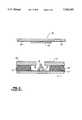
- FIG. 3there is illustrated a portion of a flat panel display comprising a triode structure pixel employing a flat cathode as disclosed within U.S. Pat. No. 5,548,185.
- Display 30comprises an anode which may be configured in the same way as described earlier.
- the anodemay comprise a glass substrate 15, with a conductive layer 20 disposed thereover and a phosphor layer 16 disposed over conductive layer 20.
- An electrical potentialmay be applied to conductive layer 20 for producing the required electric field as described below.
- the cathodecomprises substrate 32, which may have a conductive layer (not shown) deposited thereon, such as shown in FIG. 2.
- Flat cathode emitter 31is then deposited and may comprise a low effective work function material such as amorphic diamond.
- Dielectric film 33is then deposited on substrate 32 in order to support gate electrode 34. Electrical potentials may be applied to conductive layer 20, gate electrode 34 and the conducting layer on substrate 32 (not shown). The operation of display 30 is as described within U.S. Pat. No. 5,548,185.
- Display 40is somewhat based upon the structure and operation of display 30.
- the anodeis as described above with respect to FIG. 3.
- the cathodecomprises substrate 42 which may consist of glass, whereon a thin layer 41 of a non-homogenous LWF material such as cermet, CVD diamond films, aluminum nitrite, gallium nitrite, or amorphic diamond has been deposited thereon.
- a non-homogenous LWF materialsuch as cermet, CVD diamond films, aluminum nitrite, gallium nitrite, or amorphic diamond has been deposited thereon.
- Cermetis an acronym for ceramic and metal, which may be a mixture of an insulating material and a highly conducting material.
- Amorphic diamondis as described in U.S. Pat. Nos. 5,548,185 and 5,449,970.
- layer 41comprises two primary portions 45 and 46. There may be one each of portions 45 and 46 within layer 41 or a plurality of each.
- Portion 45comprises a metal or conductive material (e.g., aluminum, chromium, titanium, molybdenum, graphite), while portion 46 may comprise an insulating material (e.g., diamond, amorphic diamond, aluminum nitrite, gallium nitrite, silicon dioxide).
- insulating materiale.g., diamond, amorphic diamond, aluminum nitrite, gallium nitrite, silicon dioxide.
- What is essentialis the interface 47 between materials 45 and 46. It is conducting-insulating interface 47 where electrons are released upon an application of an electric field (a few volts to 50 volts) between conducting strips 43 and 44. These electrons are then attracted to phosphor layer 16 by an electric field (100-30,000 volts) between the anode and cathode, which is assisted by the application of a potential to conducting layer 20 in the anode
- FIG. 4illustrates that pixel 40 is operable with only one conducting-insulating interface within cathode 41.
- Cathode 41may be fabricated using the following described process. Note, the structures illustrated in FIGS. 5 and 6 may also be constructed using the following fabrication process.
- Substrate 42which may be glass or ceramic, is coated with a thin layer, typically 0.001-1 micron thick, of LWF material using any one of several appropriate deposition techniques.
- a standard photolithographic processinvolving coating of a photoresist, exposure through a mask, development of the photoresist, and etching of the LWF material in order to define the LWF layer into pixel or sub-pixel sized strips or patches of cathode 41. (In FIG. 6, such a pixel patch is shown as item 51.)
- a metal contact depositionfollowed by a standard photolithography to define the electrical contact areas 43 and 44.
- An alternative fabrication methodcould include fabrication of metal contact areas 43 and 44 over substrate 42 prior to depositing LWF patches 41.
- LWF patches 41may be fabricated by use of shadow mask techniques instead of photolithography.
- pixel 50comprises an anode similar to the one described with respect to FIG. 4 and a cathode, which may be comprised with layer 51 of cermet or amorphic diamond.
- the cermet or amorphic diamondmay have many interfaces 47 between conducting material 45 and insulating material 46. These conducting-insulating interfaces 47 have electrons hop up from the interface 47 due to a low voltage applied across metal contacts 43 and 44. These electrons are then caused to bombard phosphor layer 16 by the application of a voltage between the anode and cathode as described above.
- Electrodes 43 and 44may be comprised of aluminum, chromium, titanium, molybdenum, or graphite.
- Electrode layer 20may be comprised of indium tin oxide (ITO).
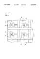
- FIG. 6there is illustrated a portion of a matrix addressable flat panel display.
- the portion illustratedis a top view of four pixels (e.g., pixel 40 or 50) addressable in a manner well-known in the art.
- a cathode layer 51may be addressed by the application of a voltage potential across electrodes 43 and 44 in a matrix-addressable manner.
- cathode layer 51may be replaced by cathode layer 41, shown in FIG. 4.
- the matrix addressing of pixelsmay be performed as discussed within U.S. Pat. No. 5,449,970 or U.S. Pat. No. 5,015,912 which is hereby incorporated by reference herein.
- FIG. 7illustrates a typical hardware configuration of a workstation in accordance with the subject invention having central processing unit 710, such as a conventional microprocessor, and a number of other units interconnected via system bus 712.
- central processing unit 710such as a conventional microprocessor
- system bus 712interconnects system bus 712.
- RAM 714random access memory (RAM) 714, read only memory (ROM) 716, and input/output (I/O) adapter 718 for connecting peripheral devices such as disk units 720 and tape drives 740 to bus 712
- I/Oinput/output
- user interface adapter 722for connecting keyboard 724, mouse 726, speaker 728, microphone 732, and/or other user interface devices such as a touch screen device (not shown) to bus 712
- communication adapter 734for connecting the workstation to a data processing network
- display adapter 736for connecting bus 712 to display device 738.
- Display device 738may be configured as an FED display in accordance with the teachings of the present invention.
Landscapes
- Engineering & Computer Science (AREA)
- Manufacturing & Machinery (AREA)
- Cathode-Ray Tubes And Fluorescent Screens For Display (AREA)
Abstract
Description
Claims (6)
Priority Applications (4)
| Application Number | Priority Date | Filing Date | Title |
|---|---|---|---|
| US08/456,453US5763997A (en) | 1992-03-16 | 1995-06-01 | Field emission display device |
| PCT/US1996/007991WO1996038853A1 (en) | 1995-06-01 | 1996-05-30 | A field emission display device |
| US08/868,644US6127773A (en) | 1992-03-16 | 1997-06-04 | Amorphic diamond film flat field emission cathode |
| US09/677,361US6573643B1 (en) | 1992-03-16 | 2000-10-02 | Field emission light source |
Applications Claiming Priority (3)
| Application Number | Priority Date | Filing Date | Title |
|---|---|---|---|
| US85170192A | 1992-03-16 | 1992-03-16 | |
| US99386392A | 1992-12-23 | 1992-12-23 | |
| US08/456,453US5763997A (en) | 1992-03-16 | 1995-06-01 | Field emission display device |
Related Parent Applications (2)
| Application Number | Title | Priority Date | Filing Date |
|---|---|---|---|
| US99386392AContinuation-In-Part | 1992-03-16 | 1992-12-23 | |
| US99386398AContinuation-In-Part | 1992-03-16 | 1998-12-23 |
Related Child Applications (2)
| Application Number | Title | Priority Date | Filing Date |
|---|---|---|---|
| US85170192AContinuation-In-Part | 1992-03-16 | 1992-03-16 | |
| US08/868,644Continuation-In-PartUS6127773A (en) | 1992-03-16 | 1997-06-04 | Amorphic diamond film flat field emission cathode |
Publications (1)
| Publication Number | Publication Date |
|---|---|
| US5763997Atrue US5763997A (en) | 1998-06-09 |
Family
ID=23812822
Family Applications (1)
| Application Number | Title | Priority Date | Filing Date |
|---|---|---|---|
| US08/456,453Expired - LifetimeUS5763997A (en) | 1992-03-16 | 1995-06-01 | Field emission display device |
Country Status (2)
| Country | Link |
|---|---|
| US (1) | US5763997A (en) |
| WO (1) | WO1996038853A1 (en) |
Cited By (21)
| Publication number | Priority date | Publication date | Assignee | Title |
|---|---|---|---|---|
| US6013980A (en)* | 1997-05-09 | 2000-01-11 | Advanced Refractory Technologies, Inc. | Electrically tunable low secondary electron emission diamond-like coatings and process for depositing coatings |
| US6064148A (en)* | 1997-05-21 | 2000-05-16 | Si Diamond Technology, Inc. | Field emission device |
| WO2001067481A1 (en)* | 2000-03-09 | 2001-09-13 | Si Diamond Technology, Inc. | Triode assembly for carbon cold cathode |
| GB2362753A (en)* | 2000-03-22 | 2001-11-28 | Smiths Group Plc | Display with linear cathode |
| US6351254B2 (en)* | 1998-07-06 | 2002-02-26 | The Regents Of The University Of California | Junction-based field emission structure for field emission display |
| US6417627B1 (en) | 1999-02-03 | 2002-07-09 | Micron Technology, Inc. | Matrix-addressable display with minimum column-row overlap and maximum metal line-width |
| US20030089900A1 (en)* | 2001-04-30 | 2003-05-15 | Zhizhang Chen | Tunneling emitter with nanohole openings |
| US6587097B1 (en) | 2000-11-28 | 2003-07-01 | 3M Innovative Properties Co. | Display system |
| US6586872B2 (en)* | 1997-09-03 | 2003-07-01 | Canon Kabushiki Kaisha | Electron emission source, method and image-forming apparatus, with enhanced output and durability |
| US6590320B1 (en) | 2000-02-23 | 2003-07-08 | Copytale, Inc. | Thin-film planar edge-emitter field emission flat panel display |
| US6642639B2 (en)* | 2000-04-26 | 2003-11-04 | Samsung Sdi Co., Ltd. | Field emission array with carbon nanotubes |
| US6717351B2 (en)* | 1998-12-04 | 2004-04-06 | Micron Technology, Inc. | Apparatus and method for forming cold-cathode field emission displays |
| US20050020176A1 (en)* | 1999-02-17 | 2005-01-27 | Ammar Derraa | Field emission device fabrication methods, field emission base plates, and field emission display devices |
| US6879096B1 (en) | 1999-03-05 | 2005-04-12 | Canon Kabushiki Kaisha | Image formation apparatus |
| US20060055311A1 (en)* | 2004-03-31 | 2006-03-16 | Kyu-Won Jung | Electron emission device and fabrication method and electron emission display |
| USRE39633E1 (en) | 1987-07-15 | 2007-05-15 | Canon Kabushiki Kaisha | Display device with electron-emitting device with electron-emitting region insulated from electrodes |
| CN1316533C (en)* | 2002-02-19 | 2007-05-16 | 法国原子能委员会 | Triode type cathode structure and field emission flat screen |
| USRE40062E1 (en) | 1987-07-15 | 2008-02-12 | Canon Kabushiki Kaisha | Display device with electron-emitting device with electron-emitting region insulated from electrodes |
| US20080160872A1 (en)* | 2003-07-28 | 2008-07-03 | Kabushiki Kaisha Toshiba | Discharge electrode, a discharge lamp and a method for manufacturing the discharge electrode |
| USRE40566E1 (en) | 1987-07-15 | 2008-11-11 | Canon Kabushiki Kaisha | Flat panel display including electron emitting device |
| US20090021136A1 (en)* | 2005-05-31 | 2009-01-22 | Coll Bernard F | Emitting device having electron emitting nanostructures and method of operation |
Families Citing this family (2)
| Publication number | Priority date | Publication date | Assignee | Title |
|---|---|---|---|---|
| KR20070010660A (en)* | 2005-07-19 | 2007-01-24 | 삼성에스디아이 주식회사 | Electron emitting device and flat panel display device having the same |
| JP2007087934A (en)* | 2005-08-24 | 2007-04-05 | Canon Inc | Electron source and image display device |
Citations (194)
| Publication number | Priority date | Publication date | Assignee | Title |
|---|---|---|---|---|
| US1954691A (en)* | 1930-09-27 | 1934-04-10 | Philips Nv | Process of making alpha layer containing alpha fluorescent material |
| US2851408A (en)* | 1954-10-01 | 1958-09-09 | Westinghouse Electric Corp | Method of electrophoretic deposition of luminescent materials and product resulting therefrom |
| US2867541A (en)* | 1957-02-25 | 1959-01-06 | Gen Electric | Method of preparing transparent luminescent screens |
| US2959483A (en)* | 1955-09-06 | 1960-11-08 | Zenith Radio Corp | Color image reproducer and method of manufacture |
| US3070441A (en)* | 1958-02-27 | 1962-12-25 | Rca Corp | Art of manufacturing cathode-ray tubes of the focus-mask variety |
| US3108904A (en)* | 1960-08-30 | 1963-10-29 | Gen Electric | Method of preparing luminescent materials and luminescent screens prepared thereby |
| US3259782A (en)* | 1961-11-08 | 1966-07-05 | Csf | Electron-emissive structure |
| US3314871A (en)* | 1962-12-20 | 1967-04-18 | Columbia Broadcasting Syst Inc | Method of cataphoretic deposition of luminescent materials |
| US3360450A (en)* | 1962-11-19 | 1967-12-26 | American Optical Corp | Method of making cathode ray tube face plates utilizing electrophoretic deposition |
| US3481733A (en)* | 1966-04-18 | 1969-12-02 | Sylvania Electric Prod | Method of forming a cathodo-luminescent screen |
| US3525679A (en)* | 1964-05-05 | 1970-08-25 | Westinghouse Electric Corp | Method of electrodepositing luminescent material on insulating substrate |
| US3554889A (en)* | 1968-11-22 | 1971-01-12 | Ibm | Color cathode ray tube screens |
| US3665241A (en)* | 1970-07-13 | 1972-05-23 | Stanford Research Inst | Field ionizer and field emission cathode structures and methods of production |
| US3675063A (en)* | 1970-01-02 | 1972-07-04 | Stanford Research Inst | High current continuous dynode electron multiplier |
| US3755704A (en)* | 1970-02-06 | 1973-08-28 | Stanford Research Inst | Field emission cathode structures and devices utilizing such structures |
| US3789471A (en)* | 1970-02-06 | 1974-02-05 | Stanford Research Inst | Field emission cathode structures, devices utilizing such structures, and methods of producing such structures |
| US3808048A (en)* | 1970-12-12 | 1974-04-30 | Philips Corp | Method of cataphoretically providing a uniform layer, and colour picture tube comprising such a layer |
| US3812559A (en)* | 1970-07-13 | 1974-05-28 | Stanford Research Inst | Methods of producing field ionizer and field emission cathode structures |
| US3855499A (en)* | 1972-02-25 | 1974-12-17 | Hitachi Ltd | Color display device |
| US3898146A (en)* | 1973-05-07 | 1975-08-05 | Gte Sylvania Inc | Process for fabricating a cathode ray tube screen structure |
| US3947716A (en)* | 1973-08-27 | 1976-03-30 | The United States Of America As Represented By The Secretary Of The Army | Field emission tip and process for making same |
| US3970887A (en)* | 1974-06-19 | 1976-07-20 | Micro-Bit Corporation | Micro-structure field emission electron source |
| US4008412A (en)* | 1974-08-16 | 1977-02-15 | Hitachi, Ltd. | Thin-film field-emission electron source and a method for manufacturing the same |
| US4075535A (en)* | 1975-04-15 | 1978-02-21 | Battelle Memorial Institute | Flat cathodic tube display |
| US4084942A (en)* | 1975-08-27 | 1978-04-18 | Villalobos Humberto Fernandez | Ultrasharp diamond edges and points and method of making |
| US4139773A (en)* | 1977-11-04 | 1979-02-13 | Oregon Graduate Center | Method and apparatus for producing bright high resolution ion beams |
| US4141405A (en)* | 1977-07-27 | 1979-02-27 | Sri International | Method of fabricating a funnel-shaped miniature electrode for use as a field ionization source |
| US4143292A (en)* | 1975-06-27 | 1979-03-06 | Hitachi, Ltd. | Field emission cathode of glassy carbon and method of preparation |
| US4164680A (en)* | 1975-08-27 | 1979-08-14 | Villalobos Humberto F | Polycrystalline diamond emitter |
| US4168213A (en)* | 1976-04-29 | 1979-09-18 | U.S. Philips Corporation | Field emission device and method of forming same |
| US4178531A (en)* | 1977-06-15 | 1979-12-11 | Rca Corporation | CRT with field-emission cathode |
| US4307507A (en)* | 1980-09-10 | 1981-12-29 | The United States Of America As Represented By The Secretary Of The Navy | Method of manufacturing a field-emission cathode structure |
| US4350926A (en)* | 1980-07-28 | 1982-09-21 | The United States Of America As Represented By The Secretary Of The Army | Hollow beam electron source |
| US4482447A (en)* | 1982-09-14 | 1984-11-13 | Sony Corporation | Nonaqueous suspension for electrophoretic deposition of powders |
| US4498952A (en)* | 1982-09-17 | 1985-02-12 | Condesin, Inc. | Batch fabrication procedure for manufacture of arrays of field emitted electron beams with integral self-aligned optical lense in microguns |
| US4507562A (en)* | 1980-10-17 | 1985-03-26 | Jean Gasiot | Methods for rapidly stimulating luminescent phosphors and recovering information therefrom |
| US4513308A (en)* | 1982-09-23 | 1985-04-23 | The United States Of America As Represented By The Secretary Of The Navy | p-n Junction controlled field emitter array cathode |
| US4512912A (en)* | 1983-08-11 | 1985-04-23 | Kabushiki Kaisha Toshiba | White luminescent phosphor for use in cathode ray tube |
| US4528474A (en)* | 1982-03-05 | 1985-07-09 | Kim Jason J | Method and apparatus for producing an electron beam from a thermionic cathode |
| US4540983A (en)* | 1981-10-02 | 1985-09-10 | Futaba Denshi Kogyo K.K. | Fluorescent display device |
| US4542038A (en)* | 1983-09-30 | 1985-09-17 | Hitachi, Ltd. | Method of manufacturing cathode-ray tube |
| US4578614A (en)* | 1982-07-23 | 1986-03-25 | The United States Of America As Represented By The Secretary Of The Navy | Ultra-fast field emitter array vacuum integrated circuit switching device |
| US4588921A (en)* | 1981-01-31 | 1986-05-13 | International Standard Electric Corporation | Vacuum-fluorescent display matrix and method of operating same |
| US4594527A (en)* | 1983-10-06 | 1986-06-10 | Xerox Corporation | Vacuum fluorescent lamp having a flat geometry |
| US4633131A (en)* | 1984-12-12 | 1986-12-30 | North American Philips Corporation | Halo-reducing faceplate arrangement |
| US4647400A (en)* | 1983-06-23 | 1987-03-03 | Centre National De La Recherche Scientifique | Luminescent material or phosphor having a solid matrix within which is distributed a fluorescent compound, its preparation process and its use in a photovoltaic cell |
| US4663559A (en)* | 1982-09-17 | 1987-05-05 | Christensen Alton O | Field emission device |
| US4684540A (en)* | 1986-01-31 | 1987-08-04 | Gte Products Corporation | Coated pigmented phosphors and process for producing same |
| US4684353A (en)* | 1985-08-19 | 1987-08-04 | Dunmore Corporation | Flexible electroluminescent film laminate |
| US4685996A (en)* | 1986-10-14 | 1987-08-11 | Busta Heinz H | Method of making micromachined refractory metal field emitters |
| US4687938A (en)* | 1984-12-17 | 1987-08-18 | Hitachi, Ltd. | Ion source |
| US4687825A (en)* | 1984-03-30 | 1987-08-18 | Kabushiki Kaisha Toshiba | Method of manufacturing phosphor screen of cathode ray tube |
| US4710765A (en)* | 1983-07-30 | 1987-12-01 | Sony Corporation | Luminescent display device |
| US4721885A (en)* | 1987-02-11 | 1988-01-26 | Sri International | Very high speed integrated microelectronic tubes |
| US4728851A (en)* | 1982-01-08 | 1988-03-01 | Ford Motor Company | Field emitter device with gated memory |
| US4758449A (en)* | 1984-06-27 | 1988-07-19 | Matsushita Electronics Corporation | Method for making a phosphor layer |
| US4763187A (en)* | 1984-03-09 | 1988-08-09 | Laboratoire D'etude Des Surfaces | Method of forming images on a flat video screen |
| US4788472A (en)* | 1984-12-13 | 1988-11-29 | Nec Corporation | Fluoroescent display panel having indirectly-heated cathode |
| US4816717A (en)* | 1984-02-06 | 1989-03-28 | Rogers Corporation | Electroluminescent lamp having a polymer phosphor layer formed in substantially a non-crossed linked state |
| US4818914A (en)* | 1987-07-17 | 1989-04-04 | Sri International | High efficiency lamp |
| US4822466A (en)* | 1987-06-25 | 1989-04-18 | University Of Houston - University Park | Chemically bonded diamond films and method for producing same |
| US4827177A (en)* | 1986-09-08 | 1989-05-02 | The General Electric Company, P.L.C. | Field emission vacuum devices |
| US4835438A (en)* | 1986-11-27 | 1989-05-30 | Commissariat A L'energie Atomique | Source of spin polarized electrons using an emissive micropoint cathode |
| US4851254A (en)* | 1987-01-13 | 1989-07-25 | Nippon Soken, Inc. | Method and device for forming diamond film |
| US4855636A (en)* | 1987-10-08 | 1989-08-08 | Busta Heinz H | Micromachined cold cathode vacuum tube device and method of making |
| US4857161A (en)* | 1986-01-24 | 1989-08-15 | Commissariat A L'energie Atomique | Process for the production of a display means by cathodoluminescence excited by field emission |
| US4857799A (en)* | 1986-07-30 | 1989-08-15 | Sri International | Matrix-addressed flat panel display |
| US4874981A (en)* | 1988-05-10 | 1989-10-17 | Sri International | Automatically focusing field emission electrode |
| US4882659A (en)* | 1988-12-21 | 1989-11-21 | Delco Electronics Corporation | Vacuum fluorescent display having integral backlit graphic patterns |
| US4889690A (en)* | 1983-05-28 | 1989-12-26 | Max Planck Gesellschaft | Sensor for measuring physical parameters of concentration of particles |
| US4892757A (en)* | 1988-12-22 | 1990-01-09 | Gte Products Corporation | Method for a producing manganese activated zinc silicate phosphor |
| US4899081A (en)* | 1987-10-02 | 1990-02-06 | Futaba Denshi Kogyo K.K. | Fluorescent display device |
| US4908539A (en)* | 1984-07-24 | 1990-03-13 | Commissariat A L'energie Atomique | Display unit by cathodoluminescence excited by field emission |
| US4923421A (en)* | 1988-07-06 | 1990-05-08 | Innovative Display Development Partners | Method for providing polyimide spacers in a field emission panel display |
| US4926056A (en)* | 1988-06-10 | 1990-05-15 | Sri International | Microelectronic field ionizer and method of fabricating the same |
| US4933108A (en)* | 1978-04-13 | 1990-06-12 | Soeredal Sven G | Emitter for field emission and method of making same |
| US4940916A (en)* | 1987-11-06 | 1990-07-10 | Commissariat A L'energie Atomique | Electron source with micropoint emissive cathodes and display means by cathodoluminescence excited by field emission using said source |
| US4954744A (en)* | 1988-05-26 | 1990-09-04 | Canon Kabushiki Kaisha | Electron-emitting device and electron-beam generator making use |
| US4956202A (en)* | 1988-12-22 | 1990-09-11 | Gte Products Corporation | Firing and milling method for producing a manganese activated zinc silicate phosphor |
| US4956573A (en)* | 1988-12-19 | 1990-09-11 | Babcock Display Products, Inc. | Gas discharge display device with integral, co-planar, built-in heater |
| US4964946A (en)* | 1990-02-02 | 1990-10-23 | The United States Of America As Represented By The Secretary Of The Navy | Process for fabricating self-aligned field emitter arrays |
| US4987007A (en)* | 1988-04-18 | 1991-01-22 | Board Of Regents, The University Of Texas System | Method and apparatus for producing a layer of material from a laser ion source |
| US4990766A (en)* | 1989-05-22 | 1991-02-05 | Murasa International | Solid state electron amplifier |
| US4990416A (en)* | 1989-06-19 | 1991-02-05 | Coloray Display Corporation | Deposition of cathodoluminescent materials by reversal toning |
| US4994205A (en)* | 1989-02-03 | 1991-02-19 | Eastman Kodak Company | Composition containing a hafnia phosphor of enhanced luminescence |
| US5007873A (en)* | 1990-02-09 | 1991-04-16 | Motorola, Inc. | Non-planar field emission device having an emitter formed with a substantially normal vapor deposition process |
| US5015912A (en)* | 1986-07-30 | 1991-05-14 | Sri International | Matrix-addressed flat panel display |
| US5019003A (en)* | 1989-09-29 | 1991-05-28 | Motorola, Inc. | Field emission device having preformed emitters |
| US5036247A (en)* | 1985-09-10 | 1991-07-30 | Pioneer Electronic Corporation | Dot matrix fluorescent display device |
| US5038070A (en)* | 1989-12-26 | 1991-08-06 | Hughes Aircraft Company | Field emitter structure and fabrication process |
| US5054046A (en)* | 1988-01-06 | 1991-10-01 | Jupiter Toy Company | Method of and apparatus for production and manipulation of high density charge |
| US5054047A (en)* | 1988-01-06 | 1991-10-01 | Jupiter Toy Company | Circuits responsive to and controlling charged particles |
| US5055744A (en)* | 1987-12-01 | 1991-10-08 | Futuba Denshi Kogyo K.K. | Display device |
| US5055077A (en)* | 1989-11-22 | 1991-10-08 | Motorola, Inc. | Cold cathode field emission device having an electrode in an encapsulating layer |
| US5057047A (en)* | 1990-09-27 | 1991-10-15 | The United States Of America As Represented By The Secretary Of The Navy | Low capacitance field emitter array and method of manufacture therefor |
| US5063323A (en)* | 1990-07-16 | 1991-11-05 | Hughes Aircraft Company | Field emitter structure providing passageways for venting of outgassed materials from active electronic area |
| US5063327A (en)* | 1988-07-06 | 1991-11-05 | Coloray Display Corporation | Field emission cathode based flat panel display having polyimide spacers |
| US5064396A (en)* | 1990-01-29 | 1991-11-12 | Coloray Display Corporation | Method of manufacturing an electric field producing structure including a field emission cathode |
| US5075595A (en)* | 1991-01-24 | 1991-12-24 | Motorola, Inc. | Field emission device with vertically integrated active control |
| US5075596A (en) | 1990-10-02 | 1991-12-24 | United Technologies Corporation | Electroluminescent display brightness compensation |
| US5075591A (en)* | 1990-07-13 | 1991-12-24 | Coloray Display Corporation | Matrix addressing arrangement for a flat panel display with field emission cathodes |
| US5079476A (en) | 1990-02-09 | 1992-01-07 | Motorola, Inc. | Encapsulated field emission device |
| US5085958A (en) | 1989-08-30 | 1992-02-04 | Samsung Electron Devices Co., Ltd. | Manufacturing method of phosphor film of cathode ray tube |
| US5089812A (en) | 1988-02-26 | 1992-02-18 | Casio Computer Co., Ltd. | Liquid-crystal display |
| US5089742A (en) | 1990-09-28 | 1992-02-18 | The United States Of America As Represented By The Secretary Of The Navy | Electron beam source formed with biologically derived tubule materials |
| US5089292A (en) | 1990-07-20 | 1992-02-18 | Coloray Display Corporation | Field emission cathode array coated with electron work function reducing material, and method |
| US5090932A (en) | 1988-03-25 | 1992-02-25 | Thomson-Csf | Method for the fabrication of field emission type sources, and application thereof to the making of arrays of emitters |
| US5098737A (en) | 1988-04-18 | 1992-03-24 | Board Of Regents The University Of Texas System | Amorphic diamond material produced by laser plasma deposition |
| US5101288A (en) | 1989-04-06 | 1992-03-31 | Ricoh Company, Ltd. | LCD having obliquely split or interdigitated pixels connected to MIM elements having a diamond-like insulator |
| US5103145A (en) | 1990-09-05 | 1992-04-07 | Raytheon Company | Luminance control for cathode-ray tube having field emission cathode |
| US5103144A (en) | 1990-10-01 | 1992-04-07 | Raytheon Company | Brightness control for flat panel display |
| US5117299A (en) | 1989-05-20 | 1992-05-26 | Ricoh Company, Ltd. | Liquid crystal display with a light blocking film of hard carbon |
| US5117267A (en) | 1989-09-27 | 1992-05-26 | Sumitomo Electric Industries, Ltd. | Semiconductor heterojunction structure |
| US5119386A (en) | 1989-01-17 | 1992-06-02 | Matsushita Electric Industrial Co., Ltd. | Light emitting device |
| US5123039A (en) | 1988-01-06 | 1992-06-16 | Jupiter Toy Company | Energy conversion using high charge density |
| US5124558A (en) | 1985-10-10 | 1992-06-23 | Quantex Corporation | Imaging system for mamography employing electron trapping materials |
| US5124072A (en) | 1991-12-02 | 1992-06-23 | General Electric Company | Alkaline earth hafnate phosphor with cerium luminescence |
| US5126287A (en) | 1990-06-07 | 1992-06-30 | Mcnc | Self-aligned electron emitter fabrication method and devices formed thereby |
| US5129850A (en) | 1991-08-20 | 1992-07-14 | Motorola, Inc. | Method of making a molded field emission electron emitter employing a diamond coating |
| US5132676A (en) | 1989-05-24 | 1992-07-21 | Ricoh Company, Ltd. | Liquid crystal display |
| US5132585A (en) | 1990-12-21 | 1992-07-21 | Motorola, Inc. | Projection display faceplate employing an optically transmissive diamond coating of high thermal conductivity |
| US5138237A (en) | 1991-08-20 | 1992-08-11 | Motorola, Inc. | Field emission electron device employing a modulatable diamond semiconductor emitter |
| US5136764A (en) | 1990-09-27 | 1992-08-11 | Motorola, Inc. | Method for forming a field emission device |
| US5140219A (en) | 1991-02-28 | 1992-08-18 | Motorola, Inc. | Field emission display device employing an integral planar field emission control device |
| US5142184A (en) | 1990-02-09 | 1992-08-25 | Kane Robert C | Cold cathode field emission device with integral emitter ballasting |
| US5141460A (en) | 1991-08-20 | 1992-08-25 | Jaskie James E | Method of making a field emission electron source employing a diamond coating |
| US5142256A (en) | 1991-04-04 | 1992-08-25 | Motorola, Inc. | Pin diode with field emission device switch |
| US5141459A (en) | 1990-07-18 | 1992-08-25 | International Business Machines Corporation | Structures and processes for fabricating field emission cathodes |
| US5142390A (en) | 1989-02-23 | 1992-08-25 | Ricoh Company, Ltd. | MIM element with a doped hard carbon film |
| US5144191A (en) | 1991-06-12 | 1992-09-01 | Mcnc | Horizontal microelectronic field emission devices |
| US5148461A (en) | 1988-01-06 | 1992-09-15 | Jupiter Toy Co. | Circuits responsive to and controlling charged particles |
| US5148078A (en) | 1990-08-29 | 1992-09-15 | Motorola, Inc. | Field emission device employing a concentric post |
| US5150011A (en) | 1990-03-30 | 1992-09-22 | Matsushita Electronics Corporation | Gas discharge display device |
| US5150192A (en) | 1990-09-27 | 1992-09-22 | The United States Of America As Represented By The Secretary Of The Navy | Field emitter array |
| US5151061A (en) | 1992-02-21 | 1992-09-29 | Micron Technology, Inc. | Method to form self-aligned tips for flat panel displays |
| US5153753A (en) | 1989-04-12 | 1992-10-06 | Ricoh Company, Ltd. | Active matrix-type liquid crystal display containing a horizontal MIM device with inter-digital conductors |
| US5153901A (en) | 1988-01-06 | 1992-10-06 | Jupiter Toy Company | Production and manipulation of charged particles |
| US5155420A (en) | 1991-08-05 | 1992-10-13 | Smith Robert T | Switching circuits employing field emission devices |
| US5156770A (en) | 1990-06-26 | 1992-10-20 | Thomson Consumer Electronics, Inc. | Conductive contact patch for a CRT faceplate panel |
| US5157309A (en) | 1990-09-13 | 1992-10-20 | Motorola Inc. | Cold-cathode field emission device employing a current source means |
| US5157304A (en) | 1990-12-17 | 1992-10-20 | Motorola, Inc. | Field emission device display with vacuum seal |
| US5162704A (en) | 1991-02-06 | 1992-11-10 | Futaba Denshi Kogyo K.K. | Field emission cathode |
| US5166456A (en) | 1985-12-16 | 1992-11-24 | Kasei Optonix, Ltd. | Luminescent phosphor composition |
| US5173635A (en) | 1990-11-30 | 1992-12-22 | Motorola, Inc. | Bi-directional field emission device |
| US5173697A (en) | 1992-02-05 | 1992-12-22 | Motorola, Inc. | Digital-to-analog signal conversion device employing scaled field emission devices |
| US5173634A (en) | 1990-11-30 | 1992-12-22 | Motorola, Inc. | Current regulated field-emission device |
| US5180951A (en) | 1992-02-05 | 1993-01-19 | Motorola, Inc. | Electron device electron source including a polycrystalline diamond |
| US5183529A (en) | 1990-10-29 | 1993-02-02 | Ford Motor Company | Fabrication of polycrystalline free-standing diamond films |
| US5185178A (en) | 1988-08-29 | 1993-02-09 | Minnesota Mining And Manufacturing Company | Method of forming an array of densely packed discrete metal microspheres |
| US5186670A (en) | 1992-03-02 | 1993-02-16 | Micron Technology, Inc. | Method to form self-aligned gate structures and focus rings |
| US5194780A (en) | 1990-06-13 | 1993-03-16 | Commissariat A L'energie Atomique | Electron source with microtip emissive cathodes |
| US5199918A (en) | 1991-11-07 | 1993-04-06 | Microelectronics And Computer Technology Corporation | Method of forming field emitter device with diamond emission tips |
| US5199917A (en) | 1991-12-09 | 1993-04-06 | Cornell Research Foundation, Inc. | Silicon tip field emission cathode arrays and fabrication thereof |
| US5202571A (en) | 1990-07-06 | 1993-04-13 | Canon Kabushiki Kaisha | Electron emitting device with diamond |
| US5204581A (en) | 1990-07-12 | 1993-04-20 | Bell Communications Research, Inc. | Device including a tapered microminiature silicon structure |
| US5204021A (en) | 1992-01-03 | 1993-04-20 | General Electric Company | Lanthanide oxide fluoride phosphor having cerium luminescence |
| US5203731A (en) | 1990-07-18 | 1993-04-20 | International Business Machines Corporation | Process and structure of an integrated vacuum microelectronic device |
| US5210430A (en) | 1988-12-27 | 1993-05-11 | Canon Kabushiki Kaisha | Electric field light-emitting device |
| US5212426A (en) | 1991-01-24 | 1993-05-18 | Motorola, Inc. | Integrally controlled field emission flat display device |
| US5213712A (en) | 1992-02-10 | 1993-05-25 | General Electric Company | Lanthanum lutetium oxide phosphor with cerium luminescence |
| US5214416A (en) | 1989-12-01 | 1993-05-25 | Ricoh Company, Ltd. | Active matrix board |
| US5214347A (en) | 1990-06-08 | 1993-05-25 | The United States Of America As Represented By The Secretary Of The Navy | Layered thin-edged field-emitter device |
| US5220725A (en) | 1991-04-09 | 1993-06-22 | Northeastern University | Micro-emitter-based low-contact-force interconnection device |
| US5227699A (en) | 1991-08-16 | 1993-07-13 | Amoco Corporation | Recessed gate field emission |
| US5228878A (en) | 1989-12-18 | 1993-07-20 | Seiko Epson Corporation | Field electron emission device production method |
| US5229331A (en) | 1992-02-14 | 1993-07-20 | Micron Technology, Inc. | Method to form self-aligned gate structures around cold cathode emitter tips using chemical mechanical polishing technology |
| US5229682A (en) | 1989-12-18 | 1993-07-20 | Seiko Epson Corporation | Field electron emission device |
| US5228877A (en) | 1991-01-25 | 1993-07-20 | Gec-Marconi Limited | Field emission devices |
| US5231606A (en) | 1990-07-02 | 1993-07-27 | The United States Of America As Represented By The Secretary Of The Navy | Field emitter array memory device |
| US5235244A (en) | 1990-01-29 | 1993-08-10 | Innovative Display Development Partners | Automatically collimating electron beam producing arrangement |
| US5242620A (en) | 1992-07-02 | 1993-09-07 | General Electric Company | Gadolinium lutetium aluminate phosphor with cerium luminescence |
| US5243252A (en) | 1989-12-19 | 1993-09-07 | Matsushita Electric Industrial Co., Ltd. | Electron field emission device |
| US5250451A (en) | 1991-04-23 | 1993-10-05 | France Telecom Etablissement Autonome De Droit Public | Process for the production of thin film transistors |
| US5252833A (en) | 1992-02-05 | 1993-10-12 | Motorola, Inc. | Electron source for depletion mode electron emission apparatus |
| US5256888A (en) | 1992-05-04 | 1993-10-26 | Motorola, Inc. | Transistor device apparatus employing free-space electron emission from a diamond material surface |
| US5259799A (en) | 1992-03-02 | 1993-11-09 | Micron Technology, Inc. | Method to form self-aligned gate structures and focus rings |
| US5266155A (en) | 1990-06-08 | 1993-11-30 | The United States Of America As Represented By The Secretary Of The Navy | Method for making a symmetrical layered thin film edge field-emitter-array |
| US5276521A (en) | 1990-07-30 | 1994-01-04 | Olympus Optical Co., Ltd. | Solid state imaging device having a constant pixel integrating period and blooming resistance |
| US5278475A (en) | 1992-06-01 | 1994-01-11 | Motorola, Inc. | Cathodoluminescent display apparatus and method for realization using diamond crystallites |
| US5277638A (en) | 1992-04-29 | 1994-01-11 | Samsung Electron Devices Co., Ltd. | Method for manufacturing field emission display |
| US5281891A (en) | 1991-02-22 | 1994-01-25 | Matsushita Electric Industrial Co., Ltd. | Electron emission element |
| US5283500A (en) | 1992-05-28 | 1994-02-01 | At&T Bell Laboratories | Flat panel field emission display apparatus |
| US5285129A (en) | 1988-05-31 | 1994-02-08 | Canon Kabushiki Kaisha | Segmented electron emission device |
| US5296117A (en) | 1991-12-11 | 1994-03-22 | Agfa-Gevaert, N.V. | Method for the production of a radiographic screen |
| US5302423A (en) | 1993-07-09 | 1994-04-12 | Minnesota Mining And Manufacturing Company | Method for fabricating pixelized phosphors |
| US5312514A (en) | 1991-11-07 | 1994-05-17 | Microelectronics And Computer Technology Corporation | Method of making a field emitter device using randomly located nuclei as an etch mask |
| US5315393A (en) | 1992-04-01 | 1994-05-24 | Amoco Corporation | Robust pixel array scanning with image signal isolation |
| US5380546A (en) | 1993-06-09 | 1995-01-10 | Microelectronics And Computer Technology Corporation | Multilevel metallization process for electronic components |
| US5399238A (en) | 1991-11-07 | 1995-03-21 | Microelectronics And Computer Technology Corporation | Method of making field emission tips using physical vapor deposition of random nuclei as etch mask |
| US5449970A (en) | 1992-03-16 | 1995-09-12 | Microelectronics And Computer Technology Corporation | Diode structure flat panel display |
| US5531880A (en) | 1994-09-13 | 1996-07-02 | Microelectronics And Computer Technology Corporation | Method for producing thin, uniform powder phosphor for display screens |
| US5536193A (en) | 1991-11-07 | 1996-07-16 | Microelectronics And Computer Technology Corporation | Method of making wide band gap field emitter |
| US5543684A (en) | 1992-03-16 | 1996-08-06 | Microelectronics And Computer Technology Corporation | Flat panel display based on diamond thin films |
| US5548185A (en) | 1992-03-16 | 1996-08-20 | Microelectronics And Computer Technology Corporation | Triode structure flat panel display employing flat field emission cathode |
- 1995
- 1995-06-01USUS08/456,453patent/US5763997A/ennot_activeExpired - Lifetime
- 1996
- 1996-05-30WOPCT/US1996/007991patent/WO1996038853A1/enactiveApplication Filing
Patent Citations (200)
| Publication number | Priority date | Publication date | Assignee | Title |
|---|---|---|---|---|
| US1954691A (en)* | 1930-09-27 | 1934-04-10 | Philips Nv | Process of making alpha layer containing alpha fluorescent material |
| US2851408A (en)* | 1954-10-01 | 1958-09-09 | Westinghouse Electric Corp | Method of electrophoretic deposition of luminescent materials and product resulting therefrom |
| US2959483A (en)* | 1955-09-06 | 1960-11-08 | Zenith Radio Corp | Color image reproducer and method of manufacture |
| US2867541A (en)* | 1957-02-25 | 1959-01-06 | Gen Electric | Method of preparing transparent luminescent screens |
| US3070441A (en)* | 1958-02-27 | 1962-12-25 | Rca Corp | Art of manufacturing cathode-ray tubes of the focus-mask variety |
| US3108904A (en)* | 1960-08-30 | 1963-10-29 | Gen Electric | Method of preparing luminescent materials and luminescent screens prepared thereby |
| US3259782A (en)* | 1961-11-08 | 1966-07-05 | Csf | Electron-emissive structure |
| US3360450A (en)* | 1962-11-19 | 1967-12-26 | American Optical Corp | Method of making cathode ray tube face plates utilizing electrophoretic deposition |
| US3314871A (en)* | 1962-12-20 | 1967-04-18 | Columbia Broadcasting Syst Inc | Method of cataphoretic deposition of luminescent materials |
| US3525679A (en)* | 1964-05-05 | 1970-08-25 | Westinghouse Electric Corp | Method of electrodepositing luminescent material on insulating substrate |
| US3481733A (en)* | 1966-04-18 | 1969-12-02 | Sylvania Electric Prod | Method of forming a cathodo-luminescent screen |
| US3554889A (en)* | 1968-11-22 | 1971-01-12 | Ibm | Color cathode ray tube screens |
| US3675063A (en)* | 1970-01-02 | 1972-07-04 | Stanford Research Inst | High current continuous dynode electron multiplier |
| US3755704A (en)* | 1970-02-06 | 1973-08-28 | Stanford Research Inst | Field emission cathode structures and devices utilizing such structures |
| US3789471A (en)* | 1970-02-06 | 1974-02-05 | Stanford Research Inst | Field emission cathode structures, devices utilizing such structures, and methods of producing such structures |
| US3812559A (en)* | 1970-07-13 | 1974-05-28 | Stanford Research Inst | Methods of producing field ionizer and field emission cathode structures |
| US3665241A (en)* | 1970-07-13 | 1972-05-23 | Stanford Research Inst | Field ionizer and field emission cathode structures and methods of production |
| US3808048A (en)* | 1970-12-12 | 1974-04-30 | Philips Corp | Method of cataphoretically providing a uniform layer, and colour picture tube comprising such a layer |
| US3855499A (en)* | 1972-02-25 | 1974-12-17 | Hitachi Ltd | Color display device |
| US3898146A (en)* | 1973-05-07 | 1975-08-05 | Gte Sylvania Inc | Process for fabricating a cathode ray tube screen structure |
| US3947716A (en)* | 1973-08-27 | 1976-03-30 | The United States Of America As Represented By The Secretary Of The Army | Field emission tip and process for making same |
| US3970887A (en)* | 1974-06-19 | 1976-07-20 | Micro-Bit Corporation | Micro-structure field emission electron source |
| US4008412A (en)* | 1974-08-16 | 1977-02-15 | Hitachi, Ltd. | Thin-film field-emission electron source and a method for manufacturing the same |
| US4075535A (en)* | 1975-04-15 | 1978-02-21 | Battelle Memorial Institute | Flat cathodic tube display |
| US4143292A (en)* | 1975-06-27 | 1979-03-06 | Hitachi, Ltd. | Field emission cathode of glassy carbon and method of preparation |
| US4084942A (en)* | 1975-08-27 | 1978-04-18 | Villalobos Humberto Fernandez | Ultrasharp diamond edges and points and method of making |
| US4164680A (en)* | 1975-08-27 | 1979-08-14 | Villalobos Humberto F | Polycrystalline diamond emitter |
| US4168213A (en)* | 1976-04-29 | 1979-09-18 | U.S. Philips Corporation | Field emission device and method of forming same |
| US4178531A (en)* | 1977-06-15 | 1979-12-11 | Rca Corporation | CRT with field-emission cathode |
| US4141405A (en)* | 1977-07-27 | 1979-02-27 | Sri International | Method of fabricating a funnel-shaped miniature electrode for use as a field ionization source |
| US4139773A (en)* | 1977-11-04 | 1979-02-13 | Oregon Graduate Center | Method and apparatus for producing bright high resolution ion beams |
| US4933108A (en)* | 1978-04-13 | 1990-06-12 | Soeredal Sven G | Emitter for field emission and method of making same |
| US4350926A (en)* | 1980-07-28 | 1982-09-21 | The United States Of America As Represented By The Secretary Of The Army | Hollow beam electron source |
| US4307507A (en)* | 1980-09-10 | 1981-12-29 | The United States Of America As Represented By The Secretary Of The Navy | Method of manufacturing a field-emission cathode structure |
| US4507562A (en)* | 1980-10-17 | 1985-03-26 | Jean Gasiot | Methods for rapidly stimulating luminescent phosphors and recovering information therefrom |
| US4588921A (en)* | 1981-01-31 | 1986-05-13 | International Standard Electric Corporation | Vacuum-fluorescent display matrix and method of operating same |
| US4540983A (en)* | 1981-10-02 | 1985-09-10 | Futaba Denshi Kogyo K.K. | Fluorescent display device |
| US4728851A (en)* | 1982-01-08 | 1988-03-01 | Ford Motor Company | Field emitter device with gated memory |
| US4528474A (en)* | 1982-03-05 | 1985-07-09 | Kim Jason J | Method and apparatus for producing an electron beam from a thermionic cathode |
| US4578614A (en)* | 1982-07-23 | 1986-03-25 | The United States Of America As Represented By The Secretary Of The Navy | Ultra-fast field emitter array vacuum integrated circuit switching device |
| US4482447A (en)* | 1982-09-14 | 1984-11-13 | Sony Corporation | Nonaqueous suspension for electrophoretic deposition of powders |
| US4498952A (en)* | 1982-09-17 | 1985-02-12 | Condesin, Inc. | Batch fabrication procedure for manufacture of arrays of field emitted electron beams with integral self-aligned optical lense in microguns |
| US4663559A (en)* | 1982-09-17 | 1987-05-05 | Christensen Alton O | Field emission device |
| US4513308A (en)* | 1982-09-23 | 1985-04-23 | The United States Of America As Represented By The Secretary Of The Navy | p-n Junction controlled field emitter array cathode |
| US4889690A (en)* | 1983-05-28 | 1989-12-26 | Max Planck Gesellschaft | Sensor for measuring physical parameters of concentration of particles |
| US4647400A (en)* | 1983-06-23 | 1987-03-03 | Centre National De La Recherche Scientifique | Luminescent material or phosphor having a solid matrix within which is distributed a fluorescent compound, its preparation process and its use in a photovoltaic cell |
| US4710765A (en)* | 1983-07-30 | 1987-12-01 | Sony Corporation | Luminescent display device |
| US4512912A (en)* | 1983-08-11 | 1985-04-23 | Kabushiki Kaisha Toshiba | White luminescent phosphor for use in cathode ray tube |
| US4542038A (en)* | 1983-09-30 | 1985-09-17 | Hitachi, Ltd. | Method of manufacturing cathode-ray tube |
| US4594527A (en)* | 1983-10-06 | 1986-06-10 | Xerox Corporation | Vacuum fluorescent lamp having a flat geometry |
| US4816717A (en)* | 1984-02-06 | 1989-03-28 | Rogers Corporation | Electroluminescent lamp having a polymer phosphor layer formed in substantially a non-crossed linked state |
| US4763187B1 (en)* | 1984-03-09 | 1997-11-04 | Etude Des Surfaces Lab | Method of forming images on a flat video screen |
| US4763187A (en)* | 1984-03-09 | 1988-08-09 | Laboratoire D'etude Des Surfaces | Method of forming images on a flat video screen |
| US4687825A (en)* | 1984-03-30 | 1987-08-18 | Kabushiki Kaisha Toshiba | Method of manufacturing phosphor screen of cathode ray tube |
| US4758449A (en)* | 1984-06-27 | 1988-07-19 | Matsushita Electronics Corporation | Method for making a phosphor layer |
| US4908539A (en)* | 1984-07-24 | 1990-03-13 | Commissariat A L'energie Atomique | Display unit by cathodoluminescence excited by field emission |
| US4633131A (en)* | 1984-12-12 | 1986-12-30 | North American Philips Corporation | Halo-reducing faceplate arrangement |
| US4788472A (en)* | 1984-12-13 | 1988-11-29 | Nec Corporation | Fluoroescent display panel having indirectly-heated cathode |
| US4687938A (en)* | 1984-12-17 | 1987-08-18 | Hitachi, Ltd. | Ion source |
| US4684353A (en)* | 1985-08-19 | 1987-08-04 | Dunmore Corporation | Flexible electroluminescent film laminate |
| US5036247A (en)* | 1985-09-10 | 1991-07-30 | Pioneer Electronic Corporation | Dot matrix fluorescent display device |
| US5124558A (en) | 1985-10-10 | 1992-06-23 | Quantex Corporation | Imaging system for mamography employing electron trapping materials |
| US5166456A (en) | 1985-12-16 | 1992-11-24 | Kasei Optonix, Ltd. | Luminescent phosphor composition |
| US4857161A (en)* | 1986-01-24 | 1989-08-15 | Commissariat A L'energie Atomique | Process for the production of a display means by cathodoluminescence excited by field emission |
| US4684540A (en)* | 1986-01-31 | 1987-08-04 | Gte Products Corporation | Coated pigmented phosphors and process for producing same |
| US4857799A (en)* | 1986-07-30 | 1989-08-15 | Sri International | Matrix-addressed flat panel display |
| US5015912A (en)* | 1986-07-30 | 1991-05-14 | Sri International | Matrix-addressed flat panel display |
| US4827177A (en)* | 1986-09-08 | 1989-05-02 | The General Electric Company, P.L.C. | Field emission vacuum devices |
| US4685996A (en)* | 1986-10-14 | 1987-08-11 | Busta Heinz H | Method of making micromachined refractory metal field emitters |
| US4835438A (en)* | 1986-11-27 | 1989-05-30 | Commissariat A L'energie Atomique | Source of spin polarized electrons using an emissive micropoint cathode |
| US4851254A (en)* | 1987-01-13 | 1989-07-25 | Nippon Soken, Inc. | Method and device for forming diamond film |
| US4721885A (en)* | 1987-02-11 | 1988-01-26 | Sri International | Very high speed integrated microelectronic tubes |
| US4822466A (en)* | 1987-06-25 | 1989-04-18 | University Of Houston - University Park | Chemically bonded diamond films and method for producing same |
| US4818914A (en)* | 1987-07-17 | 1989-04-04 | Sri International | High efficiency lamp |
| US4899081A (en)* | 1987-10-02 | 1990-02-06 | Futaba Denshi Kogyo K.K. | Fluorescent display device |
| US4855636A (en)* | 1987-10-08 | 1989-08-08 | Busta Heinz H | Micromachined cold cathode vacuum tube device and method of making |
| US4940916A (en)* | 1987-11-06 | 1990-07-10 | Commissariat A L'energie Atomique | Electron source with micropoint emissive cathodes and display means by cathodoluminescence excited by field emission using said source |
| US4940916B1 (en)* | 1987-11-06 | 1996-11-26 | Commissariat Energie Atomique | Electron source with micropoint emissive cathodes and display means by cathodoluminescence excited by field emission using said source |
| US5055744A (en)* | 1987-12-01 | 1991-10-08 | Futuba Denshi Kogyo K.K. | Display device |
| US5123039A (en) | 1988-01-06 | 1992-06-16 | Jupiter Toy Company | Energy conversion using high charge density |
| US5153901A (en) | 1988-01-06 | 1992-10-06 | Jupiter Toy Company | Production and manipulation of charged particles |
| US5148461A (en) | 1988-01-06 | 1992-09-15 | Jupiter Toy Co. | Circuits responsive to and controlling charged particles |
| US5054047A (en)* | 1988-01-06 | 1991-10-01 | Jupiter Toy Company | Circuits responsive to and controlling charged particles |
| US5054046A (en)* | 1988-01-06 | 1991-10-01 | Jupiter Toy Company | Method of and apparatus for production and manipulation of high density charge |
| US5089812A (en) | 1988-02-26 | 1992-02-18 | Casio Computer Co., Ltd. | Liquid-crystal display |
| US5090932A (en) | 1988-03-25 | 1992-02-25 | Thomson-Csf | Method for the fabrication of field emission type sources, and application thereof to the making of arrays of emitters |
| US4987007A (en)* | 1988-04-18 | 1991-01-22 | Board Of Regents, The University Of Texas System | Method and apparatus for producing a layer of material from a laser ion source |
| US5098737A (en) | 1988-04-18 | 1992-03-24 | Board Of Regents The University Of Texas System | Amorphic diamond material produced by laser plasma deposition |
| US4874981A (en)* | 1988-05-10 | 1989-10-17 | Sri International | Automatically focusing field emission electrode |
| US4954744A (en)* | 1988-05-26 | 1990-09-04 | Canon Kabushiki Kaisha | Electron-emitting device and electron-beam generator making use |
| US5285129A (en) | 1988-05-31 | 1994-02-08 | Canon Kabushiki Kaisha | Segmented electron emission device |
| US4926056A (en)* | 1988-06-10 | 1990-05-15 | Sri International | Microelectronic field ionizer and method of fabricating the same |
| US4923421A (en)* | 1988-07-06 | 1990-05-08 | Innovative Display Development Partners | Method for providing polyimide spacers in a field emission panel display |
| US5063327A (en)* | 1988-07-06 | 1991-11-05 | Coloray Display Corporation | Field emission cathode based flat panel display having polyimide spacers |
| US5185178A (en) | 1988-08-29 | 1993-02-09 | Minnesota Mining And Manufacturing Company | Method of forming an array of densely packed discrete metal microspheres |
| US4956573A (en)* | 1988-12-19 | 1990-09-11 | Babcock Display Products, Inc. | Gas discharge display device with integral, co-planar, built-in heater |
| US4882659A (en)* | 1988-12-21 | 1989-11-21 | Delco Electronics Corporation | Vacuum fluorescent display having integral backlit graphic patterns |
| US4956202A (en)* | 1988-12-22 | 1990-09-11 | Gte Products Corporation | Firing and milling method for producing a manganese activated zinc silicate phosphor |
| US4892757A (en)* | 1988-12-22 | 1990-01-09 | Gte Products Corporation | Method for a producing manganese activated zinc silicate phosphor |
| US5210430A (en) | 1988-12-27 | 1993-05-11 | Canon Kabushiki Kaisha | Electric field light-emitting device |
| US5275967A (en) | 1988-12-27 | 1994-01-04 | Canon Kabushiki Kaisha | Electric field light-emitting device |
| US5119386A (en) | 1989-01-17 | 1992-06-02 | Matsushita Electric Industrial Co., Ltd. | Light emitting device |
| US4994205A (en)* | 1989-02-03 | 1991-02-19 | Eastman Kodak Company | Composition containing a hafnia phosphor of enhanced luminescence |
| US5142390A (en) | 1989-02-23 | 1992-08-25 | Ricoh Company, Ltd. | MIM element with a doped hard carbon film |
| US5101288A (en) | 1989-04-06 | 1992-03-31 | Ricoh Company, Ltd. | LCD having obliquely split or interdigitated pixels connected to MIM elements having a diamond-like insulator |
| US5153753A (en) | 1989-04-12 | 1992-10-06 | Ricoh Company, Ltd. | Active matrix-type liquid crystal display containing a horizontal MIM device with inter-digital conductors |
| US5117299A (en) | 1989-05-20 | 1992-05-26 | Ricoh Company, Ltd. | Liquid crystal display with a light blocking film of hard carbon |
| US4990766A (en)* | 1989-05-22 | 1991-02-05 | Murasa International | Solid state electron amplifier |
| US5132676A (en) | 1989-05-24 | 1992-07-21 | Ricoh Company, Ltd. | Liquid crystal display |
| US4990416A (en)* | 1989-06-19 | 1991-02-05 | Coloray Display Corporation | Deposition of cathodoluminescent materials by reversal toning |
| US5085958A (en) | 1989-08-30 | 1992-02-04 | Samsung Electron Devices Co., Ltd. | Manufacturing method of phosphor film of cathode ray tube |
| US5117267A (en) | 1989-09-27 | 1992-05-26 | Sumitomo Electric Industries, Ltd. | Semiconductor heterojunction structure |
| US5019003A (en)* | 1989-09-29 | 1991-05-28 | Motorola, Inc. | Field emission device having preformed emitters |
| US5055077A (en)* | 1989-11-22 | 1991-10-08 | Motorola, Inc. | Cold cathode field emission device having an electrode in an encapsulating layer |
| US5214416A (en) | 1989-12-01 | 1993-05-25 | Ricoh Company, Ltd. | Active matrix board |
| US5229682A (en) | 1989-12-18 | 1993-07-20 | Seiko Epson Corporation | Field electron emission device |
| US5228878A (en) | 1989-12-18 | 1993-07-20 | Seiko Epson Corporation | Field electron emission device production method |
| US5243252A (en) | 1989-12-19 | 1993-09-07 | Matsushita Electric Industrial Co., Ltd. | Electron field emission device |
| US5038070A (en)* | 1989-12-26 | 1991-08-06 | Hughes Aircraft Company | Field emitter structure and fabrication process |
| US5235244A (en) | 1990-01-29 | 1993-08-10 | Innovative Display Development Partners | Automatically collimating electron beam producing arrangement |
| US5064396A (en)* | 1990-01-29 | 1991-11-12 | Coloray Display Corporation | Method of manufacturing an electric field producing structure including a field emission cathode |
| US4964946A (en)* | 1990-02-02 | 1990-10-23 | The United States Of America As Represented By The Secretary Of The Navy | Process for fabricating self-aligned field emitter arrays |
| US5142184B1 (en) | 1990-02-09 | 1995-11-21 | Motorola Inc | Cold cathode field emission device with integral emitter ballasting |
| US5142184A (en) | 1990-02-09 | 1992-08-25 | Kane Robert C | Cold cathode field emission device with integral emitter ballasting |
| US5007873A (en)* | 1990-02-09 | 1991-04-16 | Motorola, Inc. | Non-planar field emission device having an emitter formed with a substantially normal vapor deposition process |
| US5079476A (en) | 1990-02-09 | 1992-01-07 | Motorola, Inc. | Encapsulated field emission device |
| US5150011A (en) | 1990-03-30 | 1992-09-22 | Matsushita Electronics Corporation | Gas discharge display device |
| US5126287A (en) | 1990-06-07 | 1992-06-30 | Mcnc | Self-aligned electron emitter fabrication method and devices formed thereby |
| US5214347A (en) | 1990-06-08 | 1993-05-25 | The United States Of America As Represented By The Secretary Of The Navy | Layered thin-edged field-emitter device |
| US5266155A (en) | 1990-06-08 | 1993-11-30 | The United States Of America As Represented By The Secretary Of The Navy | Method for making a symmetrical layered thin film edge field-emitter-array |
| US5194780A (en) | 1990-06-13 | 1993-03-16 | Commissariat A L'energie Atomique | Electron source with microtip emissive cathodes |
| US5156770A (en) | 1990-06-26 | 1992-10-20 | Thomson Consumer Electronics, Inc. | Conductive contact patch for a CRT faceplate panel |
| US5231606A (en) | 1990-07-02 | 1993-07-27 | The United States Of America As Represented By The Secretary Of The Navy | Field emitter array memory device |
| US5202571A (en) | 1990-07-06 | 1993-04-13 | Canon Kabushiki Kaisha | Electron emitting device with diamond |
| US5204581A (en) | 1990-07-12 | 1993-04-20 | Bell Communications Research, Inc. | Device including a tapered microminiature silicon structure |
| US5075591A (en)* | 1990-07-13 | 1991-12-24 | Coloray Display Corporation | Matrix addressing arrangement for a flat panel display with field emission cathodes |
| US5063323A (en)* | 1990-07-16 | 1991-11-05 | Hughes Aircraft Company | Field emitter structure providing passageways for venting of outgassed materials from active electronic area |
| US5203731A (en) | 1990-07-18 | 1993-04-20 | International Business Machines Corporation | Process and structure of an integrated vacuum microelectronic device |
| US5141459A (en) | 1990-07-18 | 1992-08-25 | International Business Machines Corporation | Structures and processes for fabricating field emission cathodes |
| US5089292A (en) | 1990-07-20 | 1992-02-18 | Coloray Display Corporation | Field emission cathode array coated with electron work function reducing material, and method |
| US5276521A (en) | 1990-07-30 | 1994-01-04 | Olympus Optical Co., Ltd. | Solid state imaging device having a constant pixel integrating period and blooming resistance |
| US5148078A (en) | 1990-08-29 | 1992-09-15 | Motorola, Inc. | Field emission device employing a concentric post |
| US5103145A (en) | 1990-09-05 | 1992-04-07 | Raytheon Company | Luminance control for cathode-ray tube having field emission cathode |
| US5157309A (en) | 1990-09-13 | 1992-10-20 | Motorola Inc. | Cold-cathode field emission device employing a current source means |
| US5136764A (en) | 1990-09-27 | 1992-08-11 | Motorola, Inc. | Method for forming a field emission device |
| US5150192A (en) | 1990-09-27 | 1992-09-22 | The United States Of America As Represented By The Secretary Of The Navy | Field emitter array |
| US5057047A (en)* | 1990-09-27 | 1991-10-15 | The United States Of America As Represented By The Secretary Of The Navy | Low capacitance field emitter array and method of manufacture therefor |
| US5089742A (en) | 1990-09-28 | 1992-02-18 | The United States Of America As Represented By The Secretary Of The Navy | Electron beam source formed with biologically derived tubule materials |
| US5103144A (en) | 1990-10-01 | 1992-04-07 | Raytheon Company | Brightness control for flat panel display |
| US5075596A (en) | 1990-10-02 | 1991-12-24 | United Technologies Corporation | Electroluminescent display brightness compensation |
| US5183529A (en) | 1990-10-29 | 1993-02-02 | Ford Motor Company | Fabrication of polycrystalline free-standing diamond films |
| US5173635A (en) | 1990-11-30 | 1992-12-22 | Motorola, Inc. | Bi-directional field emission device |
| US5173634A (en) | 1990-11-30 | 1992-12-22 | Motorola, Inc. | Current regulated field-emission device |
| US5157304A (en) | 1990-12-17 | 1992-10-20 | Motorola, Inc. | Field emission device display with vacuum seal |
| US5132585A (en) | 1990-12-21 | 1992-07-21 | Motorola, Inc. | Projection display faceplate employing an optically transmissive diamond coating of high thermal conductivity |
| US5075595A (en)* | 1991-01-24 | 1991-12-24 | Motorola, Inc. | Field emission device with vertically integrated active control |
| US5212426A (en) | 1991-01-24 | 1993-05-18 | Motorola, Inc. | Integrally controlled field emission flat display device |
| US5228877A (en) | 1991-01-25 | 1993-07-20 | Gec-Marconi Limited | Field emission devices |
| US5162704A (en) | 1991-02-06 | 1992-11-10 | Futaba Denshi Kogyo K.K. | Field emission cathode |
| US5281891A (en) | 1991-02-22 | 1994-01-25 | Matsushita Electric Industrial Co., Ltd. | Electron emission element |
| US5140219A (en) | 1991-02-28 | 1992-08-18 | Motorola, Inc. | Field emission display device employing an integral planar field emission control device |
| US5142256A (en) | 1991-04-04 | 1992-08-25 | Motorola, Inc. | Pin diode with field emission device switch |
| US5220725A (en) | 1991-04-09 | 1993-06-22 | Northeastern University | Micro-emitter-based low-contact-force interconnection device |
| US5250451A (en) | 1991-04-23 | 1993-10-05 | France Telecom Etablissement Autonome De Droit Public | Process for the production of thin film transistors |
| US5144191A (en) | 1991-06-12 | 1992-09-01 | Mcnc | Horizontal microelectronic field emission devices |
| US5155420A (en) | 1991-08-05 | 1992-10-13 | Smith Robert T | Switching circuits employing field emission devices |
| US5227699A (en) | 1991-08-16 | 1993-07-13 | Amoco Corporation | Recessed gate field emission |
| US5138237A (en) | 1991-08-20 | 1992-08-11 | Motorola, Inc. | Field emission electron device employing a modulatable diamond semiconductor emitter |
| US5141460A (en) | 1991-08-20 | 1992-08-25 | Jaskie James E | Method of making a field emission electron source employing a diamond coating |
| US5129850A (en) | 1991-08-20 | 1992-07-14 | Motorola, Inc. | Method of making a molded field emission electron emitter employing a diamond coating |
| US5199918A (en) | 1991-11-07 | 1993-04-06 | Microelectronics And Computer Technology Corporation | Method of forming field emitter device with diamond emission tips |
| US5536193A (en) | 1991-11-07 | 1996-07-16 | Microelectronics And Computer Technology Corporation | Method of making wide band gap field emitter |
| US5312514A (en) | 1991-11-07 | 1994-05-17 | Microelectronics And Computer Technology Corporation | Method of making a field emitter device using randomly located nuclei as an etch mask |
| US5341063A (en) | 1991-11-07 | 1994-08-23 | Microelectronics And Computer Technology Corporation | Field emitter with diamond emission tips |
| US5399238A (en) | 1991-11-07 | 1995-03-21 | Microelectronics And Computer Technology Corporation | Method of making field emission tips using physical vapor deposition of random nuclei as etch mask |
| US5124072A (en) | 1991-12-02 | 1992-06-23 | General Electric Company | Alkaline earth hafnate phosphor with cerium luminescence |
| US5199917A (en) | 1991-12-09 | 1993-04-06 | Cornell Research Foundation, Inc. | Silicon tip field emission cathode arrays and fabrication thereof |
| US5296117A (en) | 1991-12-11 | 1994-03-22 | Agfa-Gevaert, N.V. | Method for the production of a radiographic screen |
| US5204021A (en) | 1992-01-03 | 1993-04-20 | General Electric Company | Lanthanide oxide fluoride phosphor having cerium luminescence |
| US5173697A (en) | 1992-02-05 | 1992-12-22 | Motorola, Inc. | Digital-to-analog signal conversion device employing scaled field emission devices |
| US5180951A (en) | 1992-02-05 | 1993-01-19 | Motorola, Inc. | Electron device electron source including a polycrystalline diamond |
| US5252833A (en) | 1992-02-05 | 1993-10-12 | Motorola, Inc. | Electron source for depletion mode electron emission apparatus |
| US5213712A (en) | 1992-02-10 | 1993-05-25 | General Electric Company | Lanthanum lutetium oxide phosphor with cerium luminescence |
| US5229331A (en) | 1992-02-14 | 1993-07-20 | Micron Technology, Inc. | Method to form self-aligned gate structures around cold cathode emitter tips using chemical mechanical polishing technology |
| US5151061A (en) | 1992-02-21 | 1992-09-29 | Micron Technology, Inc. | Method to form self-aligned tips for flat panel displays |
| US5186670A (en) | 1992-03-02 | 1993-02-16 | Micron Technology, Inc. | Method to form self-aligned gate structures and focus rings |
| US5259799A (en) | 1992-03-02 | 1993-11-09 | Micron Technology, Inc. | Method to form self-aligned gate structures and focus rings |
| US5548185A (en) | 1992-03-16 | 1996-08-20 | Microelectronics And Computer Technology Corporation | Triode structure flat panel display employing flat field emission cathode |
| US5449970A (en) | 1992-03-16 | 1995-09-12 | Microelectronics And Computer Technology Corporation | Diode structure flat panel display |
| US5551903A (en) | 1992-03-16 | 1996-09-03 | Microelectronics And Computer Technology | Flat panel display based on diamond thin films |
| US5543684A (en) | 1992-03-16 | 1996-08-06 | Microelectronics And Computer Technology Corporation | Flat panel display based on diamond thin films |
| US5315393A (en) | 1992-04-01 | 1994-05-24 | Amoco Corporation | Robust pixel array scanning with image signal isolation |
| US5277638A (en) | 1992-04-29 | 1994-01-11 | Samsung Electron Devices Co., Ltd. | Method for manufacturing field emission display |
| US5256888A (en) | 1992-05-04 | 1993-10-26 | Motorola, Inc. | Transistor device apparatus employing free-space electron emission from a diamond material surface |
| US5283500A (en) | 1992-05-28 | 1994-02-01 | At&T Bell Laboratories | Flat panel field emission display apparatus |
| US5278475A (en) | 1992-06-01 | 1994-01-11 | Motorola, Inc. | Cathodoluminescent display apparatus and method for realization using diamond crystallites |
| US5242620A (en) | 1992-07-02 | 1993-09-07 | General Electric Company | Gadolinium lutetium aluminate phosphor with cerium luminescence |
| US5380546A (en) | 1993-06-09 | 1995-01-10 | Microelectronics And Computer Technology Corporation | Multilevel metallization process for electronic components |
| US5302423A (en) | 1993-07-09 | 1994-04-12 | Minnesota Mining And Manufacturing Company | Method for fabricating pixelized phosphors |
| US5531880A (en) | 1994-09-13 | 1996-07-02 | Microelectronics And Computer Technology Corporation | Method for producing thin, uniform powder phosphor for display screens |
Non-Patent Citations (92)
| Title |
|---|
| "A Comparative Study of Deposition of Thin Films by Laser Induced PVD with Femtosecond and Nanosecond Laser Pulses," SPIE, vol. 1858 (1993), pp. 464-475. |
| "A New Vacuum-Etched High-Transmittance (Antireflection) Film", Appl. Phys. Lett. pp. 727-730 (1980). |
| "Amorphic Diamond Films Produced by a Laser Plasma Source," Journal Appl. Physics, vol. 67, No. 4, Feb. 15, 1990, pp. 2081-2087. |
| "Angular Characteristics of the Radiation by Ultra Relativistic Electrons in Thick Diamond Single Crystals," Sov. Tech. Phys. Lett. vol. 11, No. 11, Nov. 1985, pp. 574-575. |
| "Cathodoluminescence: Theory and Application," VCH Publishers, New York, 1990, Chapters 9 and 10. |
| "Cathodoluminescent Materials," Electron Tube Design, D. Sarnoff Res. Center Yearly Reports & Review, 1976, pp. 128-137. |
| "Characterization of Laser Vaporization Plasmas Generated for the Deposition of Diamond-Like Carbon," J. Appl. Phys., vol. 72, No. 9, Nov. 1, 1992, pp. 3966-3970. |
| "Cold Field Emission From CVD Diamond Films Observed in Emission Electron Microscopy," 1991. |
| "Cone Formation as a Result of Whisker Growth on Ion Bombarded Metal Surfaces," J. Vac. Sci. Technol. A 3(4), Jul./Aug. 1985, pp. 1821-1834. |
| "Cone Formation on Metal Targets During Sputtering," J. Appl. Physics. vol. 42, No. 3, Mar. 1, 1971, pp. 1145-1149. |
| "Control of Silicon Field Emitter Shaper with Isotrophically Etched Oxide Masks," Dec. 1989. |
| "Deposition of Amorphous Carbon from Laser-Produced Plasmas," Mat. Res. Soc. Sump. Proc. vol. 38, (1985), pp. 326-335. |
| "Development of Nano-Crystaline Diamond-Based Field-Emission Displays,"0 Society of Information Display Conference Technical Digest, 1994, pp. 43-45. |
| "Diamond Cold Cathode," IEEE Electron Device Letters, vol. 12, No. 8, (Aug. 1989) pp. 456-459. |
| "Diamond-like Carbon Films Prepared with a Laser Ion Source," Appl. Phys. Lett., vol. 53, No. 3, Jul. 18, 1988, pp. 187-188. |
| "Electron Field Emission from Amorphic Diamond Thin Films," 6th International Vacuum Microelectronics Conference Technical Digest, 1993, pp. 162-163. |
| "Electron Field Emission from Broad-Area Electrodes," Applied Physics A 28, 1982, pp. 1-24. |
| "Electron Microscopy of Nucleation and Growth of Indium and Tin Films" Philosophical Magazine, vol. 26, No. 3, 1972, pp. 649-663. |
| "Emission Properties of Spindt-Type Cold Cathodes with Different Emission Cone Material", IEEE Transactions on Electron Devices, vol. 38, No. 10, Oct. 1991. |
| "Emission Spectroscopy During Excimer Laser Albation of Graphite," Appl. Phys. Letters, vol. 57, No. 21, Nov. 19, 1990, pp. 2178-2180. |
| "Enhanced Cold-Cathode Emission Using Composite Resin-Carbon Coatings," Dept. of Electronic Eng. & Applied Physics, Aston Univ., Aston Triangle, Birmingham B4 7ET, UK, May 29, 1987. |
| "Enhanced Cold-Cathode Emission Using Composite Resin-Coatings," Dept. of Electronic Eng. & Applied Phiscs, Aston Univ., Aston Triangle, Birmingham B4 7ET, UK, May 29, 1987. |
| "Field Emission Displays Based on Diamond Thin Films," Society of Information Display Conference Technical Digest, 1993, pp. 1009-1010. |
| "High Temperature Chemistry in Laser Plumes," John L. Margrave Research Symposium, Rice University, Apr. 28, 1994. |
| "Improved Performance of Low Voltage PHosphors for Field Emission Displays," SID Display Manufacturing Conf., Santa Clara, CA., Feb. 2, 1995. |
| "Interference and Diffraction in Globular Metal Films," J. Opt. Soc. Am., vol. 68, No. 8, Aug. 1978, pp. 1023-1031. |
| "Laser Ablation in Materials Processing: Fundamentals and Applications," Mat. Res. Soc. Symp. Proc., vol. 285, (Dec. 1, 1992), pp. 39-86. |
| "Laser Plasma Source of Amorphic Diamond," Appl. Phys. Lett., vol. 54, No. 3, Jan. 16, 1989, pp. 216-218. |
| "Light Scattering from Aggregated Silver and Gold Films," J. Opt.Soc. Am., vol. 64, No. 9, Sep. 1974, pp. 1190-1193. |
| "Optical Characterization of Thin Film Laser Deposition Processes," SPIE, vol. 1594, Process Module Metrology, Control, and Clustering (1991), pp. 411-417. |
| "Optical Emission Diagnostics of Laser-Induced Plasma for Diamond-Like Film Deposition," Appl. Phys., vol. 52A, 1991, pp. 328-334. |
| "Optical Observation of Plumes Formed at Laser Ablation of Carbon Materials," Appl. Surface Science, vol. 79/80, 1994, pp. 141-145. |
| "Phosphor Materials for Cathode-Ray Tubes," Advances in Electronics and Electron Physics, vol. 17, 1990, pp. 271-351. |
| "Physical Properties of Thin Film Field Emission Cathodes," J. Appl. Phys., vol. 47, 1976, p. 5248. |
| "Recent Development on `Microtips` Display at LETI," Technical Digest of IUMC 91, Nagahama 1991, pp. 6-9. |
| "Spatial Characteristics of Laser Pulsed Plasma Deposition of Thin Films," SPIE, vol. 1352, Laser Surface Microprocessing (1989), pp. 95-99. |
| "The Bonding of Protective Films of Amorphic Diamond to Titanium," J. Appl. Phys., vol. 71, No. 7, Apr. 1, 1992, pp. 3260-3265. |
| "The Chemistry of Artificial Lighting Devices," Studies in Inorganic Chemistry 17, Elsevier Science Publishers B.V., New York, 1993, pp. 573-593. |
| "The Field Emission Display: A New Flat Panel Technology," CH-3071-9/91/0000-0012 501.00 1991 IEEE. |
| "Thermochemistry of Materials by Laserr Vaporization Mass Spectrometry: 2 Graphite," High Temperatures-High Pressures, vol. 20, 1988, pp. 73-89. |
| "Thin-Film Diamond," The Texas Journal of Science, vol. 41, No. 4, 1989, pp. 343-358. |
| "Use of Diamond Thin Films for Low Cost field Emissions Displays," 7th International Vacuum Microelectronics Conference Technical Digest, 1994, pp. 229-232. |
| A Comparative Study of Deposition of Thin Films by Laser Induced PVD with Femtosecond and Nanosecond Laser Pulses, SPIE, vol. 1858 (1993), pp. 464 475.* |
| A New Vacuum Etched High Transmittance (Antireflection) Film , Appl. Phys. Lett. pp. 727 730 (1980).* |
| Amorphic Diamond Films Produced by a Laser Plasma Source, Journal Appl. Physics, vol. 67, No. 4, Feb. 15, 1990, pp. 2081 2087.* |
| Angular Characteristics of the Radiation by Ultra Relativistic Electrons in Thick Diamond Single Crystals, Sov. Tech. Phys. Lett. vol. 11, No. 11, Nov. 1985, pp. 574 575.* |
| Cathodoluminescence: Theory and Application, VCH Publishers, New York, 1990, Chapters 9 and 10.* |
| Cathodoluminescent Materials, Electron Tube Design, D. Sarnoff Res. Center Yearly Reports & Review, 1976, pp. 128 137.* |
| Characterization of Laser Vaporization Plasmas Generated for the Deposition of Diamond Like Carbon, J. Appl. Phys., vol. 72, No. 9, Nov. 1, 1992, pp. 3966 3970.* |
| Cold Field Emission From CVD Diamond Films Observed in Emission Electron Microscopy, 1991.* |
| Cone Formation as a Result of Whisker Growth on Ion Bombarded Metal Surfaces, J. Vac. Sci. Technol. A 3(4), Jul./Aug. 1985, pp. 1821 1834.* |
| Cone Formation on Metal Targets During Sputtering, J. Appl. Physics. vol. 42, No. 3, Mar. 1, 1971, pp. 1145 1149.* |
| Control of Silicon Field Emitter Shaper with Isotrophically Etched Oxide Masks, Dec. 1989.* |
| Data Sheet on Anode Drive SN755769, Texas Instruments, pp. 4 81 to 4 88, Sep. 22, 1992.* |
| Data Sheet on Anode Drive SN755769, Texas Instruments, pp. 4-81 to 4-88, Sep. 22, 1992. |
| Data Sheet on Display Driver, HV38, Supertex, Inc., pp. 11 43 to 11 50, May 21, 1993.* |
| Data Sheet on Display Driver, HV38, Supertex, Inc., pp. 11-43 to 11-50, May 21, 1993. |
| Data Sheet on Voltage Drive, HV 622, Supertex Inc., pp. 1 5, Sep. 22, 1992.* |
| Data Sheet on Voltage Drive, HV 622, Supertex Inc., pp. 1-5, Sep. 22, 1992. |
| Data Sheet on Voltage Driver, HV620, Supertex Inc., pp. 1 6, May 21, 1993.* |
| Data Sheet on Voltage Driver, HV620, Supertex Inc., pp. 1-6, May 21, 1993. |
| Deposition of Amorphous Carbon from Laser Produced Plasmas, Mat. Res. Soc. Sump. Proc. vol. 38, (1985), pp. 326 335.* |
| Development of Nano Crystaline Diamond Based Field Emission Displays, 0 Society of Information Display Conference Technical Digest, 1994, pp. 43 45.* |
| Diamond Cold Cathode, IEEE Electron Device Letters, vol. 12, No. 8, (Aug. 1989) pp. 456 459.* |
| Diamond like Carbon Films Prepared with a Laser Ion Source, Appl. Phys. Lett., vol. 53, No. 3, Jul. 18, 1988, pp. 187 188.* |
| Electron Field Emission from Amorphic Diamond Thin Films, 6th International Vacuum Microelectronics Conference Technical Digest, 1993, pp. 162 163.* |
| Electron Field Emission from Broad Area Electrodes, Applied Physics A 28, 1982, pp. 1 24.* |
| Electron Microscopy of Nucleation and Growth of Indium and Tin Films Philosophical Magazine, vol. 26, No. 3, 1972, pp. 649 663.* |
| Emission Properties of Spindt Type Cold Cathodes with Different Emission Cone Material , IEEE Transactions on Electron Devices, vol. 38, No. 10, Oct. 1991.* |
| Emission Spectroscopy During Excimer Laser Albation of Graphite, Appl. Phys. Letters, vol. 57, No. 21, Nov. 19, 1990, pp. 2178 2180.* |
| Enhanced Cold Cathode Emission Using Composite Resin Carbon Coatings, Dept. of Electronic Eng. & Applied Physics, Aston Univ., Aston Triangle, Birmingham B4 7ET, UK, May 29, 1987.* |
| Enhanced Cold Cathode Emission Using Composite Resin Coatings, Dept. of Electronic Eng. & Applied Phiscs, Aston Univ., Aston Triangle, Birmingham B4 7ET, UK, May 29, 1987.* |
| Field Emission Displays Based on Diamond Thin Films, Society of Information Display Conference Technical Digest, 1993, pp. 1009 1010.* |
| High Temperature Chemistry in Laser Plumes, John L. Margrave Research Symposium, Rice University, Apr. 28, 1994.* |
| Improved Performance of Low Voltage PHosphors for Field Emission Displays, SID Display Manufacturing Conf., Santa Clara, CA., Feb. 2, 1995.* |
| Interference and Diffraction in Globular Metal Films, J. Opt. Soc. Am., vol. 68, No. 8, Aug. 1978, pp. 1023 1031.* |
| Laser Ablation in Materials Processing: Fundamentals and Applications, Mat. Res. Soc. Symp. Proc., vol. 285, (Dec. 1, 1992), pp. 39 86.* |
| Laser Plasma Source of Amorphic Diamond, Appl. Phys. Lett., vol. 54, No. 3, Jan. 16, 1989, pp. 216 218.* |
| Light Scattering from Aggregated Silver and Gold Films, J. Opt.Soc. Am., vol. 64, No. 9, Sep. 1974, pp. 1190 1193.* |
| Optical Characterization of Thin Film Laser Deposition Processes, SPIE, vol. 1594, Process Module Metrology, Control, and Clustering (1991), pp. 411 417.* |
| Optical Emission Diagnostics of Laser Induced Plasma for Diamond Like Film Deposition, Appl. Phys., vol. 52A, 1991, pp. 328 334.* |
| Optical Observation of Plumes Formed at Laser Ablation of Carbon Materials, Appl. Surface Science, vol. 79/80, 1994, pp. 141 145.* |
| Phosphor Materials for Cathode Ray Tubes, Advances in Electronics and Electron Physics, vol. 17, 1990, pp. 271 351.* |
| Physical Properties of Thin Film Field Emission Cathodes, J. Appl. Phys., vol. 47, 1976, p. 5248.* |
| Recent Development on Microtips Display at LETI, Technical Digest of IUMC 91, Nagahama 1991, pp. 6 9.* |
| Spatial Characteristics of Laser Pulsed Plasma Deposition of Thin Films, SPIE, vol. 1352, Laser Surface Microprocessing (1989), pp. 95 99.* |
| The Bonding of Protective Films of Amorphic Diamond to Titanium, J. Appl. Phys., vol. 71, No. 7, Apr. 1, 1992, pp. 3260 3265.* |
| The Chemistry of Artificial Lighting Devices, Studies in Inorganic Chemistry 17, Elsevier Science Publishers B.V., New York, 1993, pp. 573 593.* |
| The Field Emission Display: A New Flat Panel Technology, CH 3071 9/91/0000 0012 501.00 1991 IEEE.* |
| Thermochemistry of Materials by Laserr Vaporization Mass Spectrometry: 2 Graphite, High Temperatures High Pressures, vol. 20, 1988, pp. 73 89.* |
| Thin Film Diamond, The Texas Journal of Science, vol. 41, No. 4, 1989, pp. 343 358.* |
| Use of Diamond Thin Films for Low Cost field Emissions Displays, 7th International Vacuum Microelectronics Conference Technical Digest, 1994, pp. 229 232.* |
Cited By (38)
| Publication number | Priority date | Publication date | Assignee | Title |
|---|---|---|---|---|
| USRE40566E1 (en) | 1987-07-15 | 2008-11-11 | Canon Kabushiki Kaisha | Flat panel display including electron emitting device |
| USRE40062E1 (en) | 1987-07-15 | 2008-02-12 | Canon Kabushiki Kaisha | Display device with electron-emitting device with electron-emitting region insulated from electrodes |
| USRE39633E1 (en) | 1987-07-15 | 2007-05-15 | Canon Kabushiki Kaisha | Display device with electron-emitting device with electron-emitting region insulated from electrodes |
| US6013980A (en)* | 1997-05-09 | 2000-01-11 | Advanced Refractory Technologies, Inc. | Electrically tunable low secondary electron emission diamond-like coatings and process for depositing coatings |
| US6064148A (en)* | 1997-05-21 | 2000-05-16 | Si Diamond Technology, Inc. | Field emission device |
| US6586872B2 (en)* | 1997-09-03 | 2003-07-01 | Canon Kabushiki Kaisha | Electron emission source, method and image-forming apparatus, with enhanced output and durability |
| US6351254B2 (en)* | 1998-07-06 | 2002-02-26 | The Regents Of The University Of California | Junction-based field emission structure for field emission display |
| US6717351B2 (en)* | 1998-12-04 | 2004-04-06 | Micron Technology, Inc. | Apparatus and method for forming cold-cathode field emission displays |
| US6417627B1 (en) | 1999-02-03 | 2002-07-09 | Micron Technology, Inc. | Matrix-addressable display with minimum column-row overlap and maximum metal line-width |
| US7354329B2 (en) | 1999-02-17 | 2008-04-08 | Micron Technology, Inc. | Method of forming a monolithic base plate for a field emission display (FED) device |
| US20050287898A1 (en)* | 1999-02-17 | 2005-12-29 | Ammar Derraa | Methods of forming a base plate for a field emission display (FED) device, methods of forming a field emission display (FED) device, base plates for field emission display (FED) devices, and field emission display (FED) devices |
| US20050020176A1 (en)* | 1999-02-17 | 2005-01-27 | Ammar Derraa | Field emission device fabrication methods, field emission base plates, and field emission display devices |
| US20070108886A1 (en)* | 1999-03-05 | 2007-05-17 | Canon Kabushiki Kaisha | Image formation apparatus having electrically conductive spacer and external frame |
| US7157850B2 (en) | 1999-03-05 | 2007-01-02 | Canon Kabushiki Kaisha | Image formation apparatus having electrically conductive spacer and external frame |
| US7737617B2 (en) | 1999-03-05 | 2010-06-15 | Canon Kabushiki Kaisha | Image formation apparatus having getters spacers and wires |
| US6879096B1 (en) | 1999-03-05 | 2005-04-12 | Canon Kabushiki Kaisha | Image formation apparatus |
| US20050082963A1 (en)* | 1999-03-05 | 2005-04-21 | Canon Kabushiki Kaisha | Image formation apparatus |
| US20080079349A1 (en)* | 1999-03-05 | 2008-04-03 | Canon Kabushiki Kaisha | Image formation apparatus |
| US7323814B2 (en) | 1999-03-05 | 2008-01-29 | Canon Kabushiki Kaisha | Image formation apparatus having fluorescent material and black material |
| US6590320B1 (en) | 2000-02-23 | 2003-07-08 | Copytale, Inc. | Thin-film planar edge-emitter field emission flat panel display |
| WO2001067481A1 (en)* | 2000-03-09 | 2001-09-13 | Si Diamond Technology, Inc. | Triode assembly for carbon cold cathode |
| US6580211B1 (en)* | 2000-03-09 | 2003-06-17 | Si Diamond Technology, Inc. | Triode assembly for carbon cold cathode |
| GB2362753A (en)* | 2000-03-22 | 2001-11-28 | Smiths Group Plc | Display with linear cathode |
| GB2362753B (en)* | 2000-03-22 | 2004-06-16 | Smiths Group Plc | Displays |
| US6414444B2 (en) | 2000-03-22 | 2002-07-02 | Smiths Group Plc | Field-emission display |
| US6976897B2 (en)* | 2000-04-26 | 2005-12-20 | Samsung Sdi Co., Ltd. | Field emission array with carbon nanotubes and method for fabricating the field emission array |
| US6642639B2 (en)* | 2000-04-26 | 2003-11-04 | Samsung Sdi Co., Ltd. | Field emission array with carbon nanotubes |
| US20040045817A1 (en)* | 2000-04-26 | 2004-03-11 | Samsung Sdi Co., Ltd. | Field emission array with carbon nanotubes and method for fabricating the field emission array |
| US6587097B1 (en) | 2000-11-28 | 2003-07-01 | 3M Innovative Properties Co. | Display system |
| US20030089900A1 (en)* | 2001-04-30 | 2003-05-15 | Zhizhang Chen | Tunneling emitter with nanohole openings |
| US6911768B2 (en)* | 2001-04-30 | 2005-06-28 | Hewlett-Packard Development Company, L.P. | Tunneling emitter with nanohole openings |
| US20050110001A9 (en)* | 2001-04-30 | 2005-05-26 | Zhizhang Chen | Tunneling emitter with nanohole openings |
| CN1316533C (en)* | 2002-02-19 | 2007-05-16 | 法国原子能委员会 | Triode type cathode structure and field emission flat screen |
| US20080160872A1 (en)* | 2003-07-28 | 2008-07-03 | Kabushiki Kaisha Toshiba | Discharge electrode, a discharge lamp and a method for manufacturing the discharge electrode |
| US7586251B2 (en)* | 2004-03-31 | 2009-09-08 | Samsung Sdi Co., Ltd. | Electron emission device with decreased electrode resistance and fabrication method and electron emission display |
| US20060055311A1 (en)* | 2004-03-31 | 2006-03-16 | Kyu-Won Jung | Electron emission device and fabrication method and electron emission display |
| US20090021136A1 (en)* | 2005-05-31 | 2009-01-22 | Coll Bernard F | Emitting device having electron emitting nanostructures and method of operation |
| US7501750B2 (en)* | 2005-05-31 | 2009-03-10 | Motorola, Inc. | Emitting device having electron emitting nanostructures and method of operation |
Also Published As
| Publication number | Publication date |
|---|---|
| WO1996038853A1 (en) | 1996-12-05 |
Similar Documents
| Publication | Publication Date | Title |
|---|---|---|
| US5763997A (en) | Field emission display device | |
| Spindt et al. | Field-emitter arrays to vacuum fluorescent display | |
| US7288884B2 (en) | Field emission backlight unit having emitters disposed on edges of electrodes | |
| US6359383B1 (en) | Field emission display device equipped with nanotube emitters and method for fabricating | |
| US5814934A (en) | Field emission display with patterned anode over phosphor | |
| US7462088B2 (en) | Method for making large-area FED apparatus | |
| US5679043A (en) | Method of making a field emitter | |
| US20020175617A1 (en) | Field emission display panel equipped with a dual-layer cathode and an anode on the same substrate and method for fabrication | |
| Vaudaine et al. | 'Microtips' fluorescent display | |
| US20070046165A1 (en) | Pixel structure for an edge-emitter field-emission display | |
| US6646282B1 (en) | Field emission display device | |
| US5595519A (en) | Perforated screen for brightness enhancement | |
| US5955833A (en) | Field emission display devices | |
| US6825607B2 (en) | Field emission display device | |
| US6838814B2 (en) | Field emission display device | |
| US6750617B2 (en) | Field emission display device | |
| US6084338A (en) | Cathode assembly with diamond particles and layer | |
| US5838103A (en) | Field emission display with increased emission efficiency and tip-adhesion | |
| US5949185A (en) | Field emission display devices | |
| US6750616B2 (en) | Field emission display device | |
| WO1998020479A1 (en) | A display | |
| US6215242B1 (en) | Field emission display device having a photon-generated electron emitter | |
| US6310432B1 (en) | Surface treatment process used in growing a carbon film | |
| US20070229003A1 (en) | Field emission type backlight unit and method of manufacturing the same | |
| US5674407A (en) | Method for selective etching of flat panel display anode plate conductors |
Legal Events
| Date | Code | Title | Description |
|---|---|---|---|
| AS | Assignment | Owner name:MOCROELECTRONICS AND COMPUTER TECHNOLOGY CORPORATI Free format text:ASSIGNMENT OF ASSIGNORS INTEREST;ASSIGNOR:KUMAR, NALIN;REEL/FRAME:007561/0221 Effective date:19950601 Owner name:SI DIAMOND TECHNOLOGY, INCORPORATED, TEXAS Free format text:ASSIGNMENT OF ASSIGNORS INTEREST;ASSIGNOR:KUMAR, NALIN;REEL/FRAME:007561/0221 Effective date:19950601 | |
| AS | Assignment | Owner name:SI DIAMOND TECHNOLOGY, INC, TEXAS Free format text:ASSIGNMENT OF ASSIGNORS INTEREST;ASSIGNOR:KUMAR, NALIN;REEL/FRAME:009074/0437 Effective date:19971216 | |
| STCF | Information on status: patent grant | Free format text:PATENTED CASE | |
| REMI | Maintenance fee reminder mailed | ||
| FPAY | Fee payment | Year of fee payment:4 | |
| SULP | Surcharge for late payment | ||
| FPAY | Fee payment | Year of fee payment:8 | |
| FPAY | Fee payment | Year of fee payment:12 | |
| AS | Assignment | Owner name:APPLIED NANOTECH HOLDINGS, INC., TEXAS Free format text:CHANGE OF NAME;ASSIGNOR:NANO-PROPRIETARY, INC.;REEL/FRAME:023854/0542 Effective date:20080610 Owner name:NANO-PROPRIETARY, INC., TEXAS Free format text:CHANGE OF NAME;ASSIGNOR:SI DIAMOND TECHNOLOGY, INC.;REEL/FRAME:023854/0525 Effective date:20030617 |