US5763955A - Patterned filled layers for integrated circuit manufacturing - Google Patents
Patterned filled layers for integrated circuit manufacturingDownload PDFInfo
- Publication number
- US5763955A US5763955AUS08/673,950US67395096AUS5763955AUS 5763955 AUS5763955 AUS 5763955AUS 67395096 AUS67395096 AUS 67395096AUS 5763955 AUS5763955 AUS 5763955A
- Authority
- US
- United States
- Prior art keywords
- fill
- metal
- pattern
- integrated circuit
- segment
- Prior art date
- Legal status (The legal status is an assumption and is not a legal conclusion. Google has not performed a legal analysis and makes no representation as to the accuracy of the status listed.)
- Expired - Lifetime
Links
Images


Classifications
- G—PHYSICS
- G06—COMPUTING OR CALCULATING; COUNTING
- G06F—ELECTRIC DIGITAL DATA PROCESSING
- G06F30/00—Computer-aided design [CAD]
- G06F30/30—Circuit design
- G06F30/39—Circuit design at the physical level
- H—ELECTRICITY
- H01—ELECTRIC ELEMENTS
- H01L—SEMICONDUCTOR DEVICES NOT COVERED BY CLASS H10
- H01L21/00—Processes or apparatus adapted for the manufacture or treatment of semiconductor or solid state devices or of parts thereof
- H01L21/70—Manufacture or treatment of devices consisting of a plurality of solid state components formed in or on a common substrate or of parts thereof; Manufacture of integrated circuit devices or of parts thereof
- H01L21/71—Manufacture of specific parts of devices defined in group H01L21/70
- H01L21/768—Applying interconnections to be used for carrying current between separate components within a device comprising conductors and dielectrics
- H—ELECTRICITY
- H01—ELECTRIC ELEMENTS
- H01L—SEMICONDUCTOR DEVICES NOT COVERED BY CLASS H10
- H01L23/00—Details of semiconductor or other solid state devices
- H01L23/52—Arrangements for conducting electric current within the device in operation from one component to another, i.e. interconnections, e.g. wires, lead frames
- H01L23/522—Arrangements for conducting electric current within the device in operation from one component to another, i.e. interconnections, e.g. wires, lead frames including external interconnections consisting of a multilayer structure of conductive and insulating layers inseparably formed on the semiconductor body
- H01L23/528—Layout of the interconnection structure
- H—ELECTRICITY
- H01—ELECTRIC ELEMENTS
- H01L—SEMICONDUCTOR DEVICES NOT COVERED BY CLASS H10
- H01L2924/00—Indexing scheme for arrangements or methods for connecting or disconnecting semiconductor or solid-state bodies as covered by H01L24/00
- H01L2924/0001—Technical content checked by a classifier
- H01L2924/0002—Not covered by any one of groups H01L24/00, H01L24/00 and H01L2224/00
Definitions
- the present inventionconcerns the field of integrated circuit manufacturing and pertains particularly to constraints for layers with patterned fill.
- masksare utilized to pattern and etch layers of material deposited on a wafer. These layers are composed of, for example, polysilicon, metal or oxide.
- planarity of topology underlying a deposited layer of materialcan have a significant impact on the ability to pattern and etch the deposited layer.
- the planarity of topology underlying some layers, particularly the interconnect layers such as polysilicon layers and metal layerscan be significantly affected.
- Each additional interconnect layerincreases the variation in step heights for the interconnect layers above.
- the depth of focus for high resolution photolithographic step and exposure systems used to pattern these top layerslimits the amount of planar variation in the underlying topology that can be tolerated.
- SOG/etchbackis a cost effective method to improve local planarization of the layer. See, for example, S. Wolf, Silicon Processing for the VLSI Era, Vol. 2--Process Integration, Lattice Press 1990, pp. 229-236. While effective for filling narrow gaps, this SOG/etchback process is ineffective in reducing height differences between dense regions having a lot of circuitry and open regions including little or no circuitry.
- Another method used to increase planarityis a chemical mechanical polishing process used after deposition of dielectric layers. See for example, D. Webb, S. Sivaram, D. Stark, H. Bath, J. Draina, R. Leggett, and R. Tolles, Complete Intermetal Planarization Using ECR Oxide and Chemical Mechanical Polish, 1992 ISMIC, pp. 141-148.
- this methodhas not proved cost-effective.
- dummy patternsare placed between wirings so that the metal space remains less than a certain length. See, for example, M. Ichikawa, K. Inoue, K. Izumi, S. Sato, S. Mitarai, M. Kay, K. Watanabe, Multilevel Interconnect System for 0.35 ⁇ m CMOS LSI's with metal dummy planarization process and thin tungsten Wirings, 1995 VMIC Conference, 1995 ISMIC--104/95/0254, pp. 254-269.
- a metal layer on an integrated circuitincludes active signal lines and fill metal segments.
- the fill metal segmentsare polygons.
- each fill metal segmenthas a width at its narrowest point which is not greater than 1.25 times a design rule metal pitch for a technology used to fabricate the integrated circuit.
- each fill metal segmentis separated from every other fill metal segment by spacing which is at least 0.7 times the design rule metal pitch for the technology used to fabricate the integrated circuit.
- each fill metal segmentis separated from every active signal line by spacing which is at least 0.5 times the design rule metal pitch for the technology used to fabricate the integrated circuit.
- the fill metal segmentsare rectangles arranged in a herring bone formation.
- the present inventionallows for global planarization of processing layers in an integrated circuit manufacturing process while minimizing detrimental performance degradation which can result from additional capacitance introduced by fill metal segments.
- FIG. 1illustrates critical dimensions of a pattern fill in accordance with a preferred embodiment of the present invention.
- FIG. 2illustrates a pattern fill pattern in accordance with a preferred embodiment of the present invention.
- FIG. 3is a flowchart which summarizes steps to generate pattern fill in accordance with a preferred embodiment of the present invention.
- FIG. 4shows active circuitry lines on a portion of a mask, the mask being used to pattern a processing layer in an integrated circuit manufacturing process in accordance with a preferred embodiment of the present invention.
- FIG. 5shows a marker pattern generated by oversizing and then inverting the active circuitry lines shown in FIG. 4, in accordance with a preferred embodiment of the present invention.
- FIG. 6shows a dummy fill pattern generated using a layout editor or an automated pattern generator, in accordance with a preferred embodiment of the present invention.
- FIG. 7shows an unsized fill pattern resulting from an intersection of the marker pattern shown in FIG. 4 with the dummy fill pattern shown in FIG. 6, in accordance with a preferred embodiment of the present invention.
- FIG. 8shows a final fill pattern resulting from eliminating undersized geometries from the unsized fill pattern shown in FIG. 7, in accordance with a preferred embodiment of the present invention.
- FIG. 9shows a final pattern which is a union of the final fill pattern shown in FIG. 8 and the active circuitry lines shown in FIG. 4, in accordance with a preferred embodiment of the present invention.
- metal fillis used to assist in achieving process uniformity in semiconductor process steps. Uniformity is achieved in metal patterning and especially planarization.
- the metal fillis composed of electrically floating pieces of metal placed in a metal circuit layer.
- the metal fillis also referred to as dummy metal or dummy metal fill.
- Selection of a pattern for metal fillis done to achieve a desired degree of global planarization, and to aid other processing steps. Additionally, in the present invention, spacing within a metal fill pattern and between the metal fill and active metal is controlled by constraints which balance considerations of the necessity of planarization with the minimization of capacitance introduced by the metal fill pattern.
- an otherwise isolated active signal linecan gain almost 40% in AC capacitance to ground. This is due, for example, to the coupling of the signal line to the metal fill, the coupling of segments within the metal fill among themselves, and the coupling of the metal fill to the ground plane.
- an active signal lineis long and therefore responsible for significant signal delay in the circuit, there is expected a similar almost 40% increase in the propagation time of a signal. This represents a severe degradation of circuit performance.
- Design rule metal pitchis the repetition distance or period of a layout of metal lines and spaces drawn to their minimum respective dimensions for a given technology generation. It is the sum of the minimum width of a metal segment plus the minimum spacing allowed between metal segments.
- the metal fillis composed of rectangular fill segments, also called fill bar segments.
- the fill segmentsmay be another form of polygon.
- the width (X) of each fill bar segment (in the short direction)is less than or equal to a first constant times the design rule metal pitch.
- the width (X) of each fill bar segment (in the short direction)is less than or equal to 1.25 times the design rule metal pitch. This is represented by the following formula:
- the space (Y) between any pair of fill bar segmentis greater than or equal to a second constant times the design rule metal pitch.
- the space (Y) between any pair of fill bar segmentsis greater than or equal to 0.7 times the design rule metal pitch. This is represented by the following formula:
- the space (Z) between any fill bar segment and an active signal lineis greater than or equal to a third constant times the design rule metal pitch.
- the space (Z) between any fill bar segment and an active signal lineis greater than or equal to 0.5 times the design rule metal pitch. This is represented by the following formula:
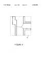
- FIG. 1illustrates the design constraints set out above.
- FIG. 1shows an area of a circuit through which passes an active metal line 89, an active metal line 91 and an active metal line 92.
- an active metal line 89an active metal line 91
- an active metal line 92an active metal line 92.
- a fill metal segment 81a fill metal segment 82, a fill metal segment 83, a fill metal segment 84, a fill metal segment 85, a fill metal segment 86, a fill metal segment 87, a fill metal segment 88 and a fill metal segment 90.
- the width (X) of a fill bar segmentis variously illustrated by an arrow 95, an arrow 98 and an arrow 101.
- the width (X) of each fill bar segment (in the short direction)is less than or equal to 1.25 times the design rule metal pitch.
- the space (Y) between each fill bar segmentis variously illustrated by an arrow 94, an arrow 96 and an arrow 97.
- the space (Y) between each fill bar segmentis greater than or equal to 0.7 times the design rule metal pitch.
- the space (Z) between any fill bar segment and an active signal lineis variously illustrated by an arrow 99, an arrow 100 and an arrow 102.
- the space (Z) between any fill bar segment and an active signal lineis greater than or equal to 0.5 times the design rule metal pitch.
- the design rule metal pitchis 2.4 micrometers.
- the width (X) of each fill bar segmentis less than or equal to 1.25 times the design rule metal pitch
- the width (X) of each fill bar segmentis less than or equal 1.25*2.4 ⁇ m, which is 3 ⁇ m.
- the space (Y) between each fill bar segmentis greater than or equal to 0.7 times the design rule metal pitch
- the space (Y) between each fill bar segmentis greater than or equal to 0.7*2.4 ⁇ m, which is 1.68 ⁇ m.
- the space (Z) between any fill bar segment and an active signal lineis greater than or equal to 0.5 times the design rule metal pitch
- the space (Z) between any fill bar segment and an active signal lineis greater than or equal to 0.5*2.4 ⁇ m, which is 1.2 ⁇ m.
- the design rule metal pitchis 2.1 micrometers.
- the width (X) of each fill bar segmentis less than or equal to 1.25 times the design rule metal pitch
- the width (X) of each fill bar segmentis less than or equal 1.25*2.1 ⁇ m, which is 2.625 ⁇ m.
- the space (Y) between each fill bar segmentis greater than or equal to 0.7 times the design rule metal pitch
- the space (Y) between each fill bar segmentis greater than or equal to 0.7*2.1 ⁇ m, which is 1.47 ⁇ m.
- the space (Z) between any fill bar segment and an active signal lineis greater than or equal to 0.5 times the design rule metal pitch
- the space (Z) between any fill bar segment and an active signal lineis greater than or equal to 0.5*2.1 ⁇ m, which is 1.05 ⁇ m.
- FIG. 2shows a herring bone pattern for metal fill used in two 10 distinct layers. Included within the first metal layer is a metal fill segment 111, metal fill segment 112, metal fill segment 113, metal fill segment 114, metal fill segment 115, metal fill segment 116, metal fill segment 117, metal fill segment 118, metal fill segment 119, metal fill segment 120, metal fill segment 121, metal fill segment 122 and metal fill segment 123. Included 15 within the second metal layer is a metal fill segment 131, metal fill segment 132, metal fill segment 133, metal fill segment 134, metal fill segment 135, metal fill segment 136, metal fill segment 137, metal fill segment 138, metal fill segment 139 and metal fill segment 140.
- the metal fillis added to a metal layer of an integrated circuit by adding a fill pattern to the active circuitry lines of a mask.
- One process which can be used to accomplished thisis set out in U.S. patent application Ser. No. 08/504,157, filed Jul. 19, 1995. This process is described below.
- a fill patternis added to the active circuitry lines of a mask in order to improve global planarization.
- a dielectric layer between a polysilicon layer and a first metal layeris planarized to facilitate pattern and etch of the first metal layer placed over the polysilicon layer.
- a dielectric layer between the first metal layer and a second metal layeris planarized to facilitate pattern and etch of the second metal layer placed over the first metal layer.
- Planarizationis achieved by placing a fill pattern on a mask for the layer that is to be planarized.
- the fill patternhas the following characteristics.
- the fill patternis made up of lines (called fill lines) and spaces comparable to those found on the circuit. Therefore, the spaces between geometries on the same layer throughout the circuit are fairly consistent. Design rules for circuitry are not violated.
- the fill linesare discontinuous at intervals to minimize the possibility of shorts.
- FIG. 3is a flowchart which summarizes steps to generate a pattern filled mask in accordance with one embodiment of the present invention.
- an active layerconsisting of active circuitry lines is generated for a mask in Manufacturing Electron Beam Exposure System (MEBES) format available from Etec Corporation of Hayward, Calif. This is done, for example, using generation software, such as Computer Aided Transcription System (CATS) available from Transcription Enterprises, Limited, having a business address of 105 Albright Way, Los Gatos, Calif. 95030.
- the active circuitry linesdetermine the pattern of a mask resulting from implementation of a circuit design before a fill pattern is added.
- FIG. 4shows a portion 20 of a pattern for a mask.
- the patternincludes active circuitry lines 21.
- a marker layeris generated to mark areas on the mask to receive the fill pattern.
- the marker layeris generated by oversizing the active circuitry lines. For example, 0.75 microns is added in each direction to the width and to the height of each active circuitry line. After oversizing the active circuitry lines, the result is inverted to produce a negative of the pattern of the oversized active circuitry lines.
- the marker layermarks areas to be filled.
- FIG. 5shows a portion 30 of a marker layer for the mask.
- the patternincludes marked areas 31 corresponding to inversion of active circuitry of FIG. 4.
- a dummy fill patternis generated, for example using a layout editor or an automated pattern generator.
- the dummy fill patternis composed of rectangles (fill lines) of predetermined length and width.
- the width of each rectangleis one micron and the height of each rectangle is ten microns.
- the rectanglesare repeated at a predetermined spacing.
- the spacing between the rectanglesis 0.75 microns in both the horizontal and the vertical directions.
- Other pattern shapesalso may be used.
- a herring bone patternis used.
- FIG. 6shows a portion 40 of a dummy fill pattern.
- the dummy fill patternis composed of rectangles 41, as shown.
- an intersection(logic AND) is performed of the marker layer generated in step 12 with the dummy fill pattern generated in step 13.
- the intersectionis done without attempting to align the dummy fill pattern with the active circuitry lines.
- the resulting unsized fill patternmay contain geometries which are smaller than the minimum size allowed by design rules.
- FIG. 7shows a portion 50 of the unsized fill pattern described above.
- the unsized fill patternincludes rectangles and rectangle portions 51 remaining after intersection.
- Step 14, for example,is also used to clip the size of the fill pattern when the dummy fill pattern covers an area larger than the area covered by the mask.
- the unsized fill pattern created in step 14is negatively sized to eliminate geometries which are smaller than the minimum size allowed by design rules.
- the resultis then resized an equal amount to restore the remaining geometries to their unsized dimensions. For example, areas that have widths or heights smaller than 1.00 microns are removed.
- the resulting patternis the pattern fill to be used on the mask.
- FIG. 8shows a portion 60 of the pattern fill resulting from the performance of step 15.
- the pattern fill shapes 61will be used to provide fill for the mask.
- a union(logic OR) of the active circuitry lines of the active layer generated in step 11 and the pattern fill shapes of the pattern fill generated in step 15 is performed.
- the results of this unionis the completed mask layer definition and defines the pattern on the mask used for patterning the layer of material used in integrated circuit manufacturing.
- FIG. 9shows a portion 70 of the pattern of the completed mask layer definition.
- the pattern of the completed mask layer definitionincludes active circuitry lines 71 and a fill pattern 72.
Landscapes
- Engineering & Computer Science (AREA)
- Physics & Mathematics (AREA)
- Computer Hardware Design (AREA)
- General Physics & Mathematics (AREA)
- Microelectronics & Electronic Packaging (AREA)
- Condensed Matter Physics & Semiconductors (AREA)
- Power Engineering (AREA)
- Geometry (AREA)
- Theoretical Computer Science (AREA)
- Manufacturing & Machinery (AREA)
- Evolutionary Computation (AREA)
- General Engineering & Computer Science (AREA)
- Internal Circuitry In Semiconductor Integrated Circuit Devices (AREA)
Abstract
Description
X<=1.25*Dp
Y>=0.7*Dp
Z>=0.5*Dp
Claims (12)
Priority Applications (1)
| Application Number | Priority Date | Filing Date | Title |
|---|---|---|---|
| US08/673,950US5763955A (en) | 1996-07-01 | 1996-07-01 | Patterned filled layers for integrated circuit manufacturing |
Applications Claiming Priority (1)
| Application Number | Priority Date | Filing Date | Title |
|---|---|---|---|
| US08/673,950US5763955A (en) | 1996-07-01 | 1996-07-01 | Patterned filled layers for integrated circuit manufacturing |
Publications (1)
| Publication Number | Publication Date |
|---|---|
| US5763955Atrue US5763955A (en) | 1998-06-09 |
Family
ID=24704737
Family Applications (1)
| Application Number | Title | Priority Date | Filing Date |
|---|---|---|---|
| US08/673,950Expired - LifetimeUS5763955A (en) | 1996-07-01 | 1996-07-01 | Patterned filled layers for integrated circuit manufacturing |
Country Status (1)
| Country | Link |
|---|---|
| US (1) | US5763955A (en) |
Cited By (43)
| Publication number | Priority date | Publication date | Assignee | Title |
|---|---|---|---|---|
| US5920487A (en)* | 1997-03-03 | 1999-07-06 | Motorola Inc. | Two dimensional lithographic proximity correction using DRC shape functions |
| US6211050B1 (en) | 1999-03-03 | 2001-04-03 | Chartered Semiconductor Manufacturing Ltd. | Fill pattern in kerf areas to prevent localized non-uniformities of insulating layers at die corners on semiconductor substrates |
| WO2000019490A3 (en)* | 1998-09-29 | 2002-01-10 | Conexant Systems Inc | Dummy fill cell for reducing layer-to-layer interaction |
| US6436807B1 (en)* | 2000-01-18 | 2002-08-20 | Agere Systems Guardian Corp. | Method for making an interconnect layer and a semiconductor device including the same |
| US6441469B1 (en)* | 1999-02-24 | 2002-08-27 | Infineon Technologies Ag | Semiconductor memory configuration with dummy components on continuous diffusion regions |
| US20020170031A1 (en)* | 2001-02-28 | 2002-11-14 | Nec Corporation | Method for manufacturing a pair of complementary masks |
| US6499135B1 (en)* | 2000-05-25 | 2002-12-24 | Sun Microsystems, Inc. | Computer aided design flow to locate grounded fill in a large scale integrated circuit |
| US6523163B1 (en)* | 1999-11-18 | 2003-02-18 | Dainippon Printing Co., Ltd. | Method for forming pattern data and method for writing a photomask with additional patterns |
| US20030168741A1 (en)* | 2001-10-24 | 2003-09-11 | Werner Juengling | Fill pattern generation for spin-on glass and related self-planarization deposition |
| US20030229880A1 (en)* | 2002-06-07 | 2003-12-11 | David White | Test masks for lithographic and etch processes |
| US20030229875A1 (en)* | 2002-06-07 | 2003-12-11 | Smith Taber H. | Use of models in integrated circuit fabrication |
| US20030228714A1 (en)* | 2002-06-07 | 2003-12-11 | Smith Taber H. | Dummy fill for integrated circuits |
| US20030226757A1 (en)* | 2002-06-07 | 2003-12-11 | Smith Taber H. | Dummy fill for integrated circuits |
| US20030229479A1 (en)* | 2002-06-07 | 2003-12-11 | Smith Taber H. | Dummy fill for integrated circuits |
| US6696359B1 (en)* | 2002-08-30 | 2004-02-24 | Micron Technology, Inc. | Design layout method for metal lines of an integrated circuit |
| US20040098393A1 (en)* | 2002-11-19 | 2004-05-20 | Cadence Design Systems, Inc. | Method, system, and article of manufacture for implementing metal-fill on an integrated circuit |
| US20040098674A1 (en)* | 2002-11-19 | 2004-05-20 | Cadence Design Systems, Inc. | Place and route tool that incorporates a metal-fill mechanism |
| US6751785B1 (en)* | 2002-03-12 | 2004-06-15 | Ubitech, Inc. | System and method for limiting increase in capacitance due to dummy metal fills utilized for improving planar profile uniformity |
| WO2003079240A3 (en)* | 2002-03-12 | 2004-07-15 | Ubitech Inc | System and method for placement of dummy metal fills while preserving device matching and/or limiting capacitance increase |
| US20040255259A1 (en)* | 2003-06-11 | 2004-12-16 | Patrick Tan | Device, design and method for a slot in a conductive area |
| US20050044520A1 (en)* | 2002-11-19 | 2005-02-24 | Cadence Design Systems, Inc. | Method, system, and article of manufacture for implementing metal-fill with power or ground connection |
| US20050098898A1 (en)* | 2003-11-06 | 2005-05-12 | Wong Robert C. | Generation of metal holes by via mutation |
| US20050132306A1 (en)* | 2002-06-07 | 2005-06-16 | Praesagus, Inc., A Massachusetts Corporation | Characterization and reduction of variation for integrated circuits |
| US20060001022A1 (en)* | 2000-03-07 | 2006-01-05 | Micron Technology, Inc. | Methods for making nearly planar dielectric films in integrated circuits |
| US20060105564A1 (en)* | 2004-11-17 | 2006-05-18 | Taravade Kunal N | Method and system for reducing inter-layer capacitance in integrated circuits |
| EP1573605A4 (en)* | 2002-11-19 | 2006-08-16 | Cadence Design Systems Inc | Method, system, and article of manufacture for implementing metal-fill |
| US20060238292A1 (en)* | 2005-04-11 | 2006-10-26 | Texas Instruments Incorporated | Thin film resistor and dummy fill structure and method to improve stability and reduce self-heating |
| US20060246609A1 (en)* | 2005-04-28 | 2006-11-02 | International Business Machines Corporation | Dynamic metal fill for correcting non-planar region |
| US20070157139A1 (en)* | 2002-06-07 | 2007-07-05 | David White | Characterization and verification for integrated circuit designs |
| US20070256039A1 (en)* | 2002-06-07 | 2007-11-01 | Cadence Design Systems, Inc. | Dummy fill for integrated circuits |
| US20080027698A1 (en)* | 2002-06-07 | 2008-01-31 | Cadence Design Systems, Inc. | Method and System for Handling Process Related Variations for Integrated Circuits Based Upon Reflections |
| US20080086714A1 (en)* | 2006-10-06 | 2008-04-10 | Faure Thomas B | Structure and method for partitioned dummy fill shapes for reduced mask bias with alternating phase shift masks |
| US20080251930A1 (en)* | 2007-04-16 | 2008-10-16 | Nec Electronics Corporation | Semiconductor device and dummy pattern arrangement method |
| US20090100399A1 (en)* | 2007-10-16 | 2009-04-16 | International Business Machines Corporation | Design structure for partitioned dummy fill shapes for reduced mask bias with alternating phase shift masks |
| US20090164959A1 (en)* | 2007-12-19 | 2009-06-25 | Nec Electronics Corporation | Layout design device and layout design method of semiconductor integrated circuit |
| US20140210098A1 (en)* | 2013-01-29 | 2014-07-31 | Christopher J. Jezewski | Techniques for enhancing fracture resistance of interconnects |
| US20150371947A1 (en)* | 2014-06-18 | 2015-12-24 | Taiwan Semiconductor Manufacturing Company, Ltd. | Devices, Packaging Devices, and Methods of Packaging Semiconductor Devices |
| US9502354B2 (en) | 2009-05-18 | 2016-11-22 | Longitude Semiconductor S.A.R.L. | Semiconductor device with layout of wiring layer and dummy patterns |
| US9831214B2 (en)* | 2014-06-18 | 2017-11-28 | Taiwan Semiconductor Manufacturing Company, Ltd. | Semiconductor device packages, packaging methods, and packaged semiconductor devices |
| US11011303B2 (en) | 2018-08-21 | 2021-05-18 | Globalfoundries U.S. Inc. | Dummy fill with eddy current self-canceling element for inductor component |
| US11056253B2 (en)* | 2019-03-18 | 2021-07-06 | Qualcomm Incorporated | Thin-film resistors with flexible terminal placement for area saving |
| US11610839B2 (en) | 2019-10-29 | 2023-03-21 | Globalfoundries U.S. Inc. | Dummy fill structures |
| US20240063119A1 (en)* | 2021-07-09 | 2024-02-22 | Taiwan Semiconductor Manufacturing Company, Ltd. | Two-dimensional (2d) metal structure |
Citations (5)
| Publication number | Priority date | Publication date | Assignee | Title |
|---|---|---|---|---|
| US5153143A (en)* | 1990-02-26 | 1992-10-06 | Delco Electronics Corporation | Method of manufacturing CMOS integrated circuit with EEPROM |
| US5210701A (en)* | 1989-05-15 | 1993-05-11 | Cascade Design Automation Corporation | Apparatus and method for designing integrated circuit modules |
| US5351197A (en)* | 1989-04-13 | 1994-09-27 | Cascade Design Automation Corporation | Method and apparatus for designing the layout of a subcircuit in an integrated circuit |
| US5654589A (en)* | 1995-06-06 | 1997-08-05 | Advanced Micro Devices, Incorporated | Landing pad technology doubled up as local interconnect and borderless contact for deep sub-half micrometer IC application |
| US5667940A (en)* | 1994-05-11 | 1997-09-16 | United Microelectronics Corporation | Process for creating high density integrated circuits utilizing double coating photoresist mask |
- 1996
- 1996-07-01USUS08/673,950patent/US5763955A/ennot_activeExpired - Lifetime
Patent Citations (5)
| Publication number | Priority date | Publication date | Assignee | Title |
|---|---|---|---|---|
| US5351197A (en)* | 1989-04-13 | 1994-09-27 | Cascade Design Automation Corporation | Method and apparatus for designing the layout of a subcircuit in an integrated circuit |
| US5210701A (en)* | 1989-05-15 | 1993-05-11 | Cascade Design Automation Corporation | Apparatus and method for designing integrated circuit modules |
| US5153143A (en)* | 1990-02-26 | 1992-10-06 | Delco Electronics Corporation | Method of manufacturing CMOS integrated circuit with EEPROM |
| US5667940A (en)* | 1994-05-11 | 1997-09-16 | United Microelectronics Corporation | Process for creating high density integrated circuits utilizing double coating photoresist mask |
| US5654589A (en)* | 1995-06-06 | 1997-08-05 | Advanced Micro Devices, Incorporated | Landing pad technology doubled up as local interconnect and borderless contact for deep sub-half micrometer IC application |
Non-Patent Citations (6)
| Title |
|---|
| D. Webb, S. Sivaram, D. Stark, H. Bath, J. Draina, R. Leggett, and R. Tolles, Complete Intermetal Planarization Using ECR Oxide and Chemical Mechanical Polish, 1992 ISMIC, pp. 141 148.* |
| D. Webb, S. Sivaram, D. Stark, H. Bath, J. Draina, R. Leggett, and R. Tolles, Complete Intermetal Planarization Using ECR Oxide and Chemical Mechanical Polish, 1992 ISMIC, pp. 141-148. |
| M. Ichikawa, et al, Multilevel Interconnect System for 0.35 m CMOS LSI s with metal dummy planarization process and thin tungsten Wirings, 1995 VMIC Conference, 1995 ISMIC, pp. 254 269.* |
| M. Ichikawa, et al, Multilevel Interconnect System for 0.35 μm CMOS LSI's with metal dummy planarization process and thin tungsten Wirings, 1995 VMIC Conference, 1995 ISMIC, pp. 254-269. |
| S. Wolf, Silicon Processing for the VLSI Era, vol. 2 Process Integration, Lattice Press 1990, pp. 229 236.* |
| S. Wolf, Silicon Processing for the VLSI Era, vol. 2--Process Integration, Lattice Press 1990, pp. 229-236. |
Cited By (122)
| Publication number | Priority date | Publication date | Assignee | Title |
|---|---|---|---|---|
| US5920487A (en)* | 1997-03-03 | 1999-07-06 | Motorola Inc. | Two dimensional lithographic proximity correction using DRC shape functions |
| WO2000019490A3 (en)* | 1998-09-29 | 2002-01-10 | Conexant Systems Inc | Dummy fill cell for reducing layer-to-layer interaction |
| US6441469B1 (en)* | 1999-02-24 | 2002-08-27 | Infineon Technologies Ag | Semiconductor memory configuration with dummy components on continuous diffusion regions |
| US6211050B1 (en) | 1999-03-03 | 2001-04-03 | Chartered Semiconductor Manufacturing Ltd. | Fill pattern in kerf areas to prevent localized non-uniformities of insulating layers at die corners on semiconductor substrates |
| US6523163B1 (en)* | 1999-11-18 | 2003-02-18 | Dainippon Printing Co., Ltd. | Method for forming pattern data and method for writing a photomask with additional patterns |
| US6436807B1 (en)* | 2000-01-18 | 2002-08-20 | Agere Systems Guardian Corp. | Method for making an interconnect layer and a semiconductor device including the same |
| US6683382B2 (en) | 2000-01-18 | 2004-01-27 | Agere Systems Inc. | Semiconductor device having an interconnect layer with a plurality of layout regions having substantially uniform densities of active interconnects and dummy fills |
| US20060001022A1 (en)* | 2000-03-07 | 2006-01-05 | Micron Technology, Inc. | Methods for making nearly planar dielectric films in integrated circuits |
| US6499135B1 (en)* | 2000-05-25 | 2002-12-24 | Sun Microsystems, Inc. | Computer aided design flow to locate grounded fill in a large scale integrated circuit |
| US20020170031A1 (en)* | 2001-02-28 | 2002-11-14 | Nec Corporation | Method for manufacturing a pair of complementary masks |
| US6647543B2 (en)* | 2001-02-28 | 2003-11-11 | Nec Corporation | Method for manufacturing a pair of complementary masks |
| US7026717B2 (en) | 2001-10-24 | 2006-04-11 | Micron Technology, Inc. | Fill pattern generation for spin-on glass and related self-planarization deposition |
| US6806577B2 (en)* | 2001-10-24 | 2004-10-19 | Micron Technology, Inc. | Fill pattern generation for spin-on glass and related self-planarization deposition |
| CN1310308C (en)* | 2001-10-24 | 2007-04-11 | 微米技术公司 | Fill pattern generation for spin-on glass and related self-planarization deposition |
| US20040155319A1 (en)* | 2001-10-24 | 2004-08-12 | Werner Juengling | Fill pattern generation for spin-on glass and related self-planarization deposition |
| US20050001322A1 (en)* | 2001-10-24 | 2005-01-06 | Werner Juengling | Fill pattern generation for spin-on glass and related self-planarization deposition |
| US6812138B2 (en)* | 2001-10-24 | 2004-11-02 | Micron Technology, Inc. | Fill pattern generation for spin-on glass and related self-planarization deposition |
| US6809389B2 (en)* | 2001-10-24 | 2004-10-26 | Micron Technology, Inc. | Fill pattern generation for spin-on glass and related self-planarization deposition |
| US20040157428A1 (en)* | 2001-10-24 | 2004-08-12 | Werner Juengling | Fill pattern generation for spin-on glass and related self-planarization deposition |
| WO2003036711A3 (en)* | 2001-10-24 | 2003-12-31 | Micron Technology Inc | Fill pattern generation for spin-on glass and related self-planarization deposition |
| US20030168741A1 (en)* | 2001-10-24 | 2003-09-11 | Werner Juengling | Fill pattern generation for spin-on glass and related self-planarization deposition |
| US6777813B2 (en)* | 2001-10-24 | 2004-08-17 | Micron Technology, Inc. | Fill pattern generation for spin-on-glass and related self-planarization deposition |
| US20040157137A1 (en)* | 2001-10-24 | 2004-08-12 | Werner Juengling | Fill pattern generation for spin-on glass and related self-planarization deposition |
| WO2003079240A3 (en)* | 2002-03-12 | 2004-07-15 | Ubitech Inc | System and method for placement of dummy metal fills while preserving device matching and/or limiting capacitance increase |
| US6904581B1 (en)* | 2002-03-12 | 2005-06-07 | Ubitech, Inc. | System and method for placement of dummy metal fills while preserving device matching and/or limiting capacitance increase |
| US6751785B1 (en)* | 2002-03-12 | 2004-06-15 | Ubitech, Inc. | System and method for limiting increase in capacitance due to dummy metal fills utilized for improving planar profile uniformity |
| US20030229479A1 (en)* | 2002-06-07 | 2003-12-11 | Smith Taber H. | Dummy fill for integrated circuits |
| US20030228714A1 (en)* | 2002-06-07 | 2003-12-11 | Smith Taber H. | Dummy fill for integrated circuits |
| US8001516B2 (en) | 2002-06-07 | 2011-08-16 | Cadence Design Systems, Inc. | Characterization and reduction of variation for integrated circuits |
| US20080027698A1 (en)* | 2002-06-07 | 2008-01-31 | Cadence Design Systems, Inc. | Method and System for Handling Process Related Variations for Integrated Circuits Based Upon Reflections |
| US7325206B2 (en) | 2002-06-07 | 2008-01-29 | Cadence Design Systems, Inc. | Electronic design for integrated circuits based process related variations |
| US7356783B2 (en) | 2002-06-07 | 2008-04-08 | Cadence Design Systems, Inc. | Dummy fill for integrated circuits |
| US20030237064A1 (en)* | 2002-06-07 | 2003-12-25 | David White | Characterization and verification for integrated circuit designs |
| US7353475B2 (en) | 2002-06-07 | 2008-04-01 | Cadence Design Systems, Inc. | Electronic design for integrated circuits based on process related variations |
| US20030229412A1 (en)* | 2002-06-07 | 2003-12-11 | David White | Electronic design for integrated circuits based on process related variations |
| US7853904B2 (en) | 2002-06-07 | 2010-12-14 | Cadence Design Systems, Inc. | Method and system for handling process related variations for integrated circuits based upon reflections |
| US20030226757A1 (en)* | 2002-06-07 | 2003-12-11 | Smith Taber H. | Dummy fill for integrated circuits |
| US20050037522A1 (en)* | 2002-06-07 | 2005-02-17 | Praesagus Inc., A Massachusetts Corporation | Dummy fill for integrated circuits |
| US7774726B2 (en) | 2002-06-07 | 2010-08-10 | Cadence Design Systems, Inc. | Dummy fill for integrated circuits |
| US20050051809A1 (en)* | 2002-06-07 | 2005-03-10 | Praesagus, Inc., A Massachusetts Corporation | Dummy fill for integrated circuits |
| US20070256039A1 (en)* | 2002-06-07 | 2007-11-01 | Cadence Design Systems, Inc. | Dummy fill for integrated circuits |
| US7757195B2 (en) | 2002-06-07 | 2010-07-13 | Cadence Design Systems, Inc. | Methods and systems for implementing dummy fill for integrated circuits |
| US7712056B2 (en) | 2002-06-07 | 2010-05-04 | Cadence Design Systems, Inc. | Characterization and verification for integrated circuit designs |
| US20030229868A1 (en)* | 2002-06-07 | 2003-12-11 | David White | Electronic design for integrated circuits based process related variations |
| US20050132306A1 (en)* | 2002-06-07 | 2005-06-16 | Praesagus, Inc., A Massachusetts Corporation | Characterization and reduction of variation for integrated circuits |
| US20050196964A1 (en)* | 2002-06-07 | 2005-09-08 | Praesagus, Inc. | Dummy fill for integrated circuits |
| US20050235246A1 (en)* | 2002-06-07 | 2005-10-20 | Praesagus, Inc., A Massachusetts Corporation | Use of models in integrated circuit fabrication |
| US7962867B2 (en) | 2002-06-07 | 2011-06-14 | Cadence Design Systems, Inc. | Electronic design for integrated circuits based on process related variations |
| US20030229875A1 (en)* | 2002-06-07 | 2003-12-11 | Smith Taber H. | Use of models in integrated circuit fabrication |
| US20090031261A1 (en)* | 2002-06-07 | 2009-01-29 | Cadence Design Systems, Inc. | Characterization and reduction of variation for integrated circuits |
| US20080216027A1 (en)* | 2002-06-07 | 2008-09-04 | Cadence Design Systems, Inc. | Electronic Design for Integrated Circuits Based on Process Related Variations |
| US7393755B2 (en) | 2002-06-07 | 2008-07-01 | Cadence Design Systems, Inc. | Dummy fill for integrated circuits |
| US7124386B2 (en) | 2002-06-07 | 2006-10-17 | Praesagus, Inc. | Dummy fill for integrated circuits |
| US7383521B2 (en) | 2002-06-07 | 2008-06-03 | Cadence Design Systems, Inc. | Characterization and reduction of variation for integrated circuits |
| US7380220B2 (en) | 2002-06-07 | 2008-05-27 | Cadence Design Systems, Inc. | Dummy fill for integrated circuits |
| US7152215B2 (en) | 2002-06-07 | 2006-12-19 | Praesagus, Inc. | Dummy fill for integrated circuits |
| US7174520B2 (en) | 2002-06-07 | 2007-02-06 | Praesagus, Inc. | Characterization and verification for integrated circuit designs |
| US7367008B2 (en) | 2002-06-07 | 2008-04-29 | Cadence Design Systems, Inc. | Adjustment of masks for integrated circuit fabrication |
| US20030229410A1 (en)* | 2002-06-07 | 2003-12-11 | Smith Taber H. | Integrated circuit metrology |
| US20070101305A1 (en)* | 2002-06-07 | 2007-05-03 | Praesagus, Inc. | Methods and systems for implementing dummy fill for integrated circuits |
| US7363099B2 (en) | 2002-06-07 | 2008-04-22 | Cadence Design Systems, Inc. | Integrated circuit metrology |
| US20030229880A1 (en)* | 2002-06-07 | 2003-12-11 | David White | Test masks for lithographic and etch processes |
| US20070157139A1 (en)* | 2002-06-07 | 2007-07-05 | David White | Characterization and verification for integrated circuit designs |
| US7243316B2 (en) | 2002-06-07 | 2007-07-10 | Praesagus, Inc. | Test masks for lithographic and etch processes |
| US7363598B2 (en) | 2002-06-07 | 2008-04-22 | Cadence Design Systems, Inc. | Dummy fill for integrated circuits |
| US7360179B2 (en) | 2002-06-07 | 2008-04-15 | Cadence Design Systems, Inc. | Use of models in integrated circuit fabrication |
| US6867498B2 (en) | 2002-08-30 | 2005-03-15 | Micron Technology, Inc. | Metal line layout of an integrated circuit |
| US20040188679A1 (en)* | 2002-08-30 | 2004-09-30 | Ireland Philip J. | Metal line layout of an integrated circuit |
| US6696359B1 (en)* | 2002-08-30 | 2004-02-24 | Micron Technology, Inc. | Design layout method for metal lines of an integrated circuit |
| US20040043591A1 (en)* | 2002-08-30 | 2004-03-04 | Ireland Philip J. | Design layout method for metal lines of an integrated circuit |
| US7231624B2 (en) | 2002-11-19 | 2007-06-12 | Cadence Design Systems, Inc. | Method, system, and article of manufacture for implementing metal-fill with power or ground connection |
| US7865858B2 (en) | 2002-11-19 | 2011-01-04 | Cadence Design Systems, Inc. | Method, system, and article of manufacture for implementing metal-fill with power or ground connection |
| US7328419B2 (en)* | 2002-11-19 | 2008-02-05 | Cadence Design Systems, Inc. | Place and route tool that incorporates a metal-fill mechanism |
| US20050044520A1 (en)* | 2002-11-19 | 2005-02-24 | Cadence Design Systems, Inc. | Method, system, and article of manufacture for implementing metal-fill with power or ground connection |
| US7287324B2 (en) | 2002-11-19 | 2007-10-30 | Cadence Design Systems, Inc. | Method, system, and article of manufacture for implementing metal-fill on an integrated circuit |
| US20070234265A1 (en)* | 2002-11-19 | 2007-10-04 | Cadence Design Systems, Inc. | Method, System, and Article of Manufacture for Implementing Metal-Fill With Power or Ground Connection |
| EP1573605A4 (en)* | 2002-11-19 | 2006-08-16 | Cadence Design Systems Inc | Method, system, and article of manufacture for implementing metal-fill |
| US20080148212A1 (en)* | 2002-11-19 | 2008-06-19 | Cadence Design Systems, Inc. | Place and Route Tool That Incorporates a Metal-Fill Mechanism |
| US8327300B2 (en)* | 2002-11-19 | 2012-12-04 | Cadence Design Systems, Inc. | Place and route tool that incorporates a metal-fill mechanism |
| US20040098393A1 (en)* | 2002-11-19 | 2004-05-20 | Cadence Design Systems, Inc. | Method, system, and article of manufacture for implementing metal-fill on an integrated circuit |
| US20040098674A1 (en)* | 2002-11-19 | 2004-05-20 | Cadence Design Systems, Inc. | Place and route tool that incorporates a metal-fill mechanism |
| US7089522B2 (en)* | 2003-06-11 | 2006-08-08 | Chartered Semiconductor Manufacturing, Ltd. | Device, design and method for a slot in a conductive area |
| US20040255259A1 (en)* | 2003-06-11 | 2004-12-16 | Patrick Tan | Device, design and method for a slot in a conductive area |
| SG137655A1 (en)* | 2003-06-11 | 2007-12-28 | Chartered Semiconductor Mfg | Device, design and method for a slot in a conductive area |
| US20070118828A1 (en)* | 2003-11-06 | 2007-05-24 | International Business Machines Corporation | Generation of metal holes by via mutation |
| US20110079921A1 (en)* | 2003-11-06 | 2011-04-07 | Wong Robert C | Generation of metal holes by via mutation |
| US7875544B2 (en) | 2003-11-06 | 2011-01-25 | Infineon Technologies Ag | Method of producing a semiconductor interconnect architecture including generation of metal holes by via mutation |
| US7188321B2 (en) | 2003-11-06 | 2007-03-06 | International Business Machines Corporation | Generation of metal holes by via mutation |
| WO2005045932A1 (en)* | 2003-11-06 | 2005-05-19 | Infineon Technologies Ag | Generation of metal holes by via mutation |
| US8378493B2 (en) | 2003-11-06 | 2013-02-19 | Infineon Technologies Ag | Generation of metal holes by via mutation |
| US20050098898A1 (en)* | 2003-11-06 | 2005-05-12 | Wong Robert C. | Generation of metal holes by via mutation |
| US7396760B2 (en)* | 2004-11-17 | 2008-07-08 | Lsi Corporation | Method and system for reducing inter-layer capacitance in integrated circuits |
| US8015540B2 (en) | 2004-11-17 | 2011-09-06 | Lsi Corporation | Method and system for reducing inter-layer capacitance in integrated circuits |
| US20060105564A1 (en)* | 2004-11-17 | 2006-05-18 | Taravade Kunal N | Method and system for reducing inter-layer capacitance in integrated circuits |
| US20080235643A1 (en)* | 2004-11-17 | 2008-09-25 | Lsi Logic Corporation | Method and system for reducing inter-layer capacitance in integrated circuits |
| US20060238292A1 (en)* | 2005-04-11 | 2006-10-26 | Texas Instruments Incorporated | Thin film resistor and dummy fill structure and method to improve stability and reduce self-heating |
| US7403094B2 (en)* | 2005-04-11 | 2008-07-22 | Texas Instruments Incorporated | Thin film resistor and dummy fill structure and method to improve stability and reduce self-heating |
| US7368302B2 (en) | 2005-04-28 | 2008-05-06 | International Business Machines Corporation | Dynamic metal fill for correcting non-planar region |
| US20060246609A1 (en)* | 2005-04-28 | 2006-11-02 | International Business Machines Corporation | Dynamic metal fill for correcting non-planar region |
| US20080086714A1 (en)* | 2006-10-06 | 2008-04-10 | Faure Thomas B | Structure and method for partitioned dummy fill shapes for reduced mask bias with alternating phase shift masks |
| US7709300B2 (en) | 2006-10-06 | 2010-05-04 | International Business Machines Corporation | Structure and method for partitioned dummy fill shapes for reduced mask bias with alternating phase shift masks |
| US20080251930A1 (en)* | 2007-04-16 | 2008-10-16 | Nec Electronics Corporation | Semiconductor device and dummy pattern arrangement method |
| US7761833B2 (en)* | 2007-04-16 | 2010-07-20 | Nec Electronics Corporation | Semiconductor device and dummy pattern arrangement method |
| US7861208B2 (en) | 2007-10-16 | 2010-12-28 | International Business Machines Corporation | Structure for partitioned dummy fill shapes for reduced mask bias with alternating phase shift masks |
| US20090100399A1 (en)* | 2007-10-16 | 2009-04-16 | International Business Machines Corporation | Design structure for partitioned dummy fill shapes for reduced mask bias with alternating phase shift masks |
| US20090164959A1 (en)* | 2007-12-19 | 2009-06-25 | Nec Electronics Corporation | Layout design device and layout design method of semiconductor integrated circuit |
| US9911699B2 (en) | 2009-05-18 | 2018-03-06 | Longitude Semiconductor S.A.R.L. | Semiconductor device |
| US9508650B2 (en) | 2009-05-18 | 2016-11-29 | Longitude Semiconductor S.A.R.L. | Semiconductor device with layout of wiring layer and dummy patterns |
| US11011471B2 (en) | 2009-05-18 | 2021-05-18 | Longitude Licensing Limited | Semiconductor device |
| US9502354B2 (en) | 2009-05-18 | 2016-11-22 | Longitude Semiconductor S.A.R.L. | Semiconductor device with layout of wiring layer and dummy patterns |
| US20140210098A1 (en)* | 2013-01-29 | 2014-07-31 | Christopher J. Jezewski | Techniques for enhancing fracture resistance of interconnects |
| US9691716B2 (en) | 2013-01-29 | 2017-06-27 | Intel Corporation | Techniques for enhancing fracture resistance of interconnects |
| US9343411B2 (en)* | 2013-01-29 | 2016-05-17 | Intel Corporation | Techniques for enhancing fracture resistance of interconnects |
| US9831214B2 (en)* | 2014-06-18 | 2017-11-28 | Taiwan Semiconductor Manufacturing Company, Ltd. | Semiconductor device packages, packaging methods, and packaged semiconductor devices |
| US20150371947A1 (en)* | 2014-06-18 | 2015-12-24 | Taiwan Semiconductor Manufacturing Company, Ltd. | Devices, Packaging Devices, and Methods of Packaging Semiconductor Devices |
| US10177032B2 (en)* | 2014-06-18 | 2019-01-08 | Taiwan Semiconductor Manufacturing Company, Ltd. | Devices, packaging devices, and methods of packaging semiconductor devices |
| US11011303B2 (en) | 2018-08-21 | 2021-05-18 | Globalfoundries U.S. Inc. | Dummy fill with eddy current self-canceling element for inductor component |
| US11056253B2 (en)* | 2019-03-18 | 2021-07-06 | Qualcomm Incorporated | Thin-film resistors with flexible terminal placement for area saving |
| US11424054B2 (en) | 2019-03-18 | 2022-08-23 | Qualcomm Incorporated | Thin-film resistors with flexible terminal placement for area saving |
| US11610839B2 (en) | 2019-10-29 | 2023-03-21 | Globalfoundries U.S. Inc. | Dummy fill structures |
| US20240063119A1 (en)* | 2021-07-09 | 2024-02-22 | Taiwan Semiconductor Manufacturing Company, Ltd. | Two-dimensional (2d) metal structure |
| US12300609B2 (en)* | 2021-07-09 | 2025-05-13 | Taiwan Semiconductor Manufacturing Company, Ltd. | Two-dimensional (2D) metal structure and method of forming the same |
Similar Documents
| Publication | Publication Date | Title |
|---|---|---|
| US5763955A (en) | Patterned filled layers for integrated circuit manufacturing | |
| US5597668A (en) | Patterned filled photo mask generation for integrated circuit manufacturing | |
| KR100722177B1 (en) | Processing to Design Semiconductor Devices and Masks | |
| US6486066B2 (en) | Method of generating integrated circuit feature layout for improved chemical mechanical polishing | |
| US5854125A (en) | Dummy fill patterns to improve interconnect planarity | |
| US6709880B2 (en) | Semiconductor device and a manufacturing method of the same | |
| US5077234A (en) | Planarization process utilizing three resist layers | |
| TWI226696B (en) | Method of forming an integrated circuit device using dummy features and structure thereof | |
| TWI278014B (en) | Method of manufacturing semiconductor device | |
| US6327695B1 (en) | Automated design of on-chip capacitive structures for suppressing inductive noise | |
| US7868427B2 (en) | Structure and method for placement, sizing and shaping of dummy structures | |
| US5861342A (en) | Optimized structures for dummy fill mask design | |
| US5696406A (en) | Semiconductor device and method for fabricating the same | |
| US5618757A (en) | Method for improving the manufacturability of the spin-on glass etchback process | |
| DE102014119153A1 (en) | A method of forming various structures in a semiconductor structure using a single mask | |
| JP2000349145A (en) | Semiconductor device | |
| JP3645142B2 (en) | Semiconductor wafer processing method and semiconductor device manufacturing method | |
| US20070155126A1 (en) | Method for manufacturing semiconductor device with overlay vernier | |
| US6613688B1 (en) | Semiconductor device and process for generating an etch pattern | |
| JP3428556B2 (en) | Mask data generation method, mask, and computer-readable recording medium | |
| US6094812A (en) | Dishing avoidance in wide soft metal wires | |
| JP3334339B2 (en) | Semiconductor device wiring layout method and manufacturing method | |
| EP0982774A2 (en) | Avoidance of cross-sectional surface reduction in wide soft metal wires | |
| JP3782904B2 (en) | Manufacturing method of semiconductor integrated circuit or electronic package | |
| Nelson | Optimized pattern fill process for improved CMP uniformity and interconnect capacitance |
Legal Events
| Date | Code | Title | Description |
|---|---|---|---|
| AS | Assignment | Owner name:VLSI TECHNOLOGY, INC., CALIFORNIA Free format text:ASSIGNMENT OF ASSIGNORS INTEREST;ASSIGNORS:FINDLEY, PAUL RAJ;SMITH, MORGAN;REEL/FRAME:008083/0363 Effective date:19960626 | |
| STCF | Information on status: patent grant | Free format text:PATENTED CASE | |
| FEPP | Fee payment procedure | Free format text:PAYOR NUMBER ASSIGNED (ORIGINAL EVENT CODE: ASPN); ENTITY STATUS OF PATENT OWNER: LARGE ENTITY | |
| FPAY | Fee payment | Year of fee payment:4 | |
| FPAY | Fee payment | Year of fee payment:8 | |
| AS | Assignment | Owner name:PHILIPS SEMICONDUCTORS VLSI INC., NEW YORK Free format text:CHANGE OF NAME;ASSIGNOR:VLSI TECHNOLOGY, INC.;REEL/FRAME:018635/0570 Effective date:19990702 Owner name:NXP B.V., NETHERLANDS Free format text:ASSIGNMENT OF ASSIGNORS INTEREST;ASSIGNOR:PHILIPS SEMICONDUCTORS INC.;REEL/FRAME:018645/0779 Effective date:20061130 | |
| AS | Assignment | Owner name:PHILIPS SEMICONDUCTORS INC., NEW YORK Free format text:CHANGE OF NAME;ASSIGNOR:PHILIPS SEMICONDUCTORS VLSI INC.;REEL/FRAME:018668/0255 Effective date:19991220 | |
| AS | Assignment | Owner name:MORGAN STANLEY SENIOR FUNDING, INC., ENGLAND Free format text:SECURITY AGREEMENT;ASSIGNOR:NXP B.V.;REEL/FRAME:018806/0201 Effective date:20061201 | |
| FPAY | Fee payment | Year of fee payment:12 | |
| AS | Assignment | Owner name:NXP B.V., NETHERLANDS Free format text:RELEASE BY SECURED PARTY;ASSIGNOR:MORGAN STANLEY SENIOR FUNDING, INC;REEL/FRAME:050315/0443 Effective date:20190903 |