US5763924A - Circuits and methods for compensating non-linear capacitances to minimize harmonic distortion - Google Patents
Circuits and methods for compensating non-linear capacitances to minimize harmonic distortionDownload PDFInfo
- Publication number
- US5763924A US5763924AUS08/647,361US64736196AUS5763924AUS 5763924 AUS5763924 AUS 5763924AUS 64736196 AUS64736196 AUS 64736196AUS 5763924 AUS5763924 AUS 5763924A
- Authority
- US
- United States
- Prior art keywords
- transistor
- drain
- bias voltage
- source
- terminal
- Prior art date
- Legal status (The legal status is an assumption and is not a legal conclusion. Google has not performed a legal analysis and makes no representation as to the accuracy of the status listed.)
- Expired - Lifetime
Links
- 238000000034methodMethods0.000titleclaimsabstractdescription26
- 230000003071parasitic effectEffects0.000claimsabstractdescription73
- 230000000295complement effectEffects0.000claimsabstractdescription6
- 239000003990capacitorSubstances0.000claimsdescription18
- NWONKYPBYAMBJT-UHFFFAOYSA-Lzinc sulfateChemical compound[Zn+2].[O-]S([O-])(=O)=ONWONKYPBYAMBJT-UHFFFAOYSA-L0.000abstract1
- 239000000758substrateSubstances0.000description27
- 238000010586diagramMethods0.000description7
- XUIMIQQOPSSXEZ-UHFFFAOYSA-NSiliconChemical compound[Si]XUIMIQQOPSSXEZ-UHFFFAOYSA-N0.000description5
- 238000004519manufacturing processMethods0.000description5
- 229910052710siliconInorganic materials0.000description5
- 239000010703siliconSubstances0.000description5
- 239000002184metalSubstances0.000description3
- 229910044991metal oxideInorganic materials0.000description3
- 150000004706metal oxidesChemical class0.000description3
- 239000004065semiconductorSubstances0.000description3
- 230000008901benefitEffects0.000description2
- 230000002301combined effectEffects0.000description2
- 238000009792diffusion processMethods0.000description2
- 229910021420polycrystalline siliconInorganic materials0.000description2
- 229920005591polysiliconPolymers0.000description2
- 230000001960triggered effectEffects0.000description2
- 230000000694effectsEffects0.000description1
- 230000005684electric fieldEffects0.000description1
- 230000005669field effectEffects0.000description1
- 239000007943implantSubstances0.000description1
- 238000002513implantationMethods0.000description1
- 238000002955isolationMethods0.000description1
- 230000004048modificationEffects0.000description1
- 238000012986modificationMethods0.000description1
Images


Classifications
- G—PHYSICS
- G11—INFORMATION STORAGE
- G11C—STATIC STORES
- G11C27/00—Electric analogue stores, e.g. for storing instantaneous values
- G11C27/02—Sample-and-hold arrangements
- G—PHYSICS
- G11—INFORMATION STORAGE
- G11C—STATIC STORES
- G11C27/00—Electric analogue stores, e.g. for storing instantaneous values
- G11C27/02—Sample-and-hold arrangements
- G11C27/024—Sample-and-hold arrangements using a capacitive memory element
- H—ELECTRICITY
- H10—SEMICONDUCTOR DEVICES; ELECTRIC SOLID-STATE DEVICES NOT OTHERWISE PROVIDED FOR
- H10D—INORGANIC ELECTRIC SEMICONDUCTOR DEVICES
- H10D84/00—Integrated devices formed in or on semiconductor substrates that comprise only semiconducting layers, e.g. on Si wafers or on GaAs-on-Si wafers
- H10D84/80—Integrated devices formed in or on semiconductor substrates that comprise only semiconducting layers, e.g. on Si wafers or on GaAs-on-Si wafers characterised by the integration of at least one component covered by groups H10D12/00 or H10D30/00, e.g. integration of IGFETs
- H10D84/811—Combinations of field-effect devices and one or more diodes, capacitors or resistors
- H—ELECTRICITY
- H10—SEMICONDUCTOR DEVICES; ELECTRIC SOLID-STATE DEVICES NOT OTHERWISE PROVIDED FOR
- H10D—INORGANIC ELECTRIC SEMICONDUCTOR DEVICES
- H10D84/00—Integrated devices formed in or on semiconductor substrates that comprise only semiconducting layers, e.g. on Si wafers or on GaAs-on-Si wafers
- H10D84/80—Integrated devices formed in or on semiconductor substrates that comprise only semiconducting layers, e.g. on Si wafers or on GaAs-on-Si wafers characterised by the integration of at least one component covered by groups H10D12/00 or H10D30/00, e.g. integration of IGFETs
- H10D84/82—Integrated devices formed in or on semiconductor substrates that comprise only semiconducting layers, e.g. on Si wafers or on GaAs-on-Si wafers characterised by the integration of at least one component covered by groups H10D12/00 or H10D30/00, e.g. integration of IGFETs of only field-effect components
- H10D84/83—Integrated devices formed in or on semiconductor substrates that comprise only semiconducting layers, e.g. on Si wafers or on GaAs-on-Si wafers characterised by the integration of at least one component covered by groups H10D12/00 or H10D30/00, e.g. integration of IGFETs of only field-effect components of only insulated-gate FETs [IGFET]
- H10D84/85—Complementary IGFETs, e.g. CMOS
Definitions
- This inventionrelates to parasitic capacitances of transistor junctions, particularly in track and hold (T/H) circuits and other circuits which may incorporate T/H circuits. More specifically, the present invention relates to circuits and methods for minimizing non-linear capacitances in T/H and other circuits.
- T/H circuitsmay be used to maintain a constant magnitude output representing an input, for example in an analog-to-digital converter (ADC).
- ADCanalog-to-digital converter
- the T/H circuittypically operates in two different modes, “tracking mode” and “hold mode.” In tracking mode, the T/H circuit generally acts as an input voltage follower. In hold mode, the T/H circuit retains as an output signal the input signal voltage level at the time hold mode is initiated. The T/H circuit is typically switched between modes by simply toggling a trigger. When the T/H circuit is triggered back to tracking mode, the T/H circuit output resumes following the input voltage.
- a simple T/H circuitmay be created using a metal oxide semiconductor (NOS) transistor and a capacitor.
- NOSmetal oxide semiconductor
- One limitation with such simple MOS transistor T/H circuitsis that parasitic capacitances of transistor junctions vary non-linearly with the voltage across the transistor junctions. The parasitic capacitances are particularly troublesome during tracking mode operations, when the transistor is on and the input voltage changes cause the capacitance to vary. The varying parasitic junction capacitances interact with the remainder of the MOS transistor T/H circuit, causing harmonic distortion in the output of the T/H circuit.
- One known solution to the parasitic capacitance problemis to provide additional circuitry to keep a constant reverse bias across the parasitic diodes that effectively form between ground and the source and drain of the transistor.
- Some of these T/H circuitsemploy an operational amplifier to prevent a voltage difference across the transistor junctions, thereby linearizing the parasitic junction capacitances.
- this modificationsuffer the disadvantages of requiring more space and increased cost, but this technique also can only be used in conjunction with process technology that allows connection access to the "anode" of the parasitic diode that effectively forms between the transistor junctions and ground.
- diodesare coupled between a bias voltage and the source and drain of the transistor.
- the additional diodesact to linearize the parasitic capacitance such that the total capacitance remains relatively constant.
- two complementary transistorsare coupled together (i.e., one being p-channel and one being n-channel) such that the parasitic capacitance of each transistor linearizes the parasitic capacitance of the other transistor.
- FIG. 1is a simplified schematic diagram of a known track and hold circuit
- FIG. 2is a graph illustrating a typical operational profile of the track and hold circuit of FIG. 1;
- FIG. 3is a cross-sectional view of a conventional integrated circuit structure for an n-channel MOSFET
- FIG. 4is a graph illustrating transistor junction parasitic capacitance as a function of voltage across the transistor junction for the track and hold circuit of FIG. 1;
- FIG. 5is a schematic diagram of a prior art track and hold circuit, employing an operational amplifier for linearizing transistor junction parasitic capacitances
- FIG. 6is a schematic diagram of one embodiment of a parasitic-junction-capacitance-compensated track and hold circuit, in accordance with the principles of the present invention.
- FIG. 7is a graph illustrating the combined effect of transistor junction parasitic capacitance and compensating junction capacitance, in accordance with the principles of the present invention.
- FIG. 8is a cross-sectional view of an integrated circuit structure for a parasitic-junction-capacitance-compensated n-channel MOSFET, in accordance with the principles of the present invention.
- FIG. 9is a schematic diagram of another embodiment of a parasitic-capacitance-compensated track and hold circuit and method, in accordance with the principles of the present invention.
- T/H circuitsincorporating the junction-capacitance compensating principles of the present invention are described below.
- the T/H circuits providedare low-cost and accurate, due in part to the techniques that compensate for the transistor junction parasitic capacitances without requiring complicated additional circuitry (e.g., amplifiers).
- the compensation of the provided T/H circuitdoes not require that a particular process technology be employed.
- FIG. 1is a simplified schematic diagram of a known T/H circuit.
- a known T/H circuit 100employing a metal oxide semiconductor (MOS) transistor 102, and a capacitor 104 is shown.
- Resistor 106represents the input source impedance.
- MOS transistor 102also includes parasitic junction capacitances that are represented by PJC diodes 112 and 114 at the drain and source, respectively, of MOS transistor 102.
- PJC diodes 112 and 114are enclosed in dashed boxes to indicate that rather than being separate components, they represent the p-n junctions of MOS transistor 102.
- an input signal V INcauses the voltage at input node 108 to vary.
- MOS transistor 102When the gate of MOS transistor 102 is coupled to a voltage greater than the voltage at input node 108, MOS transistor 102 is on and behaves like a resistor--allowing capacitor 104 to charge and discharge so that the output V OUT at output node 110 follows the input signal V IN (i.e., tracking mode).
- MOS transistor 102When the gate of MOS transistor 102 is coupled to a voltage less than the voltage at input node 108, MOS transistor 102 is off--isolating the input signal V IN from capacitor 104 and output node 110 so that output V OUT at output node 110 remains constant at the value of V IN prior to switching modes (i.e., hold mode).
- a signal V TRIGGER at the gate of MOS transistor 102may serve as a trigger between operation of T/H circuit 100 in tracking mode and hold mode.
- FIG. 2illustrates one ideal operation of T/H circuit 100.
- input signal V IN 200varies over time.
- trigger signal V TRIGGER 202is briefly toggled above input signal V IN 200.
- Output signal V OUT 204follows input signal V IN 200 while trigger signal V TRIGGER 202 exceeds input signal V IN 200, and holds constant at the last value of input-signal V IN 200 when trigger signal V TRIGGER 202 is brought below input signal V IN 200.
- T/H circuit 100 of FIG. 1suffers the disadvantage of harmonic distortion due to parasitic capacitances of the junctions in MOS transistor 102, as described above. These problems are particularly troublesome for integrated circuit T/H circuits.
- FIG. 3depicts a cross-sectional view of a conventional integrated circuit structure for an n-channel metal oxide semiconductor field effect transistor (MOSFET) 300, which could be used as MOS transistor 102 in FIG. 1.
- MOSFETmetal oxide semiconductor field effect transistor
- n+-regions 302 and 304are diffused or implanted into p-type silicon substrate 306.
- Oxide layer 308is above p-type substrate 306.
- a thin portion of oxide layer 308separates polysilicon gate 320 of MOSFET 300 from p-type silicon substrate 306.
- Metal terminals 330 and 340are coupled to n+-regions 302 and 304, respectively.
- terminals 30 and 340the terminal connected to the n+-region 302 or 304 supplying the majority carrier of the channel of MOSFET 300 (which is the more negative terminal for an n-channel device) is typically designated the source (S), and the other terminal is designated the drain (D), although this designation is arbitrary with respect to terminals 330 and 340 in FIG. 3.
- Ssource
- Ddrain
- gate 320controls the flow of current between source terminal 330 and drain terminal 340 by generating an electric field in channel 310 between source n+-region 302 and drain n+-region 304. This field is produced by applying a voltage at gate 320.
- Substrate 306is often coupled to ground to avoid forward biasing either of the substrate-source ant substrate-drain p-n junctions.
- one source of parasitic capacitance in MOSFET 300is the junction between the drain n+-region 302 and the grounded p-type substrate 306.
- another source of parasitic capacitanceis the junction between the source n+-region 304 and the grounded p-type substrate 306.
- FIG. 4is a graph illustrating the parasitic junction capacitances of either of the drain-substrate or source-substrate junctions as a function of the reverse bias voltage across the respective junction.
- the voltage-variable parasitic junction capacitancesare depicted by PJC diodes 112 and 114.
- input signal V IN at input node 108changes the voltage across PJC diodes 112 and 114, causing the parasitic junction capacitances represented by PJC diodes 112 and 114 to vary.
- the voltage-varying parasitic junction capacitancesinteract with the source impedance represented by resistor 106 an; the resistance formed by MOS transistor 102 being on, causing harmonic distortion in output V OUT at output node 110.
- some known circuitsemploy an operational amplifier (op-amp) to prevent a voltage difference from being established across the drain-substrate and source-substrate transistor junctions.
- op-ampoperational amplifier
- FIG. 5show one such prior art T/H circuit 500 which uses op-amp 520 to linearize parasitic junction capacitances by preventing a voltage difference across the transistor junctions.
- T/H circuit 500requires access to the "anode" of PJC diodes 512 and 514 for connection of op-amp 520.
- Such a requirementlimits the processes available to manufacture such a circuit, as many processes produce integrated circuits in which the substrate or other "anode" of the transistor junctions may not be accessed.
- CMOS processesn-well and p-well.
- n-well CMOSFor an n-channel transistor, n-well CMOS produces a p-type substrate common to the whole integrated circuit (i.e., other circuit elements). The p-type substrate is the "anode" of the n-channel transistor junctions. Alternatively, p-well CMOS produces a p-type well in an n-type substrate.
- the p-type sellmay be the "substrate" for an n-channel transistor formed by adding n + regions to the p-type well.
- the p-type well, the "anode” of the n-channel transistor junctions,is not common to the whole integrated circuit. Accordingly, access to the "anode” of an n-channel transistor is possible in p-well CMOS, but not n-well CMOS technology. Likewise, persons skilled in the art will recognize that for p-channel transistors, access to the "anode” is possible in n-well CMOS, but not p-well CMOS technology.
- T/H circuit 500 of FIG. 5is that the inclusion of op-amp 520 on an integrated circuit requires significant space and components, which translates to increased cost.
- MOS transistor 502 and capacitor 504are substantially like, and behave substantially like MOS transistor 102 and capacitor 104 described in connection with FIGS. 1-3.
- resistor 506represents the input source impedance in FIG. 5.
- the MOS transistor 502 for T/H circuit 500 in FIG. 5is in a p-well and does not need to be grounded to prevent forward biasing of the transistor junctions, unlike p-type substrate 306 of FIG. 3. Instead, the substrate (p-well) of T/H circuit 500 in FIG. 5 is coupled to output terminal 524 of op-amp 520 and to negative input terminal 526 of op-amp 520, Positive input terminal 522 of op-amp 520 is coupled to input node 508.
- parasitic junction capacitances of MOS transistor 502 of FIG. 5are depicted by PJC diodes 512 and 514, which are enclosed by dashed boxes on FIG. 5 to show that they are not actual circuit components.
- MOS transistor 502behaves as a resistor, and op-amp 520 operates to eliminate voltage across PJC diodes 512 and 514. Accordingly, the voltage-variable parasitic capacitance of the source-substrate and drain-substrate junctions of MOS transistor 502 is linearized.
- FIG. 6provides a schematic diagram of a low-cost, parasitic-junction-capacitance-compensated T/H circuit, which does not require specific manufacturing processes that allow connection to the substrate or other "anode" of the transistor junctions.
- a T/H circuit 600 employing MOS transistor 602, and a capacitor 604is shown.
- Voltage-variable parasitic junction capacitances of MOS transistor 602are represented by PJC diodes 612 and 614 at the drain and source of MOS transistor 602.
- PJC diodes 612 and 614are enclosed in dashed boxes in FIG. 6 to indicate that rather than being separate components, they represent the p-n junctions of MOS transistor 602.
- resistor 606represents the input source impedance in FIG. 6.
- First and second compensation junction capacitance (“CJC”) diodes 622 and 624are coupled between input node 608 and bias voltage node 620, and output node 610 and bias voltage node 620, respectively.
- CJCcompensation junction capacitance
- the anode of CJC diode 622is coupled to input node 608, and the cathode of CJC diode 622 is coupled to bias voltage node 620. Likewise, the anode and cathode of CJC diode 624 are coupled to output node 610 and voltage bias node 620, respectively.
- an input signal V INcauses the voltage at input node 608 to vary.
- MOS transistor 602When the gate of MOS transistor 602 is coupled to a voltage greater than the voltage at input node 608, MOS transistor 602 is on and behaves like a resistor--allowing capacitor 604 to charge and discharge so that the output V OUT at output node 610 follows the input signal V IN (i.e., tracking mode).
- MOS transistor 602When the gate of the MOS transistor 602 is coupled to a voltage less than the voltage at input node 608, MOS transistor 602 is off--isolating the input signal V IN from capacitor 604 and output node 610 so that output V OUT at output node 610 remains constant (i.e., hold mode).
- a signal V TRIGGER at the gate of MOS transistor 602may serve as a trigger between operation of T/H circuit 600 in tracking mode and hold mode.
- FIG. 7is a graph illustrating the combined effect of the transistor junction parasitic capacitance and the compensating junction capacitance in accordance with the principles of the present invention.
- curve 702represents the parasitic junction capacitance of either of PJC diodes 612 or 614 as a function of varying voltage at input node 608 across the transistor junction.
- Curve 704represents the parasitic junction capacitance of either of CJC diodes 622 or 624 as a function of varying voltage at input node 608.
- the two voltage-variable capacitances curves 702 and 704combine to yield total capacitance curve 706, which is relatively constant over varying voltage at input node 608.
- This linearization of the parasitic junction capacitancesgreatly improves the harmonic distortion at output node 610 when MOS transistor 602 is on. And, this linearization of the parasitic junction capacitances is not limited to manufacturing processes which permit access to the substrate or other "anode" of the transistor junctions.
- FIG. 8is a cross-sectional view of an integrated circuit structure for parasitic-junction-capacitance-compensating an n-channel MOSFET, in accordance with the principles of the present invention.
- FIG. 8a cross-sectional view of an integrated circuit for parasitic-junction-capacitance-compensating MOSFET 800, which could be used as MOS transistor 602 in FIG. 6, is shown.
- n+-regions 802 and 804are diffused or implanted into p-type silicon substrate 806.
- Oxide layer 808is above p-type substrate 806.
- a thin portion of oxide layer 808separates polysilicon gate 820 of MOSFET 800 from p-type silicon substrate 806.
- Metal terminals 830 and 840are coupled to n+-regions 802 and 804 respectively.
- each of the CJC diodes 850is diffused or implanted into p-type silicon substrate 806.
- N+-region 852 and p+-region 854are diffused or implanted into n-well 850.
- Metal terminals 856 and 858are coupled to n+-region 852 and p+-region 854, respectively, for connection to bias voltage.
- either of the CJC diodesmay be formed by using the source/drain diffusions or implants of p-channel transistor 860. To do so, however, p-channel transistor 860 must be turned off.
- FIG. 9is a schematic diagram of an alternate embodiment of a parasitic-capacitance-compensated T/H circuit 900 constructed in accordance with the principles of the present invention.
- MOS transistors 901 and 902are complimentary in conductivity and are coupled at their drains and sources.
- Capacitor 904is coupled to the drains of MOS transistors 901 and 902.
- Resistor 906represents the input source impedance of T/H circuit 900.
- Parasitic junction capacitances of MOS transistors 901 and 902are represented by PJC diodes 911 and 913 and 912 and 914, respectively.
- PJC diodes 911, 912, 913 and 914are enclosed in dashed boxes to indicate that rather than being separate components, they represent the p-n junctions of MOS transistors 901 and 902.
- T/H circuit 900two complementary pairs of PJC diodes (911 and 912, 913 and 914) are present in T/H circuit 900 that, in accordance with the principles of the present invention, have offsetting effects.
- one or more compensation junction capacitance (“CJC") diode(s) 922may also be added to T/H circuit 900 to further linearize parasitic junction capacitances.
- CJC diodes 922may, for example, be added as needed: (1) between the source of MOS transistor 902 and bias voltage node 920; (2) between the drain of MOS transistor 902 and bias voltage node 920; or (3) one CJC diode 922 each between the source and drain of MOS transistor 902 and bias voltage node 920.
- the anode of a first CJC diode 922may be coupled to the source of MOS transistor 902, and the cathode of first CJC diode 922 to bias voltage node 920.
- the anode of a second CJC diode 922may be coupled to the drain of MOS transistor 902, and the cathode of second CJC diode 922 to bias voltage node 920.
- first and second CJC diodes 922may be coupled between ground and the drain or source of MOS transistor 901 (not shown on FIG. 9).
- the parasitic junction capacitances of the circuitmay be linearized to improve harmonic distortion at output node 910. And, this linearization of parasitic-junction capacitances is not limited to manufacturing processes which permit access to the substrate or other anode of the transistor-junctions.
- an input signal V INcauses the voltage at input node 908 to vary.
- the switch comprised of MOS transistors 901 and 902is on and behaves like a resistor--allowing capacitor 904 to charge and discharge so that the output V OUT at output node 910 follows the input signal V IN (i.e., tracking mode).
- the switch comprised of MOS transistors 901 and 902is off-isolating the input signal V IN from capacitor 904 and output node 910 so that output V OUT at output node 910 remains constant (i.e., hold mode).
- signals V TRIGGER1 and V TRIGGER2 at the gates of MOS transistors 901 and 902may serve as a trigger between operation of T/H circuit 900 in tracking mode and hold mode.
- the parasitic junction capacitances represented by PJC diodes 911 and 913works to linearize parasitic junction capacitances represented by PJC diodes 912 and 914. Also, by selecting the appropriate size for CJC diodes 922, as needed, the net parasitic junction capacitances can be further linearized.
- the present inventionhas been discussed above with reference to FIGS. 6-9, wherein the T/H circuit transistor comprises a MOSFET transistor, the present invention is applicable to other circuit configurations and types of input devices as well.
- a JFETmay be employed instead of a MOSFET.
- p-channel or n-channel MOSFETs or JFETsmay be used.
Landscapes
- Amplifiers (AREA)
Abstract
Description
This invention relates to parasitic capacitances of transistor junctions, particularly in track and hold (T/H) circuits and other circuits which may incorporate T/H circuits. More specifically, the present invention relates to circuits and methods for minimizing non-linear capacitances in T/H and other circuits.
T/H circuits may be used to maintain a constant magnitude output representing an input, for example in an analog-to-digital converter (ADC). Thus, the characteristics of the T/H circuit may be crucial to system accuracy, including the accuracy of any digital data created by an ADC. The T/H circuit typically operates in two different modes, "tracking mode" and "hold mode." In tracking mode, the T/H circuit generally acts as an input voltage follower. In hold mode, the T/H circuit retains as an output signal the input signal voltage level at the time hold mode is initiated. The T/H circuit is typically switched between modes by simply toggling a trigger. When the T/H circuit is triggered back to tracking mode, the T/H circuit output resumes following the input voltage.
There are many known T/H circuits. For example, a simple T/H circuit may be created using a metal oxide semiconductor (NOS) transistor and a capacitor. One limitation with such simple MOS transistor T/H circuits is that parasitic capacitances of transistor junctions vary non-linearly with the voltage across the transistor junctions. The parasitic capacitances are particularly troublesome during tracking mode operations, when the transistor is on and the input voltage changes cause the capacitance to vary. The varying parasitic junction capacitances interact with the remainder of the MOS transistor T/H circuit, causing harmonic distortion in the output of the T/H circuit.
One known solution to the parasitic capacitance problem is to provide additional circuitry to keep a constant reverse bias across the parasitic diodes that effectively form between ground and the source and drain of the transistor. Some of these T/H circuits employ an operational amplifier to prevent a voltage difference across the transistor junctions, thereby linearizing the parasitic junction capacitances. However, not only does this modification suffer the disadvantages of requiring more space and increased cost, but this technique also can only be used in conjunction with process technology that allows connection access to the "anode" of the parasitic diode that effectively forms between the transistor junctions and ground.
In view of the foregoing, it would be desirable to provide a simple, low-cost circuit that linearzes the parasitic capacitances of transistor junctions, particularly in simple T/H circuits.
It would also be desirable to provide a circuit that linearizes the parasitic capacitances of transistor junctions without requiring the use of a particular process technology.
It would be additionally desirable to provide methods for compensating non-linear capacitances to minimize harmonic distortion in both T/H circuits and non T/H circuits.
It is therefore an object of the invention to provide simple, low-cost circuits that linearizes the parasitic capacitances of transistor junctions, particularly in simple T/H circuits.
It is another object of the invention to provide circuits that linearizes the parasitic capacitances of transistor junctions without requiring the use of a particular process technology.
It is still another object of the invention to provide methods for compensating non-linear capacitances to minimize harmonic distortion in both T/H circuits and non T/H circuits.
In accordance with these and other objects of the invention, simple, low-cost circuits that linearize parasitic capacitance of transistor junctions, which are independent of process technology used, are provided. In one embodiment of the present invention, diodes are coupled between a bias voltage and the source and drain of the transistor. The additional diodes act to linearize the parasitic capacitance such that the total capacitance remains relatively constant. In another embodiment, two complementary transistors are coupled together (i.e., one being p-channel and one being n-channel) such that the parasitic capacitance of each transistor linearizes the parasitic capacitance of the other transistor.
The above and other objects of the present invention will be apparent upon consideration of the following detailed description taken in conjunction with the accompanying drawings, in which:
FIG. 1 is a simplified schematic diagram of a known track and hold circuit;
FIG. 2 is a graph illustrating a typical operational profile of the track and hold circuit of FIG. 1;
FIG. 3 is a cross-sectional view of a conventional integrated circuit structure for an n-channel MOSFET;
FIG. 4 is a graph illustrating transistor junction parasitic capacitance as a function of voltage across the transistor junction for the track and hold circuit of FIG. 1;
FIG. 5 is a schematic diagram of a prior art track and hold circuit, employing an operational amplifier for linearizing transistor junction parasitic capacitances;
FIG. 6 is a schematic diagram of one embodiment of a parasitic-junction-capacitance-compensated track and hold circuit, in accordance with the principles of the present invention;
FIG. 7 is a graph illustrating the combined effect of transistor junction parasitic capacitance and compensating junction capacitance, in accordance with the principles of the present invention;
FIG. 8 is a cross-sectional view of an integrated circuit structure for a parasitic-junction-capacitance-compensated n-channel MOSFET, in accordance with the principles of the present invention; and
FIG. 9 is a schematic diagram of another embodiment of a parasitic-capacitance-compensated track and hold circuit and method, in accordance with the principles of the present invention.
Track and held (T/H) circuits incorporating the junction-capacitance compensating principles of the present invention are described below. The T/H circuits provided are low-cost and accurate, due in part to the techniques that compensate for the transistor junction parasitic capacitances without requiring complicated additional circuitry (e.g., amplifiers). In addition, the compensation of the provided T/H circuit does not require that a particular process technology be employed.
FIG. 1 is a simplified schematic diagram of a known T/H circuit. Referring to FIG. 1, a known T/H circuit 100 employing a metal oxide semiconductor (MOS)transistor 102, and acapacitor 104 is shown.Resistor 106 represents the input source impedance.MOS transistor 102 also includes parasitic junction capacitances that are represented byPJC diodes MOS transistor 102.PJC diodes MOS transistor 102.
In ideal operations, an input signal VIN causes the voltage atinput node 108 to vary. When the gate ofMOS transistor 102 is coupled to a voltage greater than the voltage atinput node 108,MOS transistor 102 is on and behaves like a resistor--allowingcapacitor 104 to charge and discharge so that the output VOUT atoutput node 110 follows the input signal VIN (i.e., tracking mode). When the gate ofMOS transistor 102 is coupled to a voltage less than the voltage atinput node 108,MOS transistor 102 is off--isolating the input signal VIN fromcapacitor 104 andoutput node 110 so that output VOUT atoutput node 110 remains constant at the value of VIN prior to switching modes (i.e., hold mode). Thus, a signal VTRIGGER at the gate ofMOS transistor 102 may serve as a trigger between operation of T/H circuit 100 in tracking mode and hold mode.
FIG. 2 illustrates one ideal operation of T/H circuit 100. Referring to FIG. 2,input signal V IN 200 varies over time. At desired times,trigger signal V TRIGGER 202 is briefly toggled aboveinput signal V IN 200.Output signal V OUT 204 followsinput signal V IN 200 whiletrigger signal V TRIGGER 202 exceedsinput signal V IN 200, and holds constant at the last value of input-signal V IN 200 whentrigger signal V TRIGGER 202 is brought belowinput signal V IN 200.
Typical operations, however, are not ideal and therefore, the output of T/H circuit 100 of FIG. 1 suffers the disadvantage of harmonic distortion due to parasitic capacitances of the junctions inMOS transistor 102, as described above. These problems are particularly troublesome for integrated circuit T/H circuits.
FIG. 3 depicts a cross-sectional view of a conventional integrated circuit structure for an n-channel metal oxide semiconductor field effect transistor (MOSFET) 300, which could be used asMOS transistor 102 in FIG. 1. Referring to FIG. 3, n+-regions type silicon substrate 306.Oxide layer 308 is above p-type substrate 306. A thin portion ofoxide layer 308 separatespolysilicon gate 320 ofMOSFET 300 from p-type silicon substrate 306.Metal terminals regions
Ofterminals 30 and 340, the terminal connected to the n+-region terminals regions MOSFET 300 is achannel 310 of p-type substrate 306.
Innormal operations gate 320 controls the flow of current between source terminal 330 and drain terminal 340 by generating an electric field inchannel 310 between source n+-region 302 and drain n+-region 304. This field is produced by applying a voltage atgate 320.Substrate 306 is often coupled to ground to avoid forward biasing either of the substrate-source ant substrate-drain p-n junctions.
From FIG. 3 it will be clear to persons skilled in the art that one source of parasitic capacitance inMOSFET 300 is the junction between the drain n+-region 302 and the grounded p-type substrate 306. Likewise, another source of parasitic capacitance is the junction between the source n+-region 304 and the grounded p-type substrate 306.
Persons skilled in the art will also recognize that these respective parasitic junction capacitances typically vary with the voltage across the respective junction. FIG. 4 is a graph illustrating the parasitic junction capacitances of either of the drain-substrate or source-substrate junctions as a function of the reverse bias voltage across the respective junction.
Returning to FIG. 1, as mentioned above, the voltage-variable parasitic junction capacitances are depicted byPJC diodes H circuit 100 of FIG. 1, in tracking mode whenMOS transistor 102 is on (i.e., when trigger signal VTRIGGER exceeds the voltage of input signal VIN), input signal VIN atinput node 108 changes the voltage acrossPJC diodes PJC diodes resistor 106 an; the resistance formed byMOS transistor 102 being on, causing harmonic distortion in output VOUT atoutput node 110.
In hold mode whentransistor 102 is off, as mentioned aboveoutput node 110 is isolated from varying input signal VIN and voltage-varyingPJC diode 112. Because of this isolation, output VOUT atoutput node 110 is constant. Thus, the voltage acrossPJC diode 114, and the parasitic junction capacitance represented byPJC diode 114, remain constant. Accordingly, harmonic distortion atoutput node 110 is essentially not an issue in hold mode. The T/H circuit 100 merely holds whatever distortion was present when T/H circuit 100 was triggered to hold mode.
To compensate for voltage-varying parasitic junction capacitances, some known circuits employ an operational amplifier (op-amp) to prevent a voltage difference from being established across the drain-substrate and source-substrate transistor junctions.
FIG. 5 show one such prior art T/H circuit 500 which uses op-amp 520 to linearize parasitic junction capacitances by preventing a voltage difference across the transistor junctions. However, one disadvantage of T/H circuit 500 of FIG. 5 is that T/H circuit 500 requires access to the "anode" ofPJC diodes amp 520. Such a requirement limits the processes available to manufacture such a circuit, as many processes produce integrated circuits in which the substrate or other "anode" of the transistor junctions may not be accessed. There are two fundamental types of CMOS processes, n-well and p-well. For an n-channel transistor, n-well CMOS produces a p-type substrate common to the whole integrated circuit (i.e., other circuit elements). The p-type substrate is the "anode" of the n-channel transistor junctions. Alternatively, p-well CMOS produces a p-type well in an n-type substrate.
The p-type sell may be the "substrate" for an n-channel transistor formed by adding n+ regions to the p-type well. The p-type well, the "anode" of the n-channel transistor junctions, is not common to the whole integrated circuit. Accordingly, access to the "anode" of an n-channel transistor is possible in p-well CMOS, but not n-well CMOS technology. Likewise, persons skilled in the art will recognize that for p-channel transistors, access to the "anode" is possible in n-well CMOS, but not p-well CMOS technology. Another limitation of T/H circuit 500 of FIG. 5 is that the inclusion of op-amp 520 on an integrated circuit requires significant space and components, which translates to increased cost.
Referring to. FIG. 5,MOS transistor 502 andcapacitor 504 are substantially like, and behave substantially likeMOS transistor 102 andcapacitor 104 described in connection with FIGS. 1-3. Similarly,resistor 506 represents the input source impedance in FIG. 5. In integrated circuit form, theMOS transistor 502 for T/H circuit 500 in FIG. 5 is in a p-well and does not need to be grounded to prevent forward biasing of the transistor junctions, unlike p-type substrate 306 of FIG. 3. Instead, the substrate (p-well) of T/H circuit 500 in FIG. 5 is coupled tooutput terminal 524 of op-amp 520 and tonegative input terminal 526 of op-amp 520,Positive input terminal 522 of op-amp 520 is coupled toinput node 508. As in FIG. 1, parasitic junction capacitances ofMOS transistor 502 of FIG. 5 are depicted byPJC diodes
In operation of T/H circuit 500, whenMOS transistor 502 is on (i.e., when trigger signal VTRIGGER exceeds input signal VIN),MOS transistor 502 behaves as a resistor, and op-amp 520 operates to eliminate voltage acrossPJC diodes MOS transistor 502 is linearized.
In accordance with the principles of the present invention, FIG. 6 provides a schematic diagram of a low-cost, parasitic-junction-capacitance-compensated T/H circuit, which does not require specific manufacturing processes that allow connection to the substrate or other "anode" of the transistor junctions.
Referring to FIG. 6, a T/H circuit 600 employingMOS transistor 602, and acapacitor 604 is shown. Voltage-variable parasitic junction capacitances ofMOS transistor 602, are represented byPJC diodes MOS transistor 602. As in FIG. 1,PJC diodes MOS transistor 602. Similarly,resistor 606 represents the input source impedance in FIG. 6. First and second compensation junction capacitance ("CJC")diodes input node 608 andbias voltage node 620, and output node 610 andbias voltage node 620, respectively. The anode ofCJC diode 622 is coupled toinput node 608, and the cathode ofCJC diode 622 is coupled tobias voltage node 620. Likewise, the anode and cathode ofCJC diode 624 are coupled to output node 610 andvoltage bias node 620, respectively.
In operation, an input signal VIN causes the voltage atinput node 608 to vary. When the gate ofMOS transistor 602 is coupled to a voltage greater than the voltage atinput node 608,MOS transistor 602 is on and behaves like a resistor--allowingcapacitor 604 to charge and discharge so that the output VOUT at output node 610 follows the input signal VIN (i.e., tracking mode). When the gate of theMOS transistor 602 is coupled to a voltage less than the voltage atinput node 608,MOS transistor 602 is off--isolating the input signal VIN fromcapacitor 604 and output node 610 so that output VOUT at output node 610 remains constant (i.e., hold mode). Thus, a signal VTRIGGER at the gate ofMOS transistor 602 may serve as a trigger between operation of T/H circuit 600 in tracking mode and hold mode.
WhenMOS transistor 602 is on (because trigger signal VTRIGGER exceeds the voltage of input signal VIN), input signal VIN atinput node 608 changes the voltage acrossPJC diodes PJC diodes CJC diodes PJC diodes CJC diodes CJC diodes
FIG. 7 is a graph illustrating the combined effect of the transistor junction parasitic capacitance and the compensating junction capacitance in accordance with the principles of the present invention.
Referring to FIG. 7,curve 702 represents the parasitic junction capacitance of either ofPJC diodes input node 608 across the transistor junction.Curve 704 represents the parasitic junction capacitance of either ofCJC diodes input node 608. As can be seen from FIG. 7, the two voltage-variable capacitances curves 702 and 704 combine to yieldtotal capacitance curve 706, which is relatively constant over varying voltage atinput node 608.
This linearization of the parasitic junction capacitances, represented byPJC diodes MOS transistor 602 is on. And, this linearization of the parasitic junction capacitances is not limited to manufacturing processes which permit access to the substrate or other "anode" of the transistor junctions.
FIG. 8 is a cross-sectional view of an integrated circuit structure for parasitic-junction-capacitance-compensating an n-channel MOSFET, in accordance with the principles of the present invention.
Referring to FIG. 8, a cross-sectional view of an integrated circuit for parasitic-junction-capacitance-compensatingMOSFET 800, which could be used asMOS transistor 602 in FIG. 6, is shown. As in FIG. 3, n+-regions type silicon substrate 806.Oxide layer 808 is above p-type substrate 806. A thin portion ofoxide layer 808 separatespolysilicon gate 820 ofMOSFET 800 from p-type silicon substrate 806.Metal terminals regions
To form each of theCJC diodes 850 in accordance with the principles of the present invention, an n-well 851 is diffused or implanted into p-type silicon substrate 806. N+-region 852 and p+-region 854 are diffused or implanted into n-well 850.Metal terminals region 852 and p+-region 854, respectively, for connection to bias voltage. Alternatively, either of the CJC diodes may be formed by using the source/drain diffusions or implants of p-channel transistor 860. To do so, however, p-channel transistor 860 must be turned off.
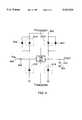
FIG. 9 is a schematic diagram of an alternate embodiment of a parasitic-capacitance-compensated T/H circuit 900 constructed in accordance with the principles of the present invention.
Referring to FIG. 9,MOS transistors Capacitor 904 is coupled to the drains ofMOS transistors Resistor 906 represents the input source impedance of T/H circuit 900. Parasitic junction capacitances ofMOS transistors PJC diodes PJC diodes MOS transistors
As can be seen from FIG. 9, two complementary pairs of PJC diodes (911 and 912, 913 and 914) are present in T/H circuit 900 that, in accordance with the principles of the present invention, have offsetting effects. Depending on the geometries selected for the junctions ofMOS transistors CJC diodes 922 may, for example, be added as needed: (1) between the source ofMOS transistor 902 andbias voltage node 920; (2) between the drain ofMOS transistor 902 andbias voltage node 920; or (3) oneCJC diode 922 each between the source and drain ofMOS transistor 902 andbias voltage node 920. The anode of afirst CJC diode 922 may be coupled to the source ofMOS transistor 902, and the cathode offirst CJC diode 922 tobias voltage node 920. Likewise, the anode of asecond CJC diode 922 may be coupled to the drain ofMOS transistor 902, and the cathode ofsecond CJC diode 922 tobias voltage node 920. Alternatively, either or both of first andsecond CJC diodes 922 may be coupled between ground and the drain or source of MOS transistor 901 (not shown on FIG. 9). Thus, the parasitic junction capacitances of the circuit may be linearized to improve harmonic distortion atoutput node 910. And, this linearization of parasitic-junction capacitances is not limited to manufacturing processes which permit access to the substrate or other anode of the transistor-junctions.
In operation, an input signal VIN causes the voltage atinput node 908 to vary. When the gate ofMOS transistor 902 is coupled to a voltage greater than the voltage atinput node 908, and the gate ofMOS transistor 901 is coupled to a voltage lower than the voltage atinput node 908, the switch comprised ofMOS transistors capacitor 904 to charge and discharge so that the output VOUT atoutput node 910 follows the input signal VIN (i.e., tracking mode). When the gate of theMOS transistor 902 is coupled to a voltage less than the voltage atinput node 908 or the gate of theMOS transistor 901 is coupled to a voltage greater than the voltage atinput node 908, the switch comprised ofMOS transistors capacitor 904 andoutput node 910 so that output VOUT atoutput node 910 remains constant (i.e., hold mode). Thus, signals VTRIGGER1 and VTRIGGER2 at the gates ofMOS transistors
When the switch comprised ofMOS transistors input node 908 changes the voltage acrossPJC diodes PJC diodes PJC diodes PJC diodes CJC diodes 922 added to T/H circuit 900 varies. The parasitic junction capacitances represented byPJC diodes PJC diodes CJC diodes 922, as needed, the net parasitic junction capacitances can be further linearized.
It will be apparent to persons of ordinary skill in the art that, although the present invention has been discussed above with reference to FIGS. 6-9, wherein the T/H circuit transistor comprises a MOSFET transistor, the present invention is applicable to other circuit configurations and types of input devices as well. For example, a JFET may be employed instead of a MOSFET. It will be further apparent that either p-channel or n-channel MOSFETs or JFETs may be used.
In addition, persons skilled in the art will recognize that methods other than the discussed implantation or diffusion may be employed in manufacturing integrated circuits that may take advantage of the principles of the resent invention.
Persons skilled in the art will also appreciate that other circuits exist or providing a track and hold circuit, and that such circuits will likewise benefit from compensation of the parasitic junction capacitances in accordance with the principles of the present invention.
Additionally, although the present invention has been discussed above with reference to a track and hold circuit, other uses exist for compensation of parasitic junction capacitances in accordance with the principles of the present invention.
Persons skilled in the art will thus appreciate that the present invention can be practiced by other than the described embodiments, which are presented for purposes of illustration and not of limitation, and thus the present invention is limited only by the claims which follow.
Claims (17)
1. A method of linearizing parasitic junction capacitances in a circuit employing a transistor having drain, gate and source terminals, said method comprising the steps of:
providing a bias voltage to the circuit at a bias voltage terminal;
inserting a first diode between the source terminal of the transistor and the bias voltage terminal; and
inserting a second diode between the drain terminal of the transistor and the bias voltage terminal.
2. A method of linearizing parasitic junction capacitances in an integrated circuit track and hold circuit, employing a transistor having drain, gate and source terminals, said method comprising the steps of:
receiving a voltage varying input at the source terminal of the transistor;
receiving a trigger input at the gate terminal of the transistor;
compensating for parasitic junction capacitances of the transistor by providing a bias voltage at a bias voltage terminal, adding a first diode between the source terminal of the transistor and the bias voltage terminal, and adding a second diode between the drain terminal of the transistor and the bias voltage terminal;
providing an output at the drain terminal of the transistor.
3. A parisitic-junction-capacitance-compensated circuit comprising:
a bias voltage terminal;
a transistor having source, drain and gate terminals;
a first diode, coupled between the drain terminal and the bias voltage terminal, that compensates for parasitic junction capacitance of the drain terminal; and
a second diode, coupled between the source terminal and the bias voltage terminal, that compensates for parasitic junction capacitance of the source terminal.
4. A parasitic-junction-capacitance-compensated track and hold circuit having an input and an output and a trigger, said track and hold circuit comprising:
a bias voltage terminal;
a transistor having source, drain and gate terminals;
a capacitor coupled between the drain terminal and ground;
a first diode, coupled between the drain terminal and the bias voltage terminal, that compensates parasitic junction capacitance of the drain terminal; and
a second diode, coupled between the source terminal and the bias voltage terminal, that compensates for parasitic junction capacitance of the source terminal;
wherein a voltage varying input signal is received at the input, and upon the trigger, alternatively outputting: (1) a varying signal substantially equal to the input signal; or (2) a constant signal substantially equal to the value of the input signal when the trigger was received.
5. The track and hold circuit of claim 4, wherein the bias voltage terminal, the transistor, the capacitor and the first and second diodes comprise a single integrated circuit.
6. The track and hold circuit of claim 4, wherein the transistor is an n-type transistor.
7. The track and hold circuit of claim 4, wherein the transistor is a p-type transistor.
8. A parasitic-junction-capacitance-compensated track and hold circuit comprising:
a bias voltage node;
a transistor having a source, a drain and a gate;
a capacitor coupled between the drain and ground;
a first diode, coupled between the drain and the bias voltage node, that compensates for parasitic junction capacitance of the drain; and
a second diode, coupled between the source and the bias voltage node, that compensates for parasitic junction capacitance of the source;
wherein a voltage varying input signal is received at the source and a trigger signal is received at the gate to alternatively provide as output at the drain: (1) the voltage varying input signal, or (2) a constant signal of voltage substantially equal to the input signal upon receipt of the trigger signal.
9. The track and hold circuit of claim 8, wherein the bias voltage node, the transistor, the capacitor and the first and second diodes comprise a single integrated circuit.
10. The track and hold circuit of claim 8, wherein the transistor is an n-type transistor.
11. The track and hold circuit of claim 8, wherein the transistor is a p-type transistor.
12. A parasitic-junction-capacitance-compensated track and hold circuit comprising:
first and second transistors of complementary types, each transistor having a source, a drain and a gate, and there being parasitic junction capacitance associated with the source-gate and drain-gate junctions, the first and second transistors having commonly coupled sources and commonly coupled drains;
a capacitor coupled between ground and the drains of the first and second transistor;
wherein a voltage varying input signal is received at the sources of the first and second transistors and a trigger signal is received at the gates of the first and second transistors to alternatively provide as output at the drain: (1) the voltage-varying input signal, or (2) a constant signal of voltage substantially equal to the input signal upon receipt of the trigger signal; and
wherein the parasitic capacitances of the source-gate and drain-gate junctions of the second transistor linearize the parasitic capacitances of the source-gate and drain-gate junctions of the first transistor.
13. The track and hold circuit of claim 12, wherein the first and second transistors and the capacitor comprise a single integrated circuit.
14. The track and hold circuit of claim 13, further comprising:
a bias voltage terminal;
a first diode, coupled between the drain of the first transistor and the bias voltage terminal, that compensates for parasitic junction capacitances of the drain of the first transistor; and
a second diode, coupled between the source of the first transistor and the bias voltage terminal, that compensates for parasitic junction capacitance of the source of the first transistor.
15. The track and hold circuit of claim 14, wherein the first and second diodes further comprise the single integrated circuit.
16. The track and hold circuit of claim 13, further comprising:
a bias voltage terminal;
a first diode, coupled between the drain of the first transistor and the bias voltage terminal, that compensates for parasitic junction capacitances of the drain of the second transistor; and
a second diode, coupled between the source of the first transistor and the bias voltage terminal, that compensates for parasitic junction capacitance of the source of the second transistor.
17. The track and hold circuit of claim 16, wherein the first and second diodes further comprise the single integrated circuit.
Priority Applications (2)
| Application Number | Priority Date | Filing Date | Title |
|---|---|---|---|
| US08/647,361US5763924A (en) | 1996-05-09 | 1996-05-09 | Circuits and methods for compensating non-linear capacitances to minimize harmonic distortion |
| IE970334AIE80408B1 (en) | 1996-05-09 | 1997-05-08 | Circuits and methods for compensating non-linear capacitances to minimize harmonic distortion |
Applications Claiming Priority (1)
| Application Number | Priority Date | Filing Date | Title |
|---|---|---|---|
| US08/647,361US5763924A (en) | 1996-05-09 | 1996-05-09 | Circuits and methods for compensating non-linear capacitances to minimize harmonic distortion |
Publications (1)
| Publication Number | Publication Date |
|---|---|
| US5763924Atrue US5763924A (en) | 1998-06-09 |
Family
ID=24596684
Family Applications (1)
| Application Number | Title | Priority Date | Filing Date |
|---|---|---|---|
| US08/647,361Expired - LifetimeUS5763924A (en) | 1996-05-09 | 1996-05-09 | Circuits and methods for compensating non-linear capacitances to minimize harmonic distortion |
Country Status (2)
| Country | Link |
|---|---|
| US (1) | US5763924A (en) |
| IE (1) | IE80408B1 (en) |
Cited By (23)
| Publication number | Priority date | Publication date | Assignee | Title |
|---|---|---|---|---|
| US20080111714A1 (en)* | 2006-11-14 | 2008-05-15 | Viktor Kremin | Capacitance to code converter with sigma-delta modulator |
| US20080136792A1 (en)* | 2006-12-07 | 2008-06-12 | Tao Peng | Preventing unintentional activation of a touch-sensor button caused by a presence of conductive liquid on the touch-sensor button |
| US20080196945A1 (en)* | 2007-02-21 | 2008-08-21 | Jason Konstas | Preventing unintentional activation of a sensor element of a sensing device |
| US8058937B2 (en) | 2007-01-30 | 2011-11-15 | Cypress Semiconductor Corporation | Setting a discharge rate and a charge rate of a relaxation oscillator circuit |
| US8089289B1 (en) | 2007-07-03 | 2012-01-03 | Cypress Semiconductor Corporation | Capacitive field sensor with sigma-delta modulator |
| US8089288B1 (en) | 2006-11-16 | 2012-01-03 | Cypress Semiconductor Corporation | Charge accumulation capacitance sensor with linear transfer characteristic |
| US8169238B1 (en) | 2007-07-03 | 2012-05-01 | Cypress Semiconductor Corporation | Capacitance to frequency converter |
| US8248084B2 (en) | 2006-03-31 | 2012-08-21 | Cypress Semiconductor Corporation | Touch detection techniques for capacitive touch sense systems |
| US8321174B1 (en) | 2008-09-26 | 2012-11-27 | Cypress Semiconductor Corporation | System and method to measure capacitance of capacitive sensor array |
| US8358142B2 (en) | 2008-02-27 | 2013-01-22 | Cypress Semiconductor Corporation | Methods and circuits for measuring mutual and self capacitance |
| US8487639B1 (en) | 2008-11-21 | 2013-07-16 | Cypress Semiconductor Corporation | Receive demodulator for capacitive sensing |
| US8493351B2 (en) | 2006-03-30 | 2013-07-23 | Cypress Semiconductor Corporation | Apparatus and method for reducing average scan rate to detect a conductive object on a sensing device |
| US8525798B2 (en) | 2008-01-28 | 2013-09-03 | Cypress Semiconductor Corporation | Touch sensing |
| US8564313B1 (en) | 2007-07-03 | 2013-10-22 | Cypress Semiconductor Corporation | Capacitive field sensor with sigma-delta modulator |
| US8570052B1 (en) | 2008-02-27 | 2013-10-29 | Cypress Semiconductor Corporation | Methods and circuits for measuring mutual and self capacitance |
| CN103633948A (en)* | 2013-11-27 | 2014-03-12 | 苏州贝克微电子有限公司 | Circuit for compensating nonlinear capacitance to reduce harmonic distortion to greatest extent |
| US8866500B2 (en) | 2009-03-26 | 2014-10-21 | Cypress Semiconductor Corporation | Multi-functional capacitance sensing circuit with a current conveyor |
| US8976124B1 (en) | 2007-05-07 | 2015-03-10 | Cypress Semiconductor Corporation | Reducing sleep current in a capacitance sensing system |
| US9104273B1 (en) | 2008-02-29 | 2015-08-11 | Cypress Semiconductor Corporation | Multi-touch sensing method |
| US9268441B2 (en) | 2011-04-05 | 2016-02-23 | Parade Technologies, Ltd. | Active integrator for a capacitive sense array |
| US9417728B2 (en) | 2009-07-28 | 2016-08-16 | Parade Technologies, Ltd. | Predictive touch surface scanning |
| US9500686B1 (en) | 2007-06-29 | 2016-11-22 | Cypress Semiconductor Corporation | Capacitance measurement system and methods |
| EP1760887A3 (en)* | 2005-08-18 | 2017-01-04 | Linear Technology Corporation | Circuits and methods for cancelling signal dependent capacitance |
Citations (5)
| Publication number | Priority date | Publication date | Assignee | Title |
|---|---|---|---|---|
| US3836791A (en)* | 1973-07-13 | 1974-09-17 | Us Navy | Presettable single-input voltage-time integrator |
| US4999585A (en)* | 1989-11-06 | 1991-03-12 | Burr-Brown Corporation | Circuit technique for cancelling non-linear capacitor-induced harmonic distortion |
| US5172019A (en)* | 1992-01-17 | 1992-12-15 | Burr-Brown Corporation | Bootstrapped FET sampling switch |
| US5187390A (en)* | 1991-07-12 | 1993-02-16 | Crystal Semiconductor Corporation | Input sampling switch charge conservation |
| US5266820A (en)* | 1990-10-04 | 1993-11-30 | U.S. Philips Corp. | Distributed threshold voltage field effect transistor |
- 1996
- 1996-05-09USUS08/647,361patent/US5763924A/ennot_activeExpired - Lifetime
- 1997
- 1997-05-08IEIE970334Apatent/IE80408B1/ennot_activeIP Right Cessation
Patent Citations (5)
| Publication number | Priority date | Publication date | Assignee | Title |
|---|---|---|---|---|
| US3836791A (en)* | 1973-07-13 | 1974-09-17 | Us Navy | Presettable single-input voltage-time integrator |
| US4999585A (en)* | 1989-11-06 | 1991-03-12 | Burr-Brown Corporation | Circuit technique for cancelling non-linear capacitor-induced harmonic distortion |
| US5266820A (en)* | 1990-10-04 | 1993-11-30 | U.S. Philips Corp. | Distributed threshold voltage field effect transistor |
| US5187390A (en)* | 1991-07-12 | 1993-02-16 | Crystal Semiconductor Corporation | Input sampling switch charge conservation |
| US5172019A (en)* | 1992-01-17 | 1992-12-15 | Burr-Brown Corporation | Bootstrapped FET sampling switch |
Non-Patent Citations (2)
| Title |
|---|
| Hamade, A.R., "Temperature Compensated Quad Analog Switch," IEEE Journal of Solid-State Circuits, vol. SC-14, No. 6, Dec. 19, 1979, pp. 944-952. |
| Hamade, A.R., Temperature Compensated Quad Analog Switch, IEEE Journal of Solid State Circuits, vol. SC 14, No. 6, Dec. 19, 1979, pp. 944 952.* |
Cited By (41)
| Publication number | Priority date | Publication date | Assignee | Title |
|---|---|---|---|---|
| EP1760887A3 (en)* | 2005-08-18 | 2017-01-04 | Linear Technology Corporation | Circuits and methods for cancelling signal dependent capacitance |
| US8493351B2 (en) | 2006-03-30 | 2013-07-23 | Cypress Semiconductor Corporation | Apparatus and method for reducing average scan rate to detect a conductive object on a sensing device |
| US9152284B1 (en) | 2006-03-30 | 2015-10-06 | Cypress Semiconductor Corporation | Apparatus and method for reducing average scan rate to detect a conductive object on a sensing device |
| US9494627B1 (en) | 2006-03-31 | 2016-11-15 | Monterey Research, Llc | Touch detection techniques for capacitive touch sense systems |
| US8248084B2 (en) | 2006-03-31 | 2012-08-21 | Cypress Semiconductor Corporation | Touch detection techniques for capacitive touch sense systems |
| US20080111714A1 (en)* | 2006-11-14 | 2008-05-15 | Viktor Kremin | Capacitance to code converter with sigma-delta modulator |
| US9154160B2 (en) | 2006-11-14 | 2015-10-06 | Cypress Semiconductor Corporation | Capacitance to code converter with sigma-delta modulator |
| US8547114B2 (en) | 2006-11-14 | 2013-10-01 | Cypress Semiconductor Corporation | Capacitance to code converter with sigma-delta modulator |
| US9166621B2 (en) | 2006-11-14 | 2015-10-20 | Cypress Semiconductor Corporation | Capacitance to code converter with sigma-delta modulator |
| US8089288B1 (en) | 2006-11-16 | 2012-01-03 | Cypress Semiconductor Corporation | Charge accumulation capacitance sensor with linear transfer characteristic |
| US8902172B2 (en) | 2006-12-07 | 2014-12-02 | Cypress Semiconductor Corporation | Preventing unintentional activation of a touch-sensor button caused by a presence of conductive liquid on the touch-sensor button |
| US20080136792A1 (en)* | 2006-12-07 | 2008-06-12 | Tao Peng | Preventing unintentional activation of a touch-sensor button caused by a presence of conductive liquid on the touch-sensor button |
| US8058937B2 (en) | 2007-01-30 | 2011-11-15 | Cypress Semiconductor Corporation | Setting a discharge rate and a charge rate of a relaxation oscillator circuit |
| US20080196945A1 (en)* | 2007-02-21 | 2008-08-21 | Jason Konstas | Preventing unintentional activation of a sensor element of a sensing device |
| US8976124B1 (en) | 2007-05-07 | 2015-03-10 | Cypress Semiconductor Corporation | Reducing sleep current in a capacitance sensing system |
| US10788937B2 (en) | 2007-05-07 | 2020-09-29 | Cypress Semiconductor Corporation | Reducing sleep current in a capacitance sensing system |
| US12181943B2 (en) | 2007-05-07 | 2024-12-31 | Cypress Semiconductor Corporation | Reducing sleep current in a capacitance sensing system |
| US9500686B1 (en) | 2007-06-29 | 2016-11-22 | Cypress Semiconductor Corporation | Capacitance measurement system and methods |
| US8169238B1 (en) | 2007-07-03 | 2012-05-01 | Cypress Semiconductor Corporation | Capacitance to frequency converter |
| US8570053B1 (en) | 2007-07-03 | 2013-10-29 | Cypress Semiconductor Corporation | Capacitive field sensor with sigma-delta modulator |
| US8564313B1 (en) | 2007-07-03 | 2013-10-22 | Cypress Semiconductor Corporation | Capacitive field sensor with sigma-delta modulator |
| US8536902B1 (en)* | 2007-07-03 | 2013-09-17 | Cypress Semiconductor Corporation | Capacitance to frequency converter |
| US8089289B1 (en) | 2007-07-03 | 2012-01-03 | Cypress Semiconductor Corporation | Capacitive field sensor with sigma-delta modulator |
| US8525798B2 (en) | 2008-01-28 | 2013-09-03 | Cypress Semiconductor Corporation | Touch sensing |
| US9760192B2 (en) | 2008-01-28 | 2017-09-12 | Cypress Semiconductor Corporation | Touch sensing |
| US9423427B2 (en) | 2008-02-27 | 2016-08-23 | Parade Technologies, Ltd. | Methods and circuits for measuring mutual and self capacitance |
| US8358142B2 (en) | 2008-02-27 | 2013-01-22 | Cypress Semiconductor Corporation | Methods and circuits for measuring mutual and self capacitance |
| US8692563B1 (en) | 2008-02-27 | 2014-04-08 | Cypress Semiconductor Corporation | Methods and circuits for measuring mutual and self capacitance |
| US9494628B1 (en) | 2008-02-27 | 2016-11-15 | Parade Technologies, Ltd. | Methods and circuits for measuring mutual and self capacitance |
| US8570052B1 (en) | 2008-02-27 | 2013-10-29 | Cypress Semiconductor Corporation | Methods and circuits for measuring mutual and self capacitance |
| US9104273B1 (en) | 2008-02-29 | 2015-08-11 | Cypress Semiconductor Corporation | Multi-touch sensing method |
| US8321174B1 (en) | 2008-09-26 | 2012-11-27 | Cypress Semiconductor Corporation | System and method to measure capacitance of capacitive sensor array |
| US11029795B2 (en) | 2008-09-26 | 2021-06-08 | Cypress Semiconductor Corporation | System and method to measure capacitance of capacitive sensor array |
| US10386969B1 (en) | 2008-09-26 | 2019-08-20 | Cypress Semiconductor Corporation | System and method to measure capacitance of capacitive sensor array |
| US8575947B1 (en) | 2008-11-21 | 2013-11-05 | Cypress Semiconductor Corporation | Receive demodulator for capacitive sensing |
| US8487639B1 (en) | 2008-11-21 | 2013-07-16 | Cypress Semiconductor Corporation | Receive demodulator for capacitive sensing |
| US8866500B2 (en) | 2009-03-26 | 2014-10-21 | Cypress Semiconductor Corporation | Multi-functional capacitance sensing circuit with a current conveyor |
| US9442146B2 (en) | 2009-03-26 | 2016-09-13 | Parade Technologies, Ltd. | Multi-mode capacitive sensing device and method with current conveyor |
| US9417728B2 (en) | 2009-07-28 | 2016-08-16 | Parade Technologies, Ltd. | Predictive touch surface scanning |
| US9268441B2 (en) | 2011-04-05 | 2016-02-23 | Parade Technologies, Ltd. | Active integrator for a capacitive sense array |
| CN103633948A (en)* | 2013-11-27 | 2014-03-12 | 苏州贝克微电子有限公司 | Circuit for compensating nonlinear capacitance to reduce harmonic distortion to greatest extent |
Also Published As
| Publication number | Publication date |
|---|---|
| IE80408B1 (en) | 1998-06-17 |
| IE970334A1 (en) | 1997-11-19 |
Similar Documents
| Publication | Publication Date | Title |
|---|---|---|
| US5763924A (en) | Circuits and methods for compensating non-linear capacitances to minimize harmonic distortion | |
| US6885234B2 (en) | Resistance load source follower circuit | |
| US5095284A (en) | Subthreshold CMOS amplifier with wide input voltage range | |
| USRE42494E1 (en) | Preventing drain to body forward bias in a MOS transistor | |
| US4843265A (en) | Temperature compensated monolithic delay circuit | |
| US4435652A (en) | Threshold voltage control network for integrated circuit field-effect trransistors | |
| US6275094B1 (en) | CMOS device and circuit and method of operation dynamically controlling threshold voltage | |
| US5422583A (en) | Back gate switched sample and hold circuit | |
| WO2001069681A9 (en) | Cascode circuits in duel threshold voltage, bicmos and dtmos technologies | |
| US4736117A (en) | VDS clamp for limiting impact ionization in high density CMOS devices | |
| US5721513A (en) | Gain controlled amplification circuit having differential amplifier | |
| US3956708A (en) | MOSFET comparator | |
| JPH0629762A (en) | High-sensitivity low-noise transistor amplifier | |
| US5801523A (en) | Circuit and method of providing a constant current | |
| US5973544A (en) | Intermediate potential generation circuit | |
| US6462587B2 (en) | Integrated circuit having a comparator circuit including at least one differential amplifier | |
| US4460874A (en) | Three-terminal operational amplifier/comparator with offset compensation | |
| US6084440A (en) | Circuits and methods for canceling harmonic distortion in sample and hold circuits | |
| US4602207A (en) | Temperature and power supply stable current source | |
| KR970005825B1 (en) | Differential current source circuit | |
| US4810903A (en) | BICMOS driver circuit including submicron on chip voltage source | |
| US6133780A (en) | Digitally tunable voltage reference using a neuron MOSFET | |
| US4940910A (en) | Temperature compensated monolithic delay circuit | |
| US6445322B2 (en) | Digital-to-analog converter with improved output impedance switch | |
| US6563447B1 (en) | Non-linear bulk capacitance bootstrapped current switch |
Legal Events
| Date | Code | Title | Description |
|---|---|---|---|
| AS | Assignment | Owner name:LINEAR TECHNOLOGY CORPORATION, CALIFORNIA Free format text:ASSIGNMENT OF ASSIGNORS INTEREST;ASSIGNORS:LUM, SAMMY S.;REMPFER, WILLIAM C.;REEL/FRAME:008465/0541 Effective date:19960708 | |
| STCF | Information on status: patent grant | Free format text:PATENTED CASE | |
| FPAY | Fee payment | Year of fee payment:4 | |
| FPAY | Fee payment | Year of fee payment:8 | |
| FEPP | Fee payment procedure | Free format text:PAYOR NUMBER ASSIGNED (ORIGINAL EVENT CODE: ASPN); ENTITY STATUS OF PATENT OWNER: LARGE ENTITY | |
| FPAY | Fee payment | Year of fee payment:12 | |
| AS | Assignment | Owner name:ANALOG DEVICES INTERNATIONAL UNLIMITED COMPANY, IRELAND Free format text:CHANGE OF NAME;ASSIGNOR:LINEAR TECHNOLOGY LLC;REEL/FRAME:057423/0429 Effective date:20181105 Owner name:LINEAR TECHNOLOGY LLC, CALIFORNIA Free format text:CHANGE OF NAME;ASSIGNOR:LINEAR TECHNOLOGY CORPORATION;REEL/FRAME:057421/0355 Effective date:20170502 |