US5763307A - Block select transistor and method of fabrication - Google Patents
Block select transistor and method of fabricationDownload PDFInfo
- Publication number
- US5763307A US5763307AUS08/745,278US74527896AUS5763307AUS 5763307 AUS5763307 AUS 5763307AUS 74527896 AUS74527896 AUS 74527896AUS 5763307 AUS5763307 AUS 5763307A
- Authority
- US
- United States
- Prior art keywords
- layer
- forming
- depositing
- metal
- substrate
- Prior art date
- Legal status (The legal status is an assumption and is not a legal conclusion. Google has not performed a legal analysis and makes no representation as to the accuracy of the status listed.)
- Expired - Lifetime
Links
Images


Classifications
- H—ELECTRICITY
- H10—SEMICONDUCTOR DEVICES; ELECTRIC SOLID-STATE DEVICES NOT OTHERWISE PROVIDED FOR
- H10B—ELECTRONIC MEMORY DEVICES
- H10B41/00—Electrically erasable-and-programmable ROM [EEPROM] devices comprising floating gates
- H10B41/40—Electrically erasable-and-programmable ROM [EEPROM] devices comprising floating gates characterised by the peripheral circuit region
- H10B41/42—Simultaneous manufacture of periphery and memory cells
- H10B41/43—Simultaneous manufacture of periphery and memory cells comprising only one type of peripheral transistor
- H—ELECTRICITY
- H10—SEMICONDUCTOR DEVICES; ELECTRIC SOLID-STATE DEVICES NOT OTHERWISE PROVIDED FOR
- H10B—ELECTRONIC MEMORY DEVICES
- H10B69/00—Erasable-and-programmable ROM [EPROM] devices not provided for in groups H10B41/00 - H10B63/00, e.g. ultraviolet erasable-and-programmable ROM [UVEPROM] devices
Definitions
- the present inventionrelates to flash memory devices, and more particularly to a flash memory structure having a reduced physical area by having a modified core array layout containing both a block select transistor array and a core memory array.
- Flash memory devicesare becoming increasingly popular in data storage applications.
- flashelectrically erasable and programmable read-only memory or “Flash EEPROMs” generally refer to EEPROM memory cells which are programmed by hot electron injection and erased by Fowler-Nordheim tunneling.
- an array of flash EEPROM memory cellsmay be formed on a semiconductor substrate in a series of rows and columns, accessed by wordlines and bitlines.
- the wordlinesare connected to the control gate of each flash EEPROM memory cell in a given row.
- the bitlinesare coupled to the drain of each individual EEPROM memory cell along a given column.
- the memory cellsare arranged in a common region, with the memory cell region of the flash memory array being referred to as the "core" area of the chip. All other components necessary for the operation of the flash memory devices, such as block select transistors, charge pumps, etc. are located in the peripheral area of the chip.
- the peripheral area of a flash memorycontains devices of varying sizes and are generally formed on a section of the chip different from the core array. More specifically, in standard flash EEPROM devices the memory array is defined by a particular number of sectors. Each sector includes a core array portion and a peripheral portion. For example, if a flash EEPROM device contains six sectors, each of those sectors contains a core array having a given number of transistors and a separate peripheral array, fabricated outside the core array, which contains the block select transistors used to select which of the core array transistors is going to be operated upon. In conventional flash EEPROM devices, a non-volatile random access memory (RAM) chip is used as a select transistor.
- RAMnon-volatile random access memory
- Standard flash EEPROM structurestake up a large amount of die space. With the industry trend of providing more and more memory capacity on a given integrated circuit chip, physical area becomes a premium. The standard fabrication and layout techniques are insufficient to handle the limited space requirements required by the present trend of reducing component sizes.
- a flash EEPROM memory devicehaving a core array formed on a semiconductor substrate, the core array containing a plurality of transistors operable to store data; a peripheral array formed on a semiconductor substrate, with the peripheral array being fabricated within the core array and further including a plurality of transistors operable to select from among the core array transistors; and a ground plate fabricated between the core array and the peripheral array, wherein the core array and the peripheral array are fabricated on the same portion of the integrated circuit chip.
- the layout of the flash EEPROM deviceplaces the peripheral components of the device into the core array thereby reducing the total area taken up by the memory array.
- a ground plateis used to isolate the areas where high voltage components should not be located. With the use of the ground plate, higher voltage peripheral components can be placed within the core array.
- An advantage of the present inventionis the ability to increase flash memory density by fabricating a flash memory device on a reduced die space.
- Another advantage of the present inventionis that it reduces fabrication costs.
- a feature of the present inventionis that it can be performed with standard processing techniques.
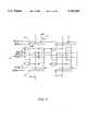
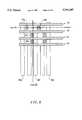
- FIG. 1depicts a top view of the block select sector of a standard flash EEPROM device.
- FIG. 2represents a schematic diagram of a flash memory device having a layout according to the present invention.
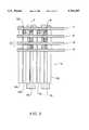
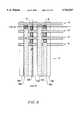
- FIG. 3provides a top view of the flash EEPROM device having a reduced physical area fabricated according to the present invention.
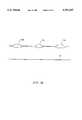
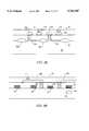
- FIGS. 4-4Ashows the top view and view along line AA of the flash EEPROM cell layout according to the present invention.
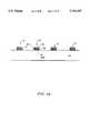
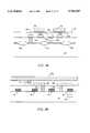
- FIGS. 5-5Adepict a top view and a view along line BB of a ground plate structure fabricated according to the present invention.
- FIG. 6shows a top view of the block select transistor fabrication according to the present invention.
- FIGS. 6A-6Bshows a view along lines AA and BB, respectively, of the block select transistor section fabricated according to the present invention.
- FIG. 7is a top view of the fabrication of the block select sector and bitlines of the core memory array according to the present invention.
- FIGS. 7A-7Bprovide views of the block select section and bitline layout according to the present invention along lines AA and BB, respectively.
- FIG. 8provides a top view of the further fabrication of the block select section of the core array according to the present invention.
- FIGS. 8A-8Bprovide a view of the block select section of the core array according to the present invention along lines AA and BB, respectively.
- FIG. 9-9Billustrates the final structure of the block select transistor section according to the present invention.
- FIG. 1depicts a portion of a standard flash memory cell. As shown in FIG. 1, the area taken up by the peripheral devices 2 and the interface devices 3, for coupling the flash EEPROM device with external devices, takes up a large amount of the overall memory area. As discussed above, the varying sizes of the peripheral devices 2 is what requires the most space for a given device area.
- FIG. 2shows a partial schematic top view of the flash EEPROM device layout according to the present invention.
- FIG. 2presents a single sector fabricated along sector select line M2 15. This sector contains two rows of transistors along wordlines WLmm and WLm+1n, respectively.
- Select line 20is used to select a first set of core array transistors and is shown at the top of FIG. 2.
- Select line 22is used to select a subsequent series of core array transistors and is presented at the bottom of FIG. 2.
- the flash EEPROM memory deviceincludes 20 0.8 ⁇ n-channel select transistors. Each transistor selects a particular sector within the core memory array 12. There are 512 wordlines in each sector. Each sector has 8 input/output (I/O) blocks, with each I/O block having 128 columns of memory cells. Also present in the flash EEPROM memory device of the present invention are two redundant elements, each having four columns of cells. Thus, in each sector of the flash EEPROM memory device, there are a total of 1,032 columns. For ease of description, and for obtaining a thorough understanding of the present invention, only two sectors of the flash EEPROM device of the present invention will be discussed.
- FIG. 3shows the flash EEPROM memory block sector layout according to the present invention.
- Select transistors 20 and 22, respectivelyare contained within the core array 10 of a flash EEPROM memory device.
- the block select transistors 20 and 22are separated from the core array transistors 12 by ground plates 14 and 16, respectively.
- the block select transistors 20 and 22are used to select among a plurality of core array transistors 12.
- the sector of memory shown in FIG. 3can be coupled to external elements through jumpers 17 and 18, respectively, which are fabricated along metal II lines 15a and 15b, respectively.
- FIG. 1A view of FIG. 1 in relation to FIG. 3, shows the reduced area provided by the layout of the present invention.
- the peripheral array 4 and the interface circuitry 3(FIG. 1), which take a large amount of die area in a standard EEPROM architecture, can be placed within the much smaller area denoted A, of the core array according to the layout and fabrication steps of the present invention.
- Athe much smaller area denoted A, of the core array according to the layout and fabrication steps of the present invention.
- FIGS. 2 and 3The fabrication process for providing the flash EEPROM device structure as depicted in FIGS. 2 and 3 will be presented with respect to FIGS. 4-9.
- the fabrication process of the present inventionstarts with a semiconductor substrate 50 (FIG. 4) having formed thereon oxide isolation regions 30A-30E for providing device isolation between the core array transistors to be subsequently formed.
- the oxide isolation regions 30A-30Eare formed using standard local oxidation of silicon (LOCOS) techniques.
- FIG. 4Ashows a cross-sectional view of the initial processing steps of the present invention where isolation regions 30A, 30C and 30E are formed on the semiconductor substrate 50.
- the groundplates 14 and 16, respectively, and the select transistors 20 and 22are provided on the semiconductor substrate 50.
- the purpose of the groundplateis to isolate the high voltage elements, such that the cross-talk between the high voltage elements and the core array cells will be minimized.
- the groundplate 14(FIG. 5A) is fabricated by growing a thin tunnel oxide layer 46 having a thickness of approximately 100 ⁇ over the semiconductor substrate 50. Next, a polysilicon layer 41 is grown on top of the thin oxide layer 46. A ground voltage is applied to the polysilicon layer 41 thereby insuring that the voltage on either side of the oxide layer will not communicate with one another.
- the select transistors 20 and 22are fabricated by providing a polyI layer 40 on top of the tunnel oxide.
- a polyII layer 42is deposited on top of the entire length of the polyI layer 40.
- a tungsten silicide layer 44is applied on top of the polyI and polyII layers 40 and 42, respectively forming a base structure.
- the base structureis then masked (not shown) and is subsequently etched by a reaction ion etch (RIE) method to provide the structure as shown in FIG. 5A.
- RIEreaction ion etch
- PolyI and polyII layers 41 and 42, respectivelyare contiguous and function like a single polyI layer.
- the polyI layer 40 and the polyII layer 42experience a good electrical connection because the polyI and polyII layers 40 and 42, respectively, are connected along their entire length.
- FIGS. 6 and 6Ashow the next processing step where an interlayer dielectric (ILD)60 is applied on top of the transistor structure shown in FIG. 5A.
- the interlayer dielectric 60is generally comprised of conventional isolation reflow glass.
- Tungsten contact plugs 52A and 52B, respectively,are applied to the block select transistor structure by first boring a hole in the interlayer dielectric 60 using standard processing techniques then refilling these holes with tungsten material.
- the tungsten contact plugs 52A and 52Bare used to provide a contact between the select transistors 20 and 22 to the metal bitlines 62A-62D that are fabricated in the next processing step as shown in FIG. 7.
- bitlines rows M1, 62A-62Dare provided as shown in FIG. 7.
- FIGS. 7A and 7Bshow that the deposited metal1 lines 62A-62D provide four bitlines for communication with the columns of core transistors 12 contained in the two sectors described herein.
- FIG. 7Bshows how the metal1 bitline 62B is connected to select transistors 20 and 22, respectively.
- the jumper 17 for connecting the bitlines 62A-62D to the select lines (to be fabricated subsequently)is provided on top of the metal1 bitlines M1 by first providing a hole in ILD layer 60 then filling the hole with a jumper material. As discussed above, the jumper 17 is used to provide a contact between the metal1 52A bitline and the sector select lines (not shown), through the interlayer dielectric 60. In the final processing step, the metal2 lines 15A and 15B are deposited over the interlayer dielectric layer 60 and contact jumper 17 respectively.
- the metal2 line 15A-15Bhas a width of 2L, where L is the minimum design rule of the memory cell.
- Lis the minimum design rule of the memory cell.
- the channel width of the core transistorsis one micron (1 82 m) long; or the length of the transistor polysilicon structure is one micron (1 ⁇ m) long.
- the oxide isolation region requiredis two microns (2 ⁇ m). The two micron field isolation region will prevent cross-talk between adjacent devices will not communicate with one another.
- a selection signalis provided along M2 15A which passes through the jumper 17 and transferred to bitline M1 62A-62D.
- the selection signalis then transferred to the wordlines of the core transistors of the flash memory device.
- each M2 lines 15A and 15Bcommunicate with two sublines M1 comprised of the bitlines M1 62A and 62B, respectively. Consequently, two sectors of the flash EEPROM device 10 of the present invention can be controlled by one M2 line 15A.
- the space savings provided by the layout of the present inventionare dependent upon the number of sections used by a particular architecture. Depending upon the number of sections used by a particular architecture, the space savings will vary. For example, if each sector of a particular device architecture contains 16 bits, then the die savings would be 50%. Accordingly, the larger the sector required by a given component architecture, the larger the die space savings will be.
Landscapes
- Engineering & Computer Science (AREA)
- Manufacturing & Machinery (AREA)
- Non-Volatile Memory (AREA)
- Semiconductor Memories (AREA)
Abstract
Description
Claims (17)
Priority Applications (1)
| Application Number | Priority Date | Filing Date | Title |
|---|---|---|---|
| US08/745,278US5763307A (en) | 1996-11-08 | 1996-11-08 | Block select transistor and method of fabrication |
Applications Claiming Priority (1)
| Application Number | Priority Date | Filing Date | Title |
|---|---|---|---|
| US08/745,278US5763307A (en) | 1996-11-08 | 1996-11-08 | Block select transistor and method of fabrication |
Publications (1)
| Publication Number | Publication Date |
|---|---|
| US5763307Atrue US5763307A (en) | 1998-06-09 |
Family
ID=24996017
Family Applications (1)
| Application Number | Title | Priority Date | Filing Date |
|---|---|---|---|
| US08/745,278Expired - LifetimeUS5763307A (en) | 1996-11-08 | 1996-11-08 | Block select transistor and method of fabrication |
Country Status (1)
| Country | Link |
|---|---|
| US (1) | US5763307A (en) |
Cited By (20)
| Publication number | Priority date | Publication date | Assignee | Title |
|---|---|---|---|---|
| US20040165554A1 (en)* | 2002-04-05 | 2004-08-26 | Interdigital Technology Corporation | System for efficient recovery of node B buffered data following serving high speed downlink shared channel cell change |
| US20050157996A1 (en)* | 2001-08-14 | 2005-07-21 | Mccarthy Wil | Fiber incorporating quantum dots as programmable dopants |
| US20070194297A1 (en)* | 2006-02-17 | 2007-08-23 | The Programmable Matter Corporation | Quantum Dot Switching Device |
| US20080061222A1 (en)* | 2006-09-12 | 2008-03-13 | The Programmable Matter Corporation | Electromagnetic sensor incorporating quantum confinement structures |
| US20080204383A1 (en)* | 2007-02-28 | 2008-08-28 | Ravenbrick, Llc | Multicolor Light Emitting Device Incorporating Tunable Quantum Confinement Devices |
| US20090059406A1 (en)* | 2007-03-02 | 2009-03-05 | Ravenbrick, Llc | Wavelength-specific optical switch |
| US20090128893A1 (en)* | 2007-09-19 | 2009-05-21 | Ravenbrick, Llc | Low-emissivity window films and coatings incorporating nanoscale wire grids |
| US20090268273A1 (en)* | 2008-04-23 | 2009-10-29 | Ravenbrick Llc | Glare Management of Reflective and Thermoreflective Surfaces |
| US7659538B2 (en) | 2004-06-04 | 2010-02-09 | Ravenbrick, Llc | Layered composite film incorporating a quantum dot shift register |
| US20100045924A1 (en)* | 2008-08-20 | 2010-02-25 | Ravenbrick, Llc | Methods for Fabricating Thermochromic Filters |
| US20100232017A1 (en)* | 2008-06-19 | 2010-09-16 | Ravenbrick Llc | Optical metapolarizer device |
| US20110025934A1 (en)* | 2009-04-10 | 2011-02-03 | Ravenbrick Llc | Thermally switched optical filter incorporating a refractive optical structure |
| US20110102878A1 (en)* | 2009-10-30 | 2011-05-05 | Ravenbrick Llc | Thermochromic Filters and Stopband Filters for Use with Same |
| US20110234944A1 (en)* | 2010-03-29 | 2011-09-29 | Ravenbrick Llc | Polymer-stabilized thermotropic liquid crystal device |
| US8593581B2 (en) | 2007-01-24 | 2013-11-26 | Ravenbrick Llc | Thermally switched optical downconverting filter |
| US8699114B2 (en) | 2010-06-01 | 2014-04-15 | Ravenbrick Llc | Multifunctional building component |
| US8755105B2 (en) | 2007-07-11 | 2014-06-17 | Ravenbrick Llc | Thermally switched reflective optical shutter |
| US8760750B2 (en) | 2007-12-20 | 2014-06-24 | Ravenbrick Llc | Thermally switched absorptive window shutter |
| US8947760B2 (en) | 2009-04-23 | 2015-02-03 | Ravenbrick Llc | Thermotropic optical shutter incorporating coatable polarizers |
| US10247936B2 (en) | 2009-04-10 | 2019-04-02 | Ravenbrick Llc | Thermally switched optical filter incorporating a guest-host architecture |
Citations (4)
| Publication number | Priority date | Publication date | Assignee | Title |
|---|---|---|---|---|
| US4962058A (en)* | 1989-04-14 | 1990-10-09 | International Business Machines Corporation | Process for fabricating multi-level integrated circuit wiring structure from a single metal deposit |
| US5010028A (en)* | 1989-12-29 | 1991-04-23 | Texas Instruments Incorporated | Method of making hot electron programmable, tunnel electron erasable contactless EEPROM |
| US5597750A (en)* | 1993-07-29 | 1997-01-28 | Sgs-Thomson Microelectronics S.R.L. | Method of manufacturing a matrix of memory cells having control gates |
| US5607873A (en)* | 1996-04-24 | 1997-03-04 | National Semiconductor Corporation | Method for forming contact openings in a multi-layer structure that reduces overetching of the top conductive structure |
- 1996
- 1996-11-08USUS08/745,278patent/US5763307A/ennot_activeExpired - Lifetime
Patent Citations (4)
| Publication number | Priority date | Publication date | Assignee | Title |
|---|---|---|---|---|
| US4962058A (en)* | 1989-04-14 | 1990-10-09 | International Business Machines Corporation | Process for fabricating multi-level integrated circuit wiring structure from a single metal deposit |
| US5010028A (en)* | 1989-12-29 | 1991-04-23 | Texas Instruments Incorporated | Method of making hot electron programmable, tunnel electron erasable contactless EEPROM |
| US5597750A (en)* | 1993-07-29 | 1997-01-28 | Sgs-Thomson Microelectronics S.R.L. | Method of manufacturing a matrix of memory cells having control gates |
| US5607873A (en)* | 1996-04-24 | 1997-03-04 | National Semiconductor Corporation | Method for forming contact openings in a multi-layer structure that reduces overetching of the top conductive structure |
Cited By (39)
| Publication number | Priority date | Publication date | Assignee | Title |
|---|---|---|---|---|
| US20050157996A1 (en)* | 2001-08-14 | 2005-07-21 | Mccarthy Wil | Fiber incorporating quantum dots as programmable dopants |
| US20050157997A1 (en)* | 2001-08-14 | 2005-07-21 | Mccarthy Wil | Fiber incorporating quantum dots as programmable dopants |
| US7276432B2 (en)* | 2001-08-14 | 2007-10-02 | The Programmable Matter Corporation | Fiber incorporating quantum dots as programmable dopants |
| US7655942B2 (en)* | 2001-08-14 | 2010-02-02 | Ravenbrick Llc | Fiber incorporating quantum dots as programmable dopants |
| US20040165554A1 (en)* | 2002-04-05 | 2004-08-26 | Interdigital Technology Corporation | System for efficient recovery of node B buffered data following serving high speed downlink shared channel cell change |
| US7692180B2 (en) | 2004-06-04 | 2010-04-06 | Ravenbrick Llc | Layered composite film incorporating quantum dots as programmable dopants |
| US7659538B2 (en) | 2004-06-04 | 2010-02-09 | Ravenbrick, Llc | Layered composite film incorporating a quantum dot shift register |
| US20070194297A1 (en)* | 2006-02-17 | 2007-08-23 | The Programmable Matter Corporation | Quantum Dot Switching Device |
| US7601946B2 (en) | 2006-09-12 | 2009-10-13 | Ravenbrick, Llc | Electromagnetic sensor incorporating quantum confinement structures |
| US7977621B2 (en) | 2006-09-12 | 2011-07-12 | Ravenbrick Llc | Thermochromic optical filter in which transition wavelength is variable and controllable by adjustable temperature of a chosen quantum well layer |
| US20100027099A1 (en)* | 2006-09-12 | 2010-02-04 | Ravenbrick Llc | Thermochromic Optical Filter Incorporating Quantum Confinement Devices |
| US20080061222A1 (en)* | 2006-09-12 | 2008-03-13 | The Programmable Matter Corporation | Electromagnetic sensor incorporating quantum confinement structures |
| US8593581B2 (en) | 2007-01-24 | 2013-11-26 | Ravenbrick Llc | Thermally switched optical downconverting filter |
| US8363307B2 (en) | 2007-02-28 | 2013-01-29 | Ravenbrick, Llc | Multicolor light emitting device incorporating tunable quantum confinement devices |
| US20080204383A1 (en)* | 2007-02-28 | 2008-08-28 | Ravenbrick, Llc | Multicolor Light Emitting Device Incorporating Tunable Quantum Confinement Devices |
| US7936500B2 (en) | 2007-03-02 | 2011-05-03 | Ravenbrick Llc | Wavelength-specific optical switch |
| US20090059406A1 (en)* | 2007-03-02 | 2009-03-05 | Ravenbrick, Llc | Wavelength-specific optical switch |
| US20110205650A1 (en)* | 2007-03-02 | 2011-08-25 | Ravenbrick Llc | Wavelength-Specific Optical Switch |
| US8755105B2 (en) | 2007-07-11 | 2014-06-17 | Ravenbrick Llc | Thermally switched reflective optical shutter |
| US8908267B2 (en) | 2007-09-19 | 2014-12-09 | Ravenbrick, Llc | Low-emissivity window films and coatings incorporating nanoscale wire grids |
| US20090128893A1 (en)* | 2007-09-19 | 2009-05-21 | Ravenbrick, Llc | Low-emissivity window films and coatings incorporating nanoscale wire grids |
| US8760750B2 (en) | 2007-12-20 | 2014-06-24 | Ravenbrick Llc | Thermally switched absorptive window shutter |
| US8634137B2 (en) | 2008-04-23 | 2014-01-21 | Ravenbrick Llc | Glare management of reflective and thermoreflective surfaces |
| US20090268273A1 (en)* | 2008-04-23 | 2009-10-29 | Ravenbrick Llc | Glare Management of Reflective and Thermoreflective Surfaces |
| US9116302B2 (en) | 2008-06-19 | 2015-08-25 | Ravenbrick Llc | Optical metapolarizer device |
| US20100232017A1 (en)* | 2008-06-19 | 2010-09-16 | Ravenbrick Llc | Optical metapolarizer device |
| US20100045924A1 (en)* | 2008-08-20 | 2010-02-25 | Ravenbrick, Llc | Methods for Fabricating Thermochromic Filters |
| US8665414B2 (en) | 2008-08-20 | 2014-03-04 | Ravenbrick Llc | Methods for fabricating thermochromic filters |
| US9188804B2 (en) | 2008-08-20 | 2015-11-17 | Ravenbrick Llc | Methods for fabricating thermochromic filters |
| US8643795B2 (en) | 2009-04-10 | 2014-02-04 | Ravenbrick Llc | Thermally switched optical filter incorporating a refractive optical structure |
| US20110025934A1 (en)* | 2009-04-10 | 2011-02-03 | Ravenbrick Llc | Thermally switched optical filter incorporating a refractive optical structure |
| US10247936B2 (en) | 2009-04-10 | 2019-04-02 | Ravenbrick Llc | Thermally switched optical filter incorporating a guest-host architecture |
| US8947760B2 (en) | 2009-04-23 | 2015-02-03 | Ravenbrick Llc | Thermotropic optical shutter incorporating coatable polarizers |
| US8867132B2 (en) | 2009-10-30 | 2014-10-21 | Ravenbrick Llc | Thermochromic filters and stopband filters for use with same |
| US20110102878A1 (en)* | 2009-10-30 | 2011-05-05 | Ravenbrick Llc | Thermochromic Filters and Stopband Filters for Use with Same |
| US8828176B2 (en) | 2010-03-29 | 2014-09-09 | Ravenbrick Llc | Polymer stabilized thermotropic liquid crystal device |
| US20110234944A1 (en)* | 2010-03-29 | 2011-09-29 | Ravenbrick Llc | Polymer-stabilized thermotropic liquid crystal device |
| US8699114B2 (en) | 2010-06-01 | 2014-04-15 | Ravenbrick Llc | Multifunctional building component |
| US9256085B2 (en) | 2010-06-01 | 2016-02-09 | Ravenbrick Llc | Multifunctional building component |
Similar Documents
| Publication | Publication Date | Title |
|---|---|---|
| US5763307A (en) | Block select transistor and method of fabrication | |
| US7288455B2 (en) | Method of forming non-volatile memory cell array having discontinuous source and drain diffusions contacted by continuous bit line conductors | |
| US5654917A (en) | Process for making and programming a flash memory array | |
| US6551878B2 (en) | Mini flash process and circuit | |
| JP5072357B2 (en) | Method for making nonvolatile memory cell array | |
| US7202125B2 (en) | Low-voltage, multiple thin-gate oxide and low-resistance gate electrode | |
| US6696724B2 (en) | Two-transistor flash cell | |
| US6420231B1 (en) | Processing techniques for making a dual floating gate EEPROM cell array | |
| US5936274A (en) | High density flash memory | |
| US7416935B2 (en) | Method of manufacturing nonvolatile semiconductor memory device having adjacent selection transistors connected together | |
| US6373095B1 (en) | NVRAM cell having increased coupling ratio between a control gate and floating gate without an increase in cell area | |
| US20090294831A1 (en) | Semiconductor Constructions, Methods Of Forming Transistor Gates, And Methods Of Forming NAND Cell Units | |
| US7052947B2 (en) | Fabrication of gate dielectric in nonvolatile memories in which a memory cell has multiple floating gates | |
| US6939764B2 (en) | Methods of forming memory cells having self-aligned silicide | |
| US20080158965A1 (en) | Operating method of non-volatile memory | |
| US20100327453A1 (en) | Semiconductor Device and Method of Manufacturing the Same | |
| US5397723A (en) | Process for forming arrayed field effect transistors highly integrated on substrate | |
| US7180128B2 (en) | Non-volatile memory, non-volatile memory array and manufacturing method thereof | |
| US20060043368A1 (en) | Flash cell structures and methods of formation | |
| US20060198199A1 (en) | Non-volatile memory and manufacturing method and operating method thereof |
Legal Events
| Date | Code | Title | Description |
|---|---|---|---|
| AS | Assignment | Owner name:ADVANCED MICRO DEVICES, INC., CALIFORNIA Free format text:ASSIGNMENT OF ASSIGNORS INTEREST;ASSIGNORS:WANG, HSINGYA ARTHUR;ZHOU, QIMENG;REEL/FRAME:008304/0208 Effective date:19961107 | |
| STCF | Information on status: patent grant | Free format text:PATENTED CASE | |
| FPAY | Fee payment | Year of fee payment:4 | |
| FEPP | Fee payment procedure | Free format text:PAYOR NUMBER ASSIGNED (ORIGINAL EVENT CODE: ASPN); ENTITY STATUS OF PATENT OWNER: LARGE ENTITY | |
| FPAY | Fee payment | Year of fee payment:8 | |
| AS | Assignment | Owner name:SPANSION INC., CALIFORNIA Free format text:ASSIGNMENT OF ASSIGNORS INTEREST;ASSIGNOR:ADVANCED MICRO DEVICES, INC.;REEL/FRAME:019028/0605 Effective date:20070131 | |
| AS | Assignment | Owner name:SPANSION LLC, CALIFORNIA Free format text:ASSIGNMENT OF ASSIGNORS INTEREST;ASSIGNOR:SPANSION INC.;REEL/FRAME:019063/0777 Effective date:20070131 | |
| FPAY | Fee payment | Year of fee payment:12 | |
| AS | Assignment | Owner name:BARCLAYS BANK PLC,NEW YORK Free format text:SECURITY AGREEMENT;ASSIGNORS:SPANSION LLC;SPANSION INC.;SPANSION TECHNOLOGY INC.;AND OTHERS;REEL/FRAME:024522/0338 Effective date:20100510 Owner name:BARCLAYS BANK PLC, NEW YORK Free format text:SECURITY AGREEMENT;ASSIGNORS:SPANSION LLC;SPANSION INC.;SPANSION TECHNOLOGY INC.;AND OTHERS;REEL/FRAME:024522/0338 Effective date:20100510 | |
| AS | Assignment | Owner name:SPANSION INC., CALIFORNIA Free format text:RELEASE BY SECURED PARTY;ASSIGNOR:BARCLAYS BANK PLC;REEL/FRAME:035201/0159 Effective date:20150312 Owner name:SPANSION LLC, CALIFORNIA Free format text:RELEASE BY SECURED PARTY;ASSIGNOR:BARCLAYS BANK PLC;REEL/FRAME:035201/0159 Effective date:20150312 Owner name:SPANSION TECHNOLOGY LLC, CALIFORNIA Free format text:RELEASE BY SECURED PARTY;ASSIGNOR:BARCLAYS BANK PLC;REEL/FRAME:035201/0159 Effective date:20150312 | |
| AS | Assignment | Owner name:MORGAN STANLEY SENIOR FUNDING, INC., NEW YORK Free format text:SECURITY INTEREST;ASSIGNORS:CYPRESS SEMICONDUCTOR CORPORATION;SPANSION LLC;REEL/FRAME:035240/0429 Effective date:20150312 | |
| AS | Assignment | Owner name:CYPRESS SEMICONDUCTOR CORPORATION, CALIFORNIA Free format text:ASSIGNMENT OF ASSIGNORS INTEREST;ASSIGNOR:SPANSION, LLC;REEL/FRAME:036019/0001 Effective date:20150601 | |
| AS | Assignment | Owner name:SPANSION LLC, CALIFORNIA Free format text:PARTIAL RELEASE OF SECURITY INTEREST IN PATENTS;ASSIGNOR:MORGAN STANLEY SENIOR FUNDING, INC., AS COLLATERAL AGENT;REEL/FRAME:039708/0001 Effective date:20160811 Owner name:CYPRESS SEMICONDUCTOR CORPORATION, CALIFORNIA Free format text:PARTIAL RELEASE OF SECURITY INTEREST IN PATENTS;ASSIGNOR:MORGAN STANLEY SENIOR FUNDING, INC., AS COLLATERAL AGENT;REEL/FRAME:039708/0001 Effective date:20160811 | |
| AS | Assignment | Owner name:MONTEREY RESEARCH, LLC, CALIFORNIA Free format text:ASSIGNMENT OF ASSIGNORS INTEREST;ASSIGNOR:CYPRESS SEMICONDUCTOR CORPORATION;REEL/FRAME:040911/0238 Effective date:20160811 | |
| AS | Assignment | Owner name:MORGAN STANLEY SENIOR FUNDING, INC., NEW YORK Free format text:CORRECTIVE ASSIGNMENT TO CORRECT THE 8647899 PREVIOUSLY RECORDED ON REEL 035240 FRAME 0429. ASSIGNOR(S) HEREBY CONFIRMS THE SECURITY INTERST;ASSIGNORS:CYPRESS SEMICONDUCTOR CORPORATION;SPANSION LLC;REEL/FRAME:058002/0470 Effective date:20150312 |