US5761709A - Write cache for servicing write requests within a predetermined address range - Google Patents
Write cache for servicing write requests within a predetermined address rangeDownload PDFInfo
- Publication number
- US5761709A US5761709AUS08/464,352US46435295AUS5761709AUS 5761709 AUS5761709 AUS 5761709AUS 46435295 AUS46435295 AUS 46435295AUS 5761709 AUS5761709 AUS 5761709A
- Authority
- US
- United States
- Prior art keywords
- cache
- write
- address
- write cache
- memory address
- Prior art date
- Legal status (The legal status is an assumption and is not a legal conclusion. Google has not performed a legal analysis and makes no representation as to the accuracy of the status listed.)
- Expired - Lifetime
Links
Images

Classifications
- G—PHYSICS
- G06—COMPUTING OR CALCULATING; COUNTING
- G06F—ELECTRIC DIGITAL DATA PROCESSING
- G06F12/00—Accessing, addressing or allocating within memory systems or architectures
- G06F12/02—Addressing or allocation; Relocation
- G06F12/08—Addressing or allocation; Relocation in hierarchically structured memory systems, e.g. virtual memory systems
- G06F12/0802—Addressing of a memory level in which the access to the desired data or data block requires associative addressing means, e.g. caches
- G06F12/0844—Multiple simultaneous or quasi-simultaneous cache accessing
- G06F12/0846—Cache with multiple tag or data arrays being simultaneously accessible
- G06F12/0848—Partitioned cache, e.g. separate instruction and operand caches
- G—PHYSICS
- G06—COMPUTING OR CALCULATING; COUNTING
- G06F—ELECTRIC DIGITAL DATA PROCESSING
- G06F12/00—Accessing, addressing or allocating within memory systems or architectures
- G06F12/02—Addressing or allocation; Relocation
- G06F12/08—Addressing or allocation; Relocation in hierarchically structured memory systems, e.g. virtual memory systems
- G06F12/0802—Addressing of a memory level in which the access to the desired data or data block requires associative addressing means, e.g. caches
- G06F12/0804—Addressing of a memory level in which the access to the desired data or data block requires associative addressing means, e.g. caches with main memory updating
- G—PHYSICS
- G06—COMPUTING OR CALCULATING; COUNTING
- G06F—ELECTRIC DIGITAL DATA PROCESSING
- G06F12/00—Accessing, addressing or allocating within memory systems or architectures
- G06F12/02—Addressing or allocation; Relocation
- G06F12/08—Addressing or allocation; Relocation in hierarchically structured memory systems, e.g. virtual memory systems
- G06F12/0802—Addressing of a memory level in which the access to the desired data or data block requires associative addressing means, e.g. caches
- G06F12/0877—Cache access modes
- G06F12/0879—Burst mode
Definitions
- the inventionrelates to improving the efficiency of data transfer in a data processing system.
- a system according to the inventionprovides a write cache to support burstwrite capability.
- Conventional processing systemsinclude a central processing unit (processor), a main memory, and in some systems, a cache memory between the processor and the main memory.
- processorcentral processing unit
- main memorymain memory
- cache memorybetween the processor and the main memory.
- High-speed, small-capacity cache memorieshold portions of the information from the main memory that are used frequently by the processor in order to expedite memory fetch, thereby leaving more time for the processor to perform other functions.
- the time required to supply a processor with required informationmay be decreased by lowering the time lapse between the memory's receipt of address information from the processor and the transmission of the required information back to the processor. This time lapse is determined by the "speed" of the memory. Since the cost of memory is directly related its speed, it is often not practical to use the fastest memory available, especially in processing systems which require large quantities of memory.
- cache memoryUsing a relatively small bank of relatively high-speed memory, called cache memory, as a buffer for a larger bank of slower system memory improves the average information-request to information-supply speed.
- the processorinitially requests information it needs from the cache memory. If the information is stored in the cache memory, the request is said to be a "cache hit” and the information is provided to the processor from the cache memory at the faster rate. If the required information is not stored in the cache memory, the information request is said to be a "cache miss" and the information is retrieved from the system memory at the slower transfer rate.
- a copy of the informationcan be stored in the cache memory in anticipation of subsequent requests for the same information by the processor.
- a plurality of n registerscan be written as a burst in a burstwrite process.
- the informationis stored internally without writing to an external bus.
- access to the cacheis necessary because the information is not in main memory.
- Cache accesscan be accomplished using a writeback or inquiry cycle in which multiple writes are sent in a single burstwrite.
- Certain processing architectureslike the X86 architecture, do not support instructions to generate burstwrite accesses to an external bus that connects the processor to another memory, such as main memory. Instead, all writes initiated by software are simple writes. Burstwrites occur only during a cache replacement or a writeback of a modified line within the cache during snooping. These burstwrite cases are controlled by the cache itself and are not under software control. Thus, the application software does not initiate a burstwrite for a specific sequence of memory locations.
- this inability to perform burstwritesis inefficient because it restricts the possible transfer rate between the processor and memory.
- One exampleis a graphics transfer, where very often sequential memory locations will be written into memory, with each memory location conforming to a pixel and adjacent memory locations corresponding to data concerning adjacent pixels for a graphics image. Repeatedly executing a simple write for each pixel is a highly inefficient use of system resources.
- systemwhich includes a processor, a first level cache (level 1) cache operatively connected to the processor and a main memory, and a write cache operatively connected to the processor, the level 1 cache, and the main memory.
- the write cachedetects a write request from the processor and receives a command from the level 1 cache indicating whether the level 1 cache will service the write request. If the command received from the level 1 cache indicates that the level 1 cache will not service the write request, the write cache compares a memory address on an internal address bus corresponding to the write request to a prespecified range of addresses within the write cache. If the memory address is within the prespecified range, the write cache stores data from an internal data bus and the memory address on the internal address bus into the write cache.
- the write cachedetects a burstwrite request from the processor.
- the write cacheoutputs information corresponding to a storage location within the write cache that matches a tag address corresponding to the burstwrite request.
- the tag addressis read by the write cache from the internal data bus, and the write cache outputs the information onto an external bus for output to the main memory.
- a memory systemincludes a processor, a level 1 cache operatively connected to the processor and a main memory, and a write cache operatively connected to the processor, the level 1 cache and the main memory.
- the write cacheincludes a write cache controller operatively connected to the processor and the level 1 cache.
- the write cache controllerdetects write requests from the processor. Upon receipt of such a write request, the write cache controller receives a first command from the level 1 cache signifying whether the level 1 cache will process the write request.
- the write cache controllersends a second command to the level 1 cache signifying whether the write cache will process the write request.
- the write cachealso includes a write cache storage area operatively connected to the write cache controller and connected to the main memory over an external address and data bus.
- the write cache storage areaincludes a plurality of storage locations for storing information.
- the write cachealso has an address comparator operatively connected to the processor and the write cache controller.
- the address comparatorcompares an address on an internal address bus to a prespecified address range within the address comparator.
- the address comparatornotifies the write cache controller when the address read from the address bus is within the prespecified address range.
- the write cachealso includes a copyback logic circuit operatively connected to the processor, the write cache controller, and the write cache storage area.
- the copyback logic circuitdetects a burstwrite request from the processor. Upon receipt of such a burstwrite request, the copyback logic circuit notifies the write cache controller of the burstwrite request.
- the copyback logic circuitstores an address corresponding to the burstwrite request from an internal data bus, and the copyback logic circuit sends the address corresponding to the burstwrite request to the write cache storage area.
- the write cache storage areahas a status field for each of the plurality of storage locations within the write cache storage area.
- the status fieldsignifies whether or not information held in a storage location has been sent to the main memory in response to a burstwrite request from the processor.
- the write cache controllerchecks the status fields to determine if any of the storage locations can store information corresponding to the write request from the processor.
- a memory system as described abovefurther includes a write cache available notification means in the write cache controller for determining if the write cache can service the write request from the processor.
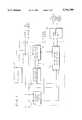
- FIG. 1is a block diagram of the elements of a write cache architecture according to the invention.
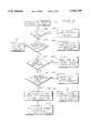
- FIG. 2is a functional flow diagram of the write sequence from a processor in a cache system with a level 1 cache and a write cache, according to the invention.
- FIG. 3is a flow diagram of the sequence involved in a burstwrite of a line to an external bus according to the invention in order to get data out from the cache.
- a write cache 5includes write cache storage area 10, copyback logic circuit 20, address comparator 30, and write cache controller 40.
- a level 1 (L1) cache 50is connected to the write cache 5 over internal buses 60, which include an internal address bus 61 and an internal data bus 62. Both the level 1 cache 50 and the write cache 5 are connected to a processor (not shown) over the internal buses 60.
- Cache storagecan be organized as lines, each line having a plurality of words. An address of a first word in a line can represent the address of the line.
- One way that burstwrites can be facilitatedis by indicating the address of a line of words to be the subject of a burstwrite.
- the write cache 5is preferably enabled only for a specific memory region.
- processor softwarecan be written to take advantage of the write cache 5 in desired applications, such as a graphics implementation or disk accelerator.
- specific software routineswhich can be changed to take advantage of the write cache features, are implemented without having an impact on the other processor software.
- restriction to a predetermined region of memoryis a limitation of the invention.
- the write cache controller 40controls all of the functions of the write cache 5 and interfaces with the level 1 cache 50.
- the write cache storage area 10stores data, a tag address for the data, and a status indication for the data.
- the write cache storage area 10is under control of the write cache controller 40.
- the address comparator 30compares an address received on the internal address bus 61 with a predetermined address range stored within the address comparator 30. If the address received on the internal address bus 61 falls within the predetermined address range, the address comparator 30 sends a signal to the write cache controller 40 indicating this "address range hit".
- the copyback logic circuit 20generates a request to the write cache controller 40 to copy a line corresponding to a specific address from the write cache storage area 10 to the external buses (not shown) upon detecting a burst write command from the processor. As discussed further herein, the physical address of the line to be copied back is written into the copyback logic circuit 20. The logic itself is selected by a specific address. During a write on the external buses, the copyback logic circuit 20 detects a write to a location and latches the physical address of the line to be copied back from the internal data bus 60. The copyback logic circuit 20 then indicates to the write cache controller 40 that a copyback needs to be initiated.
- the write cache 5only works on writes by the processor. When a read occurs, no operations are performed by the write cache 5.
- the write cache controller 40sees this write access and starts a cache look up to determine if the address corresponding to the write access is currently in the write cache storage area 10.
- the address comparator 30reads the address corresponding to the write access from the internal address bus 61 and determines if that address falls within a prespecified range of addresses for which the write cache 5 is programmed.
- the level 1 cache 50is also looking to see if it can service that write access.
- a processorinitiates a write request.
- the write cache controller 40begins a cache look up and an address range comparison.
- level 1 cache 50also begins a cache look up.
- the level 1 cache 50has a cache hit, as in step 202. If this is the case, the write request access address is resident in the level 1 cache 50 and the level 1 cache 50 services the request (step 204). No further operation is required of the write cache controller 40, and the sequence ends, as in step 206.
- the level 1 cache 50When the level 1 cache 50 has a cache hit, the level 1 cache 50 notifies the write cache 5 of this occurrence by sending a L1 -- Hit signal to the write cache controller 40, as can be seen from FIG. 1. Upon receipt of the L1 -- Hit signal, the write cache 5 knows that it is not to perform any further operations with respect to the write request.
- level 1 cache 50has a cache miss (i.e., no L1 -- Hit signal received by the write cache controller 40) and the requested write address, as determined by the address comparator 30, is not within the selected address region of the write cache 5, as shown in step 208 of FIG. 2. In this case, no further operation is required of the write cache controller 40, and the sequence ends, as in step 210.
- step 212is performed.
- the write requestis tested to determine if any of the tag addresses in the write cache 5 matches the request. This leads to third and fourth possible outcomes.
- the third possible outcomeis that the level 1 cache 50 has a cache miss (step 202), the requested write address, as determined by the address comparator 30, is within the selected address region of the write cache 5 (step 208), and the result of step 212 is that the write access hits the write cache 5.
- the write accessis stored in the appropriate storage area corresponding to the selected line in the write cache storage area 10, as in step 213. No external simple write is generated in this case.
- the fourth possibilityis that the level 1 cache 50 has a cache miss, the write access, as determined by the address comparator 30, is within the selected address region of the write cache 5, but that the outcome of step 212 is such that the write access does not hit the write cache 5.
- the write cacheis examined to determine if at least one storage area in the write cache storage area 10 is available to store the write access. Two outcomes are now possible.
- step 216the write cache controller 40 notifies the level 1 cache 50 that it stored the data corresponding to the write access. In this case, no external simple write, such as to the main memory, is generated.
- the write cache 5does not store the write access in its memory (step 220).
- the write cache 5notifies the level 1 cache 5 that it did not service the write access, as in step 222, for example, by sending a no hit signal to the L1 cache.
- a plurality of bitse.g., four bits per word, can be used to define which byte was written or modified. This is useful to avoid sending invalid data, as discussed further herein.
- the processor softwaremay want to initialize a burstwrite of data beginning at a specific address to the external bus.
- the processor softwareinitiates a single write to a copyback address register (not shown) in copyback logic circuit 20, as given in step 301 and places the physical address of the line to be copied on the internal bus.
- the copyback logic circuit 20itself is selected by a specific address. From the internal data bus 62, as given in step 302, the copyback address register 20 reads and latches the physical address of the write location (line) to be copied back.
- the copyback logic circuit 20notifies the write cache controller 40 of the burstwrite request from the processor, as given in step 303.
- the write cache controller 40responds to that burstwrite request by placing the selected line of the write cache 5 corresponding to the requested copyback access onto the external buses for a fast burstwrite, as given in step 304.
- the storage locations in the write cache storage area 10 that were dumped onto the external busesare freed up for the storage of new write requests from the processor, as given in step 306.
- the write cache controller 40keeps track of the available storage locations within the write cache 5, as given in step 307.
- the L1 cache 50performs the functions of a conventional cache memory and is not affected at all by the operation of the write cache 5. During write requests, the results of the address comparisons activate the functionality of the write cache 5 for a particular memory region. Address comparisons are performed in a processor or logic circuits within address comparator 30 implementing this function.
- the write cache controller 40which can be implemented in logic circuitry or in a processor, controls buffering and informs the L1 cache 50 that it need not respond to a particular write request by sending a signal over the WRC -- Hit Line connecting the L1 cache 50 to the write cache controller 40.
- the write cache controller 40can store information in a frame buffer memory for a video graphics accelerator, where one address of the frame buffer is followed by a plurality of data words or bytes to be sequentially transmitted in a burst in order to produce a display.
- the copyback logic circuit 20,which can also be implemented in logic circuitry or in a processor, is used to execute a burstwrite.
- the write cache 5is particularly useful in applications where streams of sequential data are written to memory.
- a display drivercan be written to draw four adjacent horizontal pixels. After four writes are performed into the write cache 5 without going to the external buses, the driver determines that it has completed its writes to the write cache 5 (assuming the write cache 5 is not full).
- a copybackis initiated through the copyback logic circuit 20.
- a complete address corresponding to a tag addressis written into the copyback logic circuit 20.
- the tag addressis the address of the data in the write cache 5 which is to be put on the external buses to accomplish the drawing.
- the copyback logic circuit 20retrieves from the internal bus 60 the address of the data to be sent to the bus interface unit 80 connected to the external buses, to thereby be sent to a particular address in the main memory (not shown) at a later time.
- a single burstwrite cyclecan transfer the information. For example, if line 1000 contains 16 bytes, addresses 1000 through 1015 are accessed as a burst. Thus, where all the pixels in one line are stored in sequential locations 1000 through 1015, it is only necessary to write address 1000 to the copyback logic circuit 20 to place all the data in locations 1000 through 1015 on the external bus to produce the display.
- Such a burstwritewhich can be achieved according to the invention, is far more efficient than a series of conventional individual writes.
- all writescan be stored in cache by using sequential writes in software, thus reducing the load on the cache.
Landscapes
- Engineering & Computer Science (AREA)
- Theoretical Computer Science (AREA)
- Physics & Mathematics (AREA)
- General Engineering & Computer Science (AREA)
- General Physics & Mathematics (AREA)
- Memory System Of A Hierarchy Structure (AREA)
Abstract
Description
Claims (4)
Priority Applications (4)
| Application Number | Priority Date | Filing Date | Title |
|---|---|---|---|
| US08/464,352US5761709A (en) | 1995-06-05 | 1995-06-05 | Write cache for servicing write requests within a predetermined address range |
| DE69618783TDE69618783T2 (en) | 1995-06-05 | 1996-06-04 | WRITE Cache to improve writing performance |
| PCT/US1996/008595WO1996039667A1 (en) | 1995-06-05 | 1996-06-04 | Write cache for write performance improvement |
| EP96917987AEP0835490B1 (en) | 1995-06-05 | 1996-06-04 | Write cache for write performance improvement |
Applications Claiming Priority (1)
| Application Number | Priority Date | Filing Date | Title |
|---|---|---|---|
| US08/464,352US5761709A (en) | 1995-06-05 | 1995-06-05 | Write cache for servicing write requests within a predetermined address range |
Publications (1)
| Publication Number | Publication Date |
|---|---|
| US5761709Atrue US5761709A (en) | 1998-06-02 |
Family
ID=23843598
Family Applications (1)
| Application Number | Title | Priority Date | Filing Date |
|---|---|---|---|
| US08/464,352Expired - LifetimeUS5761709A (en) | 1995-06-05 | 1995-06-05 | Write cache for servicing write requests within a predetermined address range |
Country Status (4)
| Country | Link |
|---|---|
| US (1) | US5761709A (en) |
| EP (1) | EP0835490B1 (en) |
| DE (1) | DE69618783T2 (en) |
| WO (1) | WO1996039667A1 (en) |
Cited By (13)
| Publication number | Priority date | Publication date | Assignee | Title |
|---|---|---|---|---|
| WO2000017873A1 (en)* | 1998-09-24 | 2000-03-30 | Zen Research (Ireland), Ltd. | Method and apparatus for buffering data in a multi-beam optical disk reader |
| US20020029354A1 (en)* | 2000-08-23 | 2002-03-07 | Seagate Technology Llc | Non-volatile write cache, in a disc drive, using an alternate power source |
| US6437789B1 (en)* | 1999-02-19 | 2002-08-20 | Evans & Sutherland Computer Corporation | Multi-level cache controller |
| US20030181994A1 (en)* | 2002-03-19 | 2003-09-25 | Fujitsu Limited | Microprocessor performing efficient external bus access |
| US7689766B1 (en)* | 2005-06-10 | 2010-03-30 | American Megatrends, Inc. | Method, system, apparatus, and computer-readable medium for integrating a caching module into a storage system architecture |
| US7891818B2 (en) | 2006-12-12 | 2011-02-22 | Evans & Sutherland Computer Corporation | System and method for aligning RGB light in a single modulator projector |
| US8077378B1 (en) | 2008-11-12 | 2011-12-13 | Evans & Sutherland Computer Corporation | Calibration system and method for light modulation device |
| US8352716B1 (en) | 2008-01-16 | 2013-01-08 | American Megatrends, Inc. | Boot caching for boot acceleration within data storage systems |
| US8358317B2 (en) | 2008-05-23 | 2013-01-22 | Evans & Sutherland Computer Corporation | System and method for displaying a planar image on a curved surface |
| US8549230B1 (en) | 2005-06-10 | 2013-10-01 | American Megatrends, Inc. | Method, system, apparatus, and computer-readable medium for implementing caching in a storage system |
| US8702248B1 (en) | 2008-06-11 | 2014-04-22 | Evans & Sutherland Computer Corporation | Projection method for reducing interpixel gaps on a viewing surface |
| US9641826B1 (en) | 2011-10-06 | 2017-05-02 | Evans & Sutherland Computer Corporation | System and method for displaying distant 3-D stereo on a dome surface |
| US10705853B2 (en) | 2008-05-06 | 2020-07-07 | Amzetta Technologies, Llc | Methods, systems, and computer-readable media for boot acceleration in a data storage system by consolidating client-specific boot data in a consolidated boot volume |
Citations (7)
| Publication number | Priority date | Publication date | Assignee | Title |
|---|---|---|---|---|
| EP0325420A2 (en)* | 1988-01-20 | 1989-07-26 | Advanced Micro Devices, Inc. | Organization of an integrated cache unit for flexible usage in cache system design |
| EP0470735A1 (en)* | 1990-08-06 | 1992-02-12 | NCR International, Inc. | Computer memory system |
| US5197144A (en)* | 1990-02-26 | 1993-03-23 | Motorola, Inc. | Data processor for reloading deferred pushes in a copy-back data cache |
| EP0602807A2 (en)* | 1992-12-18 | 1994-06-22 | Advanced Micro Devices, Inc. | Cache memory systems |
| EP0602808A2 (en)* | 1992-12-18 | 1994-06-22 | Advanced Micro Devices, Inc. | Cache systems |
| US5325499A (en)* | 1990-09-28 | 1994-06-28 | Tandon Corporation | Computer system including a write protection circuit for preventing illegal write operations and a write poster with improved memory |
| US5359723A (en)* | 1991-12-16 | 1994-10-25 | Intel Corporation | Cache memory hierarchy having a large write through first level that allocates for CPU read misses only and a small write back second level that allocates for CPU write misses only |
- 1995
- 1995-06-05USUS08/464,352patent/US5761709A/ennot_activeExpired - Lifetime
- 1996
- 1996-06-04EPEP96917987Apatent/EP0835490B1/ennot_activeExpired - Lifetime
- 1996-06-04WOPCT/US1996/008595patent/WO1996039667A1/enactiveIP Right Grant
- 1996-06-04DEDE69618783Tpatent/DE69618783T2/ennot_activeExpired - Lifetime
Patent Citations (9)
| Publication number | Priority date | Publication date | Assignee | Title |
|---|---|---|---|---|
| EP0325420A2 (en)* | 1988-01-20 | 1989-07-26 | Advanced Micro Devices, Inc. | Organization of an integrated cache unit for flexible usage in cache system design |
| US5197144A (en)* | 1990-02-26 | 1993-03-23 | Motorola, Inc. | Data processor for reloading deferred pushes in a copy-back data cache |
| EP0470735A1 (en)* | 1990-08-06 | 1992-02-12 | NCR International, Inc. | Computer memory system |
| US5325499A (en)* | 1990-09-28 | 1994-06-28 | Tandon Corporation | Computer system including a write protection circuit for preventing illegal write operations and a write poster with improved memory |
| US5359723A (en)* | 1991-12-16 | 1994-10-25 | Intel Corporation | Cache memory hierarchy having a large write through first level that allocates for CPU read misses only and a small write back second level that allocates for CPU write misses only |
| EP0602807A2 (en)* | 1992-12-18 | 1994-06-22 | Advanced Micro Devices, Inc. | Cache memory systems |
| EP0602808A2 (en)* | 1992-12-18 | 1994-06-22 | Advanced Micro Devices, Inc. | Cache systems |
| US5502828A (en)* | 1992-12-18 | 1996-03-26 | Advanced Micro Devices, Inc. | Reducing memory access in a multi-cache multiprocessing environment with each cache mapped into different areas of main memory to avoid contention |
| US5524225A (en)* | 1992-12-18 | 1996-06-04 | Advanced Micro Devices Inc. | Cache system and method for providing software controlled writeback |
Non-Patent Citations (4)
| Title |
|---|
| Anon., "Dynamic Memory Architecture Increases Performance of 486-Based Motherboards", Electronic Design, vol. 41, No. 15, Jul. 1993, pp. 36-38. |
| Anon., Dynamic Memory Architecture Increases Performance of 486 Based Motherboards , Electronic Design, vol. 41, No. 15, Jul. 1993, pp. 36 38.* |
| Chen, Yung Chin and Veidenbaum, Alexander V. An Effective Write Policy for Software Coherence Schemes , IEEE Computer Society Press, 1992; pp. 661 72.* |
| Chen, Yung-Chin and Veidenbaum, Alexander V. "An Effective Write Policy for Software Coherence Schemes", IEEE Computer Society Press, 1992; pp. 661-72. |
Cited By (18)
| Publication number | Priority date | Publication date | Assignee | Title |
|---|---|---|---|---|
| WO2000017873A1 (en)* | 1998-09-24 | 2000-03-30 | Zen Research (Ireland), Ltd. | Method and apparatus for buffering data in a multi-beam optical disk reader |
| US6137763A (en)* | 1998-09-24 | 2000-10-24 | Zen Research N.V. | Method and apparatus for buffering data in a multi-beam optical disk reader |
| US6437789B1 (en)* | 1999-02-19 | 2002-08-20 | Evans & Sutherland Computer Corporation | Multi-level cache controller |
| US20020029354A1 (en)* | 2000-08-23 | 2002-03-07 | Seagate Technology Llc | Non-volatile write cache, in a disc drive, using an alternate power source |
| US20030181994A1 (en)* | 2002-03-19 | 2003-09-25 | Fujitsu Limited | Microprocessor performing efficient external bus access |
| US8307155B1 (en) | 2005-06-10 | 2012-11-06 | American Megatrends, Inc. | Method, system, apparatus, and computer-readable medium for integrating a caching module into a storage system architecture |
| US7689766B1 (en)* | 2005-06-10 | 2010-03-30 | American Megatrends, Inc. | Method, system, apparatus, and computer-readable medium for integrating a caching module into a storage system architecture |
| US8549230B1 (en) | 2005-06-10 | 2013-10-01 | American Megatrends, Inc. | Method, system, apparatus, and computer-readable medium for implementing caching in a storage system |
| US8850124B1 (en) | 2005-06-10 | 2014-09-30 | American Megatrends, Inc. | Method, system, apparatus, and computer-readable medium for implementing caching in a storage system |
| US7891818B2 (en) | 2006-12-12 | 2011-02-22 | Evans & Sutherland Computer Corporation | System and method for aligning RGB light in a single modulator projector |
| US8352716B1 (en) | 2008-01-16 | 2013-01-08 | American Megatrends, Inc. | Boot caching for boot acceleration within data storage systems |
| US8775786B1 (en) | 2008-01-16 | 2014-07-08 | American Megatrends, Inc. | Boot caching for boot acceleration within data storage systems |
| US10705853B2 (en) | 2008-05-06 | 2020-07-07 | Amzetta Technologies, Llc | Methods, systems, and computer-readable media for boot acceleration in a data storage system by consolidating client-specific boot data in a consolidated boot volume |
| US8358317B2 (en) | 2008-05-23 | 2013-01-22 | Evans & Sutherland Computer Corporation | System and method for displaying a planar image on a curved surface |
| US8702248B1 (en) | 2008-06-11 | 2014-04-22 | Evans & Sutherland Computer Corporation | Projection method for reducing interpixel gaps on a viewing surface |
| US8077378B1 (en) | 2008-11-12 | 2011-12-13 | Evans & Sutherland Computer Corporation | Calibration system and method for light modulation device |
| US9641826B1 (en) | 2011-10-06 | 2017-05-02 | Evans & Sutherland Computer Corporation | System and method for displaying distant 3-D stereo on a dome surface |
| US10110876B1 (en) | 2011-10-06 | 2018-10-23 | Evans & Sutherland Computer Corporation | System and method for displaying images in 3-D stereo |
Also Published As
| Publication number | Publication date |
|---|---|
| EP0835490B1 (en) | 2002-01-23 |
| EP0835490A1 (en) | 1998-04-15 |
| DE69618783T2 (en) | 2002-08-29 |
| WO1996039667A1 (en) | 1996-12-12 |
| DE69618783D1 (en) | 2002-03-14 |
Similar Documents
| Publication | Publication Date | Title |
|---|---|---|
| KR100252570B1 (en) | Cache memory with reduced request-blocking | |
| US5829032A (en) | Multiprocessor system | |
| US6542968B1 (en) | System and method for managing data in an I/O cache | |
| US6434639B1 (en) | System for combining requests associated with one or more memory locations that are collectively associated with a single cache line to furnish a single memory operation | |
| US5627993A (en) | Methods and systems for merging data during cache checking and write-back cycles for memory reads and writes | |
| US5185694A (en) | Data processing system utilizes block move instruction for burst transferring blocks of data entries where width of data blocks varies | |
| US6718441B2 (en) | Method to prefetch data from system memory using a bus interface unit | |
| US6321296B1 (en) | SDRAM L3 cache using speculative loads with command aborts to lower latency | |
| US5423016A (en) | Block buffer for instruction/operand caches | |
| JP2509766B2 (en) | Cache memory exchange protocol | |
| US5561783A (en) | Dynamic cache coherency method and apparatus using both write-back and write-through operations | |
| JPH10504124A (en) | Two-way set associative cache memory | |
| US5761709A (en) | Write cache for servicing write requests within a predetermined address range | |
| US5479636A (en) | Concurrent cache line replacement method and apparatus in microprocessor system with write-back cache memory | |
| US5850534A (en) | Method and apparatus for reducing cache snooping overhead in a multilevel cache system | |
| US5724547A (en) | LRU pointer updating in a controller for two-way set associative cache | |
| JPH08185355A (en) | Data memory and its operating method | |
| US5678025A (en) | Cache coherency maintenance of non-cache supporting buses | |
| US5974497A (en) | Computer with cache-line buffers for storing prefetched data for a misaligned memory access | |
| US6434665B1 (en) | Cache memory store buffer | |
| US5987570A (en) | Performing overlapping burst memory accesses and interleaved memory accesses on cache misses | |
| US6008823A (en) | Method and apparatus for enhancing access to a shared memory | |
| JPH06318174A (en) | Cache memory system and method for performing cache for subset of data stored in main memory | |
| US6044441A (en) | Method and apparatus for encoding valid and invalid states in a cache with an invalid pattern | |
| US6098151A (en) | Cache memory control system that caches requested data and adjacently displayed data |
Legal Events
| Date | Code | Title | Description |
|---|---|---|---|
| FEPP | Fee payment procedure | Free format text:PAYOR NUMBER ASSIGNED (ORIGINAL EVENT CODE: ASPN); ENTITY STATUS OF PATENT OWNER: LARGE ENTITY | |
| AS | Assignment | Owner name:ADVANCED MICRO DEVICES INC., CALIFORNIA Free format text:ASSIGNMENT OF ASSIGNORS INTEREST;ASSIGNOR:KRANICH, UWE;REEL/FRAME:008918/0765 Effective date:19971216 | |
| STCF | Information on status: patent grant | Free format text:PATENTED CASE | |
| AS | Assignment | Owner name:LEGERITY, INC., TEXAS Free format text:ASSIGNMENT OF ASSIGNORS INTEREST;ASSIGNOR:ADVANCED MICRO DEVICES, INC.;REEL/FRAME:011700/0686 Effective date:20000731 | |
| FPAY | Fee payment | Year of fee payment:4 | |
| AS | Assignment | Owner name:MORGAN STANLEY & CO. INCORPORATED, AS FACILITY COL Free format text:SECURITY AGREEMENT;ASSIGNORS:LEGERITY, INC.;LEGERITY HOLDINGS, INC.;LEGERITY INTERNATIONAL, INC.;REEL/FRAME:013372/0063 Effective date:20020930 | |
| FPAY | Fee payment | Year of fee payment:8 | |
| AS | Assignment | Owner name:SAXON IP ASSETS LLC, TEXAS Free format text:ASSIGNMENT OF ASSIGNORS INTEREST;ASSIGNOR:LEGERITY, INC.;REEL/FRAME:017537/0307 Effective date:20060324 | |
| AS | Assignment | Owner name:LEGERITY HOLDINGS, INC., TEXAS Free format text:RELEASE OF SECURITY INTEREST;ASSIGNOR:MORGAN STANLEY SENIOR FUNDING INC., AS ADMINISTRATIVE AGENT, SUCCESSOR TO MORGAN STANLEY & CO. INCORPORATED, AS FACILITY COLLATERAL AGENT;REEL/FRAME:019699/0854 Effective date:20070727 Owner name:LEGERITY, INC., TEXAS Free format text:RELEASE OF SECURITY INTEREST;ASSIGNOR:MORGAN STANLEY SENIOR FUNDING INC., AS ADMINISTRATIVE AGENT, SUCCESSOR TO MORGAN STANLEY & CO. INCORPORATED, AS FACILITY COLLATERAL AGENT;REEL/FRAME:019699/0854 Effective date:20070727 Owner name:LEGERITY INTERNATIONAL, INC., TEXAS Free format text:RELEASE OF SECURITY INTEREST;ASSIGNOR:MORGAN STANLEY SENIOR FUNDING INC., AS ADMINISTRATIVE AGENT, SUCCESSOR TO MORGAN STANLEY & CO. INCORPORATED, AS FACILITY COLLATERAL AGENT;REEL/FRAME:019699/0854 Effective date:20070727 | |
| AS | Assignment | Owner name:SAXON INNOVATIONS, LLC, TEXAS Free format text:ASSIGNMENT OF ASSIGNORS INTEREST;ASSIGNOR:SAXON IP ASSETS, LLC;REEL/FRAME:020072/0432 Effective date:20071016 | |
| AS | Assignment | Owner name:LG ELECTRONICS INC., KOREA, REPUBLIC OF Free format text:ASSIGNMENT OF ASSIGNORS INTEREST;ASSIGNOR:SAXON INNOVATIONS, LLC;REEL/FRAME:023129/0837 Effective date:20090806 | |
| FPAY | Fee payment | Year of fee payment:12 | |
| FEPP | Fee payment procedure | Free format text:PAYER NUMBER DE-ASSIGNED (ORIGINAL EVENT CODE: RMPN); ENTITY STATUS OF PATENT OWNER: LARGE ENTITY Free format text:PAYOR NUMBER ASSIGNED (ORIGINAL EVENT CODE: ASPN); ENTITY STATUS OF PATENT OWNER: LARGE ENTITY |