US5761064A - Defect management system for productivity and yield improvement - Google Patents
Defect management system for productivity and yield improvementDownload PDFInfo
- Publication number
- US5761064A US5761064AUS08/539,913US53991395AUS5761064AUS 5761064 AUS5761064 AUS 5761064AUS 53991395 AUS53991395 AUS 53991395AUS 5761064 AUS5761064 AUS 5761064A
- Authority
- US
- United States
- Prior art keywords
- wafer
- data
- defect data
- wafer defect
- converted
- Prior art date
- Legal status (The legal status is an assumption and is not a legal conclusion. Google has not performed a legal analysis and makes no representation as to the accuracy of the status listed.)
- Expired - Lifetime
Links
Images


Classifications
- H—ELECTRICITY
- H01—ELECTRIC ELEMENTS
- H01L—SEMICONDUCTOR DEVICES NOT COVERED BY CLASS H10
- H01L22/00—Testing or measuring during manufacture or treatment; Reliability measurements, i.e. testing of parts without further processing to modify the parts as such; Structural arrangements therefor
- H01L22/20—Sequence of activities consisting of a plurality of measurements, corrections, marking or sorting steps
- G—PHYSICS
- G01—MEASURING; TESTING
- G01R—MEASURING ELECTRIC VARIABLES; MEASURING MAGNETIC VARIABLES
- G01R31/00—Arrangements for testing electric properties; Arrangements for locating electric faults; Arrangements for electrical testing characterised by what is being tested not provided for elsewhere
- G01R31/28—Testing of electronic circuits, e.g. by signal tracer
- G01R31/317—Testing of digital circuits
- G01R31/3181—Functional testing
- G01R31/319—Tester hardware, i.e. output processing circuits
Definitions
- This inventionrelates generally to semiconductor wafer manufacturing, and, more particularly, to an automated semiconductor wafer defect management system for productivity and yield improvement.
- the microscopic dimensions capabilities of current semiconductor manufacturing equipmentmake possible the design of digital circuits which may be very complex and yet extremely economical in space, power requirements and cost, and which are potentially very fast.
- the microscopic dimensions of current semiconductor manufacturingalso make it possible for microscopic particles to contaminate and ruin an extended run of wafers before the contamination is discovered causing major economic loss. It is therefore critical that there is a method to discover, not only that there are defects in the wafer manufacturing process, but to determine exactly what is causing those defects. To avoid extensive economic loss it is mandatory to discover these defects as quickly as possible and as close to real time as possible.
- wafer inspection and failure analysis toolsprovide detailed qualitative and quantitative information about processing defects and the failures caused by them.
- each wafer inspection toolproduces information not easily accessible to the production process engineering community.
- analytical instrumentsproduce data faster than can be manually analyzed by engineers.
- the first step in the developmental processwas to define the functional specifications desired in the system.
- the final requirementsincluded detailed specifications for every feature and operation of a fully-automated, on-line system.
- the first functional specificationconcerned connectivity. It was determined that an automated system must: (1) provide for the inter-operability of multiple vendor equipment, including the ability to integrate all data and to provide access to the integrated data back to any vendor's review station in its native format; (2) provide a data translation facility to accommodate native data formats, changes, and new tools; and (3) provide total data access time from user workstation or from any vendor's instrument review station of not more than three seconds with multiple users on-line simultaneously.
- the second functional requirementconcerned data manipulation, charting, and reporting capabilities.
- the automated systemmust: (1) allow any combination of data identifier parameters drawn from the workstream (including such parameters as which wafer is being examined, which process technology was used to make the wafer, which inspection device is being used, which layer in the wafer is being examined, and which lot the wafer was from) to be displayed in multiple trend charts and sub-charts simultaneously; (2) allow x-axis and y-axis to be user configurable; and (3) perform statistical calculations automatically for any data combination.
- the automated systemmust: (1) provide a simple, graphical user interface with point-and-click menu options and minimal text entries; (2) allow wafer maps, die maps, and layer images to be overlaid at any magnification (e.g., composite wafer maps of in-line and bitmap data); (3) support filtering options by defect type, defect size, intensity or other user-specified data type; and (4) display multiple bitmap images and electrical failure "bin" data simultaneously, allowing access to defect images and analysis data through wafer maps.
- the final functional requirementconcerned system security, safety, and maintenance. It was determined that the system must: (1) provide for password security access by type of user, such as technician, engineer, or systems administrator; (2) provide automatic back-up data integrity in case of system (computer or storage) failure, power outage, or network crash; and (3) support remote system and network administration.
- an automated wafer defect management systemin which wafer defect data are collected from wafer inspection instruments, converted into a standard data format, and transferred to a central database system.
- user interface workstationssuch that users can select information and have it transferred to the workstation for review.
- the user at each workstationcan have the workstation create statistical and graphical representations of the selected data for review at the workstation.
- the usercan select a single or multiple overlaid statistical and graphical representations by pointing-and-clicking on a data point in a displayed chart.
- the format for displaycan be selected by the user and can be a trend chart, an optical image, a secondary electron microscope image, a wafer map, a tool comparison chart or a Pareto chart or a combination of any of the above shown in a WindowsTM display.
- wafer defect dataare transferred to data analysis stations which perform detailed analysis of the wafer defect data and return the analyzed data to the central database system.
- the data analysis stationsinclude the capability for defect classification, image capture, surface/cross-section analysis, and spectral analysis.
- the detailed analysis generated by the data analysis stationsis also available for review, study, and evaluation at each workstation.
- the central database systemis made up of a relational database installed on a server with memory to store the wafer defect data.
- the relational databaseorganizes the wafer defect data in tables where it is tagged according to preselected criteria.
- the preselected criteriaincludes process technology, layer, lot, wafer, device, process equipment identification, and scan tool identification.
- the central database systemcan access databases containing electrical test results and in-line process monitor and equipment monitor information which is correlated to the pertinent wafer defect data. This correlated data is available for review at the user interface workstations.
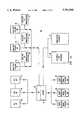
- FIG. 1Ashows a first embodiment of the automated wafer defect management system of the present invention.
- FIG. 1Bshows a second embodiment of the automated wafer defect management system of the present invention.
- FIG. 2shows an embodiment of the automated wafer defect management system showing representative components in accordance with the present invention.
- FIG. 3shows selected display attributes provided by the present invention.
- FIG. 4illustrates the point-and-click capabilities of the present invention.
- FIG. 5shows a layer trend chart for percent bad dies per week.
- FIG. 6shows a box chart for percent bad dies per layer in the wafer.
- FIG. 7shows a box chart for percent bad dies per week.
- FIG. 8shows a layer comparison chart for percent bad dies per week.
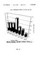
- FIG. 9shows a layer bar chart for defect count per layer.
- FIG. 10shows a layer bar chart for percent bad dies per layer.
- FIG. 1AOne embodiment of the present invention is illustrated in FIG. 1A.
- a wafer defect management system 20In this embodiment there is shown wafer inspection instrument (WII #1) 22, wafer inspection instrument (WII#2) 24, and wafer inspection instrument (WII #1) 26 representing that multiple wafer inspection instruments may be connected to the system.
- the wafer inspection instruments 22,24,26are connected to a conversion box (CB) 28 which is shown connected to server 30.
- CBconversion box
- This embodimentalso shows analysis station (#1) 32, analysis station (#2) 34, and analysis station (#m) 36 representing that multiple analysis stations may be connected to the system.
- Each analysis stationmay have associated with it an analysis PC workstation as shown at 38, 40 and 42.
- This embodimentalso shows user interface workstation (#1) 44, user interface workstation (#2) 46, and user interface workstation (#n) 48 representing that multiple user interface workstations may be connected to the system.
- An electrical test database 50 and a workstream database 52are also shown connected to the server 30.
- FIG. 1Bshows another embodiment of the present invention similar to the embodiment shown in FIG. 1A and wherein like component have the same numerical designations.
- conversion boxes 54,56,58associated with wafer inspection instruments 22,24,26 respectively and conversion boxes 60,62,64 associated with analysis stations 32,34,36 respectively.
- the conversion boxes 64are desktop computers equipped with specialized hardware and software to translate all the information provided by each attached instrument into a standard format.
- the conversion boxes 54-64handle video data digitizing, file transfer and communications between each attached instrument and the server 30.
- Software in the respective conversion boxes 54-64converts data from the attached instrument's native format into a standard Transmission Control Program/Internet Protocol (TCP/IP) format.
- TCP/IPTransmission Control Program/Internet Protocol
- the respective conversion box 54-64then transfers the data using TCP/IP's File Transfer Protocol (FTP) to the server 30.
- TCP/IPTransmission Control Program/Internet Protocol
- FTPFile Transfer Protocol
- FIG. 2there is shown a representative defect wafer management system 65 utilizing the teaching of the present invention and is considered by the inventors as the best mode of the invention as of the filing date.
- This embodimentutilizes an ethernet backbone 66 to network a sort station 68, a fab 70, an analysis lab 72, and engineering 74.
- a wafer sort test station 76sorts and tests wafers and sends data via conversion box 78 and Ethernet 66 to server 80.
- Server 80 in the representative system 65is a Hewlett Packard (HP) Apollo 735 server running Oracle Version 7.0 database. Oracle Version 7.0 was chosen for representative system 65 because of its powerful relational database. As can be appreciated other equivalent servers could be used as well as other equivalent database software programs.
- Disk storage 82consists of ten gigabytes and provides data record access time of less than 15 ms.
- the wafer inspection instruments in the Fab 70comprise an Estek 8500 shown at 84, an Inspex 8510 shown at 86, a Seiko SEM/EDX (scanned electron microscopy/energy dispersive x-ray) shown at 88, a KLA 2131 shown at 90, and a KLA 2550 shown at 92.
- the Estek instrument 84 and the Inspex 86 instrumenteach have a conversion box 94,96 respectively, each connected to Ethernet 66.
- the Seiko 88 instrumenthas an analysis station 98 which is connected to Ethernet 66 via a conversion box 104.
- the KLA 2131 instrument 90 and the KLA 2550 instrument 92share a review station 102 which is connected to Ethernet 66 via conversion box 108.
- the KLA 2131 instrument 90, the Inspex 8610 instrument 86, and the Estek 8500 instrument 84are wafer scanning tools which detect defects and anomalies in the wafers.
- KLA 2550 review station 92is an optical microscopic review tool to review and capture optical images of defects on a wafer after the wafer has been scanned by an inspection station.
- the analysis stations 102,98are analytical tools to perform surface analyses and cross-section analyses (by ion-milling) and can provide electron and ion micrographs of defects and can perform compositional analysis of defects.
- Analysis lab 72shows a Seiko FIB 110 with an analysis station 112 and a conversion box 114 connected to Ethernet 66 and a microscope & stage unit 116 connected to a bitmap stage controller 118 which is connected to Ethernet 66. Analysis lab 72 also shows PC workstations 120 and 122 connected to Ethernet 66.
- Engineering 74show two PC user interface workstations 124 and 126 connected to Ethernet 66. As discussed above Engineering 74 can support multiple user interface workstations which can be distributed throughout the corporation limited only by the availability of an Ethernet 66 connection.
- the operation of representative system 68is as follows.
- the central database system installed on server 80acquires information in real time from every inspection and analysis tool in use throughout system 68. Data is stored in tables organized according to how it is called up by the user interface and tagged according to: process technology, layer, lot, wafer, device, process equipment identification, and scan tool identification. Data is automatically backed-up and archived by the Oracle software installed on server 80. A partial archive is taken daily and a full archive tape is removed from the system once each month.
- the PC user interface workstations 124,126are 486-based workstations running WindowsTM. These workstation are configured with 8 Mb of memory, at least a 120 Mb hard drive, an Ethernet card running TCP/IP and FTP software, and SQL*NET.
- Unformatted datamove across the network efficiently in TCP/IP packets to and from the Oracle database, and to the workstations 120,122,124,126 where custom software created by Inspex creates graphic representations and statistical calculations independently of both the network and the central database. Off-loading the graphical processing from the server onto the respective workstation provides for the fastest user response time while at the same time conserving network resources.
- Workstations 120,122,124,126receive user selected wafer data from the central database server 80. Then, using a point-and-click graphical interface, the user can view the selected data as trend charts, images, wafer maps, tool comparisons and Pareto charts.
- the data retrieval operations and graphical presentationsare generated on workstations 120,122,124,126 in less than three seconds.
- each workstationhas the capability of displaying multiple graphical representations there is no need to create a paper record.
- the only need for a paper reportis for management reporting purposes and a paper report can be printed outside the clean room environment.
- Trend charts and other graphical representations of the datacan be selected on the desktop workstations by mouse-driven or menu options commands. Text data fields are also provided, with textual data becoming part of the wafer defect database.
- FIG. 3there is shown a representation of the information that is obtainable by a user at a user interface workstation.
- the usercan select specific wafer defect data that needs to be examined.
- the usercan chose a box plot 128 which compares defect level of any inspected layer between different lots or for different workweeks, a stacked bar chart 130 which shows defect level distribution of inspected layers, a yield to defect density correlation chart 132 which is an x-y scatter plot of wafer sort yield versus defect density, a defect Pareto chart 134 which shows defect type distribution of inspected layers in a given time frame, or a statistical process control chart (SPC) 136 where x-axis represents lot ID's and the y-axis represents percent bad die.
- SPCstatistical process control chart
- CL 138is the center line which is equal to the average of all data points in the chart.
- UCL 140is the upper control limit which is equal to CL+3*standard deviation.
- the SPC 136is monitored closely for indications of problem lots which are indicated by any data point above UCL 140. Once a problem is detected on the SPC 136 the user double clicks on the data point on the chart, for example, data point 139 on SPC 136. This generates the pertinent defect wafer map 140.
- the arrows 142indicate that the defect wafer map 140 is generated by double-clicking on data point 139.
- the defect wafer mapshows each individual die and a dot on each die in which there is a defect. The user can select any defect on any die for further examination by double-clicking on that defect.
- defect wafer map 140shows a representative defect 144 which has been double-clicked (indicated by arrows 146) for further examination.
- the next chart generatedis a defect optical image chart 148 of the defect in the selected die.
- the next chart generatedis a scanning electron microscope (SEM) image 150. The user can then select a spectral analysis chart 152 of the wafer defect selected.
- SEMscanning electron microscope
- the user at a user interface workstationcan click on the chart to request wafer defect maps from the processing lot being analyzed.
- any analysis performed on the subject defecti.e., SEM (scanning electron microscopy) or FIB (focused ion beam) images, EDX (energy dispersive x-ray) elemental analysis or FIB milling results, are available within seconds.
- the usermerely clicks on the desired choice to move from screen to screen, as shown in FIG. 3.
- FIG. 4is a larger scale illustration of the wafer defect map shown in FIG. 3 and the possible graphical representations that can be selected by the user.
- the usercan select any defect for further examination.
- the defect shown at 156is selected for further examination by double-clicking on the defect represented by arrows 158. This generates defect optical image 160.
- a scanning electron microscope (SEM) image 165is generated.
- SEMscanning electron microscope
- FIG. 5shows a layer trend chart for percent bad dies 170.
- the x-axisshows weeks and the y-axis show percent defective dies.
- the layer trend chart 170can be generated for various parameters such as which scan tools were utilized, which process technology was used, and for layer.
- a moving averageis indicated at 172.
- FIG. 6is a box chart for percent bad dies with the x-axis indicating layers and the y-axis indicating percent defective dies.
- the box chartcan be generated for specific parameters, such as which scan tools, which process technology, device, and which layers.
- FIG. 7is a box chart similar to the box chart of FIG. 6, however, the box chart in FIG. 7 has the x-axis showing weeks and the y-axis showing percent defective dies. The parameters are the same except that the chart is generated using a specific layer.
- FIG. 8shows a layer comparison chart for percent bad dies with the x-axis showing weeks and the y-axis showing percent defective dies. Again the chart can be generated with specified parameters such as which scan tools, which process technology, and which devices were utilized.
- FIG. 9shows a layer bar chart for defect count per layer.
- the x-axisshows layers and the y-axis shows number of defect count.
- the parameters for the chartcan be selected by the user and include which scan tools, which process technology, and which devices.
- FIG. 10shows a layer bar chart for percent bad dies with the x-axis showing layers and the y-axis showing percent defective dies.
- the parameters for this chartcan be selected and in this chart include which scan tools, which process technology, and which devices.
Landscapes
- Engineering & Computer Science (AREA)
- Manufacturing & Machinery (AREA)
- Computer Hardware Design (AREA)
- Microelectronics & Electronic Packaging (AREA)
- Power Engineering (AREA)
- General Engineering & Computer Science (AREA)
- Physics & Mathematics (AREA)
- General Physics & Mathematics (AREA)
- Testing Or Measuring Of Semiconductors Or The Like (AREA)
Abstract
Description
1. Field of the Invention
This invention relates generally to semiconductor wafer manufacturing, and, more particularly, to an automated semiconductor wafer defect management system for productivity and yield improvement.
2. Discussion of the Related Art
Growing technological requirements and the worldwide acceptance of sophisticated electronic devices have created an unprecedented demand for large-scale, complex, integrated circuits. Meeting these demands has required technological advances in materials and processing equipment, significant increases in the number of individuals involved in integrated circuit design, and an increased emphasis on effectively utilizing the computer and other highly sophisticated equipment to aid, not only in the design, but in the analysis of the manufacturing process.
The microscopic dimensions capabilities of current semiconductor manufacturing equipment make possible the design of digital circuits which may be very complex and yet extremely economical in space, power requirements and cost, and which are potentially very fast. At the same time, however, the microscopic dimensions of current semiconductor manufacturing also make it possible for microscopic particles to contaminate and ruin an extended run of wafers before the contamination is discovered causing major economic loss. It is therefore critical that there is a method to discover, not only that there are defects in the wafer manufacturing process, but to determine exactly what is causing those defects. To avoid extensive economic loss it is mandatory to discover these defects as quickly as possible and as close to real time as possible.
The character of the semiconductor industry is such that competition requires that products are designed, manufactured, and marketed in the most efficient manner possible. This has required that improvements in fabrication technology keep pace with the rapid improvements in the electronics industry.
As advances in semiconductor wafer manufacturing technology lead to more sophisticated instruments with improved imaging and analysis capabilities, the volume of data associated with these instruments has grown faster than the ability of standard methods of analysis making wafer defect management on a timely basis problematic.
Present wafer inspection and failure analysis tools provide detailed qualitative and quantitative information about processing defects and the failures caused by them. However, each wafer inspection tool produces information not easily accessible to the production process engineering community. In a well equipped semiconductor wafer manufacturing fab, analytical instruments produce data faster than can be manually analyzed by engineers.
Making semiconductor wafer defect and contamination data available on a timely basis throughout the corporate engineering community has become just as important, if not more important than obtaining the data in the first place.
The problem is exacerbated by the fact that the intelligence (the controls, user interface, and data management capabilities) integrated into each instrument is dedicated to that instrument. Vendors have developed proprietary methods for collecting, processing, storing, and outputting data, and have not established a single set of standards for combining data from multiple vendor equipment. Because of this, engineers have had to use one stand-alone tool at a time making it virtually impossible to efficiently correlate wafer defect information concerning the same wafer.
Because there was no method to correlate wafer defect information, another significant problem was that analytical results was invariably reduced to the form of paper output--even through converted into compact representations such as charts, graphs, or high-resolution images. This reduction to paper was necessary because there was not a method to correlate all the information in one format for efficient presentation. In addition, not only is paper an inefficient medium for distributing information, it is also a serious source of contamination in ultraclean manufacturing environments. Paper fiber, or dust, can contaminate wafers during manufacturing.
Because of the problems associated with wafer defect management the inventors were tasked to obtain an automated system that would network all wafer defect analysis instruments and enable any engineer to access wafer defect data on-line from the engineer's desk without handling paper. After an intensive search the inventors were unable to find an existing solution. The inventors were then tasked to undertake a study to determine the feasibility of developing an automated system.
The first step in the developmental process was to define the functional specifications desired in the system. The final requirements included detailed specifications for every feature and operation of a fully-automated, on-line system.
The first functional specification concerned connectivity. It was determined that an automated system must: (1) provide for the inter-operability of multiple vendor equipment, including the ability to integrate all data and to provide access to the integrated data back to any vendor's review station in its native format; (2) provide a data translation facility to accommodate native data formats, changes, and new tools; and (3) provide total data access time from user workstation or from any vendor's instrument review station of not more than three seconds with multiple users on-line simultaneously.
The second functional requirement concerned data manipulation, charting, and reporting capabilities. The automated system must: (1) allow any combination of data identifier parameters drawn from the workstream (including such parameters as which wafer is being examined, which process technology was used to make the wafer, which inspection device is being used, which layer in the wafer is being examined, and which lot the wafer was from) to be displayed in multiple trend charts and sub-charts simultaneously; (2) allow x-axis and y-axis to be user configurable; and (3) perform statistical calculations automatically for any data combination.
The third functional requirement concerned user interface characteristics. The automated system must: (1) provide a simple, graphical user interface with point-and-click menu options and minimal text entries; (2) allow wafer maps, die maps, and layer images to be overlaid at any magnification (e.g., composite wafer maps of in-line and bitmap data); (3) support filtering options by defect type, defect size, intensity or other user-specified data type; and (4) display multiple bitmap images and electrical failure "bin" data simultaneously, allowing access to defect images and analysis data through wafer maps.
The final functional requirement concerned system security, safety, and maintenance. It was determined that the system must: (1) provide for password security access by type of user, such as technician, engineer, or systems administrator; (2) provide automatic back-up data integrity in case of system (computer or storage) failure, power outage, or network crash; and (3) support remote system and network administration.
The development and installation of an automated system would be beneficial in many ways, including the following examples, it would save the time and cost expended by technicians gathering information for the engineers and, most importantly, increase product yields due to a faster determination that defects were occurring allowing a faster determination of the defect causes and thus a faster correction of the defect causes.
In addition, by improving the flow of meaningful information, learning is accelerated within the production cycle. Corrective action can be taken more quickly in resolving the causes of defects and failures, accelerating the time it takes to reach optimum yield in a new facility or with a new process technology.
According to the present invention, the foregoing advantages are attained by an automated wafer defect management system in which wafer defect data are collected from wafer inspection instruments, converted into a standard data format, and transferred to a central database system.
In accordance with another aspect of the invention user interface workstations are provided such that users can select information and have it transferred to the workstation for review. The user at each workstation can have the workstation create statistical and graphical representations of the selected data for review at the workstation. The user can select a single or multiple overlaid statistical and graphical representations by pointing-and-clicking on a data point in a displayed chart. The format for display can be selected by the user and can be a trend chart, an optical image, a secondary electron microscope image, a wafer map, a tool comparison chart or a Pareto chart or a combination of any of the above shown in a Windows™ display.
In accordance with a further aspect of the invention wafer defect data are transferred to data analysis stations which perform detailed analysis of the wafer defect data and return the analyzed data to the central database system. The data analysis stations include the capability for defect classification, image capture, surface/cross-section analysis, and spectral analysis. The detailed analysis generated by the data analysis stations is also available for review, study, and evaluation at each workstation.
The central database system is made up of a relational database installed on a server with memory to store the wafer defect data. The relational database organizes the wafer defect data in tables where it is tagged according to preselected criteria. The preselected criteria includes process technology, layer, lot, wafer, device, process equipment identification, and scan tool identification. The central database system can access databases containing electrical test results and in-line process monitor and equipment monitor information which is correlated to the pertinent wafer defect data. This correlated data is available for review at the user interface workstations.
Still other aspects of the present invention will become readily apparent to those skilled in the art from the following detailed description, wherein only the preferred embodiments of the invention are shown and described, simply by way of illustration of the best mode contemplated of carrying out the invention. As will be realized, the invention is capable of other and different embodiments, and its several details are capable of modifications in various obvious respects, all without departing from the invention. Accordingly, the drawings and description are to be regarded as illustrative in nature, and not as restrictive.
The accompanying drawings incorporated in and forming a part of the specification, illustrate the present invention, and together with the description serve to explain the principles of the invention. In the drawings:
FIG. 1A shows a first embodiment of the automated wafer defect management system of the present invention.
FIG. 1B shows a second embodiment of the automated wafer defect management system of the present invention.
FIG. 2 shows an embodiment of the automated wafer defect management system showing representative components in accordance with the present invention.
FIG. 3 shows selected display attributes provided by the present invention.
FIG. 4 illustrates the point-and-click capabilities of the present invention.
FIG. 5 shows a layer trend chart for percent bad dies per week.
FIG. 6 shows a box chart for percent bad dies per layer in the wafer.
FIG. 7 shows a box chart for percent bad dies per week.
FIG. 8 shows a layer comparison chart for percent bad dies per week.
FIG. 9 shows a layer bar chart for defect count per layer.
FIG. 10 shows a layer bar chart for percent bad dies per layer.
One embodiment of the present invention is illustrated in FIG. 1A. In this embodiment there is shown a waferdefect management system 20. In this embodiment there is shown wafer inspection instrument (WII #1) 22, wafer inspection instrument (WII#2) 24, and wafer inspection instrument (WII #1) 26 representing that multiple wafer inspection instruments may be connected to the system. Thewafer inspection instruments server 30. This embodiment also shows analysis station (#1) 32, analysis station (#2) 34, and analysis station (#m) 36 representing that multiple analysis stations may be connected to the system. Each analysis station may have associated with it an analysis PC workstation as shown at 38, 40 and 42. This embodiment also shows user interface workstation (#1) 44, user interface workstation (#2) 46, and user interface workstation (#n) 48 representing that multiple user interface workstations may be connected to the system. Anelectrical test database 50 and aworkstream database 52 are also shown connected to theserver 30.
FIG. 1B shows another embodiment of the present invention similar to the embodiment shown in FIG. 1A and wherein like component have the same numerical designations. In the embodiment shown in FIG. 1B there are shownconversion boxes wafer inspection instruments conversion boxes analysis stations conversion boxes 64 are desktop computers equipped with specialized hardware and software to translate all the information provided by each attached instrument into a standard format. In addition, the conversion boxes 54-64 handle video data digitizing, file transfer and communications between each attached instrument and theserver 30. Software in the respective conversion boxes 54-64 converts data from the attached instrument's native format into a standard Transmission Control Program/Internet Protocol (TCP/IP) format. The respective conversion box 54-64 then transfers the data using TCP/IP's File Transfer Protocol (FTP) to theserver 30. The specialized software for the various aspects and components of the data management system is available from INSPEX, Inc., Billerica, Mass.
Referring now to FIG. 2 there is shown a representative defectwafer management system 65 utilizing the teaching of the present invention and is considered by the inventors as the best mode of the invention as of the filing date. This embodiment utilizes anethernet backbone 66 to network asort station 68, a fab 70, ananalysis lab 72, andengineering 74. A wafersort test station 76 sorts and tests wafers and sends data viaconversion box 78 andEthernet 66 toserver 80.Server 80 in therepresentative system 65 is a Hewlett Packard (HP)Apollo 735 server running Oracle Version 7.0 database. Oracle Version 7.0 was chosen forrepresentative system 65 because of its powerful relational database. As can be appreciated other equivalent servers could be used as well as other equivalent database software programs.Disk storage 82 consists of ten gigabytes and provides data record access time of less than 15 ms.
The wafer inspection instruments in theFab 70 comprise anEstek 8500 shown at 84, anInspex 8510 shown at 86, a Seiko SEM/EDX (scanned electron microscopy/energy dispersive x-ray) shown at 88, aKLA 2131 shown at 90, and aKLA 2550 shown at 92. TheEstek instrument 84 and theInspex 86 instrument each have aconversion box Ethernet 66. TheSeiko 88 instrument has ananalysis station 98 which is connected toEthernet 66 via aconversion box 104. TheKLA 2131instrument 90 and theKLA 2550instrument 92 share areview station 102 which is connected toEthernet 66 viaconversion box 108. TheKLA 2131instrument 90, the Inspex 8610instrument 86, and theEstek 8500instrument 84 are wafer scanning tools which detect defects and anomalies in the wafers.KLA 2550review station 92 is an optical microscopic review tool to review and capture optical images of defects on a wafer after the wafer has been scanned by an inspection station. Theanalysis stations
The operation ofrepresentative system 68 is as follows. The central database system installed onserver 80 acquires information in real time from every inspection and analysis tool in use throughoutsystem 68. Data is stored in tables organized according to how it is called up by the user interface and tagged according to: process technology, layer, lot, wafer, device, process equipment identification, and scan tool identification. Data is automatically backed-up and archived by the Oracle software installed onserver 80. A partial archive is taken daily and a full archive tape is removed from the system once each month.
The PC user interface workstations 124,126 are 486-based workstations running Windows™. These workstation are configured with 8 Mb of memory, at least a 120 Mb hard drive, an Ethernet card running TCP/IP and FTP software, and SQL*NET.
Unformatted data move across the network efficiently in TCP/IP packets to and from the Oracle database, and to the workstations 120,122,124,126 where custom software created by Inspex creates graphic representations and statistical calculations independently of both the network and the central database. Off-loading the graphical processing from the server onto the respective workstation provides for the fastest user response time while at the same time conserving network resources.
Workstations 120,122,124,126 receive user selected wafer data from thecentral database server 80. Then, using a point-and-click graphical interface, the user can view the selected data as trend charts, images, wafer maps, tool comparisons and Pareto charts. The data retrieval operations and graphical presentations are generated on workstations 120,122,124,126 in less than three seconds. The complex processing operation of accessing wafer maps from a trend chart, which is handled entirely by the workstation, executes in under five seconds. This performance is obtained by sharing database functions between theserver 80 and workstations 120,122,124,126, and by performing all graphics imaging and data manipulation on the respective workstation.
Because each workstation has the capability of displaying multiple graphical representations there is no need to create a paper record. The only need for a paper report is for management reporting purposes and a paper report can be printed outside the clean room environment. Trend charts and other graphical representations of the data can be selected on the desktop workstations by mouse-driven or menu options commands. Text data fields are also provided, with textual data becoming part of the wafer defect database.
Referring now to FIG. 3, there is shown a representation of the information that is obtainable by a user at a user interface workstation. The user can select specific wafer defect data that needs to be examined. The user can chose abox plot 128 which compares defect level of any inspected layer between different lots or for different workweeks, a stackedbar chart 130 which shows defect level distribution of inspected layers, a yield to defectdensity correlation chart 132 which is an x-y scatter plot of wafer sort yield versus defect density, adefect Pareto chart 134 which shows defect type distribution of inspected layers in a given time frame, or a statistical process control chart (SPC) 136 where x-axis represents lot ID's and the y-axis represents percent bad die.CL 138 is the center line which is equal to the average of all data points in the chart.UCL 140 is the upper control limit which is equal to CL+3*standard deviation. The SPC 136 is monitored closely for indications of problem lots which are indicated by any data point aboveUCL 140. Once a problem is detected on the SPC 136 the user double clicks on the data point on the chart, for example,data point 139 on SPC 136. This generates the pertinentdefect wafer map 140. Thearrows 142 indicate that thedefect wafer map 140 is generated by double-clicking ondata point 139. The defect wafer map shows each individual die and a dot on each die in which there is a defect. The user can select any defect on any die for further examination by double-clicking on that defect. For example,defect wafer map 140 shows a representative defect 144 which has been double-clicked (indicated by arrows 146) for further examination. The next chart generated is a defectoptical image chart 148 of the defect in the selected die. The next chart generated is a scanning electron microscope (SEM)image 150. The user can then select aspectral analysis chart 152 of the wafer defect selected.
From any defect trend chart, the user at a user interface workstation can click on the chart to request wafer defect maps from the processing lot being analyzed. From the defect map, any analysis performed on the subject defect, i.e., SEM (scanning electron microscopy) or FIB (focused ion beam) images, EDX (energy dispersive x-ray) elemental analysis or FIB milling results, are available within seconds. The user merely clicks on the desired choice to move from screen to screen, as shown in FIG. 3.
FIG. 4 is a larger scale illustration of the wafer defect map shown in FIG. 3 and the possible graphical representations that can be selected by the user. Fromdefect wafer map 154, the user can select any defect for further examination. For example, the defect shown at 156 is selected for further examination by double-clicking on the defect represented byarrows 158. This generates defectoptical image 160. By double-clicking on the optical image defect shown at 162 represented by arrows 164 a scanning electron microscope (SEM)image 165 is generated. By double-clicking on the SEM image defect, represented by arrows 166 a spectral analysis of thedefect 168 is generated.
FIG. 5 shows a layer trend chart for percent bad dies 170. The x-axis shows weeks and the y-axis show percent defective dies. Thelayer trend chart 170 can be generated for various parameters such as which scan tools were utilized, which process technology was used, and for layer. In addition, a moving average is indicated at 172.
FIG. 6 is a box chart for percent bad dies with the x-axis indicating layers and the y-axis indicating percent defective dies. The box chart can be generated for specific parameters, such as which scan tools, which process technology, device, and which layers.
FIG. 7 is a box chart similar to the box chart of FIG. 6, however, the box chart in FIG. 7 has the x-axis showing weeks and the y-axis showing percent defective dies. The parameters are the same except that the chart is generated using a specific layer.
FIG. 8 shows a layer comparison chart for percent bad dies with the x-axis showing weeks and the y-axis showing percent defective dies. Again the chart can be generated with specified parameters such as which scan tools, which process technology, and which devices were utilized.
FIG. 9 shows a layer bar chart for defect count per layer. The x-axis shows layers and the y-axis shows number of defect count. The parameters for the chart can be selected by the user and include which scan tools, which process technology, and which devices.
FIG. 10 shows a layer bar chart for percent bad dies with the x-axis showing layers and the y-axis showing percent defective dies. The parameters for this chart can be selected and in this chart include which scan tools, which process technology, and which devices.
The foregoing description of the preferred embodiments of the invention has been presented for purposes of illustration and description. It is not intended to be exhaustive or to limit the invention to the precise form disclosed. Obvious modifications or variations are possible in light of the above teachings. The embodiments were chosen and described to provide the best illustration of the principles of the invention and its practical application to thereby enable one of ordinary skill in the art to utilize the invention in various embodiments and with various modifications as are suited to the particular use contemplated. All such modifications and variations are within the scope of the invention as determined by the appended claims when interpreted in accordance with the breadth to which they are fairly, legally, and equitably entitled.
Claims (40)
1. An automated wafer defect data management system, comprising:
multiple wafer inspection instruments;
multiple wafer analysis tools;
means for collecting wafer defect data from multiple defects on wafers from each of said multiple wafer inspection instruments and said multiple wafer analysis tools;
conversion means associated with each of the multiple wafer inspection instruments and each of the multiple wafer analysis tools for converting the collected wafer defect data from each of said multiple wafer inspection instruments and said multiple wafer analysis tools from an instrument and tool specific format to a standard format;
a central database system with means for storing converted wafer defect data wherein the stored converted wafer defect data is retrievable based on selected criteria;
at least one user interface workstation wherein user selected converted wafer defect data can be analyzed in real time; and
means for transferring user selected converted wafer defect data from the central database system to the at least one user interface workstation.
2. The system as in claim 1, wherein said central database system comprises:
a server;
a relational database installed on said server for organizing said converted wafer defect data in tables wherein aid converted wafer defect data is tagged according to preselected criteria; and
wherein said means for storing converted wafer defect data comprises a memory associated with said server to store said converted wafer defect data and said tables.
3. The system as in claim 2, wherein said at least one interface workstation includes:
means for creating statistical and graphical representations from said user selected converted wafer defect data; and
means for displaying said representations.
4. The system as in claim 3, further comprising:
at least one data analysis station;
means for transferring user selected converted wafer defect data to said at least one data analysis station;
means for analyzing said converted wafer defect data at said at least one data analysis station; and
means for transferring analyzed wafer defect data to said central database system.
5. The system as in claim 4, further comprising means for converting user selected converted wafer defect data to an instrument specific format required by said at least one data analysis station.
6. The system as in claim 5, further comprising:
means for transferring user selected analyzed wafer defect data to said at least one user interface workstation.
7. The system as in claim 6, wherein said workstation includes said means for creating said statistical and graphical representations.
8. The system as in claim 7, wherein said means for creating said statistical and graphical representations is independent of said central database system.
9. The system as in claim 8, wherein said means for creating said statistical and graphical representations includes a point-and-click graphical interface system allowing said user selected analyzed data to be selectively displayed in at least one format selected from the group consisting of a trend chart, an image, a wafer map, a tool comparison, or a Pareto chart.
10. The system as in claim 9, wherein said preselected criteria includes process technology, layer, lot, wafer, device, process equipment identification, and scan tool identification.
11. The system as in claim 10, wherein said data analysis station includes means for defect classification, image capture, surface/cross-section analysis, and spectral analysis.
12. The system as in claim 11, further comprising means for accessing an electrical test database.
13. The system as in claim 12, further comprising means for accessing an in-line process monitor and equipment monitor database.
14. The system as in claim 13, wherein said central database system further comprises means for correlating said user selected analyzed data with said electrical test data and said in-line process monitor and equipment monitor data.
15. The system as in claim 14, further comprising means for providing password security access by type of user.
16. The system as in claim 15, further comprising means for an automatic backup data integrity.
17. The system as in claim 16, wherein said means for transferring comprises a computer network.
18. An automated wafer defect data management system, comprising:
multiple wafer inspection instruments;
multiple wafer analysis tools;
a central database system;
a network for transferring wafer defect data from multiple defects on wafers generated at each of the multiple wafer inspection instruments and each of the multiple wafer analysis tools to the central database system;
a converter associated with each of the multiple wafer inspection instruments and each of the multiple wafer analysis tools to convert the wafer defect data generated at each of the multiple wafer inspection instruments and each of the multiple wafer analysis tools from an instrument and tool specific format to a standard format;
a memory associated with the central database system to store the converted wafer defect data wherein the stored converted wafer defect data is retrievable via the network based on selected criteria; and
at least one user interface workstation wherein user selected converted wafer defect data can be analyzed in real time.
19. The system as in claim 18, wherein said central database system includes:
a server; and
a relational database installed on said server for organizing said converted wafer defect data in tables wherein said converted wafer defect data is tagged according to preselected criteria.
20. The system as in claim 19, wherein said at least one user interface workstation creates statistical and graphical representations from said user selected converted wafer defect data and wherein said at least one user interface workstation further includes a display to display said representations.
21. The system as in claim 20, further comprising at least one data analysis station wherein said converted wafer defect data is analyzed and wherein said user selected converted wafer defect data is transferred to and from said at least one data analysis station and to said central database system by said network.
22. The system as in claim 21, further comprising at least one converter to convert user selected converted wafer defect data to an instrument specific format required by said at least one data analysis station.
23. The system as in claim 22, wherein said analyzed wafer defect data is transferred to said at least one user interface workstation by said network.
24. The system as in claim 23, wherein said user interface workstation includes a point-and-click graphical interface to allow said user selected analyzed data to be selectively displayed in at least one format selected from the group consisting of a trend chart, an image, a wafer map, a tool comparison, or a Pareto chart.
25. The system as in claim 24, wherein said preselected criteria includes process technology, layer, lot, wafer, device, process equipment identification, and scan tool identification.
26. The system as in claim 25, wherein said data analysis station performs defect classification, image capture, surface/cross-section analysis, and spectral analysis.
27. The system as in claim 26, further comprising a system to access an electrical test database.
28. The system as in claim 27, further comprising a system to access an in-line process monitor and equipment monitor database.
29. The system as in claim 28, wherein said central database system correlates said user selected analyzed data with said electrical test data and said in-line process monitor and equipment monitor data.
30. The system as in claim 29, comprising a system to provide password security access by type of user.
31. The system as in claim 30, further comprising a system to perform an automatic backup of said data.
32. A method of automating wafer defect data management, the method comprising:
collecting wafer defect data from multiple defects on wafers from multiple wafer inspection instruments;
collecting wafer defect data from multiple defects on wafers from multiple analysis tools;
transferring the collected wafer defect data from the multiple wafer inspection instruments and the multiple wafer analysis tools to a central database system via a network;
converting the collected wafer defect data from the multiple wafer inspection instruments and the multiple wafer analysis tools from an instrument and tool specific format to a standard format;
storing the converted collected wafer defect data in a memory associated with the central database system wherein the converted collected wafer defect data is retrievable based on selected criteria; and
analyzing selected converted collected wafer defect data in real time at at least one user interface workstation.
33. The method of claim 32, further comprising the step of organizing said converted wafer defect data in tables in a relational database installed on a server in said central database system wherein said converted wafer defect data is tagged according to preselected criteria comprising process technology, layer, lot, wafer, device process equipment identification, and scan tool identification.
34. The method of claim 33, further comprising the steps of: creating statistical and graphical representations from said user selected converted wafer defect data; and
displaying said representations at said user interface workstation.
35. The method of claim 34, further comprising the steps of:
transferring said selected converted wafer defect data to a data analysis station;
analyzing said selected converted wafer defect data at the data analysis station; and
transferring said analyzed selected converted wafer defect data to said central database system by said network.
36. The method of claim 35, further comprising the steps of:
transferring said analyzed selected converted wafer defect data to said user interface workstation by said network; and
displaying said user selected analyzed data in a format selected from the group consisting of a trend chart, an image, a wafer map, a tool comparison, or a Pareto chart.
37. The method of claim 36, further comprising the step of performing defect classification, image capture, surface/cross-section analysis, and spectral analysis.
38. The method of claim 37, further comprising the steps of:
accessing an electrical test data base;
accessing an in-line process monitor and equipment monitor database; and
correlating information from said electrical test data base and information from said equipment monitor database with said user selected analyzed data.
39. The method of claim 38, further comprising the step of providing password security.
40. The method of claim 39, further comprising the step of performing an automated backup of said memory in said central database system.
Priority Applications (2)
| Application Number | Priority Date | Filing Date | Title |
|---|---|---|---|
| US08/539,913US5761064A (en) | 1995-10-06 | 1995-10-06 | Defect management system for productivity and yield improvement |
| PCT/US1996/013929WO1997013158A1 (en) | 1995-10-06 | 1996-08-30 | Wafer defect management system |
Applications Claiming Priority (1)
| Application Number | Priority Date | Filing Date | Title |
|---|---|---|---|
| US08/539,913US5761064A (en) | 1995-10-06 | 1995-10-06 | Defect management system for productivity and yield improvement |
Publications (1)
| Publication Number | Publication Date |
|---|---|
| US5761064Atrue US5761064A (en) | 1998-06-02 |
Family
ID=24153169
Family Applications (1)
| Application Number | Title | Priority Date | Filing Date |
|---|---|---|---|
| US08/539,913Expired - LifetimeUS5761064A (en) | 1995-10-06 | 1995-10-06 | Defect management system for productivity and yield improvement |
Country Status (2)
| Country | Link |
|---|---|
| US (1) | US5761064A (en) |
| WO (1) | WO1997013158A1 (en) |
Cited By (158)
| Publication number | Priority date | Publication date | Assignee | Title |
|---|---|---|---|---|
| WO1999022310A1 (en)* | 1997-10-27 | 1999-05-06 | Kla-Tencor Corporation | Software system and method for extending classifications and attributes in production analysis |
| US5930138A (en)* | 1995-08-22 | 1999-07-27 | Advanced Micro Devices, Inc. | Arrangement and method for detecting sequential processing effects in manufacturing using predetermined sequences within runs |
| US5943237A (en)* | 1996-10-21 | 1999-08-24 | U.S. Philips Corporation | Method and system for assessing a measurement procedure and measurement-induced uncertainties on a batchwise manufacturing process of discrete products |
| US5946213A (en)* | 1997-10-22 | 1999-08-31 | Advanced Micro Devices, Inc. | Intelligent adc reclassification of previously classified propagator defects |
| US5985680A (en)* | 1997-08-08 | 1999-11-16 | Applied Materials, Inc. | Method and apparatus for transforming a substrate coordinate system into a wafer analysis tool coordinate system |
| US6035244A (en)* | 1997-10-22 | 2000-03-07 | Advanced Micro Devices, Inc. | Automatic defect reclassification of known propagator defects |
| US6055463A (en)* | 1997-05-20 | 2000-04-25 | Samsung Electronics Co. Ltd. | Control system and method for semiconductor integrated circuit test process |
| FR2788619A1 (en)* | 1998-12-04 | 2000-07-21 | Dell Usa Lp | DYNAMIC ARCHITECTURE OF CONTROLLER SERVERS |
| US6097887A (en)* | 1997-10-27 | 2000-08-01 | Kla-Tencor Corporation | Software system and method for graphically building customized recipe flowcharts |
| EP1061358A2 (en)* | 1999-06-15 | 2000-12-20 | Applied Materials, Inc. | Apparatus and method for reviewing defects on an object |
| US6167358A (en)* | 1997-12-19 | 2000-12-26 | Nowonder, Inc. | System and method for remotely monitoring a plurality of computer-based systems |
| US6171874B1 (en)* | 1999-02-09 | 2001-01-09 | Advanced Micro Devices, Inc. | Non-defect image and data transfer and storage methodology |
| US6175812B1 (en)* | 1998-02-26 | 2001-01-16 | Micron Technology, Inc. | Method and system for dynamic duration burn-in |
| US6223097B1 (en)* | 1998-03-15 | 2001-04-24 | Kabushiki Kaisha Toshiba | Semiconductor integrated circuit device, method of estimating failure ratio of such devices on the market, and method of manufacturing the devices |
| US6233719B1 (en)* | 1997-10-27 | 2001-05-15 | Kla-Tencor Corporation | System and method for analyzing semiconductor production data |
| US6238940B1 (en)* | 1999-05-03 | 2001-05-29 | Advanced Micro Devices, Inc. | Intra-tool defect offset system |
| US6297503B1 (en) | 1999-06-09 | 2001-10-02 | Lucent Technologies Inc. | Method of detecting semiconductor defects |
| US6314379B1 (en)* | 1997-05-26 | 2001-11-06 | Taiwan Semiconductor Manufacturing Company, Ltd. | Integrated defect yield management and query system |
| US20010047222A1 (en)* | 2000-04-25 | 2001-11-29 | Oren Wiesler | Reticle management system |
| US6332114B1 (en)* | 1998-01-20 | 2001-12-18 | Hitachi, Ltd. | Evaluation system for determining a percent a product is defective using a network |
| US20020029086A1 (en)* | 1996-07-31 | 2002-03-07 | Nobuaki Ogushi | Remote maintenance system |
| US6367040B1 (en)* | 1999-01-11 | 2002-04-02 | Siemens Aktiengesellschaft | System and method for determining yield impact for semiconductor devices |
| US6370487B1 (en)* | 1998-04-23 | 2002-04-09 | Micron Technology, Inc. | Remote semiconductor microscopy |
| US6374199B1 (en)* | 1997-12-25 | 2002-04-16 | Nec Corporation | Inspection and analyzing apparatus for semiconductor integrated circuit and inspection and analyzing method |
| US6377898B1 (en)* | 1999-04-19 | 2002-04-23 | Advanced Micro Devices, Inc. | Automatic defect classification comparator die selection system |
| US20020065900A1 (en)* | 2000-10-02 | 2002-05-30 | Applied Materials, Inc. | Method and apparatus for communicating images, data, or other information in a defect source identifier |
| WO2002029392A3 (en)* | 2000-10-02 | 2002-06-06 | Applied Materials Inc | Defect source identifier |
| WO2002029391A3 (en)* | 2000-10-02 | 2002-06-13 | Applied Materials Inc | Defect knowledge library |
| US6408219B2 (en)* | 1998-05-11 | 2002-06-18 | Applied Materials, Inc. | FAB yield enhancement system |
| US6408220B1 (en)* | 1999-06-01 | 2002-06-18 | Applied Materials, Inc. | Semiconductor processing techniques |
| US6414308B1 (en) | 1999-03-12 | 2002-07-02 | International Business Machines Corporation | Method for determining opened/unopened semiconductor contacts using a scanning electron microscope |
| US6430572B1 (en)* | 1999-03-08 | 2002-08-06 | Advanced Micro Devices, Inc | Recipe management database system |
| US6446022B1 (en)* | 1999-02-18 | 2002-09-03 | Advanced Micro Devices, Inc. | Wafer fabrication system providing measurement data screening |
| US6446021B1 (en)* | 1998-02-27 | 2002-09-03 | Micron Technology, Inc. | Method and apparatus to display processing parameter |
| WO2002046864A3 (en)* | 2000-12-07 | 2002-09-06 | Emcore Corp | Automated wafer handling with graphic user interface |
| DE10108920A1 (en)* | 2001-02-23 | 2002-09-12 | Infineon Technologies Ag | Method for monitoring a production using adjusted values and associated components |
| WO2002001421A3 (en)* | 2000-06-27 | 2002-09-19 | Chipworks | Lock-step cursors for feature alignment |
| US6468815B1 (en)* | 2000-01-03 | 2002-10-22 | Advanced Micro Devices, Inc. | Overlay radius offset shift engine |
| US20020153916A1 (en)* | 2001-02-20 | 2002-10-24 | Samsung Electronics Co., Ltd. | Method of identifying and analyzing semiconductor chip defects |
| US6473665B2 (en)* | 1998-01-14 | 2002-10-29 | Mitsubishi Denki Kabushiki Kaisha | Defect analysis method and process control method |
| US6473664B1 (en)* | 1998-04-27 | 2002-10-29 | Samsung Electronics Co., Ltd. | Manufacturing process automation system using a file server and its control method |
| US6477432B1 (en)* | 2000-01-11 | 2002-11-05 | Taiwan Semiconductor Manufacturing Company | Statistical in-process quality control sampling based on product stability through a systematic operation system and method |
| US6477685B1 (en) | 1999-09-22 | 2002-11-05 | Texas Instruments Incorporated | Method and apparatus for yield and failure analysis in the manufacturing of semiconductors |
| WO2001022717A3 (en)* | 1999-09-20 | 2002-11-14 | Ut Battelle Llc | Localizing and isolating an errant process step |
| DE10122136A1 (en)* | 2001-05-08 | 2002-11-21 | Advanced Micro Devices Inc | Interfacial cavity monitoring in a damascene process |
| US6499001B1 (en)* | 2000-06-20 | 2002-12-24 | Lsi Logic Corporation | Engineering database feedback system |
| US20030015290A1 (en)* | 2001-07-17 | 2003-01-23 | Canon Kabushiki Kaisha | Substrate processing apparatus, substrate processing method, and exposure apparatus |
| US20030021671A1 (en)* | 2001-07-27 | 2003-01-30 | Canon Kabushiki Kaisha | Substrate processing apparatus, method of controlling substrate, and exposure apparatus |
| US6542830B1 (en)* | 1996-03-19 | 2003-04-01 | Hitachi, Ltd. | Process control system |
| US20030063792A1 (en)* | 2001-09-28 | 2003-04-03 | Takashi Hiroi | Apparatus for inspecting a specimen |
| US20030072481A1 (en)* | 2001-10-11 | 2003-04-17 | Advanced Micro Devices, Inc. | Method for evaluating anomalies in a semiconductor manufacturing process |
| US20030079162A1 (en)* | 2001-10-23 | 2003-04-24 | Sutton Christopher K. | Test executive system with progress window |
| US6556949B1 (en) | 1999-05-18 | 2003-04-29 | Applied Materials, Inc. | Semiconductor processing techniques |
| US6563300B1 (en)* | 2001-04-11 | 2003-05-13 | Advanced Micro Devices, Inc. | Method and apparatus for fault detection using multiple tool error signals |
| US20030135295A1 (en)* | 2002-01-14 | 2003-07-17 | Applied Materials, Inc. | Defect source identifier with static manufacturing execution system |
| US6604012B1 (en)* | 1999-10-23 | 2003-08-05 | Samsung Electronics Co., Ltd. | Lots dispatching method for variably arranging processing equipment and/or processing conditions in a succeeding process according to the results of a preceding process and apparatus for the same |
| US6606582B1 (en)* | 2000-03-27 | 2003-08-12 | Seh America, Inc. | Universal system, method and computer program product for collecting and processing process data including particle measurement data |
| US6621412B1 (en)* | 2001-02-14 | 2003-09-16 | Advanced Micro Devices, Inc. | Troubleshooting method involving image-based fault detection and classification (FDC) and troubleshooting guide (TSG), and systems embodying the method |
| US6635872B2 (en)* | 2001-04-05 | 2003-10-21 | Applied Materials, Inc. | Defect inspection efficiency improvement with in-situ statistical analysis of defect data during inspection |
| US6640151B1 (en) | 1999-12-22 | 2003-10-28 | Applied Materials, Inc. | Multi-tool control system, method and medium |
| US20030202070A1 (en)* | 2002-04-29 | 2003-10-30 | Xerox Corporation | Multiple portion solid ink stick |
| US6643006B1 (en)* | 2001-12-13 | 2003-11-04 | Inspex, Inc. | Method and system for reviewing a semiconductor wafer using at least one defect sampling condition |
| US6678566B2 (en) | 2001-05-02 | 2004-01-13 | Taiwan Semiconductor Manufacturing Co., Ltd. | Backup control system (BCS) for optimizing utilization of multiple fabrication facilities |
| US6694275B1 (en)* | 2000-06-02 | 2004-02-17 | Timbre Technologies, Inc. | Profiler business model |
| US20040036863A1 (en)* | 2000-09-05 | 2004-02-26 | Kouzou Matsusita | Apparatus for inspecting wafer surface, method for inspecting wafer surface, apparatus for judging defective wafer, method for judging defective wafer, and apparatus for processing information on wafer surface |
| US6701199B1 (en) | 2002-08-22 | 2004-03-02 | Chartered Semiconductor Manufactoring Ltd. | Methodology to obtain integrated process results prior to process tools being installed |
| US6701259B2 (en)* | 2000-10-02 | 2004-03-02 | Applied Materials, Inc. | Defect source identifier |
| EP0977055A3 (en)* | 1998-07-31 | 2004-03-03 | The Boeing Company | Method and system for providing feedback from a non-destructive inspection of a composite part |
| US6708074B1 (en) | 2000-08-11 | 2004-03-16 | Applied Materials, Inc. | Generic interface builder |
| US6714884B2 (en) | 2000-10-16 | 2004-03-30 | Applied Materials, Inc. | Method and apparatus for providing communication between a defect source identifier and a tool data collection and control system |
| US20040063224A1 (en)* | 2002-09-18 | 2004-04-01 | Applied Materials, Inc. | Feedback control of a chemical mechanical polishing process for multi-layered films |
| US20040070623A1 (en)* | 2002-09-26 | 2004-04-15 | Lam Research Corporation | User interface for quantifying wafer non-uniformities and graphically explore significance |
| US20040078107A1 (en)* | 2002-10-21 | 2004-04-22 | Alton Chou | Recipe management system |
| US6727106B1 (en) | 2001-07-12 | 2004-04-27 | Advanced Micro Devices, Inc. | System and software for statistical process control in semiconductor manufacturing and method thereof |
| US6738924B1 (en) | 1999-01-15 | 2004-05-18 | Seagate Tech. Llc | Full slip defect management system using track identification |
| US20040119749A1 (en)* | 2002-12-24 | 2004-06-24 | Lam Research Corporation | User interface for wafer data analysis and visualization |
| US20040124830A1 (en)* | 2002-12-31 | 2004-07-01 | Hung-En Tai | Method for analyzing defect inspection parameters |
| US6760100B2 (en)* | 2001-03-12 | 2004-07-06 | Ade Corporation | Method and apparatus for classifying defects occurring at or near a surface of a smooth substrate |
| WO2004030083A3 (en)* | 2002-09-26 | 2004-07-15 | Lam Res Corp | User interface for quantifying wafer non-uniformities and graphically explore significance |
| US20040143357A1 (en)* | 2002-08-01 | 2004-07-22 | Schwarm Alexander T. | Method, system, and medium for handling misrepresentative metrology data within an advanced process control system |
| US6772034B1 (en) | 2001-07-12 | 2004-08-03 | Advanced Micro Devices, Inc. | System and software for data distribution in semiconductor manufacturing and method thereof |
| US20040153274A1 (en)* | 2000-11-28 | 2004-08-05 | Hiroaki Fukuda | Fail analysis device |
| US6773932B2 (en) | 2001-11-30 | 2004-08-10 | Seh America, Inc. | System and method for collecting, storing, and displaying process data including particle measurement data |
| US6785413B1 (en) | 1999-08-24 | 2004-08-31 | International Business Machines Corporation | Rapid defect analysis by placement of tester fail data |
| US20040225377A1 (en)* | 2002-11-15 | 2004-11-11 | Yuri Kokotov | Method, system and medium for controlling manufacture process having multivariate input parameters |
| US6839713B1 (en) | 2001-07-12 | 2005-01-04 | Advanced Micro Devices, Inc. | System and software for database structure in semiconductor manufacturing and method thereof |
| US20050004773A1 (en)* | 2002-12-31 | 2005-01-06 | Hung-En Tai | Method for analyzing in-line qc test parameters |
| US20050021534A1 (en)* | 2003-07-25 | 2005-01-27 | Cheng Lai Meng | Methods for creating control charts using a computer system |
| US20050038543A1 (en)* | 2003-08-13 | 2005-02-17 | Shui-Tien Lin | Method and system for synchronizing control limit and equipment performance |
| US20050075841A1 (en)* | 2003-08-05 | 2005-04-07 | Netanel Peles | Automated defect classification system and method |
| US20050113957A1 (en)* | 2003-11-26 | 2005-05-26 | Gallu Michael A. | Method and system for automatically isolating suspect items in a manufacturing or assembly environment |
| US6907379B1 (en)* | 2002-11-25 | 2005-06-14 | Advanced Micro Devices, Inc. | System and method for processing tester information and visualization for parameter with multiple distributions in integrated circuit technology development |
| US6910947B2 (en) | 2001-06-19 | 2005-06-28 | Applied Materials, Inc. | Control of chemical mechanical polishing pad conditioner directional velocity to improve pad life |
| US6913938B2 (en) | 2001-06-19 | 2005-07-05 | Applied Materials, Inc. | Feedback control of plasma-enhanced chemical vapor deposition processes |
| US20050187648A1 (en)* | 2004-02-20 | 2005-08-25 | Hung-En Tai | Semiconductor process and yield analysis integrated real-time management method |
| US6952656B1 (en) | 2000-04-28 | 2005-10-04 | Applied Materials, Inc. | Wafer fabrication data acquisition and management systems |
| US6961626B1 (en) | 2004-05-28 | 2005-11-01 | Applied Materials, Inc | Dynamic offset and feedback threshold |
| US6970758B1 (en) | 2001-07-12 | 2005-11-29 | Advanced Micro Devices, Inc. | System and software for data collection and process control in semiconductor manufacturing and method thereof |
| US20050273720A1 (en)* | 2004-05-21 | 2005-12-08 | Cochran Don W | Graphical re-inspection user setup interface |
| US6984198B2 (en) | 2001-08-14 | 2006-01-10 | Applied Materials, Inc. | Experiment management system, method and medium |
| US20060009129A1 (en)* | 2001-06-19 | 2006-01-12 | Applied Materials, Inc. | Feedforward and feedback control for conditioning of chemical mechanical polishing pad |
| US6987873B1 (en) | 1998-07-08 | 2006-01-17 | Applied Materials, Inc. | Automatic defect classification with invariant core classes |
| US6990385B1 (en)* | 2003-02-03 | 2006-01-24 | Kla-Tencor Technologies Corporation | Defect detection using multiple sensors and parallel processing |
| US20060025882A1 (en)* | 1998-07-15 | 2006-02-02 | Amada Company Limited | Marketing supporting system |
| WO2005093517A3 (en)* | 2004-03-24 | 2006-04-13 | Cavendish Kinetics Ltd | Information management and tracking system (imts) |
| EP1593083A4 (en)* | 2003-02-14 | 2006-05-03 | Test Advantage Inc | Methods and apparatus for data analysis |
| US7047099B2 (en) | 2001-06-19 | 2006-05-16 | Applied Materials Inc. | Integrating tool, module, and fab level control |
| US7065424B1 (en) | 2004-03-04 | 2006-06-20 | National Semiconductor Corporation | Systems and methods that monitor re-qualification indicia associated with durable items to ensure physical process quality |
| US7069101B1 (en) | 1999-07-29 | 2006-06-27 | Applied Materials, Inc. | Computer integrated manufacturing techniques |
| US7082345B2 (en) | 2001-06-19 | 2006-07-25 | Applied Materials, Inc. | Method, system and medium for process control for the matching of tools, chambers and/or other semiconductor-related entities |
| US7096085B2 (en) | 2004-05-28 | 2006-08-22 | Applied Materials | Process control by distinguishing a white noise component of a process variance |
| US20060204127A1 (en)* | 2005-03-10 | 2006-09-14 | Muammar Hani K | Method and apparatus for digital processing of images |
| US7160739B2 (en) | 2001-06-19 | 2007-01-09 | Applied Materials, Inc. | Feedback control of a chemical mechanical polishing device providing manipulation of removal rate profiles |
| US20070036422A1 (en)* | 2000-06-15 | 2007-02-15 | Hitachi, Ltd. | Image alignment method, comparative inspection method, and comparative inspection device for comparative inspections |
| US7188142B2 (en) | 2000-11-30 | 2007-03-06 | Applied Materials, Inc. | Dynamic subject information generation in message services of distributed object systems in a semiconductor assembly line facility |
| US7201936B2 (en) | 2001-06-19 | 2007-04-10 | Applied Materials, Inc. | Method of feedback control of sub-atmospheric chemical vapor deposition processes |
| US7205228B2 (en) | 2003-06-03 | 2007-04-17 | Applied Materials, Inc. | Selective metal encapsulation schemes |
| US7225047B2 (en) | 2002-03-19 | 2007-05-29 | Applied Materials, Inc. | Method, system and medium for controlling semiconductor wafer processes using critical dimension measurements |
| US7263451B1 (en)* | 2004-10-25 | 2007-08-28 | Advanced Micro Devices, Inc. | Method and apparatus for correlating semiconductor process data with known prior process data |
| US20070219738A1 (en)* | 2006-03-15 | 2007-09-20 | Applied Materials, Inc. | Tool health information monitoring and tool performance analysis in semiconductor processing |
| US7283659B1 (en) | 2002-01-09 | 2007-10-16 | Kla-Tencor Technologies Corporation | Apparatus and methods for searching through and analyzing defect images and wafer maps |
| US7333871B2 (en) | 2003-01-21 | 2008-02-19 | Applied Materials, Inc. | Automated design and execution of experiments with integrated model creation for semiconductor manufacturing tools |
| US7337019B2 (en) | 2001-07-16 | 2008-02-26 | Applied Materials, Inc. | Integration of fault detection with run-to-run control |
| CN100371939C (en)* | 2003-08-27 | 2008-02-27 | 上海宏力半导体制造有限公司 | Method of defect management system |
| US7354332B2 (en) | 2003-08-04 | 2008-04-08 | Applied Materials, Inc. | Technique for process-qualifying a semiconductor manufacturing tool using metrology data |
| US7356377B2 (en) | 2004-01-29 | 2008-04-08 | Applied Materials, Inc. | System, method, and medium for monitoring performance of an advanced process control system |
| US20080106714A1 (en)* | 2004-08-19 | 2008-05-08 | Shinichi Okita | Alignment Information Display Method And Its Program, Alignment Method, Exposure Method, Device Production Process, Display System, Display Device, And Program And Measurement/Inspection System |
| US20080319568A1 (en)* | 2007-06-22 | 2008-12-25 | International Business Machines Corporation | Method and system for creating array defect paretos using electrical overlay of bitfail maps, photo limited yield, yield, and auto pattern recognition code data |
| US20090006018A1 (en)* | 2007-06-29 | 2009-01-01 | Fg Wilson (Engineering) Ltd. | Quality management system |
| US20090000995A1 (en)* | 2007-06-29 | 2009-01-01 | Hirokazu Yanai | Good chip classifying method on wafer, and chip quality judging method, marking mechanism, and manufacturing method of semiconductor device using the good chip classifying method |
| US20090080759A1 (en)* | 2007-09-20 | 2009-03-26 | Kla-Tencor Corporation | Systems and methods for creating persistent data for a wafer and for using persistent data for inspection-related functions |
| US20090138114A1 (en)* | 2005-05-11 | 2009-05-28 | Richard Gerard Burda | Method of release and product flow management for a manufacturing facility |
| US20090171495A1 (en)* | 2007-12-27 | 2009-07-02 | United Microelectronics Corp. | Method of controlling statuses of wafers |
| US20090171481A1 (en)* | 2007-12-31 | 2009-07-02 | Tai-Chuan Chiang | Automated abnormal machine tracking and notifying system and method |
| US20090185739A1 (en)* | 2008-01-22 | 2009-07-23 | Lisa Amini | Multi-Modal Data Analysis for Defect Identification |
| US7698012B2 (en) | 2001-06-19 | 2010-04-13 | Applied Materials, Inc. | Dynamic metrology schemes and sampling schemes for advanced process control in semiconductor processing |
| US8005634B2 (en) | 2002-03-22 | 2011-08-23 | Applied Materials, Inc. | Copper wiring module control |
| US20120002196A1 (en)* | 2002-08-02 | 2012-01-05 | Hidetoshi Nishiyama | System For Monitoring Foreign Particles, Process Processing Apparatus And Method Of Electronic Commerce |
| US20120004762A1 (en)* | 2009-03-16 | 2012-01-05 | Petra Bauer | Method for determining fittings for constant tables of automatic placement machines |
| US8494817B1 (en)* | 2006-11-30 | 2013-07-23 | Pdf Solutions, Inc. | Methods for yield variability benchmarking, assessment, quantification, and localization |
| CN104851821A (en)* | 2014-02-19 | 2015-08-19 | 讯利电业股份有限公司 | Wafer test data analysis method |
| US20150314891A1 (en)* | 2014-04-30 | 2015-11-05 | The Boeing Company | Metrology System for Positioning Assemblies |
| DE10319702B4 (en)* | 2002-05-02 | 2015-11-19 | Polaris Innovations Ltd. | Method for calculating the yield loss of semiconductor wafers |
| US9222895B2 (en) | 2013-02-25 | 2015-12-29 | Kla-Tencor Corp. | Generalized virtual inspector |
| US9708079B2 (en) | 2014-04-30 | 2017-07-18 | The Boeing Company | Mobile automated overhead assembly tool for aircraft structures |
| US9776330B2 (en) | 2014-04-30 | 2017-10-03 | The Boeing Company | Crawler robot and supporting platform |
| US9816939B2 (en) | 2014-07-22 | 2017-11-14 | Kla-Tencor Corp. | Virtual inspection systems with multiple modes |
| US10017277B2 (en) | 2014-04-30 | 2018-07-10 | The Boeing Company | Apparatus, system, and method for supporting a wing assembly |
| US10118714B2 (en) | 2014-04-30 | 2018-11-06 | The Boeing Company | System and method for positioning an automated assembly tool relative to a structure |
| US10191107B2 (en) | 2017-02-23 | 2019-01-29 | Globalfoundries Inc. | Ranking defects with yield impacts |
| US10318700B2 (en) | 2017-09-05 | 2019-06-11 | International Business Machines Corporation | Modifying a manufacturing process of integrated circuits based on large scale quality performance prediction and optimization |
| US10331146B2 (en) | 2013-03-15 | 2019-06-25 | Lantheus Medical Imaging, Inc. | Control system for radiopharmaceuticals |
| US10427254B2 (en) | 2014-04-30 | 2019-10-01 | The Boeing Company | Flexible manufacturing for aircraft structures |
| US10472095B1 (en) | 2018-09-07 | 2019-11-12 | The Boeing Company | Mobile fixture apparatuses and methods |
| US10712289B2 (en) | 2014-07-29 | 2020-07-14 | Kla-Tencor Corp. | Inspection for multiple process steps in a single inspection process |
| US10782696B2 (en) | 2018-09-07 | 2020-09-22 | The Boeing Company | Mobile fixture apparatuses and methods |
| US11072439B2 (en) | 2018-09-07 | 2021-07-27 | The Boeing Company | Mobile fixture apparatuses and methods |
| US20220077005A1 (en)* | 2020-09-09 | 2022-03-10 | Changxin Memory Technologies, Inc. | Data analysis method and electronic device, and storage medium |
Families Citing this family (1)
| Publication number | Priority date | Publication date | Assignee | Title |
|---|---|---|---|---|
| US6319737B1 (en)* | 1999-08-10 | 2001-11-20 | Advanced Micro Devices, Inc. | Method and apparatus for characterizing a semiconductor device |
Citations (7)
| Publication number | Priority date | Publication date | Assignee | Title |
|---|---|---|---|---|
| US4878179A (en)* | 1987-11-12 | 1989-10-31 | Rockwell International Corporation | Interactive diagnostic methodology and apparatus for microelectronic devices |
| US5206582A (en)* | 1988-05-18 | 1993-04-27 | Hewlett-Packard Company | Control system for automated parametric test equipment |
| US5355320A (en)* | 1992-03-06 | 1994-10-11 | Vlsi Technology, Inc. | System for controlling an integrated product process for semiconductor wafers and packages |
| US5390129A (en)* | 1992-07-06 | 1995-02-14 | Motay Electronics, Inc. | Universal burn-in driver system and method therefor |
| EP0654739A1 (en)* | 1993-11-22 | 1995-05-24 | Nec Corporation | Automatic repair data editing system associated with repairing system for semiconductor integrated circuit device |
| US5511005A (en)* | 1994-02-16 | 1996-04-23 | Ade Corporation | Wafer handling and processing system |
| US5598341A (en)* | 1995-03-10 | 1997-01-28 | Advanced Micro Devices, Inc. | Real-time in-line defect disposition and yield forecasting system |
- 1995
- 1995-10-06USUS08/539,913patent/US5761064A/ennot_activeExpired - Lifetime
- 1996
- 1996-08-30WOPCT/US1996/013929patent/WO1997013158A1/enactiveApplication Filing
Patent Citations (7)
| Publication number | Priority date | Publication date | Assignee | Title |
|---|---|---|---|---|
| US4878179A (en)* | 1987-11-12 | 1989-10-31 | Rockwell International Corporation | Interactive diagnostic methodology and apparatus for microelectronic devices |
| US5206582A (en)* | 1988-05-18 | 1993-04-27 | Hewlett-Packard Company | Control system for automated parametric test equipment |
| US5355320A (en)* | 1992-03-06 | 1994-10-11 | Vlsi Technology, Inc. | System for controlling an integrated product process for semiconductor wafers and packages |
| US5390129A (en)* | 1992-07-06 | 1995-02-14 | Motay Electronics, Inc. | Universal burn-in driver system and method therefor |
| EP0654739A1 (en)* | 1993-11-22 | 1995-05-24 | Nec Corporation | Automatic repair data editing system associated with repairing system for semiconductor integrated circuit device |
| US5511005A (en)* | 1994-02-16 | 1996-04-23 | Ade Corporation | Wafer handling and processing system |
| US5598341A (en)* | 1995-03-10 | 1997-01-28 | Advanced Micro Devices, Inc. | Real-time in-line defect disposition and yield forecasting system |
Cited By (242)
| Publication number | Priority date | Publication date | Assignee | Title |
|---|---|---|---|---|
| US5930138A (en)* | 1995-08-22 | 1999-07-27 | Advanced Micro Devices, Inc. | Arrangement and method for detecting sequential processing effects in manufacturing using predetermined sequences within runs |
| US20030130806A1 (en)* | 1996-03-19 | 2003-07-10 | Hitachi, Ltd. | Process management system |
| US6757621B2 (en)* | 1996-03-19 | 2004-06-29 | Hitachi, Ltd. | Process management system |
| US6542830B1 (en)* | 1996-03-19 | 2003-04-01 | Hitachi, Ltd. | Process control system |
| US6892109B2 (en)* | 1996-07-31 | 2005-05-10 | Canon Kabushiki Kaisha | Remote maintenance system |
| US20020029086A1 (en)* | 1996-07-31 | 2002-03-07 | Nobuaki Ogushi | Remote maintenance system |
| US7805279B2 (en) | 1996-07-31 | 2010-09-28 | Canon Kabushiki Kaisha | Remote maintenance system |
| US20060282188A1 (en)* | 1996-07-31 | 2006-12-14 | Canon Kabushiki Kaisha | Remote maintenance system |
| US7062343B2 (en) | 1996-07-31 | 2006-06-13 | Canon Kabushiki Kaisha | Remote maintenance system |
| US20050197727A1 (en)* | 1996-07-31 | 2005-09-08 | Canon Kabushiki Kaisha | Remote maintenance system |
| US6963786B2 (en) | 1996-07-31 | 2005-11-08 | Canon Kabushiki Kaisha | Remote maintenance system |
| US6385497B1 (en)* | 1996-07-31 | 2002-05-07 | Canon Kabushiki Kaisha | Remote maintenance system |
| US5943237A (en)* | 1996-10-21 | 1999-08-24 | U.S. Philips Corporation | Method and system for assessing a measurement procedure and measurement-induced uncertainties on a batchwise manufacturing process of discrete products |
| US6055463A (en)* | 1997-05-20 | 2000-04-25 | Samsung Electronics Co. Ltd. | Control system and method for semiconductor integrated circuit test process |
| US6314379B1 (en)* | 1997-05-26 | 2001-11-06 | Taiwan Semiconductor Manufacturing Company, Ltd. | Integrated defect yield management and query system |
| US5985680A (en)* | 1997-08-08 | 1999-11-16 | Applied Materials, Inc. | Method and apparatus for transforming a substrate coordinate system into a wafer analysis tool coordinate system |
| US5946213A (en)* | 1997-10-22 | 1999-08-31 | Advanced Micro Devices, Inc. | Intelligent adc reclassification of previously classified propagator defects |
| US6035244A (en)* | 1997-10-22 | 2000-03-07 | Advanced Micro Devices, Inc. | Automatic defect reclassification of known propagator defects |
| WO1999022310A1 (en)* | 1997-10-27 | 1999-05-06 | Kla-Tencor Corporation | Software system and method for extending classifications and attributes in production analysis |
| US6233719B1 (en)* | 1997-10-27 | 2001-05-15 | Kla-Tencor Corporation | System and method for analyzing semiconductor production data |
| WO1999022311A1 (en)* | 1997-10-27 | 1999-05-06 | Kla-Tencor Corporation | Software system and method for graphically building customized recipe flowcharts |
| US6097887A (en)* | 1997-10-27 | 2000-08-01 | Kla-Tencor Corporation | Software system and method for graphically building customized recipe flowcharts |
| US6775819B1 (en) | 1997-10-27 | 2004-08-10 | Kla-Tencor Corporation | Software system and method for graphically building customized recipe flowcharts |
| US6167358A (en)* | 1997-12-19 | 2000-12-26 | Nowonder, Inc. | System and method for remotely monitoring a plurality of computer-based systems |
| US6374199B1 (en)* | 1997-12-25 | 2002-04-16 | Nec Corporation | Inspection and analyzing apparatus for semiconductor integrated circuit and inspection and analyzing method |
| US6473665B2 (en)* | 1998-01-14 | 2002-10-29 | Mitsubishi Denki Kabushiki Kaisha | Defect analysis method and process control method |
| US6334096B1 (en)* | 1998-01-20 | 2001-12-25 | Hitachi, Ltd. | Evaluation system for a product having an evaluator system for inputting evaluation information, an evaluation calculation system for performing the evaluation and being a network interconnecting the systems |
| US6332114B1 (en)* | 1998-01-20 | 2001-12-18 | Hitachi, Ltd. | Evaluation system for determining a percent a product is defective using a network |
| US6377897B1 (en) | 1998-02-26 | 2002-04-23 | Micron Technology, Inc. | Method and system for dynamic duration burn-in |
| US6175812B1 (en)* | 1998-02-26 | 2001-01-16 | Micron Technology, Inc. | Method and system for dynamic duration burn-in |
| US6446021B1 (en)* | 1998-02-27 | 2002-09-03 | Micron Technology, Inc. | Method and apparatus to display processing parameter |
| US6223097B1 (en)* | 1998-03-15 | 2001-04-24 | Kabushiki Kaisha Toshiba | Semiconductor integrated circuit device, method of estimating failure ratio of such devices on the market, and method of manufacturing the devices |
| US6445002B1 (en) | 1998-03-15 | 2002-09-03 | Kabushiki Kaisha Toshiba | SRAM-based semiconductor integrated circuit testing element |
| US6859760B2 (en) | 1998-04-23 | 2005-02-22 | Micron Technology, Inc. | Remote semiconductor microscopy |
| US6567770B2 (en) | 1998-04-23 | 2003-05-20 | Micron Technology, Inc. | Remote semiconductor microscopy |
| US6370487B1 (en)* | 1998-04-23 | 2002-04-09 | Micron Technology, Inc. | Remote semiconductor microscopy |
| US6473664B1 (en)* | 1998-04-27 | 2002-10-29 | Samsung Electronics Co., Ltd. | Manufacturing process automation system using a file server and its control method |
| US6408219B2 (en)* | 1998-05-11 | 2002-06-18 | Applied Materials, Inc. | FAB yield enhancement system |
| US6987873B1 (en) | 1998-07-08 | 2006-01-17 | Applied Materials, Inc. | Automatic defect classification with invariant core classes |
| US20060025882A1 (en)* | 1998-07-15 | 2006-02-02 | Amada Company Limited | Marketing supporting system |
| EP0977055A3 (en)* | 1998-07-31 | 2004-03-03 | The Boeing Company | Method and system for providing feedback from a non-destructive inspection of a composite part |
| FR2788619A1 (en)* | 1998-12-04 | 2000-07-21 | Dell Usa Lp | DYNAMIC ARCHITECTURE OF CONTROLLER SERVERS |
| US6367040B1 (en)* | 1999-01-11 | 2002-04-02 | Siemens Aktiengesellschaft | System and method for determining yield impact for semiconductor devices |
| US6738924B1 (en) | 1999-01-15 | 2004-05-18 | Seagate Tech. Llc | Full slip defect management system using track identification |
| US6171874B1 (en)* | 1999-02-09 | 2001-01-09 | Advanced Micro Devices, Inc. | Non-defect image and data transfer and storage methodology |
| US6446022B1 (en)* | 1999-02-18 | 2002-09-03 | Advanced Micro Devices, Inc. | Wafer fabrication system providing measurement data screening |
| US6430572B1 (en)* | 1999-03-08 | 2002-08-06 | Advanced Micro Devices, Inc | Recipe management database system |
| US6414308B1 (en) | 1999-03-12 | 2002-07-02 | International Business Machines Corporation | Method for determining opened/unopened semiconductor contacts using a scanning electron microscope |
| US6377898B1 (en)* | 1999-04-19 | 2002-04-23 | Advanced Micro Devices, Inc. | Automatic defect classification comparator die selection system |
| US6238940B1 (en)* | 1999-05-03 | 2001-05-29 | Advanced Micro Devices, Inc. | Intra-tool defect offset system |
| US6556949B1 (en) | 1999-05-18 | 2003-04-29 | Applied Materials, Inc. | Semiconductor processing techniques |
| US6408220B1 (en)* | 1999-06-01 | 2002-06-18 | Applied Materials, Inc. | Semiconductor processing techniques |
| EP1058174A3 (en)* | 1999-06-01 | 2004-06-30 | Applied Materials, Inc. | Semiconductor processing techniques |
| US6297503B1 (en) | 1999-06-09 | 2001-10-02 | Lucent Technologies Inc. | Method of detecting semiconductor defects |
| EP1061358A2 (en)* | 1999-06-15 | 2000-12-20 | Applied Materials, Inc. | Apparatus and method for reviewing defects on an object |
| US7069101B1 (en) | 1999-07-29 | 2006-06-27 | Applied Materials, Inc. | Computer integrated manufacturing techniques |
| US7174230B2 (en) | 1999-07-29 | 2007-02-06 | Applied Materials, Inc. | Computer integrated manufacturing techniques |
| US6785413B1 (en) | 1999-08-24 | 2004-08-31 | International Business Machines Corporation | Rapid defect analysis by placement of tester fail data |
| US6535776B1 (en)* | 1999-09-20 | 2003-03-18 | Ut-Battelle, Llc | Method for localizing and isolating an errant process step |
| WO2001022717A3 (en)* | 1999-09-20 | 2002-11-14 | Ut Battelle Llc | Localizing and isolating an errant process step |
| US6477685B1 (en) | 1999-09-22 | 2002-11-05 | Texas Instruments Incorporated | Method and apparatus for yield and failure analysis in the manufacturing of semiconductors |
| US6604012B1 (en)* | 1999-10-23 | 2003-08-05 | Samsung Electronics Co., Ltd. | Lots dispatching method for variably arranging processing equipment and/or processing conditions in a succeeding process according to the results of a preceding process and apparatus for the same |
| US6640151B1 (en) | 1999-12-22 | 2003-10-28 | Applied Materials, Inc. | Multi-tool control system, method and medium |
| US6468815B1 (en)* | 2000-01-03 | 2002-10-22 | Advanced Micro Devices, Inc. | Overlay radius offset shift engine |
| US6477432B1 (en)* | 2000-01-11 | 2002-11-05 | Taiwan Semiconductor Manufacturing Company | Statistical in-process quality control sampling based on product stability through a systematic operation system and method |
| US6606582B1 (en)* | 2000-03-27 | 2003-08-12 | Seh America, Inc. | Universal system, method and computer program product for collecting and processing process data including particle measurement data |
| US20010047222A1 (en)* | 2000-04-25 | 2001-11-29 | Oren Wiesler | Reticle management system |
| US7058627B2 (en)* | 2000-04-25 | 2006-06-06 | Brooks Automation, Inc. | Reticle management system |
| US6952656B1 (en) | 2000-04-28 | 2005-10-04 | Applied Materials, Inc. | Wafer fabrication data acquisition and management systems |
| US6694275B1 (en)* | 2000-06-02 | 2004-02-17 | Timbre Technologies, Inc. | Profiler business model |
| US7333677B2 (en)* | 2000-06-15 | 2008-02-19 | Hitachi, Ltd. | Image alignment method, comparative inspection method, and comparative inspection device for comparative inspections |
| US20070036422A1 (en)* | 2000-06-15 | 2007-02-15 | Hitachi, Ltd. | Image alignment method, comparative inspection method, and comparative inspection device for comparative inspections |
| US6499001B1 (en)* | 2000-06-20 | 2002-12-24 | Lsi Logic Corporation | Engineering database feedback system |
| WO2002001421A3 (en)* | 2000-06-27 | 2002-09-19 | Chipworks | Lock-step cursors for feature alignment |
| US6549222B1 (en) | 2000-06-27 | 2003-04-15 | Chipworks | Lock-step cursors for feature alignment |
| US6708074B1 (en) | 2000-08-11 | 2004-03-16 | Applied Materials, Inc. | Generic interface builder |
| US7383156B2 (en) | 2000-09-05 | 2008-06-03 | Sumco Techxiv Kabushiki Kaisha | Apparatus for inspecting wafer surface, method for inspecting wafer surface, apparatus for judging defective wafer, method for judging defective wafer, and apparatus for processing information on wafer surface |
| EP1324022A4 (en)* | 2000-09-05 | 2005-06-15 | Komatsu Denshi Kinzoku Kk | Apparatus for inspecting wafer surface, method for inspecting wafer surface, apparatus for judging defective wafer, method for judging defective wafer, and apparatus for processing information on wafer surface |
| US20040036863A1 (en)* | 2000-09-05 | 2004-02-26 | Kouzou Matsusita | Apparatus for inspecting wafer surface, method for inspecting wafer surface, apparatus for judging defective wafer, method for judging defective wafer, and apparatus for processing information on wafer surface |
| WO2002029392A3 (en)* | 2000-10-02 | 2002-06-06 | Applied Materials Inc | Defect source identifier |
| WO2002030173A3 (en)* | 2000-10-02 | 2002-06-13 | Applied Materials Inc | Method and apparatus for communicating images, data, or other information in a defect source identifier |
| US6744266B2 (en) | 2000-10-02 | 2004-06-01 | Applied Materials, Inc. | Defect knowledge library |
| US6701259B2 (en)* | 2000-10-02 | 2004-03-02 | Applied Materials, Inc. | Defect source identifier |
| WO2002029391A3 (en)* | 2000-10-02 | 2002-06-13 | Applied Materials Inc | Defect knowledge library |
| US20020065900A1 (en)* | 2000-10-02 | 2002-05-30 | Applied Materials, Inc. | Method and apparatus for communicating images, data, or other information in a defect source identifier |
| US6714884B2 (en) | 2000-10-16 | 2004-03-30 | Applied Materials, Inc. | Method and apparatus for providing communication between a defect source identifier and a tool data collection and control system |
| US20040153274A1 (en)* | 2000-11-28 | 2004-08-05 | Hiroaki Fukuda | Fail analysis device |
| US7079971B2 (en)* | 2000-11-28 | 2006-07-18 | Advantest Corporation | Fail analysis device |
| US7188142B2 (en) | 2000-11-30 | 2007-03-06 | Applied Materials, Inc. | Dynamic subject information generation in message services of distributed object systems in a semiconductor assembly line facility |
| US8504620B2 (en) | 2000-11-30 | 2013-08-06 | Applied Materials, Inc. | Dynamic subject information generation in message services of distributed object systems |
| WO2002046864A3 (en)* | 2000-12-07 | 2002-09-06 | Emcore Corp | Automated wafer handling with graphic user interface |
| US6621412B1 (en)* | 2001-02-14 | 2003-09-16 | Advanced Micro Devices, Inc. | Troubleshooting method involving image-based fault detection and classification (FDC) and troubleshooting guide (TSG), and systems embodying the method |
| US7081769B2 (en)* | 2001-02-20 | 2006-07-25 | Samsung Electronics Co., Ltd. | Method of identifying and analyzing semiconductor chip defects |
| US20020153916A1 (en)* | 2001-02-20 | 2002-10-24 | Samsung Electronics Co., Ltd. | Method of identifying and analyzing semiconductor chip defects |
| DE10108920A1 (en)* | 2001-02-23 | 2002-09-12 | Infineon Technologies Ag | Method for monitoring a production using adjusted values and associated components |
| EP1235127A3 (en)* | 2001-02-23 | 2005-04-13 | Infineon Technologies AG | Verfahren zum Überwachen einer Fertigung |
| US6760100B2 (en)* | 2001-03-12 | 2004-07-06 | Ade Corporation | Method and apparatus for classifying defects occurring at or near a surface of a smooth substrate |
| US6635872B2 (en)* | 2001-04-05 | 2003-10-21 | Applied Materials, Inc. | Defect inspection efficiency improvement with in-situ statistical analysis of defect data during inspection |
| US6563300B1 (en)* | 2001-04-11 | 2003-05-13 | Advanced Micro Devices, Inc. | Method and apparatus for fault detection using multiple tool error signals |
| US6678566B2 (en) | 2001-05-02 | 2004-01-13 | Taiwan Semiconductor Manufacturing Co., Ltd. | Backup control system (BCS) for optimizing utilization of multiple fabrication facilities |
| DE10122136A1 (en)* | 2001-05-08 | 2002-11-21 | Advanced Micro Devices Inc | Interfacial cavity monitoring in a damascene process |
| US6716650B2 (en) | 2001-05-08 | 2004-04-06 | Advanced Micro Devices, Inc. | Interface void monitoring in a damascene process |
| DE10122136B4 (en)* | 2001-05-08 | 2006-09-28 | Advanced Micro Devices, Inc., Sunnyvale | Interface Cavity Monitoring in a Damascene Process |
| US6913938B2 (en) | 2001-06-19 | 2005-07-05 | Applied Materials, Inc. | Feedback control of plasma-enhanced chemical vapor deposition processes |
| US6910947B2 (en) | 2001-06-19 | 2005-06-28 | Applied Materials, Inc. | Control of chemical mechanical polishing pad conditioner directional velocity to improve pad life |
| US7201936B2 (en) | 2001-06-19 | 2007-04-10 | Applied Materials, Inc. | Method of feedback control of sub-atmospheric chemical vapor deposition processes |
| US8070909B2 (en) | 2001-06-19 | 2011-12-06 | Applied Materials, Inc. | Feedback control of chemical mechanical polishing device providing manipulation of removal rate profiles |
| US7047099B2 (en) | 2001-06-19 | 2006-05-16 | Applied Materials Inc. | Integrating tool, module, and fab level control |
| US8694145B2 (en) | 2001-06-19 | 2014-04-08 | Applied Materials, Inc. | Feedback control of a chemical mechanical polishing device providing manipulation of removal rate profiles |
| US7783375B2 (en) | 2001-06-19 | 2010-08-24 | Applied Materials, Inc. | Dynamic metrology schemes and sampling schemes for advanced process control in semiconductor processing |
| US7725208B2 (en) | 2001-06-19 | 2010-05-25 | Applied Materials, Inc. | Dynamic metrology schemes and sampling schemes for advanced process control in semiconductor processing |
| US7698012B2 (en) | 2001-06-19 | 2010-04-13 | Applied Materials, Inc. | Dynamic metrology schemes and sampling schemes for advanced process control in semiconductor processing |
| US7160739B2 (en) | 2001-06-19 | 2007-01-09 | Applied Materials, Inc. | Feedback control of a chemical mechanical polishing device providing manipulation of removal rate profiles |
| US20060009129A1 (en)* | 2001-06-19 | 2006-01-12 | Applied Materials, Inc. | Feedforward and feedback control for conditioning of chemical mechanical polishing pad |
| US7082345B2 (en) | 2001-06-19 | 2006-07-25 | Applied Materials, Inc. | Method, system and medium for process control for the matching of tools, chambers and/or other semiconductor-related entities |
| US7101799B2 (en) | 2001-06-19 | 2006-09-05 | Applied Materials, Inc. | Feedforward and feedback control for conditioning of chemical mechanical polishing pad |
| US6772034B1 (en) | 2001-07-12 | 2004-08-03 | Advanced Micro Devices, Inc. | System and software for data distribution in semiconductor manufacturing and method thereof |
| US6839713B1 (en) | 2001-07-12 | 2005-01-04 | Advanced Micro Devices, Inc. | System and software for database structure in semiconductor manufacturing and method thereof |
| US6970758B1 (en) | 2001-07-12 | 2005-11-29 | Advanced Micro Devices, Inc. | System and software for data collection and process control in semiconductor manufacturing and method thereof |
| US6727106B1 (en) | 2001-07-12 | 2004-04-27 | Advanced Micro Devices, Inc. | System and software for statistical process control in semiconductor manufacturing and method thereof |
| US7337019B2 (en) | 2001-07-16 | 2008-02-26 | Applied Materials, Inc. | Integration of fault detection with run-to-run control |
| US20030015290A1 (en)* | 2001-07-17 | 2003-01-23 | Canon Kabushiki Kaisha | Substrate processing apparatus, substrate processing method, and exposure apparatus |
| US20030021671A1 (en)* | 2001-07-27 | 2003-01-30 | Canon Kabushiki Kaisha | Substrate processing apparatus, method of controlling substrate, and exposure apparatus |
| US20060142890A1 (en)* | 2001-07-27 | 2006-06-29 | Canon Kabushiki Kaisha | Substrate processing apparatus, method of controlling substrate, and exposure apparatus |
| US7024266B2 (en) | 2001-07-27 | 2006-04-04 | Canon Kabushiki Kaisha | Substrate processing apparatus, method of controlling substrate, and exposure apparatus |
| US6984198B2 (en) | 2001-08-14 | 2006-01-10 | Applied Materials, Inc. | Experiment management system, method and medium |
| US7049587B2 (en)* | 2001-09-28 | 2006-05-23 | Hitachi, Ltd. | Apparatus for inspecting a specimen |
| US20030063792A1 (en)* | 2001-09-28 | 2003-04-03 | Takashi Hiroi | Apparatus for inspecting a specimen |
| US20030072481A1 (en)* | 2001-10-11 | 2003-04-17 | Advanced Micro Devices, Inc. | Method for evaluating anomalies in a semiconductor manufacturing process |
| WO2003032382A3 (en)* | 2001-10-11 | 2003-12-24 | Advanced Micro Devices Inc | Method for evaluating anomalies in a semiconductor manufacturing process |
| US20030079162A1 (en)* | 2001-10-23 | 2003-04-24 | Sutton Christopher K. | Test executive system with progress window |
| US6823272B2 (en)* | 2001-10-23 | 2004-11-23 | Agilent Technologies, Inc. | Test executive system with progress window |
| US6773932B2 (en) | 2001-11-30 | 2004-08-10 | Seh America, Inc. | System and method for collecting, storing, and displaying process data including particle measurement data |
| US20040176916A1 (en)* | 2001-11-30 | 2004-09-09 | Seh America, Inc | System and method for collecting, storing, and displaying process data including particle measurement data |
| US6643006B1 (en)* | 2001-12-13 | 2003-11-04 | Inspex, Inc. | Method and system for reviewing a semiconductor wafer using at least one defect sampling condition |
| US7283659B1 (en) | 2002-01-09 | 2007-10-16 | Kla-Tencor Technologies Corporation | Apparatus and methods for searching through and analyzing defect images and wafer maps |
| US20030135295A1 (en)* | 2002-01-14 | 2003-07-17 | Applied Materials, Inc. | Defect source identifier with static manufacturing execution system |
| US7225047B2 (en) | 2002-03-19 | 2007-05-29 | Applied Materials, Inc. | Method, system and medium for controlling semiconductor wafer processes using critical dimension measurements |
| US8005634B2 (en) | 2002-03-22 | 2011-08-23 | Applied Materials, Inc. | Copper wiring module control |
| US20030202070A1 (en)* | 2002-04-29 | 2003-10-30 | Xerox Corporation | Multiple portion solid ink stick |
| DE10319702B4 (en)* | 2002-05-02 | 2015-11-19 | Polaris Innovations Ltd. | Method for calculating the yield loss of semiconductor wafers |
| US20040143357A1 (en)* | 2002-08-01 | 2004-07-22 | Schwarm Alexander T. | Method, system, and medium for handling misrepresentative metrology data within an advanced process control system |
| US6999836B2 (en) | 2002-08-01 | 2006-02-14 | Applied Materials, Inc. | Method, system, and medium for handling misrepresentative metrology data within an advanced process control system |
| US8254662B2 (en)* | 2002-08-02 | 2012-08-28 | Hitachi High-Technologies Corporation | System for monitoring foreign particles, process processing apparatus and method of electronic commerce |
| US20120002196A1 (en)* | 2002-08-02 | 2012-01-05 | Hidetoshi Nishiyama | System For Monitoring Foreign Particles, Process Processing Apparatus And Method Of Electronic Commerce |
| US6701199B1 (en) | 2002-08-22 | 2004-03-02 | Chartered Semiconductor Manufactoring Ltd. | Methodology to obtain integrated process results prior to process tools being installed |
| US20040063224A1 (en)* | 2002-09-18 | 2004-04-01 | Applied Materials, Inc. | Feedback control of a chemical mechanical polishing process for multi-layered films |
| CN100431126C (en)* | 2002-09-26 | 2008-11-05 | 兰姆研究有限公司 | User interface for quantifying wafer non-uniformities and graphical study importance |
| SG165993A1 (en)* | 2002-09-26 | 2010-11-29 | Lam Res Corp | User interface for quantifying wafer non-uniformities and graphically explore significance |
| US20040070623A1 (en)* | 2002-09-26 | 2004-04-15 | Lam Research Corporation | User interface for quantifying wafer non-uniformities and graphically explore significance |
| US7239737B2 (en) | 2002-09-26 | 2007-07-03 | Lam Research Corporation | User interface for quantifying wafer non-uniformities and graphically explore significance |
| WO2004030083A3 (en)* | 2002-09-26 | 2004-07-15 | Lam Res Corp | User interface for quantifying wafer non-uniformities and graphically explore significance |
| US20040078107A1 (en)* | 2002-10-21 | 2004-04-22 | Alton Chou | Recipe management system |
| US6735493B1 (en)* | 2002-10-21 | 2004-05-11 | Taiwan Semiconductor Manufacturing Co., Ltd. | Recipe management system |
| US20040225377A1 (en)* | 2002-11-15 | 2004-11-11 | Yuri Kokotov | Method, system and medium for controlling manufacture process having multivariate input parameters |
| US7272459B2 (en) | 2002-11-15 | 2007-09-18 | Applied Materials, Inc. | Method, system and medium for controlling manufacture process having multivariate input parameters |
| US7966087B2 (en) | 2002-11-15 | 2011-06-21 | Applied Materials, Inc. | Method, system and medium for controlling manufacture process having multivariate input parameters |
| US6907379B1 (en)* | 2002-11-25 | 2005-06-14 | Advanced Micro Devices, Inc. | System and method for processing tester information and visualization for parameter with multiple distributions in integrated circuit technology development |
| US7945085B2 (en)* | 2002-12-24 | 2011-05-17 | Lam Research Corporation | User interface for wafer data analysis and visualization |
| US20040119749A1 (en)* | 2002-12-24 | 2004-06-24 | Lam Research Corporation | User interface for wafer data analysis and visualization |
| US20100211903A1 (en)* | 2002-12-24 | 2010-08-19 | Lam Research Corporation | User Interface for Wafer Data Analysis and Visualization |
| US7738693B2 (en)* | 2002-12-24 | 2010-06-15 | Lam Research Corporation | User interface for wafer data analysis and visualization |
| US20050004773A1 (en)* | 2002-12-31 | 2005-01-06 | Hung-En Tai | Method for analyzing in-line qc test parameters |
| US6828776B2 (en)* | 2002-12-31 | 2004-12-07 | Powerchip Semiconductor Corp. | Method for analyzing defect inspection parameters |
| US20040124830A1 (en)* | 2002-12-31 | 2004-07-01 | Hung-En Tai | Method for analyzing defect inspection parameters |
| US6959252B2 (en)* | 2002-12-31 | 2005-10-25 | Powerchip Semiconductor Corp. | Method for analyzing in-line QC test parameters |
| US7333871B2 (en) | 2003-01-21 | 2008-02-19 | Applied Materials, Inc. | Automated design and execution of experiments with integrated model creation for semiconductor manufacturing tools |
| US7221992B2 (en) | 2003-02-03 | 2007-05-22 | Kla-Tencor Technologies Corporation | Defect detection using multiple sensors and parallel processing |
| US6990385B1 (en)* | 2003-02-03 | 2006-01-24 | Kla-Tencor Technologies Corporation | Defect detection using multiple sensors and parallel processing |
| US20060069460A1 (en)* | 2003-02-03 | 2006-03-30 | Kla- Tencor Technologies Corporation | Defect detection using multiple sensors and parallel processing |
| EP1593083A4 (en)* | 2003-02-14 | 2006-05-03 | Test Advantage Inc | Methods and apparatus for data analysis |
| US7205228B2 (en) | 2003-06-03 | 2007-04-17 | Applied Materials, Inc. | Selective metal encapsulation schemes |
| US7315851B2 (en)* | 2003-07-25 | 2008-01-01 | Macronix International Co., Ltd. | Methods for creating control charts using a computer system |
| US20050021534A1 (en)* | 2003-07-25 | 2005-01-27 | Cheng Lai Meng | Methods for creating control charts using a computer system |
| US7354332B2 (en) | 2003-08-04 | 2008-04-08 | Applied Materials, Inc. | Technique for process-qualifying a semiconductor manufacturing tool using metrology data |
| US20050075841A1 (en)* | 2003-08-05 | 2005-04-07 | Netanel Peles | Automated defect classification system and method |
| US20050038543A1 (en)* | 2003-08-13 | 2005-02-17 | Shui-Tien Lin | Method and system for synchronizing control limit and equipment performance |
| US6947801B2 (en) | 2003-08-13 | 2005-09-20 | Taiwan Semiconductor Manufacturing Co., Ltd. | Method and system for synchronizing control limit and equipment performance |
| CN100371939C (en)* | 2003-08-27 | 2008-02-27 | 上海宏力半导体制造有限公司 | Method of defect management system |
| US20050113957A1 (en)* | 2003-11-26 | 2005-05-26 | Gallu Michael A. | Method and system for automatically isolating suspect items in a manufacturing or assembly environment |
| US7079911B2 (en) | 2003-11-26 | 2006-07-18 | Ford Motor Company | Method and system for automatically isolating suspect items in a manufacturing or assembly environment |
| US7356377B2 (en) | 2004-01-29 | 2008-04-08 | Applied Materials, Inc. | System, method, and medium for monitoring performance of an advanced process control system |
| US20050187648A1 (en)* | 2004-02-20 | 2005-08-25 | Hung-En Tai | Semiconductor process and yield analysis integrated real-time management method |
| US7099729B2 (en)* | 2004-02-20 | 2006-08-29 | Powerchip Semiconductor Corp. | Semiconductor process and yield analysis integrated real-time management method |
| US7065424B1 (en) | 2004-03-04 | 2006-06-20 | National Semiconductor Corporation | Systems and methods that monitor re-qualification indicia associated with durable items to ensure physical process quality |
| US7908581B2 (en) | 2004-03-24 | 2011-03-15 | Process Relations Gmbh | Information management and tracking system (IMTS) |
| WO2005093517A3 (en)* | 2004-03-24 | 2006-04-13 | Cavendish Kinetics Ltd | Information management and tracking system (imts) |
| US20070089086A1 (en)* | 2004-03-24 | 2007-04-19 | Ortloff Dirk R | Information management and tracking system (IMTS) |
| US20050273720A1 (en)* | 2004-05-21 | 2005-12-08 | Cochran Don W | Graphical re-inspection user setup interface |
| US10074057B2 (en)* | 2004-05-21 | 2018-09-11 | Pressco Technology Inc. | Graphical re-inspection user setup interface |
| US7096085B2 (en) | 2004-05-28 | 2006-08-22 | Applied Materials | Process control by distinguishing a white noise component of a process variance |
| US6961626B1 (en) | 2004-05-28 | 2005-11-01 | Applied Materials, Inc | Dynamic offset and feedback threshold |
| US7349753B2 (en) | 2004-05-28 | 2008-03-25 | Applied Materials, Inc. | Adjusting manufacturing process control parameter using updated process threshold derived from uncontrollable error |
| US7221990B2 (en) | 2004-05-28 | 2007-05-22 | Applied Materials, Inc. | Process control by distinguishing a white noise component of a process variance |
| US8982320B2 (en)* | 2004-08-19 | 2015-03-17 | Nikon Corporation | Alignment information display method and its program, alignment method, exposure method, device production process, display system, display device, and program and measurement/inspection system |
| US20080106714A1 (en)* | 2004-08-19 | 2008-05-08 | Shinichi Okita | Alignment Information Display Method And Its Program, Alignment Method, Exposure Method, Device Production Process, Display System, Display Device, And Program And Measurement/Inspection System |
| US7263451B1 (en)* | 2004-10-25 | 2007-08-28 | Advanced Micro Devices, Inc. | Method and apparatus for correlating semiconductor process data with known prior process data |
| US7715650B2 (en)* | 2005-03-10 | 2010-05-11 | Eastman Kodak Company | Method and apparatus for digital processing of images |
| US20060204127A1 (en)* | 2005-03-10 | 2006-09-14 | Muammar Hani K | Method and apparatus for digital processing of images |
| US8165704B2 (en)* | 2005-05-11 | 2012-04-24 | International Business Machines Corporation | Method of release and product flow management for a manufacturing facility |
| US20090138114A1 (en)* | 2005-05-11 | 2009-05-28 | Richard Gerard Burda | Method of release and product flow management for a manufacturing facility |
| US20070219738A1 (en)* | 2006-03-15 | 2007-09-20 | Applied Materials, Inc. | Tool health information monitoring and tool performance analysis in semiconductor processing |
| US7454312B2 (en) | 2006-03-15 | 2008-11-18 | Applied Materials, Inc. | Tool health information monitoring and tool performance analysis in semiconductor processing |
| US7630858B1 (en) | 2006-03-15 | 2009-12-08 | Applied Materials, Inc. | Tool health information monitoring and tool performance analysis in semiconductor processing |
| US8494817B1 (en)* | 2006-11-30 | 2013-07-23 | Pdf Solutions, Inc. | Methods for yield variability benchmarking, assessment, quantification, and localization |
| US20080319568A1 (en)* | 2007-06-22 | 2008-12-25 | International Business Machines Corporation | Method and system for creating array defect paretos using electrical overlay of bitfail maps, photo limited yield, yield, and auto pattern recognition code data |
| US8372663B2 (en)* | 2007-06-29 | 2013-02-12 | Ricoh Company, Ltd. | Good chip classifying method on wafer, and chip quality judging method, marking mechanism, and manufacturing method of semiconductor device using the good chip classifying method |
| US20090000995A1 (en)* | 2007-06-29 | 2009-01-01 | Hirokazu Yanai | Good chip classifying method on wafer, and chip quality judging method, marking mechanism, and manufacturing method of semiconductor device using the good chip classifying method |
| US20090006018A1 (en)* | 2007-06-29 | 2009-01-01 | Fg Wilson (Engineering) Ltd. | Quality management system |
| US8126255B2 (en)* | 2007-09-20 | 2012-02-28 | Kla-Tencor Corp. | Systems and methods for creating persistent data for a wafer and for using persistent data for inspection-related functions |
| US20090080759A1 (en)* | 2007-09-20 | 2009-03-26 | Kla-Tencor Corporation | Systems and methods for creating persistent data for a wafer and for using persistent data for inspection-related functions |
| US20090171495A1 (en)* | 2007-12-27 | 2009-07-02 | United Microelectronics Corp. | Method of controlling statuses of wafers |
| US7957827B2 (en)* | 2007-12-27 | 2011-06-07 | United Microelectronics Corp. | Method of controlling statuses of wafers |
| US7937168B2 (en) | 2007-12-31 | 2011-05-03 | United Microelectronics Corp. | Automated abnormal machine tracking and notifying system and method |
| US20090171481A1 (en)* | 2007-12-31 | 2009-07-02 | Tai-Chuan Chiang | Automated abnormal machine tracking and notifying system and method |
| US8260034B2 (en)* | 2008-01-22 | 2012-09-04 | International Business Machines Corporation | Multi-modal data analysis for defect identification |
| US20090185739A1 (en)* | 2008-01-22 | 2009-07-23 | Lisa Amini | Multi-Modal Data Analysis for Defect Identification |
| US8793008B2 (en)* | 2009-03-16 | 2014-07-29 | Siemens Aktiengesellschaft | Method for determining fittings for constant tables of automatic placement machines |
| US20120004762A1 (en)* | 2009-03-16 | 2012-01-05 | Petra Bauer | Method for determining fittings for constant tables of automatic placement machines |
| US9222895B2 (en) | 2013-02-25 | 2015-12-29 | Kla-Tencor Corp. | Generalized virtual inspector |
| US11170884B2 (en) | 2013-03-15 | 2021-11-09 | Lantheus Medical Imaging, Inc. | Control system for radiopharmaceuticals |
| US10331146B2 (en) | 2013-03-15 | 2019-06-25 | Lantheus Medical Imaging, Inc. | Control system for radiopharmaceuticals |
| CN104851821A (en)* | 2014-02-19 | 2015-08-19 | 讯利电业股份有限公司 | Wafer test data analysis method |
| US10427254B2 (en) | 2014-04-30 | 2019-10-01 | The Boeing Company | Flexible manufacturing for aircraft structures |
| US10017277B2 (en) | 2014-04-30 | 2018-07-10 | The Boeing Company | Apparatus, system, and method for supporting a wing assembly |
| US10118714B2 (en) | 2014-04-30 | 2018-11-06 | The Boeing Company | System and method for positioning an automated assembly tool relative to a structure |
| US10000298B2 (en)* | 2014-04-30 | 2018-06-19 | The Boeing Company | Metrology system for positioning assemblies |
| US11364581B2 (en) | 2014-04-30 | 2022-06-21 | The Boeiog Company | Flexible manufacturing system for aircraft structures |
| US9776330B2 (en) | 2014-04-30 | 2017-10-03 | The Boeing Company | Crawler robot and supporting platform |
| US9708079B2 (en) | 2014-04-30 | 2017-07-18 | The Boeing Company | Mobile automated overhead assembly tool for aircraft structures |
| US10442555B2 (en) | 2014-04-30 | 2019-10-15 | The Boeing Company | Apparatus, system, and method for supporting a wing assembly |
| US20150314891A1 (en)* | 2014-04-30 | 2015-11-05 | The Boeing Company | Metrology System for Positioning Assemblies |
| US9816939B2 (en) | 2014-07-22 | 2017-11-14 | Kla-Tencor Corp. | Virtual inspection systems with multiple modes |
| US10712289B2 (en) | 2014-07-29 | 2020-07-14 | Kla-Tencor Corp. | Inspection for multiple process steps in a single inspection process |
| US10191107B2 (en) | 2017-02-23 | 2019-01-29 | Globalfoundries Inc. | Ranking defects with yield impacts |
| US10810345B2 (en) | 2017-09-05 | 2020-10-20 | International Business Machines Corporation | Modifying a manufacturing process of integrated circuits based on large scale quality performance prediction and optimization |
| US10318700B2 (en) | 2017-09-05 | 2019-06-11 | International Business Machines Corporation | Modifying a manufacturing process of integrated circuits based on large scale quality performance prediction and optimization |
| US10782696B2 (en) | 2018-09-07 | 2020-09-22 | The Boeing Company | Mobile fixture apparatuses and methods |
| US11072439B2 (en) | 2018-09-07 | 2021-07-27 | The Boeing Company | Mobile fixture apparatuses and methods |
| US10472095B1 (en) | 2018-09-07 | 2019-11-12 | The Boeing Company | Mobile fixture apparatuses and methods |
| US20220077005A1 (en)* | 2020-09-09 | 2022-03-10 | Changxin Memory Technologies, Inc. | Data analysis method and electronic device, and storage medium |
| US12074075B2 (en)* | 2020-09-09 | 2024-08-27 | Changxin Memory Technologies, Inc. | Data analysis method, electronic device, and storage medium for graphical analysis of wafer yield |
Also Published As
| Publication number | Publication date |
|---|---|
| WO1997013158A1 (en) | 1997-04-10 |
Similar Documents
| Publication | Publication Date | Title |
|---|---|---|
| US5761064A (en) | Defect management system for productivity and yield improvement | |
| US6314379B1 (en) | Integrated defect yield management and query system | |
| JP5411211B2 (en) | Defect analyzer | |
| US6701259B2 (en) | Defect source identifier | |
| US7113628B1 (en) | Defect image classifying method and apparatus and a semiconductor device manufacturing process based on the method and apparatus | |
| US6185324B1 (en) | Semiconductor failure analysis system | |
| US6792367B2 (en) | Method and apparatus for inspecting defects in a semiconductor wafer | |
| US6744266B2 (en) | Defect knowledge library | |
| JP2009010405A (en) | Method and device for detecting local outlier | |
| WO2000014790A1 (en) | Inspection system and method for producing electronic device by using the same | |
| WO2011030488A1 (en) | Defect review support device, defect review device and inspection support device | |
| KR100682641B1 (en) | A computer readable medium containing instructions for generating characterization data for a manufacturing process of a semiconductor device and a system for generating the characterization data. | |
| US20020002560A1 (en) | Method and system for collecting diverse data types within a manufacturing environment and accessing the diverse data types through a network portal | |
| KR20020063582A (en) | Defect source identifier | |
| US6775630B2 (en) | Web-based interface with defect database to view and update failure events | |
| CN100371939C (en) | Method of defect management system | |
| Tobin Jr et al. | Integrated applications of inspection data in the semiconductor manufacturing environment | |
| US6643006B1 (en) | Method and system for reviewing a semiconductor wafer using at least one defect sampling condition | |
| Tobin et al. | Automated analysis for rapid defect sourcing and yield learning | |
| JP2008165671A (en) | Report search method, report search system, and review device | |
| Lee et al. | Yield analysis and data management using Yield Manager/sup TM | |
| Lee | Advanced yield enhancement: integrated yield analysis | |
| Tobin et al. | Using historical wafermap data for automated yield analysis | |
| JP2000077496A (en) | Electronic device inspection system and electronic device manufacturing method using the same | |
| Singh et al. | Defect-data management system at SEMATECH |
Legal Events
| Date | Code | Title | Description |
|---|---|---|---|
| AS | Assignment | Owner name:ADVANCED MICRO DEVICES, INC., CALIFORNIA Free format text:ASSIGNMENT OF ASSIGNORS INTEREST;ASSIGNORS:LE LA, THO;SHIAU, YING;REEL/FRAME:007716/0392 Effective date:19951005 | |
| STCF | Information on status: patent grant | Free format text:PATENTED CASE | |
| FPAY | Fee payment | Year of fee payment:4 | |
| FPAY | Fee payment | Year of fee payment:8 | |
| FPAY | Fee payment | Year of fee payment:12 |