US5757864A - Receiver with filters offset correction - Google Patents
Receiver with filters offset correctionDownload PDFInfo
- Publication number
- US5757864A US5757864AUS08/516,197US51619795AUS5757864AUS 5757864 AUS5757864 AUS 5757864AUS 51619795 AUS51619795 AUS 51619795AUS 5757864 AUS5757864 AUS 5757864A
- Authority
- US
- United States
- Prior art keywords
- signal
- output
- input
- digital
- filter
- Prior art date
- Legal status (The legal status is an assumption and is not a legal conclusion. Google has not performed a legal analysis and makes no representation as to the accuracy of the status listed.)
- Expired - Lifetime
Links
Images


Classifications
- H—ELECTRICITY
- H03—ELECTRONIC CIRCUITRY
- H03J—TUNING RESONANT CIRCUITS; SELECTING RESONANT CIRCUITS
- H03J3/00—Continuous tuning
- H03J3/02—Details
- H03J3/06—Arrangements for obtaining constant bandwidth or gain throughout tuning range or ranges
- H03J3/08—Arrangements for obtaining constant bandwidth or gain throughout tuning range or ranges by varying a second parameter simultaneously with the tuning, e.g. coupling bandpass filter
- H—ELECTRICITY
- H03—ELECTRONIC CIRCUITRY
- H03J—TUNING RESONANT CIRCUITS; SELECTING RESONANT CIRCUITS
- H03J7/00—Automatic frequency control; Automatic scanning over a band of frequencies
- H03J7/02—Automatic frequency control
- H03J7/04—Automatic frequency control where the frequency control is accomplished by varying the electrical characteristics of a non-mechanically adjustable element or where the nature of the frequency controlling element is not significant
- H—ELECTRICITY
- H04—ELECTRIC COMMUNICATION TECHNIQUE
- H04W—WIRELESS COMMUNICATION NETWORKS
- H04W52/00—Power management, e.g. Transmission Power Control [TPC] or power classes
- H04W52/02—Power saving arrangements
- H04W52/0209—Power saving arrangements in terminal devices
- H04W52/0261—Power saving arrangements in terminal devices managing power supply demand, e.g. depending on battery level
- H04W52/0274—Power saving arrangements in terminal devices managing power supply demand, e.g. depending on battery level by switching on or off the equipment or parts thereof
- H04W52/028—Power saving arrangements in terminal devices managing power supply demand, e.g. depending on battery level by switching on or off the equipment or parts thereof switching on or off only a part of the equipment circuit blocks
- H04W52/0283—Power saving arrangements in terminal devices managing power supply demand, e.g. depending on battery level by switching on or off the equipment or parts thereof switching on or off only a part of the equipment circuit blocks with sequential power up or power down of successive circuit blocks, e.g. switching on the local oscillator before RF or mixer stages
- Y—GENERAL TAGGING OF NEW TECHNOLOGICAL DEVELOPMENTS; GENERAL TAGGING OF CROSS-SECTIONAL TECHNOLOGIES SPANNING OVER SEVERAL SECTIONS OF THE IPC; TECHNICAL SUBJECTS COVERED BY FORMER USPC CROSS-REFERENCE ART COLLECTIONS [XRACs] AND DIGESTS
- Y02—TECHNOLOGIES OR APPLICATIONS FOR MITIGATION OR ADAPTATION AGAINST CLIMATE CHANGE
- Y02D—CLIMATE CHANGE MITIGATION TECHNOLOGIES IN INFORMATION AND COMMUNICATION TECHNOLOGIES [ICT], I.E. INFORMATION AND COMMUNICATION TECHNOLOGIES AIMING AT THE REDUCTION OF THEIR OWN ENERGY USE
- Y02D30/00—Reducing energy consumption in communication networks
- Y02D30/70—Reducing energy consumption in communication networks in wireless communication networks
Definitions
- the present inventionrelates to a radio receiver design that provides noise suppression and elimination of out-of-band signals in the output from the radio receiver. More particularly, the invention relates to a method and apparatus for automatically aligning the center frequency of signals input to a bandpass filter in a radio receiver that improves noise suppression and eliminates out-of-band signals over a narrow bandwidth.
- Communications systemsgenerally include a broadcast station from which a signal is broadcast at a particular frequency and one or more receivers that can be tuned to receive the broadcast signal.
- the broadcast signaloften picks up a variety of noise and stray signals that mar the reception of the signal at a receiver.
- receiversare typically constructed with filters that reduce the noise and out-of-band signals in the broadcast signal when received.
- Filter performanceis critical to receiver performance. However, there is a trade-off between cost of the filters and receiver performance with respect to on-channel performance and off-channel rejection. Ordinarily, maximizing on-channel receiver performance and off-channel rejection translates to the utilization of expensive filters, which, in turn, translates to higher costs to consumers who purchase receivers.
- a manufactureris required to match the bandwidth of a filter with the bandwidth of a desired input signal. Failure to match or closely correlate the bandwidth of the filter with the bandwidth of a desired signal results in corruption and/or distortion of the signal. For example, where the filter bandwidth is higher than that of the desired input signal, noise and out-of-band signals act to corrupt the desired input signal. Similarly, where the filter bandwidth is lower than the desired input signal, the desired input signal becomes distorted.
- FIG. 1is a schematic diagram that shows a typical prior art receiver design.
- the designincludes a mixer 104, a fixed oscillator 102, and a bandpass filter 106.
- a received radio frequency (RF) signalis down converted to an intermediate frequency (IF) signal using a mixer 104 and a fixed local oscillator (LO) 102.
- the IF signal output from the mixer 104is processed through the bandpass filter 106.
- Typical bandpass filtershave varying center frequencies. Low cost filters generally exhibit more center frequency variation than do more expensive filters. Typical low cost filters include ceramic filters or crystal filters.
- the center frequency of a low cost filtercan vary by as much as 2 to 4 kHz in each direction.
- a receive signal that has an IF signal of 455 kHz and a bandwidth of 8 kHzcan have its center frequency offset by as much as 4 kHz in one direction by the bandpass filter. In such a situation, one-half of the desired receive signal can be eliminated by the filter.
- FCFfrequency compressive feedback
- the fixed oscillator 102 of FIG. 1is replaced by a voltage controlled oscillator, and the output of bandpass filter 106 is fed back through a frequency discriminator to the VCO.
- the frequency of the received RF signalis compared with the frequency of the LO signal generated by oscillator 102 in the frequency discriminator.
- the resulting feedback signal from the frequency discriminatorthen, enables the LO signal to more closely track the received RF signal while utilizing a relatively narrow bandpass filter 106 to reduce noise and out-of-band signals.
- the present inventionprovides a solution to the above-discussed problems in radio communication receivers.
- conventional radio receiversmust be equipped with relatively high priced bandpass filters in order to ensure acceptable noise levels and to limit out-of-band signals over a narrow bandwidth.
- the present inventionthrough provision of relatively simple and inexpensive circuitry, allows the utilization of low cost bandpass filters in conventional receiver designs while providing noise suppression and elimination of out-of-band signals in a received signal over a narrow bandwidth.
- the inventioncan further provide the advantage of enhanced operation speed in battery powered devices.
- the operation of the present inventionis accomplished, essentially, by estimating distortion caused by frequency deviation errors recovered from digital data in an IF signal output from a bandpass filter. The estimated distortion is then fed back to alter the center frequency of an RF input signal to the receiver to account for filter center frequency misalignment.
- a receiver incorporating the present inventionacts to automatically match the bandwidth of the received signal with the bandwidth of the bandpass filter.
- a sleep modeis typically provided by the receiver wherein components are powered down to conserve battery power.
- the distortion estimateis remembered at a time when the sleep mode is applied. Then, upon power up when the sleep mode is disabled, the remembered distortion estimate is bed back to allow rapid recovery to maximum distortion elimination.
- the circuitcauses the receiver to mimic a receiver that includes expensive bandpass filters or bandpass filters that are carefully matched to the bandwidth of the received signal.
- a bandpass filterthat is closely aligned or matched to the bandwidth of the received signal, noise is suppressed and out-of-band signals are eliminated over a narrow bandwidth range.
- the present inventionprovides enhanced utility in a battery powered device.
- the inventionthus provides an alternative in receiver design to the use of high cost bandpass filters.
- the present inventionapplies to low cost ceramic, crystal and surface acoustic wave (SAW) bandpass filters, although virtually any bandpass filter can be used in the manufacture of a receiver in accordance with the invention.
- SAWsurface acoustic wave
- the present inventive receiverincludes circuitry that enables the automatic alignment of the center frequency of input signals to the bandpass filter to reduce noise and out-of-band signals output by the bandpass filter.
- the present inventioncan further include circuitry to enable rapid recovery from a sleep mode.
- input signalsare downconverted to an IF signal using a voltage controlled oscillator (VCO).
- VCOvoltage controlled oscillator
- the IF signalis output to a low cost bandpass filter.
- the output of the bandpass filteris input to a series connected frequency correction circuit and a distortion detection circuit.
- the distortion detection circuitestimates distortion caused by frequency deviation errors recovered from digital data in the signals input to the receiver.
- the estimated distortionis a function of the sign of the digital data.
- the distortion detection circuitprovides an error signal including positive frequency shift errors determined from errors in the digital ones in the signal output by the frequency correction circuit and negative frequency shift error signals determined from digital zeros in the signal output by the frequency correction circuit.
- the distortion detection circuitis preferably coupled to an infinite impulse response filter that integrates the distortion detection circuit output signals.
- the output of the infinite impulse response filterprovides a voltage control signal to voltage control inputs of the VCO and the frequency correction circuit.
- the VCOautomatically centers the frequency of the input signal of the bandpass filter to suppress noise and out-of-band signals.
- the voltage control signal from the infinite impulse response filterenables the frequency correction circuit to remove error correction frequency shifting provided by the VCO after down-conversion.
- the infinite impulse response filteris a digital component, it can be configured to enhance operation in battery powered devices.
- a sleep modeis provided to enable components to power down and conserve battery power when no receiver input signal is received.
- the digital output state of the impulse response filtercan be remembered enabling the receiver to rapidly return to a state of maximum distortion elimination.
- FIG. 1is a circuit diagram showing a prior art receiver design including a bandpass filter
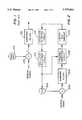
- FIG. 2is a schematic block diagram for circuitry of a preferred embodiment of the present invention.
- FIG. 3is a circuit diagram showing a preferred embodiment of the distortion detection circuit shown schematically in FIG. 2;
- FIG. 4is a block schematic diagram for circuitry of another embodiment of the invention.
- FIG. 2A schematic block diagram showing a preferred circuit design in accordance with the present invention is provided in FIG. 2.
- an RF signalis received by the receiver.
- the RF signalis downconverted to an IF signal using a mixer 202.
- the mixer 202receives a local oscillator (LO) signal from a variable conversion frequency signal element such as a VCO 204.
- An IF signalis output from the mixer 202 to a bandpass filter 206.
- the bandpass filter 206suppresses noise and out-of-band signals from the IF signal.
- the function and operation of the bandpass filter 206is similar to that of the bandpass filter 106 of FIG. 1.
- the output of the bandpass filter 206is input to a frequency correction circuit 208.
- the frequency correction circuit 208removes frequency offset introduced by error voltage control adjustments, discussed below, to the VCO 204. While a variety of circuits may be used to implement the frequency correction circuit 208, in a preferred embodiment, the frequency correction circuit 208 is implemented using a simple analog or digital servo loop.
- the output from the frequency correction circuit 208can be sinusoidal. Such a sinusoidal output is converted to a digital signal and sampled. Conversion to a digital signal and sampling is, in one embodiment, accomplished utilizing a limiter and sampler circuit 210. While sampling in the limiter and sampler circuit 210 can be accomplished utilizing a variety of techniques, in a preferred embodiment, sampling is conducted in a manner designed to provide optimum sampling time. In a preferred embodiment, optimum sampling time is achieved by centering between zero crossings of the signal output by the frequency correction circuit 208.
- the sinusoidal output from the frequency correction circuit 208is converted to a digital signal by the limiter and sampler circuit 210.
- the limiter and sampler circuit 210in a preferred embodiment, is constructed to allow digital conversion and to achieve optimum sampling time through inclusion of a limiter. A variety of designs will be evident to those of ordinary skill in the art for the implementation of the limiter in the limiter and sampler circuit 210.
- the limiterpreferably acts to determine the zero crossings in the signal and to convert the sinusoidal signal to a digital signal. In a preferred embodiment, these actions are accomplished in the limiter through including a comparator that forms a zero crossing detector and a D-type flip-flop.
- the output of the limiter and sampler circuit 210is input to a distortion detection circuit 212.
- the distortion detection circuit 212estimates the degree of distortion in an incoming signal based on an analysis of the digital data recovered from the received signal. If the input signal is modulated using minimum shift keying (MSK) with Gaussian filtering, the distortion can be estimated as a function of the sign of the digital data. Although MSK modulation is preferred, frequency shift keying (FSK) modulation may also be utilized and distortion can also be estimated as a function of the sign of the data.
- the distortion detection circuit 212estimates the distortion from the deviation error recovered from the output of bandpass filter 206.
- the distortion detection circuit 212provides a signal including positive frequency shift errors determined from digital ones identified from the bandpass filter output signal and negative frequency shift error values determined from digital zeros identified from the bandpass filter output.
- the signal output by the distortion detection circuit 212is converted to an analog signal by an oscillator adjustment circuit 214 to provide a voltage adjustment signal to the VCO 204 and frequency correction circuit 208.
- an oscillator adjustment circuit 214is an infinite impulse response filter.
- An infinite impulse response filterfunctions to provide the time integral of the output signal from the distortion detection circuit 212 as the voltage adjustment signal.
- the oscillator adjustment circuit 214is particularly desirable for the oscillator adjustment circuit 214 to be a digital device, because with a digital device, receiver operation can be improved in battery powered devices.
- digital componentscan be utilized which enter a sleep mode upon receipt of a sleep mode signal when a receiver input signal is not received for a period of time. When the receiver input signal later changes, the sleep mode signal is disabled and the digital components powered down will then utilize a short time period to power back up.
- the sleep modeis useful in battery powered devices, such as pagers, because without components being continually powered up, batteries are not constantly drained.
- oscillator adjustment circuit 214With the oscillator adjustment circuit 214 responding to a sleep mode signal, its voltage control output signal state upon receiving a sleep mode signal can be remembered upon power up when the sleep mode signal is disabled. With the voltage adjustment output of an oscillator adjustment circuit 214 remembered from receipt of the sleep mode signal, the receiver can more rapidly return to a condition of maximum distortion elimination upon power up. Without remembering a previous state, upon power up from a sleep mode, recovery time for the oscillator adjustment circuit to return to a state of maximum distortion elimination is substantially increased.
- An example of an oscillator adjustment circuit 214 which is a digital componentis the infinite impulse response filter referred to above.
- FIG. 3is a circuit diagram showing a preferred design of the distortion detection circuit 212 which is shown schematically in FIG. 2.
- the distortion detection circuit 212includes a data detection circuit 302 which receives the output from the sampler and limiter circuit 210.
- the data detection circuit 302identifies logical zeros and ones in the incoming signal.
- the data detection circuit 302provides a 1's clock output 303 that indicates when logical ones are detected and a 0's clock output 305 that indicates when logical zeros are detected.
- the distortion detection circuit 212further includes a frequency discriminator 306 which receives the output from the sampler and limiter circuit 210.
- the frequency discriminator 306compares the frequency of an internal reference signal with the frequency of the RF signal from the frequency correction circuit.
- the output of the frequency discriminator 306is provided to samplers 310 and 320 to enable the samplers to provide a digital output word representing a sampled value at a specific time instant as determined by the data detection circuit.
- the 1's clock output 303is output to a sampler 310 to enable sampling of the output of the frequency discriminator 306 during receipt of digital ones.
- the 0's clock output 305is output to a sampler 320 to enable sampling of the output of the frequency discriminator 306 during receipt of digital zeros.
- the output of the sampler 310is compared with the nominal value for a one in the comparison circuit 312 in order to provide a ones frequency shift error value (a "ones error value”).
- the absolute value of the ones error value from the comparison circuit 312is provided by an absolute value circuit 314.
- the output of the sampler 320is compared with the nominal value for a zero in a comparison circuit 322 in order to provide a zeros frequency shift error value (a "zeros error value”).
- the absolute value of the zeros error value from the comparison circuit 322is provided by an absolute value circuit 324.
- a multiplier 316has a first input 307 for receiving the ones frequency shift error value from the absolute value circuit 314, and a second input 309 for receiving a control signal 311.
- a multiplier 326has a first input 313 for receiving the zeros frequency shift error value from the absolute value circuit 324 and a second input 315 for receiving the inverse of the control signal 311 from an inverter 330.
- the control signal 311is preferably provided by a voltage reference. However, other sources for the control signal 311 can be utilized. For example, the combined 1's and 0's clock outputs, 303 and 305, respectively, of the data detection circuit 302 can be utilized as the control signal 311. Outputs of multipliers 316 and 326 are added by an adder 340 to provide an error signal output of the distortion detection circuit 212.
- the error signal output of the adder 340thus contains positive values and/or negative values indicating the magnitude of frequency shift errors for digital ones and/or zeros, respectively, that are identified in the signal output by the filter 206 (FIG. 2).
- the output of the adder 340is coupled to the oscillator adjustment circuit 214.
- the oscillator adjustment circuitintegrates the output from the adder 340 and feeds back the integrated output to the VCO 204 and the frequency correction circuit 208.
- the feed back signalacts to adjust the center frequency of signals input to the filter 206 so that the average distortion for ones and zeros at the filter output is made equal. In this manner, the bandwidth of the received signal is "matched" with the bandwidth of the bandpass filter 206. As discussed above, such "matching" suppresses noise and eliminates out-of-band signals.
- estimation of distortionis accomplished in the distortion detection circuit 212 of FIG. 3 through the use of positive values and negative values of the magnitude of frequency shift errors for the digital ones and zeros, respectively.
- other means for estimating distortion using recovered digital datacan also be utilized.
- sign values for frequency shift errorscan be reversed, i.e., negative values and positive values corresponding to the magnitudes of frequency shift errors for digital ones and digital zeros, respectively.
- the negative value corresponding to the magnitude of frequency shift errors for a particular combination of zeros and onesmay be used as opposed to positive values corresponding to other combinations of zeros and ones.
- FIG. 3shows specific components for the distortion detection circuit 212
- other implementationsare possible and contemplated by the present invention.
- a variety of similar and equivalent circuitscan be designed and utilized in accordance with the invention.
- certain software and/or programmable implementationsare also contemplated.
- a digital signal processor (DSP) or microprocessorcan be substituted for the distortion detection circuit 212 and programmed to provide a function similar to the circuitry shown in FIG. 3 or equivalent circuits.
- the output from the bandpass filter 206is converted to a baseband signal and digitized using the limiter and sampler circuit 210.
- the limiter and sampler circuit 210it will be appreciated that a variety of other methods of converting the bandpass filter 206 output to a baseband signal and digitizing the signal can be utilized.
- FIG. 4is a schematic block diagram of another circuit design in accordance with the present invention.
- the circuit of FIG. 4enables in-phase (I) and quadrature (Q) demodulation.
- the limiter and sampler circuit 210(FIG. 2) is replaced with an I/Q demodulator 402, a low pass filter 404, and an analog to digital (A/D) convertor 406.
- the output from the bandpass filter 206is converted to a baseband signal through the I/Q demodulator 402.
- the I/Q demodulatorconverts the output of the bandpass filter 206 to a baseband signal using in-phase (I) and quadrature (Q) demodulation.
- the baseband signalis output from the I/Q demodulator 402 to the low pass filter 404.
- the low pass filter 404is output to the A/D convertor 406 which converts the baseband signal to a digital signal.
- the digital output from the A/D convertor 406is output to the distortion detection unit 212.
- the remaining components shown in FIG. 4are similar to those shown in FIG. 2, and are identified using similar reference numbers and operate as discussed previously with reference to FIG. 2.
Landscapes
- Engineering & Computer Science (AREA)
- Computer Networks & Wireless Communication (AREA)
- Signal Processing (AREA)
- Noise Elimination (AREA)
- Digital Transmission Methods That Use Modulated Carrier Waves (AREA)
- Superheterodyne Receivers (AREA)
Abstract
Description
Claims (23)
Priority Applications (6)
| Application Number | Priority Date | Filing Date | Title |
|---|---|---|---|
| US08/516,197US5757864A (en) | 1995-08-17 | 1995-08-17 | Receiver with filters offset correction |
| DE69630237TDE69630237T2 (en) | 1995-08-17 | 1996-07-29 | RECEIVER WITH CORRECTION OF FILTER SHIFTING |
| PCT/US1996/012445WO1997007618A1 (en) | 1995-08-17 | 1996-07-29 | Receiver with filter offset correction |
| AU66048/96AAU6604896A (en) | 1995-08-17 | 1996-07-29 | Receiver with filter offset correction |
| EP96925573AEP0883951B1 (en) | 1995-08-17 | 1996-07-29 | Receiver with filter offset correction |
| JP50930497AJP3756190B2 (en) | 1995-08-17 | 1996-07-29 | Receiver having filter offset correction function |
Applications Claiming Priority (1)
| Application Number | Priority Date | Filing Date | Title |
|---|---|---|---|
| US08/516,197US5757864A (en) | 1995-08-17 | 1995-08-17 | Receiver with filters offset correction |
Publications (1)
| Publication Number | Publication Date |
|---|---|
| US5757864Atrue US5757864A (en) | 1998-05-26 |
Family
ID=24054546
Family Applications (1)
| Application Number | Title | Priority Date | Filing Date |
|---|---|---|---|
| US08/516,197Expired - LifetimeUS5757864A (en) | 1995-08-17 | 1995-08-17 | Receiver with filters offset correction |
Country Status (6)
| Country | Link |
|---|---|
| US (1) | US5757864A (en) |
| EP (1) | EP0883951B1 (en) |
| JP (1) | JP3756190B2 (en) |
| AU (1) | AU6604896A (en) |
| DE (1) | DE69630237T2 (en) |
| WO (1) | WO1997007618A1 (en) |
Cited By (27)
| Publication number | Priority date | Publication date | Assignee | Title |
|---|---|---|---|---|
| US6226505B1 (en)* | 1996-11-20 | 2001-05-01 | Nec Corporation | Automatic frequency correction apparatus and method for radio calling system |
| US6385442B1 (en)* | 1998-03-04 | 2002-05-07 | Symbol Technologies, Inc. | Multiphase receiver and oscillator |
| US6631174B1 (en)* | 1999-06-09 | 2003-10-07 | Mitsubishi Denki Kabushiki Kaisha | Automatic frequency control apparatus |
| US6636731B1 (en)* | 1999-09-14 | 2003-10-21 | Koninklijke Philips Electronics N.V. | Demodulation method preserving a high spectral purity |
| US20040124335A1 (en)* | 2002-12-27 | 2004-07-01 | Cicchiello James M. | Real-time correction of phase distortion |
| US20050009478A1 (en)* | 2000-07-25 | 2005-01-13 | Chandra Mohan | In-band-on-channel broadcast system for digital data |
| US6874115B1 (en)* | 2000-08-04 | 2005-03-29 | Agere Systems Inc. | Multi-mode decoding for digital audio broadcasting and other applications |
| US20050242860A1 (en)* | 2004-04-30 | 2005-11-03 | Weijie Yun | FFT-based multichannel video receiver |
| US20060198474A1 (en)* | 1999-04-16 | 2006-09-07 | Parker Vision, Inc. | Method and system for down-converting and electromagnetic signal, and transforms for same |
| US20070014335A1 (en)* | 2005-07-18 | 2007-01-18 | Callaway Edgar H | Method and apparatus for reducing power consumption within a wireless receiver |
| US20070041435A1 (en)* | 2002-07-18 | 2007-02-22 | Parkervision, Inc. | Networking methods and systems |
| US20070293182A1 (en)* | 2000-04-14 | 2007-12-20 | Parkervision, Inc. | Apparatus, system, and method for down converting and up converting electromagnetic signals |
| US20080182544A1 (en)* | 1998-10-21 | 2008-07-31 | Parkervision, Inc. | Methods and Systems for Down-Converting a Signal Using a Complementary Transistor Structure |
| US20080270170A1 (en)* | 2002-07-18 | 2008-10-30 | Parkervision, Inc. | Networking Methods and Systems |
| US20090022245A1 (en)* | 2006-05-24 | 2009-01-22 | General Dynamics Advanced Information Systems | Low latency analog QAM coherent demodulation algorithm |
| US7826817B2 (en) | 1998-10-21 | 2010-11-02 | Parker Vision, Inc. | Applications of universal frequency translation |
| US7865177B2 (en) | 1998-10-21 | 2011-01-04 | Parkervision, Inc. | Method and system for down-converting an electromagnetic signal, and transforms for same, and aperture relationships |
| US7894789B2 (en) | 1999-04-16 | 2011-02-22 | Parkervision, Inc. | Down-conversion of an electromagnetic signal with feedback control |
| US7929638B2 (en) | 1999-04-16 | 2011-04-19 | Parkervision, Inc. | Wireless local area network (WLAN) using universal frequency translation technology including multi-phase embodiments |
| US7991815B2 (en) | 2000-11-14 | 2011-08-02 | Parkervision, Inc. | Methods, systems, and computer program products for parallel correlation and applications thereof |
| US8019291B2 (en) | 1998-10-21 | 2011-09-13 | Parkervision, Inc. | Method and system for frequency down-conversion and frequency up-conversion |
| US8036304B2 (en) | 1999-04-16 | 2011-10-11 | Parkervision, Inc. | Apparatus and method of differential IQ frequency up-conversion |
| US8077797B2 (en) | 1999-04-16 | 2011-12-13 | Parkervision, Inc. | Method, system, and apparatus for balanced frequency up-conversion of a baseband signal |
| US8233855B2 (en) | 1998-10-21 | 2012-07-31 | Parkervision, Inc. | Up-conversion based on gated information signal |
| US8295406B1 (en)* | 1999-08-04 | 2012-10-23 | Parkervision, Inc. | Universal platform module for a plurality of communication protocols |
| US8446994B2 (en) | 2001-11-09 | 2013-05-21 | Parkervision, Inc. | Gain control in a communication channel |
| US20150137883A1 (en)* | 2013-11-19 | 2015-05-21 | Qualcomm Incorporated | Adaptive fm demodulator supporting multiple modes |
Families Citing this family (5)
| Publication number | Priority date | Publication date | Assignee | Title |
|---|---|---|---|---|
| FR2792140A1 (en)* | 1999-04-07 | 2000-10-13 | Koninkl Philips Electronics Nv | FREQUENCY CORRECTION TO RECEPTION IN A PACKET TRANSMISSION SYSTEM |
| RU2157050C1 (en)* | 1999-07-29 | 2000-09-27 | Гармонов Александр Васильевич | Method for measuring frequency and device which implements said method |
| RU2259011C1 (en)* | 2004-06-28 | 2005-08-20 | Федеральное государственное унитарное предприятие "Воронежский научно-исследовательский институт связи" | Device for suppressing narrow-band interferences |
| CN103581083B (en)* | 2013-11-11 | 2016-06-08 | 浙江大学 | A kind of highly reliable and low-cost observing and controlling answering machine carrier tracking loop and method thereof |
| JP6922801B2 (en)* | 2018-03-20 | 2021-08-18 | 株式会社Jvcケンウッド | Receiver, receiving method |
Citations (14)
| Publication number | Priority date | Publication date | Assignee | Title |
|---|---|---|---|---|
| US3657661A (en)* | 1970-06-16 | 1972-04-18 | Itt | Fm demodulator system |
| US4078212A (en)* | 1976-02-27 | 1978-03-07 | Rca Corporation | Dual mode frequency synthesizer for a television tuning apparatus |
| US4237556A (en)* | 1978-03-06 | 1980-12-02 | Trio Kabushiki Kaisha | Superheterodyne receiver having distortion reducing circuitry |
| US4466128A (en)* | 1981-01-15 | 1984-08-14 | Texas Instruments Incorporated | Automatically centered pulsed FM receiver |
| US4528698A (en)* | 1983-12-22 | 1985-07-09 | Motorola, Inc. | Tuning system for RF receiver |
| US4599732A (en)* | 1984-04-17 | 1986-07-08 | Harris Corporation | Technique for acquiring timing and frequency synchronization for modem utilizing known (non-data) symbols as part of their normal transmitted data format |
| US4903332A (en)* | 1984-10-16 | 1990-02-20 | H.U.C. Elecktronik Gmbh | Filter and demodulation circuit for filtering an intermediate frequency modulated signal carrying a modulation signal |
| US5012490A (en)* | 1989-12-26 | 1991-04-30 | At&T Bell Laboratories | Varying bandwidth digital signal detector |
| US5065453A (en)* | 1989-03-20 | 1991-11-12 | General Electric Company | Electrically-tunable bandpass filter |
| US5101509A (en)* | 1990-09-14 | 1992-03-31 | Ford Motor Company | Rf filter alignment using digital processor clock |
| US5222106A (en)* | 1990-02-07 | 1993-06-22 | Kokusai Denshin Denwa Kabushiki Kaisha | Interference detection and reduction |
| US5404589A (en)* | 1992-06-26 | 1995-04-04 | U.S. Philips Corporation | FM receiver with dynamic intermediate frequency (IF) filter tuning |
| US5418815A (en)* | 1992-06-12 | 1995-05-23 | Kabushiki Kaisha Toshiba | Receiver adaptively operable for multiple signal transmission systems |
| US5487186A (en)* | 1993-06-28 | 1996-01-23 | Hitachi America, Ltd. | Automatic frequency control using split-band signal strength measurements |
Family Cites Families (3)
| Publication number | Priority date | Publication date | Assignee | Title |
|---|---|---|---|---|
| US5291206A (en)* | 1967-09-14 | 1994-03-01 | Hughes Missile Systems Company | Multiple target discrimination system |
| CH553514A (en)* | 1972-12-27 | 1974-08-30 | Bbc Brown Boveri & Cie | TRAIL RECEIVER. |
| JPS61147315A (en)* | 1984-12-20 | 1986-07-05 | Toshiba Corp | Loop compensation filter |
- 1995
- 1995-08-17USUS08/516,197patent/US5757864A/ennot_activeExpired - Lifetime
- 1996
- 1996-07-29EPEP96925573Apatent/EP0883951B1/ennot_activeExpired - Lifetime
- 1996-07-29WOPCT/US1996/012445patent/WO1997007618A1/enactiveIP Right Grant
- 1996-07-29DEDE69630237Tpatent/DE69630237T2/ennot_activeExpired - Lifetime
- 1996-07-29AUAU66048/96Apatent/AU6604896A/ennot_activeAbandoned
- 1996-07-29JPJP50930497Apatent/JP3756190B2/ennot_activeExpired - Lifetime
Patent Citations (14)
| Publication number | Priority date | Publication date | Assignee | Title |
|---|---|---|---|---|
| US3657661A (en)* | 1970-06-16 | 1972-04-18 | Itt | Fm demodulator system |
| US4078212A (en)* | 1976-02-27 | 1978-03-07 | Rca Corporation | Dual mode frequency synthesizer for a television tuning apparatus |
| US4237556A (en)* | 1978-03-06 | 1980-12-02 | Trio Kabushiki Kaisha | Superheterodyne receiver having distortion reducing circuitry |
| US4466128A (en)* | 1981-01-15 | 1984-08-14 | Texas Instruments Incorporated | Automatically centered pulsed FM receiver |
| US4528698A (en)* | 1983-12-22 | 1985-07-09 | Motorola, Inc. | Tuning system for RF receiver |
| US4599732A (en)* | 1984-04-17 | 1986-07-08 | Harris Corporation | Technique for acquiring timing and frequency synchronization for modem utilizing known (non-data) symbols as part of their normal transmitted data format |
| US4903332A (en)* | 1984-10-16 | 1990-02-20 | H.U.C. Elecktronik Gmbh | Filter and demodulation circuit for filtering an intermediate frequency modulated signal carrying a modulation signal |
| US5065453A (en)* | 1989-03-20 | 1991-11-12 | General Electric Company | Electrically-tunable bandpass filter |
| US5012490A (en)* | 1989-12-26 | 1991-04-30 | At&T Bell Laboratories | Varying bandwidth digital signal detector |
| US5222106A (en)* | 1990-02-07 | 1993-06-22 | Kokusai Denshin Denwa Kabushiki Kaisha | Interference detection and reduction |
| US5101509A (en)* | 1990-09-14 | 1992-03-31 | Ford Motor Company | Rf filter alignment using digital processor clock |
| US5418815A (en)* | 1992-06-12 | 1995-05-23 | Kabushiki Kaisha Toshiba | Receiver adaptively operable for multiple signal transmission systems |
| US5404589A (en)* | 1992-06-26 | 1995-04-04 | U.S. Philips Corporation | FM receiver with dynamic intermediate frequency (IF) filter tuning |
| US5487186A (en)* | 1993-06-28 | 1996-01-23 | Hitachi America, Ltd. | Automatic frequency control using split-band signal strength measurements |
Non-Patent Citations (2)
| Title |
|---|
| Panter, Philip F., Ph.D., Modulation, Noise, And Spectral Analysis, 1965, McGraw Hill Book Company, Chap. 16, Threshold Extension in Frequency Modulation Receivers, pp. 478 483.* |
| Panter, Philip F., Ph.D., Modulation, Noise, And Spectral Analysis, 1965, McGraw-Hill Book Company, Chap. 16, Threshold Extension in Frequency Modulation Receivers, pp. 478-483. |
Cited By (48)
| Publication number | Priority date | Publication date | Assignee | Title |
|---|---|---|---|---|
| US6226505B1 (en)* | 1996-11-20 | 2001-05-01 | Nec Corporation | Automatic frequency correction apparatus and method for radio calling system |
| US6385442B1 (en)* | 1998-03-04 | 2002-05-07 | Symbol Technologies, Inc. | Multiphase receiver and oscillator |
| US8190108B2 (en) | 1998-10-21 | 2012-05-29 | Parkervision, Inc. | Method and system for frequency up-conversion |
| US8233855B2 (en) | 1998-10-21 | 2012-07-31 | Parkervision, Inc. | Up-conversion based on gated information signal |
| US8340618B2 (en) | 1998-10-21 | 2012-12-25 | Parkervision, Inc. | Method and system for down-converting an electromagnetic signal, and transforms for same, and aperture relationships |
| US8190116B2 (en) | 1998-10-21 | 2012-05-29 | Parker Vision, Inc. | Methods and systems for down-converting a signal using a complementary transistor structure |
| US20080182544A1 (en)* | 1998-10-21 | 2008-07-31 | Parkervision, Inc. | Methods and Systems for Down-Converting a Signal Using a Complementary Transistor Structure |
| US8160534B2 (en) | 1998-10-21 | 2012-04-17 | Parkervision, Inc. | Applications of universal frequency translation |
| US8019291B2 (en) | 1998-10-21 | 2011-09-13 | Parkervision, Inc. | Method and system for frequency down-conversion and frequency up-conversion |
| US7937059B2 (en) | 1998-10-21 | 2011-05-03 | Parkervision, Inc. | Converting an electromagnetic signal via sub-sampling |
| US7936022B2 (en) | 1998-10-21 | 2011-05-03 | Parkervision, Inc. | Method and circuit for down-converting a signal |
| US7865177B2 (en) | 1998-10-21 | 2011-01-04 | Parkervision, Inc. | Method and system for down-converting an electromagnetic signal, and transforms for same, and aperture relationships |
| US7826817B2 (en) | 1998-10-21 | 2010-11-02 | Parker Vision, Inc. | Applications of universal frequency translation |
| US20080272441A1 (en)* | 1998-10-21 | 2008-11-06 | Parkervision, Inc. | Method and circuit for down-converting a signal |
| US8223898B2 (en) | 1999-04-16 | 2012-07-17 | Parkervision, Inc. | Method and system for down-converting an electromagnetic signal, and transforms for same |
| US20060198474A1 (en)* | 1999-04-16 | 2006-09-07 | Parker Vision, Inc. | Method and system for down-converting and electromagnetic signal, and transforms for same |
| US8594228B2 (en) | 1999-04-16 | 2013-11-26 | Parkervision, Inc. | Apparatus and method of differential IQ frequency up-conversion |
| US7724845B2 (en) | 1999-04-16 | 2010-05-25 | Parkervision, Inc. | Method and system for down-converting and electromagnetic signal, and transforms for same |
| US8229023B2 (en) | 1999-04-16 | 2012-07-24 | Parkervision, Inc. | Wireless local area network (WLAN) using universal frequency translation technology including multi-phase embodiments |
| US8224281B2 (en) | 1999-04-16 | 2012-07-17 | Parkervision, Inc. | Down-conversion of an electromagnetic signal with feedback control |
| US8077797B2 (en) | 1999-04-16 | 2011-12-13 | Parkervision, Inc. | Method, system, and apparatus for balanced frequency up-conversion of a baseband signal |
| US8036304B2 (en) | 1999-04-16 | 2011-10-11 | Parkervision, Inc. | Apparatus and method of differential IQ frequency up-conversion |
| US7894789B2 (en) | 1999-04-16 | 2011-02-22 | Parkervision, Inc. | Down-conversion of an electromagnetic signal with feedback control |
| US7929638B2 (en) | 1999-04-16 | 2011-04-19 | Parkervision, Inc. | Wireless local area network (WLAN) using universal frequency translation technology including multi-phase embodiments |
| US6631174B1 (en)* | 1999-06-09 | 2003-10-07 | Mitsubishi Denki Kabushiki Kaisha | Automatic frequency control apparatus |
| US8295406B1 (en)* | 1999-08-04 | 2012-10-23 | Parkervision, Inc. | Universal platform module for a plurality of communication protocols |
| US6636731B1 (en)* | 1999-09-14 | 2003-10-21 | Koninklijke Philips Electronics N.V. | Demodulation method preserving a high spectral purity |
| US8295800B2 (en) | 2000-04-14 | 2012-10-23 | Parkervision, Inc. | Apparatus and method for down-converting electromagnetic signals by controlled charging and discharging of a capacitor |
| US20070293182A1 (en)* | 2000-04-14 | 2007-12-20 | Parkervision, Inc. | Apparatus, system, and method for down converting and up converting electromagnetic signals |
| US7822401B2 (en) | 2000-04-14 | 2010-10-26 | Parkervision, Inc. | Apparatus and method for down-converting electromagnetic signals by controlled charging and discharging of a capacitor |
| US20050009478A1 (en)* | 2000-07-25 | 2005-01-13 | Chandra Mohan | In-band-on-channel broadcast system for digital data |
| US6874115B1 (en)* | 2000-08-04 | 2005-03-29 | Agere Systems Inc. | Multi-mode decoding for digital audio broadcasting and other applications |
| US7991815B2 (en) | 2000-11-14 | 2011-08-02 | Parkervision, Inc. | Methods, systems, and computer program products for parallel correlation and applications thereof |
| US8446994B2 (en) | 2001-11-09 | 2013-05-21 | Parkervision, Inc. | Gain control in a communication channel |
| US8160196B2 (en) | 2002-07-18 | 2012-04-17 | Parkervision, Inc. | Networking methods and systems |
| US8407061B2 (en) | 2002-07-18 | 2013-03-26 | Parkervision, Inc. | Networking methods and systems |
| US20080270170A1 (en)* | 2002-07-18 | 2008-10-30 | Parkervision, Inc. | Networking Methods and Systems |
| US20070041435A1 (en)* | 2002-07-18 | 2007-02-22 | Parkervision, Inc. | Networking methods and systems |
| US20040124335A1 (en)* | 2002-12-27 | 2004-07-01 | Cicchiello James M. | Real-time correction of phase distortion |
| US7146060B2 (en)* | 2002-12-27 | 2006-12-05 | Cicchiello James M | Real-time correction of phase distortion |
| US20080260044A1 (en)* | 2004-04-30 | 2008-10-23 | Weijie Yun | Fft-based multichannel video receiver |
| US20050242860A1 (en)* | 2004-04-30 | 2005-11-03 | Weijie Yun | FFT-based multichannel video receiver |
| US20070014335A1 (en)* | 2005-07-18 | 2007-01-18 | Callaway Edgar H | Method and apparatus for reducing power consumption within a wireless receiver |
| US7339976B2 (en)* | 2005-07-18 | 2008-03-04 | Motorola, Inc. | Method and apparatus for reducing power consumption within a wireless receiver |
| US20090022245A1 (en)* | 2006-05-24 | 2009-01-22 | General Dynamics Advanced Information Systems | Low latency analog QAM coherent demodulation algorithm |
| US7801250B2 (en) | 2006-05-24 | 2010-09-21 | General Dynamics Advanced Information Systems, Inc. | Low latency analog QAM coherent demodulation algorithm |
| US20150137883A1 (en)* | 2013-11-19 | 2015-05-21 | Qualcomm Incorporated | Adaptive fm demodulator supporting multiple modes |
| US9143087B2 (en)* | 2013-11-19 | 2015-09-22 | Qualcomm Incorporated | Adaptive FM demodulator supporting multiple modes |
Also Published As
| Publication number | Publication date |
|---|---|
| EP0883951A4 (en) | 2001-12-19 |
| JP3756190B2 (en) | 2006-03-15 |
| EP0883951A1 (en) | 1998-12-16 |
| EP0883951B1 (en) | 2003-10-01 |
| DE69630237D1 (en) | 2003-11-06 |
| DE69630237T2 (en) | 2004-08-05 |
| WO1997007618A1 (en) | 1997-02-27 |
| AU6604896A (en) | 1997-03-12 |
| JPH11511311A (en) | 1999-09-28 |
Similar Documents
| Publication | Publication Date | Title |
|---|---|---|
| US5757864A (en) | Receiver with filters offset correction | |
| US7200188B2 (en) | Method and apparatus for frequency offset compensation | |
| US8498601B2 (en) | Polar receiver using injection-locking technique | |
| US5425057A (en) | Phase demodulation method and apparatus using asynchronous sampling pulses | |
| US8442474B2 (en) | Method and apparatus for imbalance-free FM demodulation in direct conversion radio receivers | |
| US20070047737A1 (en) | Fm stereo decoder incorporating costas loop pilot to stereo component phase correction | |
| EP1058396A1 (en) | Very low IF receiver circuit and method | |
| KR980007647A (en) | Digital Demodulation Circuit and Method of High Resolution Television Receiver | |
| US6868129B2 (en) | Demodulator for a radio receiver and method of operation | |
| KR100406224B1 (en) | Frequency modulation signaling inquiry and communication terminal equipment employing it | |
| CN111492533B (en) | Phase synchronization device | |
| US20070127611A1 (en) | Non-coherent synchronous direct-conversion receiving apparatus for compensating frequency offset | |
| EP0373517B1 (en) | Digital automatic frequency control on pure sine waves | |
| US7751303B2 (en) | Demodulation circuit for use in receiver using if directing sampling scheme | |
| JP2959498B2 (en) | Automatic frequency control circuit | |
| US20020176517A1 (en) | Receiving device for angle-modulated signals | |
| US7010063B2 (en) | Receiver circuit and method of processing a received signal | |
| US6914946B1 (en) | Digitally-implemented demodulator | |
| KR100245330B1 (en) | Phase and frequency detector of digital communication system | |
| KR20010042028A (en) | Demodulator circuits | |
| EP1058378B1 (en) | Multiplier for multiplying complex signals | |
| JP2002353835A (en) | Receiver | |
| KR100309097B1 (en) | Method and apparatus of fine tuning for television receiver and method and apparatus of matching vsb signal | |
| EP1150436B1 (en) | Method and arrangement for receiving a frequency modulated signal | |
| CN114900405A (en) | A Soc-based Acars Signal Demodulation Method |
Legal Events
| Date | Code | Title | Description |
|---|---|---|---|
| AS | Assignment | Owner name:PACIFIC COMMUNICATIONS SCIENCES, INC., CALIFORNIA Free format text:ASSIGNMENT OF ASSIGNORS INTEREST;ASSIGNORS:PETRANOVICH, JAMES E.;LIPOWSKI, JOSEPH T.;REEL/FRAME:007733/0287;SIGNING DATES FROM 19951011 TO 19951016 Owner name:PACIFIC COMMUNICATIONS SCIENCES, INC., CALIFORNIA Free format text:ASSIGNMENT OF ASSIGNORS INTEREST;ASSIGNORS:PETRANOVICH, JAMES E.;LIPOWSKI, JOSEPH T.;REEL/FRAME:007733/0292;SIGNING DATES FROM 19951011 TO 19951016 | |
| AS | Assignment | Owner name:ROCKWELL SEMICONDUCTOR SYSTEMS, INC., CALIFORNIA Free format text:ASSIGNMENT OF ASSIGNORS INTEREST;ASSIGNOR:PACIFIC COMMUNICATION SCIENCES, INC.;REEL/FRAME:008470/0140 Effective date:19970128 | |
| STCF | Information on status: patent grant | Free format text:PATENTED CASE | |
| AS | Assignment | Owner name:CREDIT SUISSE FIRST BOSTON, NEW YORK Free format text:SECURITY INTEREST;ASSIGNORS:CONEXANT SYSTEMS, INC.;BROOKTREE CORPORATION;BROOKTREE WORLDWIDE SALES CORPORATION;AND OTHERS;REEL/FRAME:009719/0537 Effective date:19981221 | |
| AS | Assignment | Owner name:CONEXANT SYSTEMS, INC., CALIFORNIA Free format text:CHANGE OF NAME;ASSIGNOR:ROCKWELL SEMICONDUCTOR SYSTEMS, INC.;REEL/FRAME:010238/0537 Effective date:19981014 | |
| AS | Assignment | Owner name:CONEXANT SYSTEMS, INC., CALIFORNIA Free format text:ASSIGNMENT OF ASSIGNORS INTEREST;ASSIGNOR:ROCKWELL SCIENCE CENTER, LLC;REEL/FRAME:010415/0761 Effective date:19981210 | |
| FEPP | Fee payment procedure | Free format text:PAYOR NUMBER ASSIGNED (ORIGINAL EVENT CODE: ASPN); ENTITY STATUS OF PATENT OWNER: LARGE ENTITY | |
| AS | Assignment | Owner name:CONEXANT SYSTEMS, INC., CALIFORNIA Free format text:RELEASE OF SECURITY INTEREST;ASSIGNOR:CREDIT SUISSE FIRST BOSTON;REEL/FRAME:012252/0413 Effective date:20011018 Owner name:BROOKTREE CORPORATION, CALIFORNIA Free format text:RELEASE OF SECURITY INTEREST;ASSIGNOR:CREDIT SUISSE FIRST BOSTON;REEL/FRAME:012252/0413 Effective date:20011018 Owner name:BROOKTREE WORLDWIDE SALES CORPORATION, CALIFORNIA Free format text:RELEASE OF SECURITY INTEREST;ASSIGNOR:CREDIT SUISSE FIRST BOSTON;REEL/FRAME:012252/0413 Effective date:20011018 Owner name:CONEXANT SYSTEMS WORLDWIDE, INC., CALIFORNIA Free format text:RELEASE OF SECURITY INTEREST;ASSIGNOR:CREDIT SUISSE FIRST BOSTON;REEL/FRAME:012252/0413 Effective date:20011018 | |
| FPAY | Fee payment | Year of fee payment:4 | |
| AS | Assignment | Owner name:ALPHA INDUSTRIES, INC., CALIFORNIA Free format text:MERGER;ASSIGNOR:WASHINGTON SUB, INC.;REEL/FRAME:013258/0498 Effective date:20020625 Owner name:WASHINGTON SUB, INC., CALIFORNIA Free format text:ASSIGNMENT OF ASSIGNORS INTEREST;ASSIGNOR:CONEXANT SYSTEMS, INC.;REEL/FRAME:013258/0176 Effective date:20020625 | |
| AS | Assignment | Owner name:SKYWORKS SOLUTIONS, INC., CALIFORNIA Free format text:MERGER;ASSIGNOR:ALPHA INDUSTRIES, INC.;REEL/FRAME:013280/0206 Effective date:20020625 | |
| AS | Assignment | Owner name:CONEXANT SYSTEMS, INC., CALIFORNIA Free format text:SECURITY INTEREST;ASSIGNOR:ALPHA INDUSTRIES, INC.;REEL/FRAME:013240/0860 Effective date:20020625 | |
| AS | Assignment | Owner name:CONEXANT SYSTEMS, INC., CALIFORNIA Free format text:ASSIGNMENT OF ASSIGNORS INTEREST;ASSIGNOR:ROCKWELL SEMICONDUCTOR SYSTEMS, INC.;REEL/FRAME:014268/0216 Effective date:19981014 | |
| AS | Assignment | Owner name:ALPHA INDUSTRIES, INC., MASSACHUSETTS Free format text:RELEASE AND RECONVEYANCE/SECURITY INTEREST;ASSIGNOR:CONEXANT SYSTEMS, INC.;REEL/FRAME:014580/0880 Effective date:20030307 | |
| FPAY | Fee payment | Year of fee payment:8 | |
| FPAY | Fee payment | Year of fee payment:12 |