US5754475A - Bit line discharge method for reading a multiple bits-per-cell flash EEPROM - Google Patents
Bit line discharge method for reading a multiple bits-per-cell flash EEPROMDownload PDFInfo
- Publication number
- US5754475A US5754475AUS08/884,547US88454797AUS5754475AUS 5754475 AUS5754475 AUS 5754475AUS 88454797 AUS88454797 AUS 88454797AUS 5754475 AUS5754475 AUS 5754475A
- Authority
- US
- United States
- Prior art keywords
- memory core
- cells
- array
- memory
- cell
- Prior art date
- Legal status (The legal status is an assumption and is not a legal conclusion. Google has not performed a legal analysis and makes no representation as to the accuracy of the status listed.)
- Expired - Lifetime
Links
- 238000000034methodMethods0.000titleclaimsdescription14
- 230000015654memoryEffects0.000claimsabstractdescription159
- 238000007667floatingMethods0.000claimsdescription14
- 238000003860storageMethods0.000claimsdescription5
- 230000004044responseEffects0.000claimsdescription4
- 238000007599dischargingMethods0.000claims1
- 238000009826distributionMethods0.000description10
- 239000004065semiconductorSubstances0.000description9
- 239000000758substrateSubstances0.000description7
- 230000001419dependent effectEffects0.000description5
- 238000010586diagramMethods0.000description4
- 239000011159matrix materialSubstances0.000description3
- 230000006870functionEffects0.000description2
- 239000002784hot electronSubstances0.000description2
- 238000012986modificationMethods0.000description2
- 230000004048modificationEffects0.000description2
- 230000008569processEffects0.000description2
- LZIAMMQBHJIZAG-UHFFFAOYSA-N2-[di(propan-2-yl)amino]ethyl carbamimidothioateChemical compoundCC(C)N(C(C)C)CCSC(N)=NLZIAMMQBHJIZAG-UHFFFAOYSA-N0.000description1
- 230000005689Fowler Nordheim tunnelingEffects0.000description1
- 108010075750P-Type Calcium ChannelsProteins0.000description1
- 238000003491arrayMethods0.000description1
- 238000010276constructionMethods0.000description1
- 230000001351cycling effectEffects0.000description1
- 230000000694effectsEffects0.000description1
- 230000005684electric fieldEffects0.000description1
- 238000005516engineering processMethods0.000description1
- 230000006872improvementEffects0.000description1
- 238000002347injectionMethods0.000description1
- 239000007924injectionSubstances0.000description1
- 238000004519manufacturing processMethods0.000description1
- 239000000463materialSubstances0.000description1
- 238000000926separation methodMethods0.000description1
Images


Classifications
- G—PHYSICS
- G11—INFORMATION STORAGE
- G11C—STATIC STORES
- G11C11/00—Digital stores characterised by the use of particular electric or magnetic storage elements; Storage elements therefor
- G11C11/56—Digital stores characterised by the use of particular electric or magnetic storage elements; Storage elements therefor using storage elements with more than two stable states represented by steps, e.g. of voltage, current, phase, frequency
- G11C11/5621—Digital stores characterised by the use of particular electric or magnetic storage elements; Storage elements therefor using storage elements with more than two stable states represented by steps, e.g. of voltage, current, phase, frequency using charge storage in a floating gate
- G11C11/5628—Programming or writing circuits; Data input circuits
- G—PHYSICS
- G11—INFORMATION STORAGE
- G11C—STATIC STORES
- G11C11/00—Digital stores characterised by the use of particular electric or magnetic storage elements; Storage elements therefor
- G11C11/56—Digital stores characterised by the use of particular electric or magnetic storage elements; Storage elements therefor using storage elements with more than two stable states represented by steps, e.g. of voltage, current, phase, frequency
- G11C11/5621—Digital stores characterised by the use of particular electric or magnetic storage elements; Storage elements therefor using storage elements with more than two stable states represented by steps, e.g. of voltage, current, phase, frequency using charge storage in a floating gate
- G11C11/5642—Sensing or reading circuits; Data output circuits
- G—PHYSICS
- G11—INFORMATION STORAGE
- G11C—STATIC STORES
- G11C2211/00—Indexing scheme relating to digital stores characterized by the use of particular electric or magnetic storage elements; Storage elements therefor
- G11C2211/56—Indexing scheme relating to G11C11/56 and sub-groups for features not covered by these groups
- G11C2211/562—Multilevel memory programming aspects
- G11C2211/5622—Concurrent multilevel programming of more than one cell
- G—PHYSICS
- G11—INFORMATION STORAGE
- G11C—STATIC STORES
- G11C2211/00—Indexing scheme relating to digital stores characterized by the use of particular electric or magnetic storage elements; Storage elements therefor
- G11C2211/56—Indexing scheme relating to G11C11/56 and sub-groups for features not covered by these groups
- G11C2211/563—Multilevel memory reading aspects
- G11C2211/5634—Reference cells
- G—PHYSICS
- G11—INFORMATION STORAGE
- G11C—STATIC STORES
- G11C2211/00—Indexing scheme relating to digital stores characterized by the use of particular electric or magnetic storage elements; Storage elements therefor
- G11C2211/56—Indexing scheme relating to G11C11/56 and sub-groups for features not covered by these groups
- G11C2211/564—Miscellaneous aspects
- G11C2211/5642—Multilevel memory with buffers, latches, registers at input or output
Definitions
- This inventionrelates generally to floating gate memory devices such as an array of flash electrically, erasable programmable read-only memory (EEPROM) cells. More particularly, it relates to a semiconductor integrated circuit memory device having an improved reading scheme for performing a read operation in an array of two bits-per-cell flash EEPROM memory cells so as to render enhanced efficiency.
- EEPROMerasable programmable read-only memory
- Flash EPROMelectrically erasable EPROMs/EEPROMs
- a plurality of one-transistor flash EEPROM core cellsmay be formed on a semiconductor substrate in which each cell is comprised of a P-type conductivity substrate, an N-type conductivity source region formed integrally with the substrate, and an N-type conductivity drain region also formed integrally within the substrate.
- a floating gateis separated from the substrate by a thin dielectric layer.
- a second dielectric layerseparates a control gate from the floating gate.
- a P-type channel region in the substrateseparates the source and drain regions.
- the drain region and the control gateare raised to predetermined potentials above the potential applied to the source region.
- the drain regionhas applied thereto a voltage V D of approximately +5.5 volts with the control gate V G having a voltage of approximately +12 volts applied thereto.
- V Dvoltage of approximately +5.5 volts
- V Gvoltage of approximately +12 volts applied thereto.
- a positive potentiale.g., +5 volts
- the control gateis at a negative potential (e.g., -8 volts), and the drain region is allowed to float.
- a strong electric fielddevelops between the floating gate and the source region, and a negative charge is extracted from the floating gate to the source region by way of Fowler-Nordheim tunneling.
- the magnitude of the read currentis measured.
- the source regionis held at a ground potential (0 volts) and the control gate is held at a potential of about +5 volts.
- the drain regionis held at a potential between +1 to +2 volts.
- flash memory core cellsare typically manufactured in the form of an N ⁇ M matrix or array on a single chip, where N equals the number of rows and M equals the number of columns. All of the individual core cells in the memory array are accessed by a row decoder and a column decoder so as to address a particular core cell. A sense amplifier is built in the semiconductor chip for sensing the memory state of the selected memory core cell when addressed by the row decoder and column decoder.
- flash memoriesare being fabricated with progressively higher and higher bit densities and smaller cell sizes as the density of semiconductor integrated circuit memories increases. For example, memory devices having 16 megabits (approximately 16 million memory cells) density or more are now being mass produced.
- a number of drawbacksmay be associated with the way the multilevel-cell flash memory is read.
- a second drawbackis due to the fact that a program disturb (i.e., the phenomenon that the unselected memory cells will have their threshold voltages changed during programming of the selected memory cells) will effect only the core cells and thus cause a mismatch between the core cells and the reference cells since there is no tracking of the threshold voltage shift therebetween.
- an improved reading structurefor performing a read operation in an array of multiple bits-per-cell flash EEPROM memory cells so as to render enhanced efficiency.
- the read structureincludes a memory core array having a plurality of memory cells arranged in rows of wordlines and columns of bit lines intersecting the rows of wordlines.
- Each of the memory cellsincludes a floating gate array transistor.
- Each of the memory core cellsis unprogrammed or programmable to one of a plurality of memory states defined by memory core threshold voltages.
- a row decoderis responsive to row address signals and is operatively connected to the memory core array for selecting certain ones of the rows of wordlines.
- a column decoderis responsive to column address signals and is operatively connected to the memory core array for selecting certain ones of the columns of bit lines.
- a reference cell arrayincludes a plurality of reference core cells arranged in rows of wordlines corresponding to the number of rows in the memory core array and in columns of reference bit lines corresponding to the number of programmed memory core threshold voltages and which are selected together with a selected core cell and generating selectively one of a plurality of reference cell voltages defining reference cell thresholds.
- Each of the reference cellsis unprogrammed or programmable to one of the plurality of reference cell voltages at the same time as the memory core cells are being unprogrammed or programmed to one of the plurality of memory core threshold voltages.
- the read structurefurther includes a precharging circuit for sequentially precharging the selected array bit lines and one of the reference bit lines in the columns to a predetermined level.
- a detector circuitis used to generate strobe signals in response to the reference threshold voltages.
- a reading circuitis responsive to the strobe signals for comparing the memory cell threshold voltage of the selected memory core cells with each of the reference cell threshold voltages so as to determine which one of the plurality of memory states the selected memory core cell is storing.
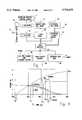
- FIG. 1is a block diagram of a two bits-per-cell semiconductor integrated circuit memory device having improved reading scheme, constructed in accordance with the principles of the present invention
- FIG. 2is a graph of four memory states for a cell storing two bits-per-cell and the corresponding threshold voltage distributions for the three reference cells disposed therebetween;
- FIG. 3is a simplified block diagram of the read circuitry 110 of FIG. 1;
- FIG. 4shows the waveforms of various signals in FIG. 3, useful in understanding the read operation of the present invention.
- FIG. 1a block diagram of a two bits-per-cell semiconductor integrated circuit memory device 10 which includes an improved reading structure of the present invention for performing a read operation in an array of two bits-per-cell flash electrically erasable read-only memory (EEPROM) cells of the memory device so as to render enhanced efficiency.
- the improved reading structure and the remaining portions of the memory device 10are both wholly formed on a single semiconductor substrate by known CMOS integrated circuit technology.
- the two bits-per-cell semiconductor integrated circuit memory device 10includes a memory core cell array 12, a row address decoder 14, a column address decoder 16, a wordline risetime control circuit 17, an address input circuit 18, a Y-pass gate circuit 20, a reference cell array 22, and a reference Y-select circuit 24.
- the memory core cell array 12includes approximately 16 million core cells arranged in a regular matrix pattern of 2 12 rows and 2 12 columns. Preferably, groups of columns are formed such that each group defines a page. Each page represents a number of bytes of data. For instance, the 2 12 columns may be divided into four pages so that each page will contain 128 bytes (1024 bits) of data.
- a predetermined number of rowsmay be grouped together so as to form a sector defining a selectable block.
- the 2 12 rowsmay be divided into 64 sectors so that each sector will be composed of 64 rows.
- each sectorwill contain 32K bytes (256K bits) of data.
- the 16 Mb flash memory cellscan actually store 32 Mb of data since two bits of data per cell is being stored in order to provide a double density storing capacity.
- the effective sector sizeis 64K bytes.
- each of the memory core cellshas its threshold voltage set to one of three higher levels with respect to its control gate than a memory core cell which is not programmed but set in the erased state.
- FIG. 2there is shown a graph of four threshold voltage V t , distributions for the four possible states (three programmed states and an erased state) for the double density memory cells.
- the curve Ashows the threshold voltage distribution for the memory core cells in the erased state or corresponding to storing data or logic "11."
- the erase verify reference voltage of the erased stateis +1.2 V.
- the curve Bshows the voltage distribution for the memory core cells in the first programmed state (PGMVT1) or corresponds to storing data or logic "10.”
- the voltage PGMVT1 of the first programmed stateis in the range between +2.5 V to +2.7 V.
- the curve Cshows the threshold voltage distribution for the memory core cells in the second programmed state (PGMVT2) or corresponding to storing data or logic "01."
- the voltage PGMVT2 of the second programmed stateis in the range between +3.5 V to +3.7 V.
- the curve Dshows the threshold voltage distribution for memory core cells in the third programmed state (PGMVT3) or corresponding to storing data or logic "00.”
- the voltage PGMVT3 of the third programmed stateis in the range between +4.5 V to +4.7 V.
- the reference cell array 22includes a plurality of sets of reference columns. Each column in the sets of reference columns has 2 12 rows corresponding to the number of rows in the memory core cell array 12. Thus, there will be 2 12 rows in each of the sets of reference columns. Further, the number of the plurality of sets of reference columns corresponds to the number of possible programmed memory states of the memory core cell. For the two bits-per-cell memory device 10, there will be three sets of reference columns. In addition, the three sets of reference columns are embedded and are associated with every page in the memory core array 12 with dedicated bit lines so that the reference column cells can be programmed and erased along with the remainder of the selected page. In particular, when the page is being programmed, 128 bytes are usually programmed in parallel. Therefore, three reference columns of reference core cells are also concurrently programmed when the memory core cells are being programmed.
- the curve Eshows the threshold voltage distribution for the first reference level (REFVT1) in the first reference column.
- the voltage REFVT1 of the first reference levelis in the range between +2.0 V to +2.2 V.
- the curve Fshows the threshold voltage distribution for the second reference level (REFVT2) in the second reference column.
- the voltage REFVT2 of the second reference levelis in the range between +3.0 V to +3.2 V.
- the curve Gshows the threshold voltage distribution for the third reference level (REFVT3) in the third reference column.
- the voltage REFVT3 of the third reference levelis in the range between +4.0 V to +4.2 V.
- the memory cellhas the capability of storing two bits of data depending upon the value of the memory core threshold voltages.
- the reference core cellshas a reference level dependent upon the value of the reference threshold voltage.
- the threshold voltages for the respective curves A through D for each of the memory core cells of the two bits-per-cell flash memory deviceare not all identical to the threshold voltages on all other memory cells but varies in a typical Gausian or bell-shaped distribution.
- the respective curves E through Gare also in the form of a bell-shaped curve.
- Address signals A jare externally applied to the address input circuit 18.
- the row address signals from the address input circuit 18are fed to the row address decoder 14, and the column address signals thereof are fed to the column address decoder 16.
- the row address decoder 14selects certain ones of the plurality of word-lines in the memory core cell array 12 in response to the row address signals.
- the column address decoder 16selects one of the pages in the memory core array in response to the column address signals as well as the corresponding sets of reference columns associated with the selected page.
- the Y-pass gate circuit 20connects the corresponding array bit lines in the selected page with a read circuitry 110.
- the reference column select circuit 24sequentially selects and connects each of the corresponding reference bit lines of the reference cell array associated with the selected pages to the read circuitry 110.
- FIG. 3there is illustrated a simplified block diagram of a portion of the read circuitry 100a in FIG. 1 for use with one page (i.e., WL 1 of array 112) of the memory core array 12 with associated reference columns 122a, 122b and 122c of the reference cell array 22.
- the memory core cells MC11 through MCnm of the array 112are arranged in the form of a matrix.
- the core cells MC11, MC12, . . . MC1mare arranged in the same row and have their selection terminals connected to the same common wordline WL 1 .
- MC2mare arranged in the same row and have their selection terminals connected to the common wordline WL 2 . This is likewise done for each of the remaining rows in the block 112.
- the memory core cells MCn1, MCn2, . . . MCnmare arranged in the same row and have their selection terminals connected to the common wordline WLn.
- MCnmare arranged in the same respective columns and have their corresponding data terminals connected to associated common bit lines BL 1 , BL 2 , . . . BL n , respectively.
- the number nis equal to 64 for a sector
- the number mis equal to 1024 for a page containing 256 bytes of two bits-per-cell data.
- Each of the memory core cells MC11 through MCnmis comprised of one of the corresponding array floating gate transistors Q p11 -Q pnm .
- the array transistors Q p11 -Q pnmfunction as a memory transistor for storing data or logic levels "11,” “10,” “01,” or "00" therein.
- Each of the array transistorshas its gate connected to one of the rows of wordlines, its source connected to one of the columns of bit lines, and its drain connected to a page common array ground line VSS.
- the reference column 122ais comprised of a plurality of reference cells RC 11 , RC 21 , . . . RC n1 .
- Each of the reference cells RC 11 -RC n1is comprised of one of the corresponding reference cell transistors Q R11 -Q Rn1 .
- the reference column 122bis comprised of a plurality of reference cells RC 12 , RC 22 , . . . RC n2 .
- Each of the reference cells RC 12 -RC n2is comprised of one of the corresponding reference cell transistors Q R12 -Q Rn1 .
- the reference column 122cis comprised of a plurality of reference cells RC 13 , RC 23 , . .
- Each of the reference cells RC 13 -RC n3is comprised of one of the corresponding reference cell transistors Q R13 -Q Rn3 .
- the gates of the array transistors and the reference cell transistors located in the same row in the pageare connected to the same wordline.
- the gates of the array transistors Q P11 , Q P12 , . . . Q P1m and the gates of the reference cell transistors Q R11 , Q R12 , and Q R13are connected to the wordline WL 1 .
- each of the three reference cell transistorsis programmed to a different reference threshold level, each being programmed to have a reference level between two of the adjacent actual program states of the array core cell.
- a first reference core cellis set to a first reference level REFVT1 (curve E) located between the program logic level “10" and the erased logic level “11.”
- a second reference core cellis set to a reference voltage level REFVT2 (curve F) located between the program logic levels "01” and “10.”
- a third reference core cellis set to a reference voltage level REFVT3 located between the program levels "00" and "01.”
- the improved read circuitry 110ais essentially comprised of a differential pair amplifier 26, a latch 27, a reference bit line level detector 28, a reference selection circuit 30, a unity gain reference driver 32, and a bandgap reference generator 34.
- the unity gain reference driver 32has its input connected to a common reference bit line REFBL and has its output on line 124 for providing a reference bit line voltage REFBLX. Since the resistance and capacitance of the array bit lines and the reference bit lines are closely matched, the unity gain reference driver 32 serves to buffer the reference bit line and supplies a 1-to-1 voltage translation with minimal phase lag to the differential pair amplifier 26.
- the bandgap generator 34is used to produce a very stable bandgap reference derived voltage BGR on line 125 corresponding to a midpoint of the reference bit line voltage REFBLX while the reference bit line is being discharged.
- the reference bit line voltage level detector 28has a first input on line 126 for receiving the reference bit line voltage REFBLX and has a second input on line 128 for receiving the bandgap reference derived voltage BGR.
- the level detector 28generates a one-shot pulse signal STROBE on its output on line 130 when the reference bit line voltage REFBLX has discharged down to the bandgap reference derived voltage BGR during the read operation in order to turn on the latch 27.
- the reference selection circuit 30has a first input on line 132 for also receiving the reference bit line voltage REFBLX and has a second input on line 134 for also receiving the bandgap reference derived voltage BGR.
- the reference selection circuit 30also has a third input on line 136 for receiving a read enable signal READ and a fourth input on line 138 for receiving a program enable signal PGM. Dependent upon whether the read enable signal or program enable signal is active, the output of the reference selection circuit 30 on line 140 will selectively produce either the bandgap reference derived voltage BGR or the reference bit line voltage REFBLX.
- the differential pair amplifier 26functioning as a comparator has its non-inverting input connected to receive either the bandgap reference derived voltage BGR or the bit line reference voltage REFBLX and its inverting input connected to receive the array bit line voltage BL.
- the differential amplifier 26consists of a sense amplifier and has its output driving the latch 27.
- the output of the latch 27stores a logic "1” or "0" dependent upon whether the bit line signal BL is lower or higher than the reference bit line signal REFBLX during the read operation.
- bit line pre-charge circuit 36is used to precharge the selected array bit line via the Y-pass gate circuit 20 and the associated reference bit line via the reference Y-select circuit 24 to the same potential (i.e., +1.8 V) prior to the start of the read operation. This is illustrated by the waveforms A (array bit line BL) and B (reference bit line REFBLX) in FIG. 4 at time t0. These bit lines are then left floating by turning off the precharge devices.
- the wordline voltage on the wordline WL 1is allowed to ramp up at a speed which is at least ten times slower than the RC time constant of the array bit line. This function is accomplished by the wordline risetime control circuit 17 in FIG. 1. This is done so that all of the cells on the wordline will see the same potential at a given time, notwithstanding its location within the memory core array 112.
- the wordline voltage on the gates of the array core transistor Q P11 and the selected one of the reference core transistors Q R11 through Q R13exceeds its threshold voltage, the respective array bit line and reference bit line will begin to discharge, as shown at times t2 and t3, respectively.
- the rate of discharge of the array and reference bit lineswill be dependent strictly upon the threshold voltages of the array core cell and reference core cell, respectively.
- the differential amplifier 26will compare the threshold voltage of the core cell being read with respect to the threshold voltage of the selected reference cell and latches a logic "1" or "0,” dependent upon which is higher.
- an external signal RELwill be discharged to zero.
- the reference bit line voltage REFBLXdischarges halfway down at time t4a
- the reference bit line level detector 28will generate the signal STROBE on line 130 so as to turn on the latch 127.
- a window of approximately 50 ns(between times t4a and t6) is generated during which time the latching of the output of the differential amplifier 26 into the latch 27 must occur (e.g., time t5).
- the page buffer 38is also used during the page programming operation.
- a program verify operationis performed simultaneously while the page programming is in progress.
- An extended NOR gate circuit 40is used for generating a signal VERIFY on line 41 which goes to a high logic level when the whole page has been verified.
- the details of the circuits and operations thereof for the page buffer 38 and NOR gate circuit 40are described and illustrated in co-pending application Ser. No. 08/669,116 filed Jun. 24, 1996 and entitled "A Multiple Bits-Per-Cell Flash Shift Register Page Buffer," (attorney Docket No. 95A-1788) which is assigned to the same assignee as the present invention.
- the above-described read operationis performed three times in order to determine if a logic state "00,” “01,” “10,” or “11" is being stored.
- the latch 27will store a logic "1" since the programmed voltage PGMVT3 is higher than the second reference voltage REFVT2.
- the reference voltage REFVT1 programmed into the reference cell RC 11is selected to be used as the reference voltage REFBLX by the reference Y-select circuit 24.
- the latchwill again store a logic "1” since the programmed voltage PGMVT3 is higher than the reference voltage REFVT1.
- the reference voltage REFVT3is selected by the reference Y-select circuit 24 to be used as the reference voltage REFBLX.
- the latch 27will store a logic "1" during this third read operation since the programmed voltage PGMVT3 is greater than the reference voltage REFVT3.
- the improved read circuitry 110 of the present inventionwhile described with respect to a two bits-per-cell memory core array, is also applicable to multiple bits-per-cell memory core arrays storing more than two bits of data per cell.
- each of the memory core cellswould then be programmed to any multiple number of threshold levels so that each cell can store any number of bits of information.
- the present inventionprovides an improved read circuitry for performing a read operation in an array of two bits-per-cell flash EEPROM memory cells so as to render enhanced efficiency.
- the read circuitryincludes reference cell transistors which are programmed at the same time as the memory core transistors are being programmed.
- a differential pair amplifier and latch combinationis responsive to a strobe signal for comparing the threshold voltage of the selected memory core cells with each of the reference cell threshold voltages so as to determine which one of the plurality of memory states the selected memory core cell is storing.
Landscapes
- Engineering & Computer Science (AREA)
- Computer Hardware Design (AREA)
- Read Only Memory (AREA)
Abstract
Description
Claims (9)
Priority Applications (1)
| Application Number | Priority Date | Filing Date | Title |
|---|---|---|---|
| US08/884,547US5754475A (en) | 1996-06-24 | 1997-06-27 | Bit line discharge method for reading a multiple bits-per-cell flash EEPROM |
Applications Claiming Priority (2)
| Application Number | Priority Date | Filing Date | Title |
|---|---|---|---|
| US66879596A | 1996-06-24 | 1996-06-24 | |
| US08/884,547US5754475A (en) | 1996-06-24 | 1997-06-27 | Bit line discharge method for reading a multiple bits-per-cell flash EEPROM |
Related Parent Applications (1)
| Application Number | Title | Priority Date | Filing Date |
|---|---|---|---|
| US66879596AContinuation | 1996-06-24 | 1996-06-24 |
Publications (1)
| Publication Number | Publication Date |
|---|---|
| US5754475Atrue US5754475A (en) | 1998-05-19 |
Family
ID=24683776
Family Applications (1)
| Application Number | Title | Priority Date | Filing Date |
|---|---|---|---|
| US08/884,547Expired - LifetimeUS5754475A (en) | 1996-06-24 | 1997-06-27 | Bit line discharge method for reading a multiple bits-per-cell flash EEPROM |
Country Status (5)
| Country | Link |
|---|---|
| US (1) | US5754475A (en) |
| EP (1) | EP0907954B1 (en) |
| DE (1) | DE69702256T2 (en) |
| TW (1) | TW316311B (en) |
| WO (1) | WO1997050089A1 (en) |
Cited By (108)
| Publication number | Priority date | Publication date | Assignee | Title |
|---|---|---|---|---|
| US5889698A (en)* | 1995-01-31 | 1999-03-30 | Hitachi, Ltd. | Nonvolatile memory device and refreshing method |
| US5943286A (en)* | 1996-08-09 | 1999-08-24 | Nec Corporation | Memory device having a plurality of cell array blocks including reference cells are connected in series |
| US5959882A (en)* | 1996-07-10 | 1999-09-28 | Hitachi, Ltd. | Nonvolatile semiconductor memory device and data writing method therefor |
| US6011725A (en)* | 1997-08-01 | 2000-01-04 | Saifun Semiconductors, Ltd. | Two bit non-volatile electrically erasable and programmable semiconductor memory cell utilizing asymmetrical charge trapping |
| US6038169A (en)* | 1999-03-18 | 2000-03-14 | Halo Lsi Design & Device Technology, Inc. | Read reference scheme for flash memory |
| US6108259A (en)* | 1998-06-12 | 2000-08-22 | Samsung Electronics, Co., Ltd. | Nonvolatile semiconductor memory device |
| US6160440A (en)* | 1998-09-25 | 2000-12-12 | Intel Corporation | Scaleable charge pump for use with a low voltage power supply |
| US6163484A (en)* | 1998-04-27 | 2000-12-19 | Nec Corporation | Non-volatile semiconductor storage device having improved program/erase/over erase verify |
| US6172912B1 (en)* | 1998-06-30 | 2001-01-09 | Sharp Kabushiki Kaisha | Programming method for a nonvolatile semiconductor memory |
| US6226213B1 (en)* | 2000-01-31 | 2001-05-01 | Taiwan Semiconductor Manufacturing Co., Ltd. | Reference cell array to generate the reference current for sense amplifier |
| US6304486B1 (en)* | 1999-12-20 | 2001-10-16 | Fujitsu Limited | Sensing time control device and method |
| US6320785B1 (en) | 1996-07-10 | 2001-11-20 | Hitachi, Ltd. | Nonvolatile semiconductor memory device and data writing method therefor |
| US6324112B1 (en)* | 1999-11-18 | 2001-11-27 | Stmicroelectronics S.A. | Reading device and method for integrated circuit memory |
| US6430077B1 (en) | 1997-12-12 | 2002-08-06 | Saifun Semiconductors Ltd. | Method for regulating read voltage level at the drain of a cell in a symmetric array |
| US20030043621A1 (en)* | 2001-06-14 | 2003-03-06 | Wong Sau Ching | Bit line reference circuits for binary and multiple-bit-per-cell memories |
| US6538922B1 (en) | 2000-09-27 | 2003-03-25 | Sandisk Corporation | Writable tracking cells |
| US6549473B2 (en)* | 2000-05-31 | 2003-04-15 | Stmicroelectronics S.R.L. | Circuital structure for reading data in a non-volatile memory device |
| US20030072192A1 (en)* | 2000-05-04 | 2003-04-17 | Ilan Bloom | Programming of nonvolatile memory cells |
| US6552387B1 (en) | 1997-07-30 | 2003-04-22 | Saifun Semiconductors Ltd. | Non-volatile electrically erasable and programmable semiconductor memory cell utilizing asymmetrical charge trapping |
| US6574158B1 (en) | 2001-09-27 | 2003-06-03 | Cypress Semiconductor Corp. | Method and system for measuring threshold of EPROM cells |
| US6584017B2 (en) | 2001-04-05 | 2003-06-24 | Saifun Semiconductors Ltd. | Method for programming a reference cell |
| US6583007B1 (en) | 2001-12-20 | 2003-06-24 | Saifun Semiconductors Ltd. | Reducing secondary injection effects |
| US20030117861A1 (en)* | 2001-12-20 | 2003-06-26 | Eduardo Maayan | NROM NOR array |
| US20030142544A1 (en)* | 2002-01-31 | 2003-07-31 | Eduardo Maayan | Mass storage array and methods for operation thereof |
| US6614692B2 (en) | 2001-01-18 | 2003-09-02 | Saifun Semiconductors Ltd. | EEPROM array and method for operation thereof |
| US6633499B1 (en) | 1997-12-12 | 2003-10-14 | Saifun Semiconductors Ltd. | Method for reducing voltage drops in symmetric array architectures |
| US6633496B2 (en) | 1997-12-12 | 2003-10-14 | Saifun Semiconductors Ltd. | Symmetric architecture for memory cells having widely spread metal bit lines |
| US6636440B2 (en) | 2001-04-25 | 2003-10-21 | Saifun Semiconductors Ltd. | Method for operation of an EEPROM array, including refresh thereof |
| WO2003088259A1 (en)* | 2002-04-08 | 2003-10-23 | Advanced Micro Devices, Inc. | Refresh scheme for dynamic page programming |
| WO2003088260A1 (en)* | 2002-04-08 | 2003-10-23 | Advanced Micro Devices, Inc. | Algorithm dynamic reference programming |
| US6643181B2 (en) | 2001-10-24 | 2003-11-04 | Saifun Semiconductors Ltd. | Method for erasing a memory cell |
| US20030208663A1 (en)* | 2002-04-12 | 2003-11-06 | Van Buskirk Michael A. | System and method for multi-bit flash reads using dual dynamic references |
| US6677805B2 (en) | 2001-04-05 | 2004-01-13 | Saifun Semiconductors Ltd. | Charge pump stage with body effect minimization |
| US20040008541A1 (en)* | 2002-07-10 | 2004-01-15 | Eduardo Maayan | Multiple use memory chip |
| US20040022113A1 (en)* | 2002-08-01 | 2004-02-05 | Ran Dvir | High voltage insertion in flash memory cards |
| US6735120B2 (en)* | 2000-06-02 | 2004-05-11 | Fujitsu Limited | Semiconductor device having a high-speed data read operation |
| EP1271550A3 (en)* | 2001-06-20 | 2004-06-23 | Fujitsu Limited | Method and device for reading dual bit memory cells using multiple reference cells with two side read |
| US20040136220A1 (en)* | 2002-10-29 | 2004-07-15 | Guy Cohen | Method circuit and system for determining a reference voltage |
| US20040136236A1 (en)* | 2002-10-29 | 2004-07-15 | Guy Cohen | Method circuit and system for read error detection in a non-volatile memory array |
| US20040153620A1 (en)* | 2003-01-30 | 2004-08-05 | Shai Eisen | Address scramble |
| US6791396B2 (en) | 2001-10-24 | 2004-09-14 | Saifun Semiconductors Ltd. | Stack element circuit |
| US20040190340A1 (en)* | 2003-03-26 | 2004-09-30 | Yue-Der Chih | Word-line voltage generator |
| US20040218426A1 (en)* | 2003-04-29 | 2004-11-04 | Oleg Dadashev | Apparatus and methods for multi-level sensing in a memory array |
| US20040222437A1 (en)* | 2000-12-07 | 2004-11-11 | Dror Avni | Programming and erasing methods for an NROM array |
| US20040255090A1 (en)* | 2003-06-13 | 2004-12-16 | Guterman Daniel C. | Tracking cells for a memory system |
| US20040257873A1 (en)* | 2003-06-20 | 2004-12-23 | Ming-Huei Shieh | Memory with a core-based virtual ground and dynamic reference sensing scheme |
| US20050013164A1 (en)* | 2001-05-31 | 2005-01-20 | Semiconductor Energy Laboratory Co., Ltd. | Nonvolatile memory and method of driving the same |
| US20050057953A1 (en)* | 2003-09-16 | 2005-03-17 | Eli Lusky | Reading array cell with matched reference cell |
| US20050068807A1 (en)* | 2003-09-30 | 2005-03-31 | Takashi Ohsawa | Semiconductor integrated circuit device |
| US20050174853A1 (en)* | 2004-02-10 | 2005-08-11 | M-Systems Flash Disk Pioneers Ltd. | Two-phase programming of a flash memory |
| US20050232024A1 (en)* | 2004-04-19 | 2005-10-20 | Shahar Atir | Method for reading a memory array with neighbor effect cancellation |
| US20050275366A1 (en)* | 2004-06-10 | 2005-12-15 | Moteurs Leroy-Somer | Devices and methods for updating the programming of a system for controlling an electric rotary machine |
| US20060034122A1 (en)* | 2004-08-12 | 2006-02-16 | Yoram Betser | Dynamic matching of signal path and reference path for sensing |
| US20060036803A1 (en)* | 2004-08-16 | 2006-02-16 | Mori Edan | Non-volatile memory device controlled by a micro-controller |
| US20060056240A1 (en)* | 2004-04-01 | 2006-03-16 | Saifun Semiconductors, Ltd. | Method, circuit and system for erasing one or more non-volatile memory cells |
| US20060077736A1 (en)* | 2004-08-30 | 2006-04-13 | Harunobu Nakagawa | Semiconductor device, semiconductor device testing method, and programming method |
| US20060126382A1 (en)* | 2004-12-09 | 2006-06-15 | Eduardo Maayan | Method for reading non-volatile memory cells |
| US7113427B1 (en)* | 2005-03-09 | 2006-09-26 | National Semiconductor Corporation | NVM PMOS-cell with one erased and two programmed states |
| US20060227619A1 (en)* | 2005-04-12 | 2006-10-12 | Yasuhiko Honda | Nonvolatile semiconductor memory device which stores multivalue data |
| US20060279986A1 (en)* | 2005-05-30 | 2006-12-14 | Seiichi Suzuki | Semiconductor device and programming method therefor |
| US20060285408A1 (en)* | 2005-06-17 | 2006-12-21 | Saifun Semiconductors, Ltd. | Method circuit and system for compensating for temperature induced margin loss in non-volatile memory cells |
| US20060285386A1 (en)* | 2005-06-15 | 2006-12-21 | Saifun Semiconductors, Ltd. | Accessing an NROM array |
| US20070002632A1 (en)* | 2005-06-30 | 2007-01-04 | Renesas Technology Corp. | Semiconductor storage device having memory cell for storing data by using difference in threshold voltage |
| US20070030745A1 (en)* | 2005-08-05 | 2007-02-08 | Halo Lsi Inc. | Referencing scheme for trap memory |
| US20070036007A1 (en)* | 2005-08-09 | 2007-02-15 | Saifun Semiconductors, Ltd. | Sticky bit buffer |
| EP1763039A1 (en)* | 2005-09-09 | 2007-03-14 | Macronix International Co., Ltd. | Method and apparatus for protection from over-erasing nonvolatile memory cells |
| US7221138B2 (en) | 2005-09-27 | 2007-05-22 | Saifun Semiconductors Ltd | Method and apparatus for measuring charge pump output current |
| US20070121379A1 (en)* | 2005-11-30 | 2007-05-31 | Oki Electric Industry Co., Ltd. | Electrically writable nonvolatile memory |
| US20070133304A1 (en)* | 2005-12-08 | 2007-06-14 | Elite Semiconductor Memory Technology Inc. | Method and apparatus for determining sensing timing of flash memory |
| US20070255889A1 (en)* | 2006-03-22 | 2007-11-01 | Yoav Yogev | Non-volatile memory device and method of operating the device |
| US20070263438A1 (en)* | 2006-05-12 | 2007-11-15 | Elite Semiconductor Memory Technology Inc. | Method for reading NAND memory device and memory cell array thereof |
| US7301807B2 (en) | 2003-10-23 | 2007-11-27 | Sandisk Corporation | Writable tracking cells |
| US20070272090A1 (en)* | 2006-02-01 | 2007-11-29 | Bommaraju Tilak V | Hydrogen mitigation and energy generation with water-activated chemical heaters |
| US7317633B2 (en) | 2004-07-06 | 2008-01-08 | Saifun Semiconductors Ltd | Protection of NROM devices from charge damage |
| US7352627B2 (en) | 2006-01-03 | 2008-04-01 | Saifon Semiconductors Ltd. | Method, system, and circuit for operating a non-volatile memory array |
| US20080091878A1 (en)* | 2006-10-13 | 2008-04-17 | Spansion, Llc | Virtual memory card controller |
| US7369440B2 (en) | 2005-01-19 | 2008-05-06 | Saifun Semiconductors Ltd. | Method, circuit and systems for erasing one or more non-volatile memory cells |
| US20080192550A1 (en)* | 2007-02-13 | 2008-08-14 | Micron Technology, Inc. | Circuits, systems and methods for driving high and low voltages on bit lines in non-volatile memory |
| US7420848B2 (en) | 2002-01-31 | 2008-09-02 | Saifun Semiconductors Ltd. | Method, system, and circuit for operating a non-volatile memory array |
| US20080225600A1 (en)* | 2007-03-14 | 2008-09-18 | Hynix Semiconductor Inc. | Method of reading data in a non-volatile memory device |
| US20080239825A1 (en)* | 2007-03-30 | 2008-10-02 | Nec Electronics Corporation | Floating gate memory device with improved reference current generation |
| US7457183B2 (en) | 2003-09-16 | 2008-11-25 | Saifun Semiconductors Ltd. | Operating array cells with matched reference cells |
| US20090046521A1 (en)* | 2006-11-21 | 2009-02-19 | Macronix International Co., Ltd. | Memory structure, programming method and reading method therefor, and memory control circuit thereof |
| US20090052256A1 (en)* | 2007-08-20 | 2009-02-26 | Pantas Sutardja | Threshold voltage digitizer for array of programmable threshold transistors |
| US7535765B2 (en) | 2004-12-09 | 2009-05-19 | Saifun Semiconductors Ltd. | Non-volatile memory device and method for reading cells |
| US20090168578A1 (en)* | 2007-12-31 | 2009-07-02 | Simtek | Dummy cell for memory circuits |
| CN100524527C (en)* | 2005-09-09 | 2009-08-05 | 旺宏电子股份有限公司 | System and method for reference circuit in dual bit flash memory device |
| US7605579B2 (en) | 2006-09-18 | 2009-10-20 | Saifun Semiconductors Ltd. | Measuring and controlling current consumption and output current of charge pumps |
| US7638835B2 (en) | 2006-02-28 | 2009-12-29 | Saifun Semiconductors Ltd. | Double density NROM with nitride strips (DDNS) |
| US7638850B2 (en) | 2004-10-14 | 2009-12-29 | Saifun Semiconductors Ltd. | Non-volatile memory structure and method of fabrication |
| US7668017B2 (en) | 2005-08-17 | 2010-02-23 | Saifun Semiconductors Ltd. | Method of erasing non-volatile memory cells |
| US7675782B2 (en) | 2002-10-29 | 2010-03-09 | Saifun Semiconductors Ltd. | Method, system and circuit for programming a non-volatile memory array |
| US7692961B2 (en) | 2006-02-21 | 2010-04-06 | Saifun Semiconductors Ltd. | Method, circuit and device for disturb-control of programming nonvolatile memory cells by hot-hole injection (HHI) and by channel hot-electron (CHE) injection |
| US7701779B2 (en)* | 2006-04-27 | 2010-04-20 | Sajfun Semiconductors Ltd. | Method for programming a reference cell |
| US7743230B2 (en) | 2003-01-31 | 2010-06-22 | Saifun Semiconductors Ltd. | Memory array programming circuit and a method for using the circuit |
| US7760554B2 (en) | 2006-02-21 | 2010-07-20 | Saifun Semiconductors Ltd. | NROM non-volatile memory and mode of operation |
| US7786512B2 (en) | 2005-07-18 | 2010-08-31 | Saifun Semiconductors Ltd. | Dense non-volatile memory array and method of fabrication |
| US7808818B2 (en) | 2006-01-12 | 2010-10-05 | Saifun Semiconductors Ltd. | Secondary injection for NROM |
| US20110007565A1 (en)* | 1996-09-18 | 2011-01-13 | Katsuki Hazama | Multilevel semiconductor memory, write/read method thereto/therefrom and storage medium storing write/read program |
| US20110176378A1 (en)* | 2010-01-20 | 2011-07-21 | Macronix International Co., Ltd. | Memory Program Discharge Circuit |
| US8053812B2 (en) | 2005-03-17 | 2011-11-08 | Spansion Israel Ltd | Contact in planar NROM technology |
| US8253452B2 (en) | 2006-02-21 | 2012-08-28 | Spansion Israel Ltd | Circuit and method for powering up an integrated circuit and an integrated circuit utilizing same |
| US9659624B1 (en)* | 2016-03-15 | 2017-05-23 | Avago Technologies General Ip (Singapore) Pte. Ltd. | Method for sense reference generation for MTJ based memories |
| US20180047454A1 (en)* | 2013-03-15 | 2018-02-15 | Silicon Storage Technology, Inc. | High Speed Sensing For Advanced Nanometer Flash Memory Device |
| US20180130514A1 (en)* | 2015-02-17 | 2018-05-10 | Kilopass Technology, Inc. | MTP-Thyristor Memory Cell Circuits and Methods of Operation |
| US20200090764A1 (en)* | 2018-09-18 | 2020-03-19 | Toshiba Memory Corporation | Semiconductor memory device, memory system, and method |
| US11049564B2 (en) | 2019-03-13 | 2021-06-29 | Ememory Technology Inc. | Erasable programmable non-volatile memory |
| US11961570B2 (en)* | 2018-06-26 | 2024-04-16 | Vishal Sarin | Methods and systems of cell-array programming for neural compute using flash arrays |
Families Citing this family (1)
| Publication number | Priority date | Publication date | Assignee | Title |
|---|---|---|---|---|
| CN114664355B (en)* | 2022-03-16 | 2022-11-25 | 珠海博雅科技股份有限公司 | Reference current generating module and reference current setting method of nonvolatile memory |
Citations (7)
| Publication number | Priority date | Publication date | Assignee | Title |
|---|---|---|---|---|
| EP0358310A1 (en)* | 1988-08-12 | 1990-03-14 | Black & Decker Inc. | Soleplate for steam iron |
| US5029135A (en)* | 1989-02-15 | 1991-07-02 | Ricoh Company, Ltd. | Semiconductor memory apparatus with internal synchronization |
| US5157626A (en)* | 1989-11-21 | 1992-10-20 | Nec Corporation | Semiconductor memory |
| US5258958A (en)* | 1989-06-12 | 1993-11-02 | Kabushiki Kaisha Toshiba | Semiconductor memory device |
| US5386132A (en)* | 1992-11-02 | 1995-01-31 | Wong; Chun C. D. | Multimedia storage system with highly compact memory device |
| US5532962A (en)* | 1992-05-20 | 1996-07-02 | Sandisk Corporation | Soft errors handling in EEPROM devices |
| EP0756287A2 (en)* | 1989-04-13 | 1997-01-29 | SanDisk Corporation | A memory sensing circuit employing multi-current mirrors |
Family Cites Families (1)
| Publication number | Priority date | Publication date | Assignee | Title |
|---|---|---|---|---|
| JP2573335B2 (en)* | 1988-11-09 | 1997-01-22 | 株式会社東芝 | Non-volatile memory |
- 1997
- 1997-01-31DEDE69702256Tpatent/DE69702256T2/ennot_activeExpired - Lifetime
- 1997-01-31EPEP97904230Apatent/EP0907954B1/ennot_activeExpired - Lifetime
- 1997-01-31WOPCT/US1997/001822patent/WO1997050089A1/enactiveIP Right Grant
- 1997-02-05TWTW086101407Apatent/TW316311B/ennot_activeIP Right Cessation
- 1997-06-27USUS08/884,547patent/US5754475A/ennot_activeExpired - Lifetime
Patent Citations (7)
| Publication number | Priority date | Publication date | Assignee | Title |
|---|---|---|---|---|
| EP0358310A1 (en)* | 1988-08-12 | 1990-03-14 | Black & Decker Inc. | Soleplate for steam iron |
| US5029135A (en)* | 1989-02-15 | 1991-07-02 | Ricoh Company, Ltd. | Semiconductor memory apparatus with internal synchronization |
| EP0756287A2 (en)* | 1989-04-13 | 1997-01-29 | SanDisk Corporation | A memory sensing circuit employing multi-current mirrors |
| US5258958A (en)* | 1989-06-12 | 1993-11-02 | Kabushiki Kaisha Toshiba | Semiconductor memory device |
| US5157626A (en)* | 1989-11-21 | 1992-10-20 | Nec Corporation | Semiconductor memory |
| US5532962A (en)* | 1992-05-20 | 1996-07-02 | Sandisk Corporation | Soft errors handling in EEPROM devices |
| US5386132A (en)* | 1992-11-02 | 1995-01-31 | Wong; Chun C. D. | Multimedia storage system with highly compact memory device |
Cited By (252)
| Publication number | Priority date | Publication date | Assignee | Title |
|---|---|---|---|---|
| US20040179399A1 (en)* | 1995-01-31 | 2004-09-16 | Hitoshi Miwa | Clock synchronized nonvolatile memory device |
| US7542339B2 (en) | 1995-01-31 | 2009-06-02 | Solid State Storage Solutions, Llc | Clock synchronized non-volatile memory device |
| US6912156B2 (en) | 1995-01-31 | 2005-06-28 | Renesas Technology Corp. | Clock synchronized nonvolatile memory device |
| US6868006B2 (en) | 1995-01-31 | 2005-03-15 | Renesas Technology Corp. | Clock synchronized non-volatile memory device |
| US6038167A (en)* | 1995-01-31 | 2000-03-14 | Hitachi, Ltd. | Nonvolatile memory device and refreshing method |
| US6850434B2 (en) | 1995-01-31 | 2005-02-01 | Renesas Technology Corp. | Clock synchronized nonvolatile memory device |
| US6847549B2 (en) | 1995-01-31 | 2005-01-25 | Renesas Technology Corp. | Clock synchronized non-volatile memory device |
| US6111790A (en)* | 1995-01-31 | 2000-08-29 | Hitachi, Ltd. | Non-volatile memory device and refreshing method |
| US20050162940A1 (en)* | 1995-01-31 | 2005-07-28 | Hitoshi Miwa | Clock synchronized nonvolatile memory device |
| US6829163B2 (en) | 1995-01-31 | 2004-12-07 | Hitachi, Ltd. | Clock synchronized nonvolatile memory device |
| US6166949A (en)* | 1995-01-31 | 2000-12-26 | Hitachi, Ltd. | Nonvolatile memory device and refreshing method |
| US6965525B2 (en) | 1995-01-31 | 2005-11-15 | Renesas Technology Corp. | Clock synchronized nonvolatile memory device |
| US6804147B2 (en) | 1995-01-31 | 2004-10-12 | Renesas Technology Corp. | Clock synchronized non-volatile memory device |
| US6226198B1 (en) | 1995-01-31 | 2001-05-01 | Hitachi, Ltd. | Nonvolatile memory device and refreshing method |
| US6256230B1 (en) | 1995-01-31 | 2001-07-03 | Hitachi, Ltd. | Nonvolatile memory device and refreshing method |
| US6801452B2 (en) | 1995-01-31 | 2004-10-05 | Renesas Technology Corp. | Clock synchronized non-volatile memory device |
| US5889698A (en)* | 1995-01-31 | 1999-03-30 | Hitachi, Ltd. | Nonvolatile memory device and refreshing method |
| US20040184317A1 (en)* | 1995-01-31 | 2004-09-23 | Hitoshi Miwa | Clock synchronized nonvolatile memory device |
| US6366495B2 (en) | 1995-01-31 | 2002-04-02 | Hitachi, Ltd. | Nonvolatile memory device and refreshing method |
| US20040179384A1 (en)* | 1995-01-31 | 2004-09-16 | Hitoshi Miwa | Clock synchronized nonvolatile memory device |
| US6898118B2 (en) | 1995-01-31 | 2005-05-24 | Renesas Technology Corp. | Clock synchronized non-volatile memory device |
| US6459614B1 (en) | 1995-01-31 | 2002-10-01 | Hitachi, Ltd. | Non-volatile memory device and refreshing method |
| US20030035317A1 (en)* | 1995-01-31 | 2003-02-20 | Hitoshi Miwa | Nonvolatile memory device and refreshing method |
| US20040179400A1 (en)* | 1995-01-31 | 2004-09-16 | Hitoshi Miwa | Clock synchronized nonvolatile memory device |
| US8804431B2 (en) | 1995-01-31 | 2014-08-12 | S4, Inc. | Clock synchronized non-volatile memory device |
| US20060198201A1 (en)* | 1995-01-31 | 2006-09-07 | Hitoshi Miwa | Multi-bits storage memory |
| US20040174743A1 (en)* | 1995-01-31 | 2004-09-09 | Hitoshi Miwa | Clock synchronized nonvolatile memory device |
| US7161830B2 (en) | 1995-01-31 | 2007-01-09 | Renesas Technology Corp. | Clock synchronized nonvolatile memory device |
| US6768672B2 (en) | 1995-01-31 | 2004-07-27 | Renesas Technology Corp. | Clock Synchronized Non-Volatile Memory Device |
| US7193894B2 (en) | 1995-01-31 | 2007-03-20 | Renesas Technology Corp. | Clock synchronized nonvolatile memory device |
| US6757194B2 (en) | 1995-01-31 | 2004-06-29 | Renesas Technology Corp. | Clock synchronized non-volatile memory device |
| US20070064483A1 (en)* | 1995-01-31 | 2007-03-22 | Hitoshi Miwa | Clock synchronized non-volatile memory device |
| US6751119B2 (en) | 1995-01-31 | 2004-06-15 | Renesas Technology Corp. | Clock synchronized non-volatile memory device |
| US6751120B2 (en) | 1995-01-31 | 2004-06-15 | Renesas Technology Corp. | Clock synchronized non-volatile memory device |
| US20100020615A1 (en)* | 1995-01-31 | 2010-01-28 | Hitoshi Miwa | Clock synchronized non-volatile memory device |
| US20030147284A1 (en)* | 1995-01-31 | 2003-08-07 | Hitoshi Miwa | Nonvolatile memory device and refreshing method |
| US6747941B2 (en) | 1995-01-31 | 2004-06-08 | Renesas Technology Corp. | Clock synchronized non-volatile memory device |
| US7286397B2 (en) | 1995-01-31 | 2007-10-23 | Renesas Technology Corporation | Clock synchronized nonvolatile memory device |
| US7324375B2 (en) | 1995-01-31 | 2008-01-29 | Solid State Storage Solutions, Llc | Multi-bits storage memory |
| US7327604B2 (en) | 1995-01-31 | 2008-02-05 | Renesas Technology Corporation | Clock synchronized non-volatile memory device |
| US6525960B2 (en) | 1996-07-10 | 2003-02-25 | Hitachi, Ltd. | Nonvolatile semiconductor memory device including correction of erratic memory cell data |
| US20030185056A1 (en)* | 1996-07-10 | 2003-10-02 | Keiichi Yoshida | Nonvolatile semiconductor memory device and data writing method therefor |
| US6906952B2 (en) | 1996-07-10 | 2005-06-14 | Renesas Technology Corp. | Nonvolatile semiconductor memory device and data writing method therefor |
| US5959882A (en)* | 1996-07-10 | 1999-09-28 | Hitachi, Ltd. | Nonvolatile semiconductor memory device and data writing method therefor |
| USRE44350E1 (en) | 1996-07-10 | 2013-07-09 | Renesas Electronics Corporation | Nonvolatile semiconductor memory including multi-threshold voltage memory cells including voltage ranges indicating either an erase state or a two or more program state |
| US6320785B1 (en) | 1996-07-10 | 2001-11-20 | Hitachi, Ltd. | Nonvolatile semiconductor memory device and data writing method therefor |
| US5943286A (en)* | 1996-08-09 | 1999-08-24 | Nec Corporation | Memory device having a plurality of cell array blocks including reference cells are connected in series |
| US20110007565A1 (en)* | 1996-09-18 | 2011-01-13 | Katsuki Hazama | Multilevel semiconductor memory, write/read method thereto/therefrom and storage medium storing write/read program |
| US8707130B2 (en)* | 1996-09-18 | 2014-04-22 | Intellectual Ventures I Llc | Multilevel semiconductor memory, write/read method thereto/therefrom and storage medium storing write/read program |
| US6552387B1 (en) | 1997-07-30 | 2003-04-22 | Saifun Semiconductors Ltd. | Non-volatile electrically erasable and programmable semiconductor memory cell utilizing asymmetrical charge trapping |
| US6803299B2 (en) | 1997-07-30 | 2004-10-12 | Saifun Semiconductors Ltd. | Non-volatile electrically erasable and programmable semiconductor memory cell utilizing asymmetrical charge trapping |
| US6566699B2 (en) | 1997-07-30 | 2003-05-20 | Saifun Semiconductors Ltd. | Non-volatile electrically erasable and programmable semiconductor memory cell utilizing asymmetrical charge trapping |
| US20030201477A1 (en)* | 1997-07-30 | 2003-10-30 | Boaz Eitan | Non-volatile electrically erasable and programmable semiconductor memory cell utilizing asymmetrical charge trapping |
| US6011725A (en)* | 1997-08-01 | 2000-01-04 | Saifun Semiconductors, Ltd. | Two bit non-volatile electrically erasable and programmable semiconductor memory cell utilizing asymmetrical charge trapping |
| US6649972B2 (en) | 1997-08-01 | 2003-11-18 | Saifun Semiconductors Ltd. | Two bit non-volatile electrically erasable and programmable semiconductor memory cell utilizing asymmetrical charge trapping |
| US6768165B1 (en)* | 1997-08-01 | 2004-07-27 | Saifun Semiconductors Ltd. | Two bit non-volatile electrically erasable and programmable semiconductor memory cell utilizing asymmetrical charge trapping |
| US7405969B2 (en) | 1997-08-01 | 2008-07-29 | Saifun Semiconductors Ltd. | Non-volatile memory cell and non-volatile memory devices |
| US6633499B1 (en) | 1997-12-12 | 2003-10-14 | Saifun Semiconductors Ltd. | Method for reducing voltage drops in symmetric array architectures |
| US6633496B2 (en) | 1997-12-12 | 2003-10-14 | Saifun Semiconductors Ltd. | Symmetric architecture for memory cells having widely spread metal bit lines |
| US6430077B1 (en) | 1997-12-12 | 2002-08-06 | Saifun Semiconductors Ltd. | Method for regulating read voltage level at the drain of a cell in a symmetric array |
| US6163484A (en)* | 1998-04-27 | 2000-12-19 | Nec Corporation | Non-volatile semiconductor storage device having improved program/erase/over erase verify |
| US6108259A (en)* | 1998-06-12 | 2000-08-22 | Samsung Electronics, Co., Ltd. | Nonvolatile semiconductor memory device |
| US6172912B1 (en)* | 1998-06-30 | 2001-01-09 | Sharp Kabushiki Kaisha | Programming method for a nonvolatile semiconductor memory |
| US6160440A (en)* | 1998-09-25 | 2000-12-12 | Intel Corporation | Scaleable charge pump for use with a low voltage power supply |
| US6038169A (en)* | 1999-03-18 | 2000-03-14 | Halo Lsi Design & Device Technology, Inc. | Read reference scheme for flash memory |
| US6324112B1 (en)* | 1999-11-18 | 2001-11-27 | Stmicroelectronics S.A. | Reading device and method for integrated circuit memory |
| US6392943B2 (en) | 1999-11-18 | 2002-05-21 | Stmicroelectronics S.A. | Reading device and method for integrated circuit memory |
| US6304486B1 (en)* | 1999-12-20 | 2001-10-16 | Fujitsu Limited | Sensing time control device and method |
| US6226213B1 (en)* | 2000-01-31 | 2001-05-01 | Taiwan Semiconductor Manufacturing Co., Ltd. | Reference cell array to generate the reference current for sense amplifier |
| US6829172B2 (en) | 2000-05-04 | 2004-12-07 | Saifun Semiconductors Ltd. | Programming of nonvolatile memory cells |
| US6937521B2 (en) | 2000-05-04 | 2005-08-30 | Saifun Semiconductors Ltd. | Programming and erasing methods for a non-volatile memory cell |
| US20030072192A1 (en)* | 2000-05-04 | 2003-04-17 | Ilan Bloom | Programming of nonvolatile memory cells |
| US6549473B2 (en)* | 2000-05-31 | 2003-04-15 | Stmicroelectronics S.R.L. | Circuital structure for reading data in a non-volatile memory device |
| US6735120B2 (en)* | 2000-06-02 | 2004-05-11 | Fujitsu Limited | Semiconductor device having a high-speed data read operation |
| US6928000B2 (en) | 2000-06-02 | 2005-08-09 | Fujitsu Limited | Semiconductor memory device having a resistance adjustment unit |
| US20040196712A1 (en)* | 2000-06-02 | 2004-10-07 | Fujitsu Limited | Semiconductor memory device |
| US20040105307A1 (en)* | 2000-09-27 | 2004-06-03 | Khalid Shahzad B. | Writable tracking cells |
| US6714449B2 (en) | 2000-09-27 | 2004-03-30 | Sandisk Corporation | Sense amplifier suitable for analogue voltage levels |
| US6873549B2 (en) | 2000-09-27 | 2005-03-29 | Sandisk Corporation | Writable tracking cells |
| US6538922B1 (en) | 2000-09-27 | 2003-03-25 | Sandisk Corporation | Writable tracking cells |
| US20040222437A1 (en)* | 2000-12-07 | 2004-11-11 | Dror Avni | Programming and erasing methods for an NROM array |
| US6928001B2 (en) | 2000-12-07 | 2005-08-09 | Saifun Semiconductors Ltd. | Programming and erasing methods for a non-volatile memory cell |
| US6614692B2 (en) | 2001-01-18 | 2003-09-02 | Saifun Semiconductors Ltd. | EEPROM array and method for operation thereof |
| US7518908B2 (en) | 2001-01-18 | 2009-04-14 | Saifun Semiconductors Ltd. | EEPROM array and method for operation thereof |
| US7064983B2 (en) | 2001-04-05 | 2006-06-20 | Saifum Semiconductors Ltd. | Method for programming a reference cell |
| US6584017B2 (en) | 2001-04-05 | 2003-06-24 | Saifun Semiconductors Ltd. | Method for programming a reference cell |
| US20040130385A1 (en)* | 2001-04-05 | 2004-07-08 | Shor Joseph S. | Charge pump stage with body effect minimization |
| US6864739B2 (en) | 2001-04-05 | 2005-03-08 | Saifun Semiconductors Ltd. | Charge pump stage with body effect minimization |
| US6677805B2 (en) | 2001-04-05 | 2004-01-13 | Saifun Semiconductors Ltd. | Charge pump stage with body effect minimization |
| US6636440B2 (en) | 2001-04-25 | 2003-10-21 | Saifun Semiconductors Ltd. | Method for operation of an EEPROM array, including refresh thereof |
| US20050013164A1 (en)* | 2001-05-31 | 2005-01-20 | Semiconductor Energy Laboratory Co., Ltd. | Nonvolatile memory and method of driving the same |
| US6947327B2 (en)* | 2001-05-31 | 2005-09-20 | Semiconductor Energy Laboratory Co., Ltd. | Nonvolatile memory and method of driving the same |
| US20080019191A1 (en)* | 2001-05-31 | 2008-01-24 | Semiconductor Energy Laboratory Co., Ltd. | Nonvolatile memory and method of driving the same |
| US7372737B2 (en) | 2001-05-31 | 2008-05-13 | Semiconductor Energy Laboratory Co., Ltd. | Nonvolatile memory and method of driving the same |
| US7173858B2 (en) | 2001-05-31 | 2007-02-06 | Semiconductor Energy Laboratory Co., Ltd. | Nonvolatile memory and method of driving the same |
| US7099188B1 (en) | 2001-06-14 | 2006-08-29 | Samsung Electronics Co., Ltd. | Bit line reference circuits for binary and multiple-bit-per-cell memories |
| US20030043621A1 (en)* | 2001-06-14 | 2003-03-06 | Wong Sau Ching | Bit line reference circuits for binary and multiple-bit-per-cell memories |
| US6906951B2 (en)* | 2001-06-14 | 2005-06-14 | Multi Level Memory Technology | Bit line reference circuits for binary and multiple-bit-per-cell memories |
| EP1271550A3 (en)* | 2001-06-20 | 2004-06-23 | Fujitsu Limited | Method and device for reading dual bit memory cells using multiple reference cells with two side read |
| US6574158B1 (en) | 2001-09-27 | 2003-06-03 | Cypress Semiconductor Corp. | Method and system for measuring threshold of EPROM cells |
| US6888757B2 (en) | 2001-10-24 | 2005-05-03 | Saifun Semiconductors Ltd. | Method for erasing a memory cell |
| US6791396B2 (en) | 2001-10-24 | 2004-09-14 | Saifun Semiconductors Ltd. | Stack element circuit |
| US6643181B2 (en) | 2001-10-24 | 2003-11-04 | Saifun Semiconductors Ltd. | Method for erasing a memory cell |
| US20040233771A1 (en)* | 2001-10-24 | 2004-11-25 | Shor Joseph S. | Stack element circuit |
| US20030117861A1 (en)* | 2001-12-20 | 2003-06-26 | Eduardo Maayan | NROM NOR array |
| US6583007B1 (en) | 2001-12-20 | 2003-06-24 | Saifun Semiconductors Ltd. | Reducing secondary injection effects |
| US6885585B2 (en) | 2001-12-20 | 2005-04-26 | Saifun Semiconductors Ltd. | NROM NOR array |
| US6975536B2 (en) | 2002-01-31 | 2005-12-13 | Saifun Semiconductors Ltd. | Mass storage array and methods for operation thereof |
| US20030142544A1 (en)* | 2002-01-31 | 2003-07-31 | Eduardo Maayan | Mass storage array and methods for operation thereof |
| US7420848B2 (en) | 2002-01-31 | 2008-09-02 | Saifun Semiconductors Ltd. | Method, system, and circuit for operating a non-volatile memory array |
| WO2003088260A1 (en)* | 2002-04-08 | 2003-10-23 | Advanced Micro Devices, Inc. | Algorithm dynamic reference programming |
| US6690602B1 (en) | 2002-04-08 | 2004-02-10 | Advanced Micro Devices, Inc. | Algorithm dynamic reference programming |
| WO2003088259A1 (en)* | 2002-04-08 | 2003-10-23 | Advanced Micro Devices, Inc. | Refresh scheme for dynamic page programming |
| US6700815B2 (en) | 2002-04-08 | 2004-03-02 | Advanced Micro Devices, Inc. | Refresh scheme for dynamic page programming |
| GB2401971B (en)* | 2002-04-08 | 2005-06-22 | Advanced Micro Devices Inc | Algorithm dynamic reference programming |
| GB2401971A (en)* | 2002-04-08 | 2004-11-24 | Advanced Micro Devices Inc | Algorithm dynamic reference programming |
| CN1647214B (en)* | 2002-04-08 | 2010-04-28 | 斯班逊有限公司 | Refresh scheme for dynamic page programming |
| US6799256B2 (en)* | 2002-04-12 | 2004-09-28 | Advanced Micro Devices, Inc. | System and method for multi-bit flash reads using dual dynamic references |
| US20030208663A1 (en)* | 2002-04-12 | 2003-11-06 | Van Buskirk Michael A. | System and method for multi-bit flash reads using dual dynamic references |
| US7103706B1 (en)* | 2002-04-12 | 2006-09-05 | Spansion Llc | System and method for multi-bit flash reads using dual dynamic references |
| US7738304B2 (en) | 2002-07-10 | 2010-06-15 | Saifun Semiconductors Ltd. | Multiple use memory chip |
| US6917544B2 (en) | 2002-07-10 | 2005-07-12 | Saifun Semiconductors Ltd. | Multiple use memory chip |
| US20040008541A1 (en)* | 2002-07-10 | 2004-01-15 | Eduardo Maayan | Multiple use memory chip |
| US20040022113A1 (en)* | 2002-08-01 | 2004-02-05 | Ran Dvir | High voltage insertion in flash memory cards |
| US6826107B2 (en) | 2002-08-01 | 2004-11-30 | Saifun Semiconductors Ltd. | High voltage insertion in flash memory cards |
| US6992932B2 (en)* | 2002-10-29 | 2006-01-31 | Saifun Semiconductors Ltd | Method circuit and system for read error detection in a non-volatile memory array |
| US20040136220A1 (en)* | 2002-10-29 | 2004-07-15 | Guy Cohen | Method circuit and system for determining a reference voltage |
| US6963505B2 (en) | 2002-10-29 | 2005-11-08 | Aifun Semiconductors Ltd. | Method circuit and system for determining a reference voltage |
| US7675782B2 (en) | 2002-10-29 | 2010-03-09 | Saifun Semiconductors Ltd. | Method, system and circuit for programming a non-volatile memory array |
| US20040136236A1 (en)* | 2002-10-29 | 2004-07-15 | Guy Cohen | Method circuit and system for read error detection in a non-volatile memory array |
| US6967896B2 (en) | 2003-01-30 | 2005-11-22 | Saifun Semiconductors Ltd | Address scramble |
| US20040153620A1 (en)* | 2003-01-30 | 2004-08-05 | Shai Eisen | Address scramble |
| US7743230B2 (en) | 2003-01-31 | 2010-06-22 | Saifun Semiconductors Ltd. | Memory array programming circuit and a method for using the circuit |
| US6906958B2 (en)* | 2003-03-26 | 2005-06-14 | Taiwan Semiconductor Manufacturing Co., Ltd. | Word-line voltage generator |
| US20040190340A1 (en)* | 2003-03-26 | 2004-09-30 | Yue-Der Chih | Word-line voltage generator |
| US7142464B2 (en) | 2003-04-29 | 2006-11-28 | Saifun Semiconductors Ltd. | Apparatus and methods for multi-level sensing in a memory array |
| US20040218426A1 (en)* | 2003-04-29 | 2004-11-04 | Oleg Dadashev | Apparatus and methods for multi-level sensing in a memory array |
| US7916552B2 (en) | 2003-06-13 | 2011-03-29 | Sandisk Corporation | Tracking cells for a memory system |
| US20110141816A1 (en)* | 2003-06-13 | 2011-06-16 | Sandisk Corporation | Tracking Cells For A Memory System |
| US7237074B2 (en) | 2003-06-13 | 2007-06-26 | Sandisk Corporation | Tracking cells for a memory system |
| US20100202199A1 (en)* | 2003-06-13 | 2010-08-12 | Guterman Daniel C | Tracking cells for a memory system |
| US20040255090A1 (en)* | 2003-06-13 | 2004-12-16 | Guterman Daniel C. | Tracking cells for a memory system |
| US8072817B2 (en) | 2003-06-13 | 2011-12-06 | Sandisk Technologies Inc. | Tracking cells for a memory system |
| US7606068B2 (en) | 2003-06-20 | 2009-10-20 | Spansion Llc | Memory with a core-based virtual ground and dynamic reference sensing scheme |
| US20040257873A1 (en)* | 2003-06-20 | 2004-12-23 | Ming-Huei Shieh | Memory with a core-based virtual ground and dynamic reference sensing scheme |
| US7324374B2 (en)* | 2003-06-20 | 2008-01-29 | Spansion Llc | Memory with a core-based virtual ground and dynamic reference sensing scheme |
| US20080117678A1 (en)* | 2003-06-20 | 2008-05-22 | Spansion Llc | Memory with a core-based virtual ground and dynamic reference sensing scheme |
| US6954393B2 (en) | 2003-09-16 | 2005-10-11 | Saifun Semiconductors Ltd. | Reading array cell with matched reference cell |
| US20050057953A1 (en)* | 2003-09-16 | 2005-03-17 | Eli Lusky | Reading array cell with matched reference cell |
| US7864612B2 (en) | 2003-09-16 | 2011-01-04 | Spansion Israel Ltd | Reading array cell with matched reference cell |
| US7457183B2 (en) | 2003-09-16 | 2008-11-25 | Saifun Semiconductors Ltd. | Operating array cells with matched reference cells |
| US20050068807A1 (en)* | 2003-09-30 | 2005-03-31 | Takashi Ohsawa | Semiconductor integrated circuit device |
| US7123509B2 (en)* | 2003-09-30 | 2006-10-17 | Kabushiki Kaisha Toshiba | Floating body cell memory and reading and writing circuit thereof |
| US7301807B2 (en) | 2003-10-23 | 2007-11-27 | Sandisk Corporation | Writable tracking cells |
| US7177200B2 (en)* | 2004-02-10 | 2007-02-13 | Msystems Ltd. | Two-phase programming of a flash memory |
| US20050174853A1 (en)* | 2004-02-10 | 2005-08-11 | M-Systems Flash Disk Pioneers Ltd. | Two-phase programming of a flash memory |
| US7532529B2 (en) | 2004-03-29 | 2009-05-12 | Saifun Semiconductors Ltd. | Apparatus and methods for multi-level sensing in a memory array |
| US20060056240A1 (en)* | 2004-04-01 | 2006-03-16 | Saifun Semiconductors, Ltd. | Method, circuit and system for erasing one or more non-volatile memory cells |
| US7652930B2 (en) | 2004-04-01 | 2010-01-26 | Saifun Semiconductors Ltd. | Method, circuit and system for erasing one or more non-volatile memory cells |
| US7755938B2 (en) | 2004-04-19 | 2010-07-13 | Saifun Semiconductors Ltd. | Method for reading a memory array with neighbor effect cancellation |
| US20050232024A1 (en)* | 2004-04-19 | 2005-10-20 | Shahar Atir | Method for reading a memory array with neighbor effect cancellation |
| US20050275366A1 (en)* | 2004-06-10 | 2005-12-15 | Moteurs Leroy-Somer | Devices and methods for updating the programming of a system for controlling an electric rotary machine |
| US7460918B2 (en)* | 2004-06-10 | 2008-12-02 | Moteurs Leroy-Somer | Devices and methods for updating the programming of a system for controlling an electric rotary machine |
| US7317633B2 (en) | 2004-07-06 | 2008-01-08 | Saifun Semiconductors Ltd | Protection of NROM devices from charge damage |
| US20060034122A1 (en)* | 2004-08-12 | 2006-02-16 | Yoram Betser | Dynamic matching of signal path and reference path for sensing |
| US7466594B2 (en) | 2004-08-12 | 2008-12-16 | Saifun Semiconductors Ltd. | Dynamic matching of signal path and reference path for sensing |
| US7095655B2 (en) | 2004-08-12 | 2006-08-22 | Saifun Semiconductors Ltd. | Dynamic matching of signal path and reference path for sensing |
| US20060036803A1 (en)* | 2004-08-16 | 2006-02-16 | Mori Edan | Non-volatile memory device controlled by a micro-controller |
| US7184338B2 (en)* | 2004-08-30 | 2007-02-27 | Spansion Llc | Semiconductor device, semiconductor device testing method, and programming method |
| US20060077736A1 (en)* | 2004-08-30 | 2006-04-13 | Harunobu Nakagawa | Semiconductor device, semiconductor device testing method, and programming method |
| US7638850B2 (en) | 2004-10-14 | 2009-12-29 | Saifun Semiconductors Ltd. | Non-volatile memory structure and method of fabrication |
| US7964459B2 (en) | 2004-10-14 | 2011-06-21 | Spansion Israel Ltd. | Non-volatile memory structure and method of fabrication |
| US7257025B2 (en) | 2004-12-09 | 2007-08-14 | Saifun Semiconductors Ltd | Method for reading non-volatile memory cells |
| US7535765B2 (en) | 2004-12-09 | 2009-05-19 | Saifun Semiconductors Ltd. | Non-volatile memory device and method for reading cells |
| US20060126382A1 (en)* | 2004-12-09 | 2006-06-15 | Eduardo Maayan | Method for reading non-volatile memory cells |
| US7468926B2 (en) | 2005-01-19 | 2008-12-23 | Saifun Semiconductors Ltd. | Partial erase verify |
| US7369440B2 (en) | 2005-01-19 | 2008-05-06 | Saifun Semiconductors Ltd. | Method, circuit and systems for erasing one or more non-volatile memory cells |
| US7113427B1 (en)* | 2005-03-09 | 2006-09-26 | National Semiconductor Corporation | NVM PMOS-cell with one erased and two programmed states |
| US8053812B2 (en) | 2005-03-17 | 2011-11-08 | Spansion Israel Ltd | Contact in planar NROM technology |
| US7397716B2 (en)* | 2005-04-12 | 2008-07-08 | Kabushiki Kaisha Toshiba | Nonvolatile semiconductor memory device which stores multivalue data |
| US7420863B2 (en)* | 2005-04-12 | 2008-09-02 | Kabushiki Kaisha Toshiba | Nonvolatile semiconductor memory device which stores multivalue data |
| US20060227619A1 (en)* | 2005-04-12 | 2006-10-12 | Yasuhiko Honda | Nonvolatile semiconductor memory device which stores multivalue data |
| US20070242517A1 (en)* | 2005-04-12 | 2007-10-18 | Yasuhiko Honda | Nonvolatile semiconductor memory device which stores multivalue data |
| US20060279986A1 (en)* | 2005-05-30 | 2006-12-14 | Seiichi Suzuki | Semiconductor device and programming method therefor |
| US7376033B2 (en)* | 2005-05-30 | 2008-05-20 | Spansion Llc | Semiconductor device and programming method therefor |
| US20060285386A1 (en)* | 2005-06-15 | 2006-12-21 | Saifun Semiconductors, Ltd. | Accessing an NROM array |
| US8400841B2 (en) | 2005-06-15 | 2013-03-19 | Spansion Israel Ltd. | Device to program adjacent storage cells of different NROM cells |
| US7184313B2 (en) | 2005-06-17 | 2007-02-27 | Saifun Semiconductors Ltd. | Method circuit and system for compensating for temperature induced margin loss in non-volatile memory cells |
| US20060285408A1 (en)* | 2005-06-17 | 2006-12-21 | Saifun Semiconductors, Ltd. | Method circuit and system for compensating for temperature induced margin loss in non-volatile memory cells |
| US20070002632A1 (en)* | 2005-06-30 | 2007-01-04 | Renesas Technology Corp. | Semiconductor storage device having memory cell for storing data by using difference in threshold voltage |
| US7719900B2 (en)* | 2005-06-30 | 2010-05-18 | Renesas Technology Corp. | Semiconductor storage device having memory cell for storing data by using difference in threshold voltage |
| US7786512B2 (en) | 2005-07-18 | 2010-08-31 | Saifun Semiconductors Ltd. | Dense non-volatile memory array and method of fabrication |
| US20070030745A1 (en)* | 2005-08-05 | 2007-02-08 | Halo Lsi Inc. | Referencing scheme for trap memory |
| US7447077B2 (en) | 2005-08-05 | 2008-11-04 | Halo Lsi, Inc. | Referencing scheme for trap memory |
| US20070036007A1 (en)* | 2005-08-09 | 2007-02-15 | Saifun Semiconductors, Ltd. | Sticky bit buffer |
| US7668017B2 (en) | 2005-08-17 | 2010-02-23 | Saifun Semiconductors Ltd. | Method of erasing non-volatile memory cells |
| CN100524527C (en)* | 2005-09-09 | 2009-08-05 | 旺宏电子股份有限公司 | System and method for reference circuit in dual bit flash memory device |
| EP1763039A1 (en)* | 2005-09-09 | 2007-03-14 | Macronix International Co., Ltd. | Method and apparatus for protection from over-erasing nonvolatile memory cells |
| JP2007080476A (en)* | 2005-09-09 | 2007-03-29 | Macronix Internatl Co Ltd | Method and apparatus for protection from over-erasing nonvolatile memory cell |
| US7221138B2 (en) | 2005-09-27 | 2007-05-22 | Saifun Semiconductors Ltd | Method and apparatus for measuring charge pump output current |
| US20070121379A1 (en)* | 2005-11-30 | 2007-05-31 | Oki Electric Industry Co., Ltd. | Electrically writable nonvolatile memory |
| US7460409B2 (en)* | 2005-11-30 | 2008-12-02 | Oki Semiconductor Co., Ltd. | Electrically writable nonvolatile memory |
| US20070133304A1 (en)* | 2005-12-08 | 2007-06-14 | Elite Semiconductor Memory Technology Inc. | Method and apparatus for determining sensing timing of flash memory |
| US7263004B2 (en) | 2005-12-08 | 2007-08-28 | Elite Semiconductor Memory Technology Inc. | Method and apparatus for determining sensing timing of flash memory |
| US7352627B2 (en) | 2006-01-03 | 2008-04-01 | Saifon Semiconductors Ltd. | Method, system, and circuit for operating a non-volatile memory array |
| US7808818B2 (en) | 2006-01-12 | 2010-10-05 | Saifun Semiconductors Ltd. | Secondary injection for NROM |
| US20070272090A1 (en)* | 2006-02-01 | 2007-11-29 | Bommaraju Tilak V | Hydrogen mitigation and energy generation with water-activated chemical heaters |
| US8253452B2 (en) | 2006-02-21 | 2012-08-28 | Spansion Israel Ltd | Circuit and method for powering up an integrated circuit and an integrated circuit utilizing same |
| US7760554B2 (en) | 2006-02-21 | 2010-07-20 | Saifun Semiconductors Ltd. | NROM non-volatile memory and mode of operation |
| US7692961B2 (en) | 2006-02-21 | 2010-04-06 | Saifun Semiconductors Ltd. | Method, circuit and device for disturb-control of programming nonvolatile memory cells by hot-hole injection (HHI) and by channel hot-electron (CHE) injection |
| US7638835B2 (en) | 2006-02-28 | 2009-12-29 | Saifun Semiconductors Ltd. | Double density NROM with nitride strips (DDNS) |
| US20070255889A1 (en)* | 2006-03-22 | 2007-11-01 | Yoav Yogev | Non-volatile memory device and method of operating the device |
| US7701779B2 (en)* | 2006-04-27 | 2010-04-20 | Sajfun Semiconductors Ltd. | Method for programming a reference cell |
| US7336532B2 (en) | 2006-05-12 | 2008-02-26 | Elite Semiconductor Memory | Method for reading NAND memory device and memory cell array thereof |
| US20070263438A1 (en)* | 2006-05-12 | 2007-11-15 | Elite Semiconductor Memory Technology Inc. | Method for reading NAND memory device and memory cell array thereof |
| US7605579B2 (en) | 2006-09-18 | 2009-10-20 | Saifun Semiconductors Ltd. | Measuring and controlling current consumption and output current of charge pumps |
| US20080091878A1 (en)* | 2006-10-13 | 2008-04-17 | Spansion, Llc | Virtual memory card controller |
| US7558907B2 (en) | 2006-10-13 | 2009-07-07 | Spansion Llc | Virtual memory card controller |
| US20090046521A1 (en)* | 2006-11-21 | 2009-02-19 | Macronix International Co., Ltd. | Memory structure, programming method and reading method therefor, and memory control circuit thereof |
| US7929365B2 (en)* | 2006-11-21 | 2011-04-19 | Macronix International Co., Ltd. | Memory structure, programming method and reading method therefor, and memory control circuit thereof |
| US8363490B2 (en) | 2007-02-13 | 2013-01-29 | Micron Technology, Inc. | Circuits, systems and methods for driving high and low voltages on bit lines in non-volatile memory |
| US8760933B2 (en) | 2007-02-13 | 2014-06-24 | Micron Technology, Inc. | Circuits, systems, and methods for driving high and low voltages on bit lines in non-volatile memory |
| US20080192550A1 (en)* | 2007-02-13 | 2008-08-14 | Micron Technology, Inc. | Circuits, systems and methods for driving high and low voltages on bit lines in non-volatile memory |
| US8045395B2 (en) | 2007-02-13 | 2011-10-25 | Micron Technology, Inc. | Circuits, systems and methods for driving high and low voltages on bit lines in non-volatile memory |
| US20100220530A1 (en)* | 2007-02-13 | 2010-09-02 | Micron Technology, Inc. | Circuits, systems and methods for driving high and low voltages on bit lines in non-volatile memory |
| US7719899B2 (en) | 2007-02-13 | 2010-05-18 | Micron Technology, Inc. | Circuits, systems and methods for driving high and low voltages on bit lines in non-volatile memory |
| US7512011B2 (en)* | 2007-03-14 | 2009-03-31 | Hynix Semiconductor Inc. | Method of reading data in a non-volatile memory device |
| US20080225600A1 (en)* | 2007-03-14 | 2008-09-18 | Hynix Semiconductor Inc. | Method of reading data in a non-volatile memory device |
| US20080239825A1 (en)* | 2007-03-30 | 2008-10-02 | Nec Electronics Corporation | Floating gate memory device with improved reference current generation |
| US7599221B2 (en)* | 2007-03-30 | 2009-10-06 | Nec Electronics Corporation | Floating gate memory device with improved reference current generation |
| US7800951B2 (en) | 2007-08-20 | 2010-09-21 | Marvell World Trade Ltd. | Threshold voltage digitizer for array of programmable threshold transistors |
| WO2009026364A1 (en)* | 2007-08-20 | 2009-02-26 | Marvell World Trade Ltd. | Threshold voltage digitizer for array of programmable threshold transistors |
| US8014206B2 (en) | 2007-08-20 | 2011-09-06 | Marvell World Trade Ltd. | Threshold voltage digitizer for array of programmable threshold transistors |
| TWI473089B (en)* | 2007-08-20 | 2015-02-11 | Marvell World Trade Ltd | Threshold voltage digitizer for array of programmable threshold transistors |
| US8149626B2 (en) | 2007-08-20 | 2012-04-03 | Marvell World Trade Ltd. | Threshold voltage digitizer for array of programmable threshold transistors |
| US8717824B2 (en) | 2007-08-20 | 2014-05-06 | Marvell World Trade Ltd. | Threshold voltage digitizer for array of programmable threshold transistors |
| US20110001547A1 (en)* | 2007-08-20 | 2011-01-06 | Pantas Sutardja | Threshold voltage digitizer for array of programmable threshold transistors |
| US8488398B2 (en) | 2007-08-20 | 2013-07-16 | Marvell World Trade Ltd. | Threshold voltage digitizer for array of programmable threshold transistors |
| US20090052256A1 (en)* | 2007-08-20 | 2009-02-26 | Pantas Sutardja | Threshold voltage digitizer for array of programmable threshold transistors |
| US20090168578A1 (en)* | 2007-12-31 | 2009-07-02 | Simtek | Dummy cell for memory circuits |
| US7778098B2 (en)* | 2007-12-31 | 2010-08-17 | Cypress Semiconductor Corporation | Dummy cell for memory circuits |
| US8537630B2 (en) | 2010-01-20 | 2013-09-17 | Macronix International Co., Ltd. | Memory program discharge circuit of bit lines with multiple discharge paths |
| US20110176378A1 (en)* | 2010-01-20 | 2011-07-21 | Macronix International Co., Ltd. | Memory Program Discharge Circuit |
| US8358550B2 (en) | 2010-01-20 | 2013-01-22 | Macronix International Co., Ltd. | Memory Program Discharge Circuit of bit lines with multiple discharge paths |
| US20180047454A1 (en)* | 2013-03-15 | 2018-02-15 | Silicon Storage Technology, Inc. | High Speed Sensing For Advanced Nanometer Flash Memory Device |
| US10283206B2 (en)* | 2013-03-15 | 2019-05-07 | Silicon Storage Technology, Inc. | High speed sensing for advanced nanometer flash memory device |
| US20180130514A1 (en)* | 2015-02-17 | 2018-05-10 | Kilopass Technology, Inc. | MTP-Thyristor Memory Cell Circuits and Methods of Operation |
| US10366736B2 (en)* | 2015-02-17 | 2019-07-30 | Synopsys, Inc. | MTP-Thyristor memory cell circuits and methods of operation |
| US9659624B1 (en)* | 2016-03-15 | 2017-05-23 | Avago Technologies General Ip (Singapore) Pte. Ltd. | Method for sense reference generation for MTJ based memories |
| US11961570B2 (en)* | 2018-06-26 | 2024-04-16 | Vishal Sarin | Methods and systems of cell-array programming for neural compute using flash arrays |
| US20200090764A1 (en)* | 2018-09-18 | 2020-03-19 | Toshiba Memory Corporation | Semiconductor memory device, memory system, and method |
| US11049564B2 (en) | 2019-03-13 | 2021-06-29 | Ememory Technology Inc. | Erasable programmable non-volatile memory |
Also Published As
| Publication number | Publication date |
|---|---|
| DE69702256D1 (en) | 2000-07-13 |
| EP0907954B1 (en) | 2000-06-07 |
| DE69702256T2 (en) | 2001-01-18 |
| WO1997050089A1 (en) | 1997-12-31 |
| EP0907954A1 (en) | 1999-04-14 |
| TW316311B (en) | 1997-09-21 |
Similar Documents
| Publication | Publication Date | Title |
|---|---|---|
| US5754475A (en) | Bit line discharge method for reading a multiple bits-per-cell flash EEPROM | |
| US5712815A (en) | Multiple bits per-cell flash EEPROM capable of concurrently programming and verifying memory cells and reference cells | |
| US5675537A (en) | Erase method for page mode multiple bits-per-cell flash EEPROM | |
| US6510082B1 (en) | Drain side sensing scheme for virtual ground flash EPROM array with adjacent bit charge and hold | |
| US6529412B1 (en) | Source side sensing scheme for virtual ground read of flash eprom array with adjacent bit precharge | |
| JP4726807B2 (en) | Variable current sinking for non-volatile memory miscellaneous / fine programming | |
| KR100858745B1 (en) | Efficient verification for coarse/fine programming of non-volatile memory | |
| KR100895331B1 (en) | Charge packet metering for coarse/fine programming of non-volatile memory | |
| US7212445B2 (en) | Non-volatile memory and method with improved sensing | |
| KR0184093B1 (en) | Non-volatile semiconductor memory device and data erasing method therefor | |
| KR100259972B1 (en) | Non-volatile semiconductor memory device with more than two storage states per memory cell | |
| US5790456A (en) | Multiple bits-per-cell flash EEPROM memory cells with wide program and erase Vt window | |
| KR100960352B1 (en) | How to Erase Flash Memory Using Line Erase | |
| US5359558A (en) | Flash eeprom array with improved high endurance | |
| US5550772A (en) | Memory array utilizing multi-state memory cells | |
| US5801991A (en) | Deselected word line that floats during MLC programming of a flash memory | |
| US6075738A (en) | Semiconductor memory device | |
| US7630263B2 (en) | Exploiting a statistical distribution of the values of an electrical characteristic in a population of auxiliary memory cells for obtaining reference cells | |
| US6222771B1 (en) | Unified program method and circuitry in flash EEPROM | |
| KR100905717B1 (en) | How to Read E-FFS Data in a Flash Memory Device | |
| US6483744B2 (en) | Multi-state non-volatile semiconductor memory device | |
| JP2002133888A (en) | Nonvolatile semiconductor memory device | |
| US7173860B2 (en) | Source controlled operation of non-volatile memories | |
| US7110300B2 (en) | Method of programming a multi-level, electrically programmable non-volatile semiconductor memory | |
| US7301820B2 (en) | Non-volatile memory dynamic operations |
Legal Events
| Date | Code | Title | Description |
|---|---|---|---|
| FEPP | Fee payment procedure | Free format text:PAYOR NUMBER ASSIGNED (ORIGINAL EVENT CODE: ASPN); ENTITY STATUS OF PATENT OWNER: LARGE ENTITY | |
| STCF | Information on status: patent grant | Free format text:PATENTED CASE | |
| CC | Certificate of correction | ||
| FPAY | Fee payment | Year of fee payment:4 | |
| FPAY | Fee payment | Year of fee payment:8 | |
| AS | Assignment | Owner name:SPANSION INC., CALIFORNIA Free format text:ASSIGNMENT OF ASSIGNORS INTEREST;ASSIGNOR:ADVANCED MICRO DEVICES, INC.;REEL/FRAME:019028/0605 Effective date:20070131 | |
| AS | Assignment | Owner name:SPANSION LLC, CALIFORNIA Free format text:ASSIGNMENT OF ASSIGNORS INTEREST;ASSIGNOR:SPANSION INC.;REEL/FRAME:019063/0777 Effective date:20070131 | |
| FPAY | Fee payment | Year of fee payment:12 | |
| AS | Assignment | Owner name:BARCLAYS BANK PLC,NEW YORK Free format text:SECURITY AGREEMENT;ASSIGNORS:SPANSION LLC;SPANSION INC.;SPANSION TECHNOLOGY INC.;AND OTHERS;REEL/FRAME:024522/0338 Effective date:20100510 Owner name:BARCLAYS BANK PLC, NEW YORK Free format text:SECURITY AGREEMENT;ASSIGNORS:SPANSION LLC;SPANSION INC.;SPANSION TECHNOLOGY INC.;AND OTHERS;REEL/FRAME:024522/0338 Effective date:20100510 | |
| AS | Assignment | Owner name:SPANSION LLC, CALIFORNIA Free format text:RELEASE BY SECURED PARTY;ASSIGNOR:BARCLAYS BANK PLC;REEL/FRAME:035201/0159 Effective date:20150312 Owner name:SPANSION TECHNOLOGY LLC, CALIFORNIA Free format text:RELEASE BY SECURED PARTY;ASSIGNOR:BARCLAYS BANK PLC;REEL/FRAME:035201/0159 Effective date:20150312 Owner name:SPANSION INC., CALIFORNIA Free format text:RELEASE BY SECURED PARTY;ASSIGNOR:BARCLAYS BANK PLC;REEL/FRAME:035201/0159 Effective date:20150312 | |
| AS | Assignment | Owner name:MORGAN STANLEY SENIOR FUNDING, INC., NEW YORK Free format text:SECURITY INTEREST;ASSIGNORS:CYPRESS SEMICONDUCTOR CORPORATION;SPANSION LLC;REEL/FRAME:035240/0429 Effective date:20150312 | |
| AS | Assignment | Owner name:CYPRESS SEMICONDUCTOR CORPORATION, CALIFORNIA Free format text:ASSIGNMENT OF ASSIGNORS INTEREST;ASSIGNOR:SPANSION, LLC;REEL/FRAME:036019/0001 Effective date:20150601 | |
| AS | Assignment | Owner name:CYPRESS SEMICONDUCTOR CORPORATION, CALIFORNIA Free format text:PARTIAL RELEASE OF SECURITY INTEREST IN PATENTS;ASSIGNOR:MORGAN STANLEY SENIOR FUNDING, INC., AS COLLATERAL AGENT;REEL/FRAME:039708/0001 Effective date:20160811 Owner name:SPANSION LLC, CALIFORNIA Free format text:PARTIAL RELEASE OF SECURITY INTEREST IN PATENTS;ASSIGNOR:MORGAN STANLEY SENIOR FUNDING, INC., AS COLLATERAL AGENT;REEL/FRAME:039708/0001 Effective date:20160811 | |
| AS | Assignment | Owner name:MORGAN STANLEY SENIOR FUNDING, INC., NEW YORK Free format text:CORRECTIVE ASSIGNMENT TO CORRECT THE 8647899 PREVIOUSLY RECORDED ON REEL 035240 FRAME 0429. ASSIGNOR(S) HEREBY CONFIRMS THE SECURITY INTERST;ASSIGNORS:CYPRESS SEMICONDUCTOR CORPORATION;SPANSION LLC;REEL/FRAME:058002/0470 Effective date:20150312 |