US5754405A - Stacked dual in-line package assembly - Google Patents
Stacked dual in-line package assemblyDownload PDFInfo
- Publication number
- US5754405A US5754405AUS08/559,872US55987295AUS5754405AUS 5754405 AUS5754405 AUS 5754405AUS 55987295 AUS55987295 AUS 55987295AUS 5754405 AUS5754405 AUS 5754405A
- Authority
- US
- United States
- Prior art keywords
- packages
- assembly
- leads
- locking elements
- electronic
- Prior art date
- Legal status (The legal status is an assumption and is not a legal conclusion. Google has not performed a legal analysis and makes no representation as to the accuracy of the status listed.)
- Expired - Fee Related
Links
Images


Classifications
- H—ELECTRICITY
- H05—ELECTRIC TECHNIQUES NOT OTHERWISE PROVIDED FOR
- H05K—PRINTED CIRCUITS; CASINGS OR CONSTRUCTIONAL DETAILS OF ELECTRIC APPARATUS; MANUFACTURE OF ASSEMBLAGES OF ELECTRICAL COMPONENTS
- H05K1/00—Printed circuits
- H05K1/02—Details
- H05K1/14—Structural association of two or more printed circuits
- H05K1/145—Arrangements wherein electric components are disposed between and simultaneously connected to two planar printed circuit boards, e.g. Cordwood modules
- H—ELECTRICITY
- H01—ELECTRIC ELEMENTS
- H01L—SEMICONDUCTOR DEVICES NOT COVERED BY CLASS H10
- H01L25/00—Assemblies consisting of a plurality of semiconductor or other solid state devices
- H01L25/03—Assemblies consisting of a plurality of semiconductor or other solid state devices all the devices being of a type provided for in a single subclass of subclasses H10B, H10D, H10F, H10H, H10K or H10N, e.g. assemblies of rectifier diodes
- H01L25/10—Assemblies consisting of a plurality of semiconductor or other solid state devices all the devices being of a type provided for in a single subclass of subclasses H10B, H10D, H10F, H10H, H10K or H10N, e.g. assemblies of rectifier diodes the devices having separate containers
- H01L25/105—Assemblies consisting of a plurality of semiconductor or other solid state devices all the devices being of a type provided for in a single subclass of subclasses H10B, H10D, H10F, H10H, H10K or H10N, e.g. assemblies of rectifier diodes the devices having separate containers the devices being integrated devices of class H10
- H—ELECTRICITY
- H05—ELECTRIC TECHNIQUES NOT OTHERWISE PROVIDED FOR
- H05K—PRINTED CIRCUITS; CASINGS OR CONSTRUCTIONAL DETAILS OF ELECTRIC APPARATUS; MANUFACTURE OF ASSEMBLAGES OF ELECTRICAL COMPONENTS
- H05K7/00—Constructional details common to different types of electric apparatus
- H05K7/02—Arrangements of circuit components or wiring on supporting structure
- H05K7/023—Stackable modules
- H—ELECTRICITY
- H01—ELECTRIC ELEMENTS
- H01L—SEMICONDUCTOR DEVICES NOT COVERED BY CLASS H10
- H01L2225/00—Details relating to assemblies covered by the group H01L25/00 but not provided for in its subgroups
- H01L2225/03—All the devices being of a type provided for in the same main group of the same subclass of class H10, e.g. assemblies of rectifier diodes
- H01L2225/10—All the devices being of a type provided for in the same main group of the same subclass of class H10, e.g. assemblies of rectifier diodes the devices having separate containers
- H01L2225/1005—All the devices being of a type provided for in the same main group of the same subclass of class H10, e.g. assemblies of rectifier diodes the devices having separate containers the devices being integrated devices of class H10
- H01L2225/1011—All the devices being of a type provided for in the same main group of the same subclass of class H10, e.g. assemblies of rectifier diodes the devices having separate containers the devices being integrated devices of class H10 the containers being in a stacked arrangement
- H01L2225/1017—All the devices being of a type provided for in the same main group of the same subclass of class H10, e.g. assemblies of rectifier diodes the devices having separate containers the devices being integrated devices of class H10 the containers being in a stacked arrangement the lowermost container comprising a device support
- H01L2225/1029—All the devices being of a type provided for in the same main group of the same subclass of class H10, e.g. assemblies of rectifier diodes the devices having separate containers the devices being integrated devices of class H10 the containers being in a stacked arrangement the lowermost container comprising a device support the support being a lead frame
- H—ELECTRICITY
- H01—ELECTRIC ELEMENTS
- H01L—SEMICONDUCTOR DEVICES NOT COVERED BY CLASS H10
- H01L2225/00—Details relating to assemblies covered by the group H01L25/00 but not provided for in its subgroups
- H01L2225/03—All the devices being of a type provided for in the same main group of the same subclass of class H10, e.g. assemblies of rectifier diodes
- H01L2225/10—All the devices being of a type provided for in the same main group of the same subclass of class H10, e.g. assemblies of rectifier diodes the devices having separate containers
- H01L2225/1005—All the devices being of a type provided for in the same main group of the same subclass of class H10, e.g. assemblies of rectifier diodes the devices having separate containers the devices being integrated devices of class H10
- H01L2225/1011—All the devices being of a type provided for in the same main group of the same subclass of class H10, e.g. assemblies of rectifier diodes the devices having separate containers the devices being integrated devices of class H10 the containers being in a stacked arrangement
- H01L2225/1047—Details of electrical connections between containers
- H01L2225/107—Indirect electrical connections, e.g. via an interposer, a flexible substrate, using TAB
- H—ELECTRICITY
- H01—ELECTRIC ELEMENTS
- H01L—SEMICONDUCTOR DEVICES NOT COVERED BY CLASS H10
- H01L2225/00—Details relating to assemblies covered by the group H01L25/00 but not provided for in its subgroups
- H01L2225/03—All the devices being of a type provided for in the same main group of the same subclass of class H10, e.g. assemblies of rectifier diodes
- H01L2225/10—All the devices being of a type provided for in the same main group of the same subclass of class H10, e.g. assemblies of rectifier diodes the devices having separate containers
- H01L2225/1005—All the devices being of a type provided for in the same main group of the same subclass of class H10, e.g. assemblies of rectifier diodes the devices having separate containers the devices being integrated devices of class H10
- H01L2225/1011—All the devices being of a type provided for in the same main group of the same subclass of class H10, e.g. assemblies of rectifier diodes the devices having separate containers the devices being integrated devices of class H10 the containers being in a stacked arrangement
- H01L2225/1076—Shape of the containers
- H01L2225/1082—Shape of the containers for improving alignment between containers, e.g. interlocking features
- H—ELECTRICITY
- H01—ELECTRIC ELEMENTS
- H01L—SEMICONDUCTOR DEVICES NOT COVERED BY CLASS H10
- H01L2924/00—Indexing scheme for arrangements or methods for connecting or disconnecting semiconductor or solid-state bodies as covered by H01L24/00
- H01L2924/15—Details of package parts other than the semiconductor or other solid state devices to be connected
- H01L2924/181—Encapsulation
- H01L2924/1815—Shape
Definitions
- the present inventionrelates generally to integrated circuit packaging, and more particularly, to integrated circuit packages attached to each other to produce a dual-in-line package assembly.
- FIG. 1shows a straight lead flat package that has two rows of vertical leads connectable with a PCB.
- the flat packagehas a body that contains integrated circuit elements, and multiple leads arranged on both edges of the body.
- Flat packagesare available with up to 50 leads.
- Suitable packages for an integrated circuitmust satisfy a series of requirements. They must be strong enough mechanically to withstand the stresses occurring during use and provide easily established and reliable electrical connection from the circuit inside to the outer world.
- a group of IC packagesare usually assembled on a PCB carrier connected with a system PCB or a mother board that carries the circuits to be connected with the inner circuits of the IC packages.
- a PCB carriermay have multiple dual-in-line integrated circuit (DIP) packages mounted on a printed board and interconnected with each other by printed conductors on the printed board.
- DIPdual-in-line integrated circuit
- the manufacturing of the PCB-based assemblyis a very demanding and expensive technological endeavor requiring sophisticated processes and machinery.
- the manufacturing sequencemay incorporate the steps of solder paste application, solder paste baking out, reflow soldering, solvent cleaning and final inspection.
- the DIP package assemblyso as to allow the DIP packages to be interconnected by short printed conductors, in order to reduce the parasitic inductance and capacitance of the assembly, and increase its speed of operation.
- one advantage of the present inventionis in providing a DIP package assembly with high packaging density.
- Another advantage of the present inventionis in providing the high-density DIP package assembly that is low in cost and easily implemented.
- Still another advantage of the present inventionis in arranging the high-density DIP package assembly so as to allow packages to be interconnected by short conductors, in order to reduce the parasitic inductance and capacitance of the package assembly, and increase its speed of operation.
- an electronic package assemblycomprising a plurality of IC packages having leads arranged along two opposite edges of each of the IC packages.
- Male and female locking elements mounted on the IC packagesconstitute snap fasteners to attach IC packages to each other so as to align the leads of each IC package with the leads of other IC packages.
- the leadsare inserted into a pair of printed circuit boards arranged at the opposite edges of the IC packages. Conductors of the printed circuit boards establish a prescribed connection between the leads of the IC packages.
- each printed circuit boardhas leads projecting from, at least, one edge of the boards. These leads are inserted into a mother board carrying a set of external connectors to connect the IC packages to the external connectors.
- the electronic packagesare attached to each other using male and female locking elements mounted on their walls, so as to align leads projecting from two opposite edges of each electronic package with the leads of other electronic packages.
- the aligned leadsare inserted into holes of a pair of printed circuit boards to provide interconnection between the electronic packages.
- Leads projecting from, at least, one edge of each printed circuit boardare inserted into a mother board to provide connection between the electronic packages and external connectors carried by the mother board.
- FIG. 1shows an example of a flat package.
- FIG. 2illustrates a printed circuit board for interconnecting DIP packages.
- FIG. 3shows the flat package provided with locking elements in accordance with the present invention.
- FIGS. 4A, 4B and 4Cshow front, top and side views, respectively, of the flat package with the locking elements.
- FIG. 5illustrates a snap fastener for attaching the DIP packages to each other.
- FIG. 6shows the flat packages attached to each other.
- FIGS. 7A-7Cillustrate producing a DIP package assembly of the present invention.
- the inventionhas general applicability in the field of electronic packaging, the best mode for practicing the invention is based in part on the realization of a structure composed of flat packages which have terminals or leads arranged along two edges of the package.
- the present inventionis also applicable to assemblies that include electronic packages of any type.
- FIG. 3 of the drawingsshowing a flat package 50 having straight leads 52 arranged along both edges of the package.
- Male and female locking elements 54 and 56, respectively,are fixed on the walls of the package.
- the package 50also has a conventional alignment recess 58 used to position packages with respect to a printed circuit board during a placement procedure.
- the male and female elementsare provided on both walls of the package.
- the front wall shown in FIG. 4Ahas the male locking elements 54 on its top left and bottom right portions, and the female locking elements 56 on its top right and bottom left portions.
- the rear wall of the package 50has the male locking elements 54 on its bottom left and top right portions, and the female locking elements 56 on its bottom right and top left portions.
- each of the male locking elements 54 on a flat package 50acan be pressed manually or mechanically into an opening 60 of each of the female locking elements 56 on another package 50b to engage the packages 50a and 50b with each other. Simultaneously, the male locking elements 54 of the package 50b is pressed into the female locking elements 56 of the package 50a.
- the locking elements 54 and 56are made of elastic material, e.g. plastic, to provide tight engagement.
- each pair of the opposite locking elements on the packages 50a and 50bconstitutes a snap fastener 70 for attaching the packages 5Oa and 50b to each other.
- the locking elements 54 and 56 on the walls of the packages 50a, 50b, and 50callow these packages to be attached to each other to create an IC assembly.
- the packagesare oriented with respect to each other using the alignment recesses 58.
- the size of the locking elements 54 and 56is selected so as to establish an air gap between the adjacent walls of the packages in the assembly. This air gap allows forced air cooling to be provided.
- the packages 50a, 50b and 50care rigidly oriented by the locking elements 54 and 56 so as to align the leads of each package with respect to the leads of other packages.
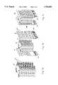
- the DIP packages 50may be combined into a DIP package assembly.
- a high capacity memory modulecomposed of nine memory packages may be assembled.
- nine packages 50are assembled into a stack using the snap fasteners 70 on their walls so as to align the leads 52 of each package 50 with respect to the leads 52 of other packages.
- the leads 52 projecting from both edges of the nine-package stackare inserted into a pair of through-hole printed circuit (PC) boards 80 having holes 82 arranged so as to accommodate the leads 52.
- PCprinted circuit
- Printed conductorsare formed on the PC boards 80 to interconnect the holes 82 so as to provide a prescribed connection between the leads 52 of the packages 50 in the IC module.
- the PC boards 80may be provided with leads 84 projecting from one edge of each PC board.
- the inserted leads 52are soldered to the PC boards 80 to produce a DIP package assembly 90.
- the leads 84 of the PC boards 80may be inserted into a motherboard that carries the external conductors to be connected with the inner circuits of the package assembly 90, and soldered to the motherboard.
- FIGS. 7A-7Cillustrate a set composed of nine DIP packages, it is to be understood that any number of the packages 50 can be attached to each other.
- Each packageis provided with locking elements of snap fasteners that allow several packages to be assembled into a stack so as to align the leads of each packet with respect to the leads of the other packages.
- the leads projecting from both edges of the stack package assemblyare inserted into a pair of PC boards having holes arranged so as to accommodate the leads of the assembly.
- the leads of the PC boardsmay be inserted into a motherboard that carries the external conductors to be connected with the inner circuits of the package assembly.
- the high density DIP package assemblycan be provided that is low in cost and can be easily implemented.
- the DIP package assembly of the present inventionhas short conductors for interconnecting packages in the assembly.
- parasitic inductance and capacitancecan be reduced compared to conventional PCB-based DIP package assemblies, and the speed of operation can be increased.
Landscapes
- Engineering & Computer Science (AREA)
- Microelectronics & Electronic Packaging (AREA)
- Power Engineering (AREA)
- Physics & Mathematics (AREA)
- Condensed Matter Physics & Semiconductors (AREA)
- General Physics & Mathematics (AREA)
- Computer Hardware Design (AREA)
- Combinations Of Printed Boards (AREA)
Abstract
Description
Claims (8)
Priority Applications (1)
| Application Number | Priority Date | Filing Date | Title |
|---|---|---|---|
| US08/559,872US5754405A (en) | 1995-11-20 | 1995-11-20 | Stacked dual in-line package assembly |
Applications Claiming Priority (1)
| Application Number | Priority Date | Filing Date | Title |
|---|---|---|---|
| US08/559,872US5754405A (en) | 1995-11-20 | 1995-11-20 | Stacked dual in-line package assembly |
Publications (1)
| Publication Number | Publication Date |
|---|---|
| US5754405Atrue US5754405A (en) | 1998-05-19 |
Family
ID=24235406
Family Applications (1)
| Application Number | Title | Priority Date | Filing Date |
|---|---|---|---|
| US08/559,872Expired - Fee RelatedUS5754405A (en) | 1995-11-20 | 1995-11-20 | Stacked dual in-line package assembly |
Country Status (1)
| Country | Link |
|---|---|
| US (1) | US5754405A (en) |
Cited By (25)
| Publication number | Priority date | Publication date | Assignee | Title |
|---|---|---|---|---|
| US5936840A (en)* | 1997-11-03 | 1999-08-10 | Texas Instruments Incorporated | Stacked passive components |
| USD420983S (en)* | 1998-10-16 | 2000-02-22 | Ixys Corporation | Semiconductor power package with three leads |
| US6163459A (en)* | 1997-07-25 | 2000-12-19 | Matsushita Electric Industrial Co., Ltd. | Semiconductor mounting system and semiconductor chip |
| US6201698B1 (en)* | 1998-03-09 | 2001-03-13 | California Institute Of Technology | Modular electronics packaging system |
| US6281577B1 (en)* | 1996-06-28 | 2001-08-28 | Pac Tech-Packaging Technologies Gmbh | Chips arranged in plurality of planes and electrically connected to one another |
| US6288907B1 (en)* | 1996-05-20 | 2001-09-11 | Staktek Group, L.P. | High density integrated circuit module with complex electrical interconnect rails having electrical interconnect strain relief |
| US6324071B2 (en)* | 1999-01-14 | 2001-11-27 | Micron Technology, Inc. | Stacked printed circuit board memory module |
| US6456496B1 (en)* | 2000-10-30 | 2002-09-24 | 3Com Corporation | Type III pccard system with full wall modular extendable RJ45/11 connector |
| US6456502B1 (en)* | 1998-09-21 | 2002-09-24 | Compaq Computer Corporation | Integrated circuit device/circuit board connection apparatus |
| US6542376B1 (en)* | 2001-03-30 | 2003-04-01 | L-3 Communications Corporation | High density packaging of electronic components |
| US20030137059A1 (en)* | 2002-01-22 | 2003-07-24 | Honeywell International Inc. | High density 3-D integrated circuit package |
| US20030231477A1 (en)* | 2002-04-12 | 2003-12-18 | Avx Corporation | Discrete component array |
| US6683373B1 (en)* | 1999-08-02 | 2004-01-27 | Alcatel | Method of modifying connecting leads and thinning bases of encapsulated modular electronic components to obtain a high-density module, and a module obtained thereby |
| US6686654B2 (en)* | 2001-08-31 | 2004-02-03 | Micron Technology, Inc. | Multiple chip stack structure and cooling system |
| US20040207061A1 (en)* | 2001-08-30 | 2004-10-21 | Farrar Paul A. | Multi-chip electronic package and cooling system |
| US6856029B1 (en)* | 2001-06-22 | 2005-02-15 | Lsi Logic Corporation | Process independent alignment marks |
| US20050121763A1 (en)* | 2003-11-14 | 2005-06-09 | Ucok Asli B. | Multi-substrate package and method for assembling same |
| US20050161794A1 (en)* | 2001-03-30 | 2005-07-28 | Fujitsu Limited | Semiconductor device, method for manufacturing the semiconductor device and semiconductor substrate |
| US20060170090A1 (en)* | 2005-01-31 | 2006-08-03 | Spansion Llc | Stacked type semiconductor device and method of fabricating stacked type semiconductor device |
| US7098073B1 (en) | 2005-04-18 | 2006-08-29 | Freescale Semiconductor, Inc. | Method for stacking an integrated circuit on another integrated circuit |
| US20060231938A1 (en)* | 2005-04-18 | 2006-10-19 | Mangrum Marc A | Structure for stacking an integrated circuit on another integrated circuit |
| US7298625B1 (en)* | 2007-01-17 | 2007-11-20 | Inventec Corporation | Expansion structure of memory module slot |
| US7465608B1 (en) | 2001-08-17 | 2008-12-16 | Micron Technology, Inc. | Three-dimensional multichip module |
| US9413114B2 (en)* | 2013-06-10 | 2016-08-09 | Semikron Elektronik Gmbh & Co., Kg | Three-level power converter |
| DE102014108641B4 (en)* | 2013-06-25 | 2020-03-26 | Infineon Technologies Ag | CIRCUIT ARRANGEMENT AND METHOD FOR PRODUCING THE SAME |
Citations (25)
| Publication number | Priority date | Publication date | Assignee | Title |
|---|---|---|---|---|
| US3515949A (en)* | 1967-11-22 | 1970-06-02 | Bunker Ramo | 3-d flatpack module packaging technique |
| US3671812A (en)* | 1970-07-01 | 1972-06-20 | Martin Marietta Corp | High density packaging of electronic components in three-dimensional modules |
| JPS60263448A (en)* | 1984-06-11 | 1985-12-26 | Mitsubishi Electric Corp | Plastic IC package |
| US4718858A (en)* | 1986-06-16 | 1988-01-12 | Western Digital Corporation | Mechanical interconnect system for electronic units enclosed in stackable housings |
| US4734825A (en)* | 1986-09-05 | 1988-03-29 | Motorola Inc. | Integrated circuit stackable package |
| US4922381A (en)* | 1986-03-25 | 1990-05-01 | Hughes Aircraft Company | Stacked circuit cards and guided configurations |
| JPH02260448A (en)* | 1989-03-30 | 1990-10-23 | Mitsubishi Electric Corp | Semiconductor device and radiating fin |
| JPH0332050A (en)* | 1989-06-28 | 1991-02-12 | Mitsubishi Electric Corp | IC package |
| JPH0396266A (en)* | 1989-09-08 | 1991-04-22 | Mitsubishi Electric Corp | Semiconductor integrated circuit module |
| US5105261A (en)* | 1989-03-30 | 1992-04-14 | Mitsubishi Denki Kabushiki Kaisha | Semiconductor device package having particular lead structure for mounting multiple circuit boards |
| US5121299A (en)* | 1989-12-29 | 1992-06-09 | International Business Machines Corporation | Multi-level circuit structure utilizing conductive cores having conductive protrusions and cavities therein |
| JPH04209562A (en)* | 1990-12-06 | 1992-07-30 | Fujitsu Ltd | Module structure of semiconductor package |
| US5198888A (en)* | 1987-12-28 | 1993-03-30 | Hitachi, Ltd. | Semiconductor stacked device |
| US5279029A (en)* | 1990-08-01 | 1994-01-18 | Staktek Corporation | Ultra high density integrated circuit packages method |
| US5315239A (en)* | 1991-12-16 | 1994-05-24 | Hughes Aircraft Company | Circuit module connections |
| US5329418A (en)* | 1991-11-18 | 1994-07-12 | Kabushiki Kaisha Toshiba | 3-D communication and interconnect technique for increased number of computational modules in large-scale electronic equipment |
| US5329423A (en)* | 1993-04-13 | 1994-07-12 | Scholz Kenneth D | Compressive bump-and-socket interconnection scheme for integrated circuits |
| US5334875A (en)* | 1987-12-28 | 1994-08-02 | Hitachi, Ltd. | Stacked semiconductor memory device and semiconductor memory module containing the same |
| US5343075A (en)* | 1991-06-29 | 1994-08-30 | Sony Corporation | Composite stacked semiconductor device with contact plates |
| US5446313A (en)* | 1992-05-25 | 1995-08-29 | Hitachi, Ltd. | Thin type semiconductor device and module structure using the device |
| US5457071A (en)* | 1993-09-03 | 1995-10-10 | International Business Machine Corp. | Stackable vertical thin package/plastic molded lead-on-chip memory cube |
| US5514907A (en)* | 1995-03-21 | 1996-05-07 | Simple Technology Incorporated | Apparatus for stacking semiconductor chips |
| US5616962A (en)* | 1992-01-24 | 1997-04-01 | Kabushiki Kaisha Toshiba | Semiconductor integrated circuit devices having particular terminal geometry |
| US5623395A (en)* | 1995-12-15 | 1997-04-22 | Mitsubishi Semiconductor America, Inc. | Integrated circuit package assembly |
| US5625221A (en)* | 1994-03-03 | 1997-04-29 | Samsung Electronics Co., Ltd. | Semiconductor assembly for a three-dimensional integrated circuit package |
- 1995
- 1995-11-20USUS08/559,872patent/US5754405A/ennot_activeExpired - Fee Related
Patent Citations (27)
| Publication number | Priority date | Publication date | Assignee | Title |
|---|---|---|---|---|
| US3515949A (en)* | 1967-11-22 | 1970-06-02 | Bunker Ramo | 3-d flatpack module packaging technique |
| US3671812A (en)* | 1970-07-01 | 1972-06-20 | Martin Marietta Corp | High density packaging of electronic components in three-dimensional modules |
| JPS60263448A (en)* | 1984-06-11 | 1985-12-26 | Mitsubishi Electric Corp | Plastic IC package |
| US4922381A (en)* | 1986-03-25 | 1990-05-01 | Hughes Aircraft Company | Stacked circuit cards and guided configurations |
| US4718858A (en)* | 1986-06-16 | 1988-01-12 | Western Digital Corporation | Mechanical interconnect system for electronic units enclosed in stackable housings |
| US4734825A (en)* | 1986-09-05 | 1988-03-29 | Motorola Inc. | Integrated circuit stackable package |
| US5198888A (en)* | 1987-12-28 | 1993-03-30 | Hitachi, Ltd. | Semiconductor stacked device |
| US5334875A (en)* | 1987-12-28 | 1994-08-02 | Hitachi, Ltd. | Stacked semiconductor memory device and semiconductor memory module containing the same |
| JPH02260448A (en)* | 1989-03-30 | 1990-10-23 | Mitsubishi Electric Corp | Semiconductor device and radiating fin |
| US5105261A (en)* | 1989-03-30 | 1992-04-14 | Mitsubishi Denki Kabushiki Kaisha | Semiconductor device package having particular lead structure for mounting multiple circuit boards |
| US5025307A (en)* | 1989-03-30 | 1991-06-18 | Mitsubishi Denki Kabushiki Kaisha | Modular semiconductor device |
| JPH0332050A (en)* | 1989-06-28 | 1991-02-12 | Mitsubishi Electric Corp | IC package |
| JPH0396266A (en)* | 1989-09-08 | 1991-04-22 | Mitsubishi Electric Corp | Semiconductor integrated circuit module |
| US5121299A (en)* | 1989-12-29 | 1992-06-09 | International Business Machines Corporation | Multi-level circuit structure utilizing conductive cores having conductive protrusions and cavities therein |
| US5279029A (en)* | 1990-08-01 | 1994-01-18 | Staktek Corporation | Ultra high density integrated circuit packages method |
| JPH04209562A (en)* | 1990-12-06 | 1992-07-30 | Fujitsu Ltd | Module structure of semiconductor package |
| US5343075A (en)* | 1991-06-29 | 1994-08-30 | Sony Corporation | Composite stacked semiconductor device with contact plates |
| US5329418A (en)* | 1991-11-18 | 1994-07-12 | Kabushiki Kaisha Toshiba | 3-D communication and interconnect technique for increased number of computational modules in large-scale electronic equipment |
| US5315239A (en)* | 1991-12-16 | 1994-05-24 | Hughes Aircraft Company | Circuit module connections |
| US5616962A (en)* | 1992-01-24 | 1997-04-01 | Kabushiki Kaisha Toshiba | Semiconductor integrated circuit devices having particular terminal geometry |
| US5446313A (en)* | 1992-05-25 | 1995-08-29 | Hitachi, Ltd. | Thin type semiconductor device and module structure using the device |
| US5329423A (en)* | 1993-04-13 | 1994-07-12 | Scholz Kenneth D | Compressive bump-and-socket interconnection scheme for integrated circuits |
| US5543660A (en)* | 1993-09-03 | 1996-08-06 | International Business Machines Corp. | Stackable vertical thin package/plastic molded lead-on-chip memory cube |
| US5457071A (en)* | 1993-09-03 | 1995-10-10 | International Business Machine Corp. | Stackable vertical thin package/plastic molded lead-on-chip memory cube |
| US5625221A (en)* | 1994-03-03 | 1997-04-29 | Samsung Electronics Co., Ltd. | Semiconductor assembly for a three-dimensional integrated circuit package |
| US5514907A (en)* | 1995-03-21 | 1996-05-07 | Simple Technology Incorporated | Apparatus for stacking semiconductor chips |
| US5623395A (en)* | 1995-12-15 | 1997-04-22 | Mitsubishi Semiconductor America, Inc. | Integrated circuit package assembly |
Non-Patent Citations (1)
| Title |
|---|
| IBM Technical Disclosure Bulletin Stackable Plastic Semiconductor Chip Carrier by Robock vol. 27 No. 4B pp. 2389 and 2390, Sep. 1984.* |
Cited By (44)
| Publication number | Priority date | Publication date | Assignee | Title |
|---|---|---|---|---|
| US6288907B1 (en)* | 1996-05-20 | 2001-09-11 | Staktek Group, L.P. | High density integrated circuit module with complex electrical interconnect rails having electrical interconnect strain relief |
| US20020009828A1 (en)* | 1996-06-28 | 2002-01-24 | Pac Tech - Packaging Technologies Gmbh | Process for the formation of a spatial chip arrangement and spatial chip arrangement |
| US7087442B2 (en) | 1996-06-28 | 2006-08-08 | Pac Tech-Packaging Technologies Gmbh | Process for the formation of a spatial chip arrangement and spatial chip arrangement |
| US6281577B1 (en)* | 1996-06-28 | 2001-08-28 | Pac Tech-Packaging Technologies Gmbh | Chips arranged in plurality of planes and electrically connected to one another |
| US6163459A (en)* | 1997-07-25 | 2000-12-19 | Matsushita Electric Industrial Co., Ltd. | Semiconductor mounting system and semiconductor chip |
| US5936840A (en)* | 1997-11-03 | 1999-08-10 | Texas Instruments Incorporated | Stacked passive components |
| US6201698B1 (en)* | 1998-03-09 | 2001-03-13 | California Institute Of Technology | Modular electronics packaging system |
| US6456502B1 (en)* | 1998-09-21 | 2002-09-24 | Compaq Computer Corporation | Integrated circuit device/circuit board connection apparatus |
| US20040104466A1 (en)* | 1998-09-21 | 2004-06-03 | Miller Joseph P. | Integrated circuit device/circuit board connection apparatus |
| US6717821B2 (en) | 1998-09-21 | 2004-04-06 | Hewlett-Packard Development Company, Lp. | Integrated circuit device/circuit board connection apparatus |
| USD420983S (en)* | 1998-10-16 | 2000-02-22 | Ixys Corporation | Semiconductor power package with three leads |
| US6418034B1 (en)* | 1999-01-14 | 2002-07-09 | Micron Technology, Inc. | Stacked printed circuit board memory module and method of augmenting memory therein |
| US6324071B2 (en)* | 1999-01-14 | 2001-11-27 | Micron Technology, Inc. | Stacked printed circuit board memory module |
| US6683373B1 (en)* | 1999-08-02 | 2004-01-27 | Alcatel | Method of modifying connecting leads and thinning bases of encapsulated modular electronic components to obtain a high-density module, and a module obtained thereby |
| US6456496B1 (en)* | 2000-10-30 | 2002-09-24 | 3Com Corporation | Type III pccard system with full wall modular extendable RJ45/11 connector |
| US6972487B2 (en)* | 2001-03-30 | 2005-12-06 | Fujitsu Limited | Multi chip package structure having a plurality of semiconductor chips mounted in the same package |
| US20060226529A1 (en)* | 2001-03-30 | 2006-10-12 | Fujitsu Limited | Semiconductor device, method for manufacturing the semiconductor device and semiconductor substrate |
| US6542376B1 (en)* | 2001-03-30 | 2003-04-01 | L-3 Communications Corporation | High density packaging of electronic components |
| US20050161794A1 (en)* | 2001-03-30 | 2005-07-28 | Fujitsu Limited | Semiconductor device, method for manufacturing the semiconductor device and semiconductor substrate |
| US6856029B1 (en)* | 2001-06-22 | 2005-02-15 | Lsi Logic Corporation | Process independent alignment marks |
| US7465608B1 (en) | 2001-08-17 | 2008-12-16 | Micron Technology, Inc. | Three-dimensional multichip module |
| US7626252B2 (en) | 2001-08-30 | 2009-12-01 | Micron Technology, Inc. | Multi-chip electronic package and cooling system |
| US20040207061A1 (en)* | 2001-08-30 | 2004-10-21 | Farrar Paul A. | Multi-chip electronic package and cooling system |
| US6975027B2 (en) | 2001-08-30 | 2005-12-13 | Micron Technology, Inc. | Multi-chip electronic package and cooling system |
| US20060103015A1 (en)* | 2001-08-30 | 2006-05-18 | Farrar Paul A | Multi-chip electronic package and cooling system |
| US6861287B2 (en) | 2001-08-31 | 2005-03-01 | Micron Technology, Inc. | Multiple chip stack structure and cooling system |
| US20040063248A1 (en)* | 2001-08-31 | 2004-04-01 | Farrar Paul A. | Multiple chip stack structure and cooling system |
| US6686654B2 (en)* | 2001-08-31 | 2004-02-03 | Micron Technology, Inc. | Multiple chip stack structure and cooling system |
| US6958533B2 (en)* | 2002-01-22 | 2005-10-25 | Honeywell International Inc. | High density 3-D integrated circuit package |
| US20050263870A1 (en)* | 2002-01-22 | 2005-12-01 | Honeywell International Inc. | High density 3-D integrated circuit package |
| US20030137059A1 (en)* | 2002-01-22 | 2003-07-24 | Honeywell International Inc. | High density 3-D integrated circuit package |
| US7176063B2 (en) | 2002-01-22 | 2007-02-13 | Honeywell International Inc. | High density 3-D integrated circuit package |
| US7057878B2 (en) | 2002-04-12 | 2006-06-06 | Avx Corporation | Discrete component array |
| US20030231477A1 (en)* | 2002-04-12 | 2003-12-18 | Avx Corporation | Discrete component array |
| US20050121763A1 (en)* | 2003-11-14 | 2005-06-09 | Ucok Asli B. | Multi-substrate package and method for assembling same |
| US6958531B2 (en)* | 2003-11-14 | 2005-10-25 | The Regents Of The University Of Michigan | Multi-substrate package and method for assembling same |
| US20060170090A1 (en)* | 2005-01-31 | 2006-08-03 | Spansion Llc | Stacked type semiconductor device and method of fabricating stacked type semiconductor device |
| US7696616B2 (en)* | 2005-01-31 | 2010-04-13 | Spansion Llc | Stacked type semiconductor device and method of fabricating stacked type semiconductor device |
| US20060231938A1 (en)* | 2005-04-18 | 2006-10-19 | Mangrum Marc A | Structure for stacking an integrated circuit on another integrated circuit |
| US7098073B1 (en) | 2005-04-18 | 2006-08-29 | Freescale Semiconductor, Inc. | Method for stacking an integrated circuit on another integrated circuit |
| US7196427B2 (en) | 2005-04-18 | 2007-03-27 | Freescale Semiconductor, Inc. | Structure having an integrated circuit on another integrated circuit with an intervening bent adhesive element |
| US7298625B1 (en)* | 2007-01-17 | 2007-11-20 | Inventec Corporation | Expansion structure of memory module slot |
| US9413114B2 (en)* | 2013-06-10 | 2016-08-09 | Semikron Elektronik Gmbh & Co., Kg | Three-level power converter |
| DE102014108641B4 (en)* | 2013-06-25 | 2020-03-26 | Infineon Technologies Ag | CIRCUIT ARRANGEMENT AND METHOD FOR PRODUCING THE SAME |
Similar Documents
| Publication | Publication Date | Title |
|---|---|---|
| US5754405A (en) | Stacked dual in-line package assembly | |
| US5754408A (en) | Stackable double-density integrated circuit assemblies | |
| US6168469B1 (en) | Electrical connector assembly and method for making the same | |
| US6493240B2 (en) | Interposer for connecting two substrates and resulting assembly | |
| US5994648A (en) | Three-dimensional molded sockets for mechanical and electrical component attachment | |
| US5613033A (en) | Laminated module for stacking integrated circuits | |
| US5424492A (en) | Optimal PCB routing methodology for high I/O density interconnect devices | |
| US3815077A (en) | Electrical connector assembly | |
| US6246016B1 (en) | Edge-mountable integrated circuit package and method of attaching the same to a printed wiring board | |
| KR930024134A (en) | Multilayer semiconductor multi-chip module and manufacturing method thereof | |
| US5790381A (en) | Integrated circuit package assembly | |
| US4882656A (en) | Surface mounted decoupling capacitor | |
| US4779164A (en) | Surface mounted decoupling capacitor | |
| US6547597B2 (en) | Apparatus and method for incorporating surface mount components into connectors | |
| JPH09289052A (en) | Packaged structure of module | |
| US6739912B2 (en) | Modular jack assembly having improved positioning means | |
| US5623395A (en) | Integrated circuit package assembly | |
| US20090053919A1 (en) | Connector mounting structure | |
| US6512293B1 (en) | Mechanically interlocking ball grid array packages and method of making | |
| US4702706A (en) | Electrical connecting device including socket therefor | |
| US5644473A (en) | Carriers for IC packages | |
| US3405324A (en) | Ultracompact modular structure for low cost mounting and interconnection of electronic components | |
| US6045371A (en) | Connector for electrical connection of circuit boards and such a method for electrical connection of circuit boards using such a connector | |
| US6815614B1 (en) | Arrangement for co-planar vertical surface mounting of subassemblies on a mother board | |
| US11503732B1 (en) | Socket alignment and retention system |
Legal Events
| Date | Code | Title | Description |
|---|---|---|---|
| AS | Assignment | Owner name:MITSUBISHI SEMICONDUCTOR AMERICA, INC., NORTH CARO Free format text:ASSIGNMENT OF ASSIGNORS INTEREST;ASSIGNOR:DEROUICHE, NOUR EDDINE;REEL/FRAME:007790/0745 Effective date:19951110 | |
| FEPP | Fee payment procedure | Free format text:PAYOR NUMBER ASSIGNED (ORIGINAL EVENT CODE: ASPN); ENTITY STATUS OF PATENT OWNER: LARGE ENTITY Free format text:PAYER NUMBER DE-ASSIGNED (ORIGINAL EVENT CODE: RMPN); ENTITY STATUS OF PATENT OWNER: LARGE ENTITY | |
| AS | Assignment | Owner name:MITSUBISHI ELECTRIC CORPORATION, JAPAN Free format text:ASSIGNMENT OF ASSIGNORS INTEREST;ASSIGNOR:MITSUBISHI SEMICONDUCTOR AMERICA, INC.;REEL/FRAME:009958/0188 Effective date:19981211 | |
| FPAY | Fee payment | Year of fee payment:4 | |
| FPAY | Fee payment | Year of fee payment:8 | |
| REMI | Maintenance fee reminder mailed | ||
| LAPS | Lapse for failure to pay maintenance fees | ||
| STCH | Information on status: patent discontinuation | Free format text:PATENT EXPIRED DUE TO NONPAYMENT OF MAINTENANCE FEES UNDER 37 CFR 1.362 | |
| FP | Lapsed due to failure to pay maintenance fee | Effective date:20100519 |