US5745837A - Apparatus and method for digital data transmission over a CATV system using an ATM transport protocol and SCDMA - Google Patents
Apparatus and method for digital data transmission over a CATV system using an ATM transport protocol and SCDMADownload PDFInfo
- Publication number
- US5745837A US5745837AUS08/616,071US61607196AUS5745837AUS 5745837 AUS5745837 AUS 5745837AUS 61607196 AUS61607196 AUS 61607196AUS 5745837 AUS5745837 AUS 5745837A
- Authority
- US
- United States
- Prior art keywords
- data
- cpe
- destination
- atm cell
- atm
- Prior art date
- Legal status (The legal status is an assumption and is not a legal conclusion. Google has not performed a legal analysis and makes no representation as to the accuracy of the status listed.)
- Expired - Lifetime
Links
Images


Classifications
- H—ELECTRICITY
- H04—ELECTRIC COMMUNICATION TECHNIQUE
- H04B—TRANSMISSION
- H04B1/00—Details of transmission systems, not covered by a single one of groups H04B3/00 - H04B13/00; Details of transmission systems not characterised by the medium used for transmission
- H04B1/69—Spread spectrum techniques
- H04B1/707—Spread spectrum techniques using direct sequence modulation
- H—ELECTRICITY
- H04—ELECTRIC COMMUNICATION TECHNIQUE
- H04J—MULTIPLEX COMMUNICATION
- H04J13/00—Code division multiplex systems
- H—ELECTRICITY
- H04—ELECTRIC COMMUNICATION TECHNIQUE
- H04J—MULTIPLEX COMMUNICATION
- H04J13/00—Code division multiplex systems
- H04J13/0007—Code type
- H04J13/004—Orthogonal
- H—ELECTRICITY
- H04—ELECTRIC COMMUNICATION TECHNIQUE
- H04J—MULTIPLEX COMMUNICATION
- H04J13/00—Code division multiplex systems
- H04J13/16—Code allocation
- H04J13/18—Allocation of orthogonal codes
- H—ELECTRICITY
- H04—ELECTRIC COMMUNICATION TECHNIQUE
- H04J—MULTIPLEX COMMUNICATION
- H04J3/00—Time-division multiplex systems
- H04J3/02—Details
- H04J3/06—Synchronising arrangements
- H04J3/0635—Clock or time synchronisation in a network
- H04J3/0638—Clock or time synchronisation among nodes; Internode synchronisation
- H04J3/0652—Synchronisation among time division multiple access [TDMA] nodes, e.g. time triggered protocol [TTP]
- H—ELECTRICITY
- H04—ELECTRIC COMMUNICATION TECHNIQUE
- H04J—MULTIPLEX COMMUNICATION
- H04J3/00—Time-division multiplex systems
- H04J3/02—Details
- H04J3/06—Synchronising arrangements
- H04J3/0635—Clock or time synchronisation in a network
- H04J3/0682—Clock or time synchronisation in a network by delay compensation, e.g. by compensation of propagation delay or variations thereof, by ranging
- H—ELECTRICITY
- H04—ELECTRIC COMMUNICATION TECHNIQUE
- H04L—TRANSMISSION OF DIGITAL INFORMATION, e.g. TELEGRAPHIC COMMUNICATION
- H04L12/00—Data switching networks
- H04L12/28—Data switching networks characterised by path configuration, e.g. LAN [Local Area Networks] or WAN [Wide Area Networks]
- H04L12/2801—Broadband local area networks
- H—ELECTRICITY
- H04—ELECTRIC COMMUNICATION TECHNIQUE
- H04L—TRANSMISSION OF DIGITAL INFORMATION, e.g. TELEGRAPHIC COMMUNICATION
- H04L25/00—Baseband systems
- H04L25/02—Details ; arrangements for supplying electrical power along data transmission lines
- H04L25/03—Shaping networks in transmitter or receiver, e.g. adaptive shaping networks
- H04L25/03006—Arrangements for removing intersymbol interference
- H04L25/03343—Arrangements at the transmitter end
- H—ELECTRICITY
- H04—ELECTRIC COMMUNICATION TECHNIQUE
- H04L—TRANSMISSION OF DIGITAL INFORMATION, e.g. TELEGRAPHIC COMMUNICATION
- H04L27/00—Modulated-carrier systems
- H04L27/32—Carrier systems characterised by combinations of two or more of the types covered by groups H04L27/02, H04L27/10, H04L27/18 or H04L27/26
- H04L27/34—Amplitude- and phase-modulated carrier systems, e.g. quadrature-amplitude modulated carrier systems
- H04L27/36—Modulator circuits; Transmitter circuits
- H04L27/362—Modulation using more than one carrier, e.g. with quadrature carriers, separately amplitude modulated
- H—ELECTRICITY
- H04—ELECTRIC COMMUNICATION TECHNIQUE
- H04L—TRANSMISSION OF DIGITAL INFORMATION, e.g. TELEGRAPHIC COMMUNICATION
- H04L5/00—Arrangements affording multiple use of the transmission path
- H04L5/02—Channels characterised by the type of signal
- H04L5/023—Multiplexing of multicarrier modulation signals, e.g. multi-user orthogonal frequency division multiple access [OFDMA]
- H04L5/026—Multiplexing of multicarrier modulation signals, e.g. multi-user orthogonal frequency division multiple access [OFDMA] using code division
- H—ELECTRICITY
- H04—ELECTRIC COMMUNICATION TECHNIQUE
- H04L—TRANSMISSION OF DIGITAL INFORMATION, e.g. TELEGRAPHIC COMMUNICATION
- H04L5/00—Arrangements affording multiple use of the transmission path
- H04L5/02—Channels characterised by the type of signal
- H04L5/06—Channels characterised by the type of signal the signals being represented by different frequencies
- H—ELECTRICITY
- H04—ELECTRIC COMMUNICATION TECHNIQUE
- H04L—TRANSMISSION OF DIGITAL INFORMATION, e.g. TELEGRAPHIC COMMUNICATION
- H04L7/00—Arrangements for synchronising receiver with transmitter
- H04L7/04—Speed or phase control by synchronisation signals
- H—ELECTRICITY
- H04—ELECTRIC COMMUNICATION TECHNIQUE
- H04N—PICTORIAL COMMUNICATION, e.g. TELEVISION
- H04N7/00—Television systems
- H04N7/10—Adaptations for transmission by electrical cable
- H—ELECTRICITY
- H04—ELECTRIC COMMUNICATION TECHNIQUE
- H04N—PICTORIAL COMMUNICATION, e.g. TELEVISION
- H04N7/00—Television systems
- H04N7/16—Analogue secrecy systems; Analogue subscription systems
- H04N7/173—Analogue secrecy systems; Analogue subscription systems with two-way working, e.g. subscriber sending a programme selection signal
- H04N7/17309—Transmission or handling of upstream communications
- H—ELECTRICITY
- H04—ELECTRIC COMMUNICATION TECHNIQUE
- H04W—WIRELESS COMMUNICATION NETWORKS
- H04W48/00—Access restriction; Network selection; Access point selection
- H04W48/16—Discovering, processing access restriction or access information
- H—ELECTRICITY
- H04—ELECTRIC COMMUNICATION TECHNIQUE
- H04B—TRANSMISSION
- H04B2201/00—Indexing scheme relating to details of transmission systems not covered by a single group of H04B3/00 - H04B13/00
- H04B2201/69—Orthogonal indexing scheme relating to spread spectrum techniques in general
- H04B2201/707—Orthogonal indexing scheme relating to spread spectrum techniques in general relating to direct sequence modulation
- H04B2201/7097—Direct sequence modulation interference
- H04B2201/709709—Methods of preventing interference
- H—ELECTRICITY
- H04—ELECTRIC COMMUNICATION TECHNIQUE
- H04B—TRANSMISSION
- H04B7/00—Radio transmission systems, i.e. using radiation field
- H04B7/24—Radio transmission systems, i.e. using radiation field for communication between two or more posts
- H04B7/26—Radio transmission systems, i.e. using radiation field for communication between two or more posts at least one of which is mobile
- H04B7/2662—Arrangements for Wireless System Synchronisation
- H04B7/2668—Arrangements for Wireless Code-Division Multiple Access [CDMA] System Synchronisation
- H—ELECTRICITY
- H04—ELECTRIC COMMUNICATION TECHNIQUE
- H04H—BROADCAST COMMUNICATION
- H04H60/00—Arrangements for broadcast applications with a direct linking to broadcast information or broadcast space-time; Broadcast-related systems
- H04H60/76—Arrangements characterised by transmission systems other than for broadcast, e.g. the Internet
- H04H60/81—Arrangements characterised by transmission systems other than for broadcast, e.g. the Internet characterised by the transmission system itself
- H04H60/93—Wired transmission systems
- H04H60/96—CATV systems
- H04H60/97—CATV systems using uplink of the CATV systems
- H—ELECTRICITY
- H04—ELECTRIC COMMUNICATION TECHNIQUE
- H04J—MULTIPLEX COMMUNICATION
- H04J14/00—Optical multiplex systems
- H04J14/005—Optical Code Multiplex
- H04J14/007—Orthogonal Optical Code Multiplex
- H—ELECTRICITY
- H04—ELECTRIC COMMUNICATION TECHNIQUE
- H04J—MULTIPLEX COMMUNICATION
- H04J3/00—Time-division multiplex systems
- H04J3/02—Details
- H04J3/06—Synchronising arrangements
- H04J3/0635—Clock or time synchronisation in a network
- H04J3/0685—Clock or time synchronisation in a node; Intranode synchronisation
- H04J3/0694—Synchronisation in a TDMA node, e.g. TTP
- H—ELECTRICITY
- H04—ELECTRIC COMMUNICATION TECHNIQUE
- H04L—TRANSMISSION OF DIGITAL INFORMATION, e.g. TELEGRAPHIC COMMUNICATION
- H04L25/00—Baseband systems
- H04L25/02—Details ; arrangements for supplying electrical power along data transmission lines
- H04L25/03—Shaping networks in transmitter or receiver, e.g. adaptive shaping networks
- H04L25/03006—Arrangements for removing intersymbol interference
- H04L2025/0335—Arrangements for removing intersymbol interference characterised by the type of transmission
- H04L2025/03375—Passband transmission
- H04L2025/03414—Multicarrier
- H—ELECTRICITY
- H04—ELECTRIC COMMUNICATION TECHNIQUE
- H04L—TRANSMISSION OF DIGITAL INFORMATION, e.g. TELEGRAPHIC COMMUNICATION
- H04L7/00—Arrangements for synchronising receiver with transmitter
- H04L7/04—Speed or phase control by synchronisation signals
- H04L7/041—Speed or phase control by synchronisation signals using special codes as synchronising signal
- H—ELECTRICITY
- H04—ELECTRIC COMMUNICATION TECHNIQUE
- H04W—WIRELESS COMMUNICATION NETWORKS
- H04W28/00—Network traffic management; Network resource management
- H04W28/16—Central resource management; Negotiation of resources or communication parameters, e.g. negotiating bandwidth or QoS [Quality of Service]
- H04W28/24—Negotiating SLA [Service Level Agreement]; Negotiating QoS [Quality of Service]
- H—ELECTRICITY
- H04—ELECTRIC COMMUNICATION TECHNIQUE
- H04W—WIRELESS COMMUNICATION NETWORKS
- H04W28/00—Network traffic management; Network resource management
- H04W28/16—Central resource management; Negotiation of resources or communication parameters, e.g. negotiating bandwidth or QoS [Quality of Service]
- H04W28/26—Resource reservation
- H—ELECTRICITY
- H04—ELECTRIC COMMUNICATION TECHNIQUE
- H04W—WIRELESS COMMUNICATION NETWORKS
- H04W4/00—Services specially adapted for wireless communication networks; Facilities therefor
- H04W4/18—Information format or content conversion, e.g. adaptation by the network of the transmitted or received information for the purpose of wireless delivery to users or terminals
- H—ELECTRICITY
- H04—ELECTRIC COMMUNICATION TECHNIQUE
- H04W—WIRELESS COMMUNICATION NETWORKS
- H04W74/00—Wireless channel access
- H04W74/08—Non-scheduled access, e.g. ALOHA
- H04W74/0866—Non-scheduled access, e.g. ALOHA using a dedicated channel for access
Definitions
- the inventionpertains to the field of bidirectional communication of digital data over coaxial cable or other transmission media using an ATM protocol. More particularly, the invention pertains to the field of provision of multiple channels of digital data including interactive TV services, digital telephony, video teleconferencing, video on demand, internet access at 10 megabit/second or media data rates etc., all provided to home or business establishments over cable TV coax or combinations of coaxial cable, fiber optic links, microwave or satellite links or other wireless systems using synchronous CDMA multiplexing and ATM transport protocol.
- Cable networkstypically involve a so-called head end or central unit from which video is transmitted to subscribers coupled to one or more main trunk lines from which extend numerous branch lines which may enter subscriber homes or which may couple to other branch lines.
- a directional couplerwhich is intended to direct transmissions from the head end to the subscribers in one direction and to direct transmissions from the subscribers back to the head end without leaking energy intended for transmission to the head end into branch lines coupled to other subscribers.
- a modemis necessary at both the head end and at all the subscriber locations to modulate digital data onto the coax as RF signals, and to receive RF signals carrying digital data and derive the digital data therefrom. Because RF signals are propagating along the cables, and because the couplers are not perfect, reflections occur at the directional couplers that cause noise and interference.
- the signals from each subscriber's modemarrive at the head end at different times because of different propagation delays. Because digital data is transmitted in frames and because all subscribers must be synchronized to the same frame timing, these different propagation delays for each subscriber cause problems in synchronizing data.
- Each amplifierhas two channels, one of which amplifies signals in a high frequency range from 45-750 mHz for transmission of data from the head end to subscribers, and the other of which amplifies signals in a low frequency range from 5-42 mHz for transmission of data from the subscribers to the head end.
- Interactive systemstypically involve in excess of one hundred different channels on which separate digital data streams can flow in addition to the separate channels on which the video signals are provided for normal cable TV service.
- To send digital data as RF signalsvery complex constellations of separate amplitude and phase combinations are used to encode the digital characters being transmitted. Because of the large number of data points, the differences in phase and amplitude between the different points are not large. Therefore, the impairments described above can cause errors by causing misinterpretation by demodulators of what characters were actually sent.
- TCP/IP protocolused on the internet. This protocol is not satisfactory for provision of high demand services such as video teleconferencing and video on demand since TCP/IP has no provision to guarantee quality of service and provide guaranteed bandwidth capacity. Because there is no concept of reservation of bandwidth in TCP/IP protocol, it is not suitable for delivery simultaneously of audio, video and data services to multiple subscribers.
- the ATM protocolis the currently favored local area network protocol which is designed to simultaneously deliver integrated voice, video and data services. However, the ATM protocol was designed for local area networks where there is no shared media which is used to simultaneously deliver ATM cells between more than one pair of communicating devices.
- ATMis a point to point communication protocol that cannot be directly used on a CATV plant with its point to multipoint/multipoint to point topology.
- a method and apparatus for carrying an ATM communication protocol on a hybrid fiber coax CATV systemPoint to point communication is supported by use of synchronous code division multiplexing on the physical and by assigning on the MAC layer one or more orthogonal SCDMA codes exclusively for use by pairs of devices needing to communicate such as the head end and any customer premises equipment.
- This control of the code spaceallows virtual point to point links to be established in the physical point to multipoint environment of the CATV HFC cable plant thereby allowing effective implementation of the ATM protocols.
- the virtual link structureis coded in a two byte header containing the virtual link ID of the virtual link to which each cell belongs. This virtual link header is attached to the front end of each ATM cell's regular header. This virtual header also makes possible broadcast and multicast of packets from the head end to all CPEs for management and control purposes in resolving contentions on shared access channels, distributing code allocation (also called timeslot allocation) decisions and other management functions.
- ATM Quality of Service guarantees or guaranteed bandwidth availabilityis implemented by controlling the code space at the MAC layer such that one or more SCDMA spreading codes can be reserved to certain CPEs needing guaranteed bandwidth.
- these CPEsmay reserve one or more SCDMA codes for use exclusively by them such that virtual links are reserved exclusively to them to support the peripherals needing guaranteed bandwidth.
- ATM cell boundary synchronizationis achieved using a 9th bit on each 8-bit byte in each ATM cell.
- each byte in each ATM cellhas 8 bits of data and a 9th bit which is encoded with data to indicate where the ATM cell starts and includes CRC data for error detection and correction on the payload data in the cell.
- Bandwidthis allocated by the head end computer which executes algorithms on the MAC layer to collect actual bandwidth usage information and requests for bandwidth as well as recommendations to add to or take away bandwidth from CPEs having actual usage which does not justify the amount of bandwidth they are currently allocated. These factors are prioritized and arbitrated based upon a number of factors and based upon the channel allocation/reservation scheme currently use. The channel allocation/reservation scheme can be changed on the fly between reservation, first-come, first-serve, fixed or any combination of these methodologies.
- Reallocation calculations to adjust bandwidth allocationsare calculated every 10 milliseconds and the new allocations are distributed in downstream messages which are transmitted to all CPEs.
- Bandwidth allocationis done with a zero overhead algorithm in that, other than access requests, the CPEs need generate no upstream communications to aid in the adaptive algorithm to reallocate bandwidth.
- the head end computermeasures actual usage by each CPE by counting cells directed to and coming from each CPE using the virtual link information and compares this information to the actual bandwidth allocated to each CPE to generate suggestions to the adaptive allocation process for redistributing bandwidth on each calculation.
- a physical layerimplementing synchronous code division multiplexing multiple access (SCDMA) scheme using orthogonal codes to encode the digital data being transmitted.
- SCDMAsynchronous code division multiplexing multiple access
- the ranging/alignment scheme disclosed hereinis useful for any other modulation scheme which transmits digital data in frames, requires frame synchronization and can insert a guardband in each frame.
- SCDMAallows byte wide interleaving of bytes from multiple CPEs with very low overhead to allow multiple CPEs to simultaneously communicate with devices and networks coupled to the head end.
- a single byteis basically the lowest packet size. Although single bytes from different CPEs can be transmitted in each SCDMA frame, the amount of overhead data necessary to transmit necessary to accomplish this is very small. In other words, because the network is fully synchronized with frame boundaries determined in the ranging process and code assignments send in the downstream data, no header is needed for transmission of each byte.
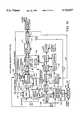
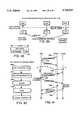
- FIG. 1is a block diagram of the functional elements needed for simultaneous transmission of digital data from multiple subscribers to a head end receiver over a shared coaxial cable using orthogonal codes and for recovery of the separate data streams from each subscriber at the head end receiver.
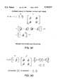
- FIG. 2is the mathematical relationship that defines the property of orthogonality of the codes used by the modulator/transmitters in FIG. 1.
- FIG. 3Ais the mathematical relationship that the system of FIG. 1 uses to recover the individual data streams sent by the subscribers at the head end and vice versa
- FIGS. 3B through 3Gillustrate a specific working example of how the mathematical relationship of FIG. 3A could be used to transmit two channels of data simultaneously over the same shared media.
- FIG. 4Ashows a typical data structure for a frame.
- FIG. 4Bis a symbolic diagram illustrating the concepts involved in alignment.
- FIG. 5is a diagram like that of FIG. 4B which illustrates a problem which occurs when the network physically expands.
- FIG. 6is a diagram like that of FIG. 5 which illustrates the solution to the misalignment problem outlined in the discussion of FIG. 5.
- FIG. 7,which is comprised of FIGS. 7A, 7B, and 7C, is a flow chart for the general alignment process which is used in training all RUs to set their delay vectors properly so as to be in alignment within the same frame.
- FIG. 8is a flow chart of one embodiment of a process to resynchronize all RUs after the CU has changed its delay vector.
- FIG. 9represents the preferred process for resychronizing all RUs after the CU has changed its delay vector.
- FIG. 10shows a typical cable television system arrangement in which the teachings of the invention find utility in a multi-RU, multichannel environment.
- FIG. 11is a block diagram of one multichannel embodiment for the internal structure of each RU modem's transmit channel circuitry for transmitting data to the CU.
- FIG. 12shows the circuitry that implements the framer in the preferred embodiment.
- FIG. 13shows the timing relationships between the chip clock signal which sets timing in the code domain and the bit and byte clocks which set timing in the time domain.
- FIG. 13also shows a number of other signals generated by time base generator 350 in FIG. 12.
- FIG. 14is a memory filling diagram that illustrates how entire 9-bit bytes are received continuously, but 3 bit tribits for each of 128 data channels are sent out simultaneously to compose the symbols of each frame.
- FIG. 15is a diagram illustrating in block diagram form how the delay necessary in each RU and CU to maintain frame synchronization system-wide is achieved.
- FIG. 16represents portions of memory 300 with the stippled portion representing the number of addresses difference between the position of the read pointer and the position of the write pointer to implement the delay.
- FIG. 17is a timing diagram showing the relative rates of incrementation of the read and write pointers in the framer.
- FIG. 18is a block diagram of the time base generator.
- FIG. 19is a block diagram of the preferred embodiment of the transceiver circuitry included in each RU and CU.
- FIG. 20is a diagram which helps illustrate the manner in which framer memory 300 is emptied for transmission.
- FIG. 21maps each of 16 possible input points, i.e., permutations of the 4 bits in each symbol array to a point in space defined by the in-phase or I axis for the real part and the quadrature or Q axis for the imaginary part of each point.
- FIG. 22is a table listing all the possible 16 combinations of 4 bits in the Code column and the corresponding 2's complement digital representation of the real and imaginary coordinates for each combination in the inphase and Quadrature columns, respectively.
- FIG. 23is an illustration of the matrix multiplication process carried out in encoder 402 in FIG. 19 to encode each symbol using an orthogonal code matrix.
- FIG. 24is a block diagram illustrating more details of the components and operation of the multiplexer 408 and the modulator 410.
- FIG. 25which is a plot of the changes in amplitude over time of the real components of the results vector for the array 409.
- FIG. 26is a more detailed diagram of the structure of the demodulator in the receive channel.
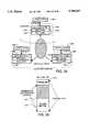
- FIG. 27is a block diagram of the basic functional blocks needed at the head end and one CPE to carry out ATM protocol communication using virtual links on a CATV HFC cable plant.
- FIG. 28is a symbolic diagram of a typical CATV HFC.
- FIG. 29is a diagram of how virtual links look at the logical level despite the physical media structure shown in FIG. 28.
- FIG. 30is a diagram illustrating the downstream data structure.
- FIG. 31is a diagram illustrating a Utopia+format 55 byte ATM cell as is used in the downstream data and illustrating how a 9th bit is added for use in signalling the beginning of each ATM cell and to carry CRC data.
- FIG. 32is a diagram illustrating how the bytes from one upstream ATM cell from one CPE are interleaved into the frames with bytes from other CPEs in accordance with a hypothetical code allocation of codes 1, 5 and 35 for one CPE.
- FIG. 33is a diagram illustrating the various layers of the OSI model and illustrating what jobs/protocols are done on each layer by the system of the invention.
- FIG. 34is a diagram illustrating the interfaces between the upper OSI model layers at the head end and CPEs with the data link, media access control and physical layers implemented by the system of the invention including connection between these layers by the virtual network.
- FIG. 35is an illustration of the format of a Utopia+55 byte ATM cell including a two byte virtual link header enabling use of this cell in a CATV HFC plant.
- FIG. 36illustrates the SCDMA frame structure of a superframe including 4 frames separated by guardbands, each frame being 125 microseconds long and containing data from 144 timeslots.
- FIG. 37illustrates how inband management channels are fit into every frame with 128 payload data timeslots.
- FIG. 38illustrates the physical layer downstream broadcast architecture for contention resolution and channel allocation messages.
- FIG. 39illustrates the upstream multipoint to point multiple access communication architecture.
- FIG. 40illustrates the format of a typical upstream management and control message.
- FIG. 41illustrates access request collisions and contention resolution protocols.
- FIG. 42illustrates the physical layer initialization sequence.
- FIG. 43illustrates one embodiment of a dynamic bandwidth manager process carried out by the head end computer.
- FIG. 44illustrates how bandwidth allocation is dynamically altered in accordance with bandwidth actually used.
- FIG. 45comprised of FIGS. 45A, 45B and 45C, is a flow chart illustrating more details of one embodiment for the dynamic bandwidth reallocation process symbolized by block 1108 in FIG. 43.
- FIG. 46illustrates one possible structure for a table of data for use by the process of FIG. 45 in dynamically reallocating bandwidth.
- FIG. 47is a block diagram of the preferred embodiment for the multiplexer/demultiplexer ATM/SCDMA interface 1008 in FIG. 27.
- FIG. 48is a flowchart of operations by the data framer 1246.
- FIG. 49is a flowchart of the processing carried out by the cell output controller 1243 in retrieving completed ATM cells from the cell buffer memory 1254 and transferring them to the SAR.
- FIG. 50is a block diagram of the circuitry inside a formatter 1030 inside every CPE modem.
- FIG. 51is a block diagram of an optimized system according to the teachings of the invention to send data organized into ATM format cells over a CATV system bidirectionally between a head end modem and a plurality of CPE modems using SCDMA with the ATM cells optimized to have 2 byte headers in the downstream direction and 0 byte headers in the upstream direction.
- FIG. 52is a block diagram of a CPE modem having a structure designed for use with a number of peripherals coupled to the CPE modem by an Ethernet LAN.
- FIG. 53is a diagram of an optimized downstream ATM cell having a 2-byte header.
- FIG. 54is a diagram of an optimized upstream ATM cell having a 0 byte header.
- FIG. 55is a more detailed block diagram of the circuits inside blocks 1370 and 1372 in FIG. 51.
- the main teachings of the inventionpertain to how an ATM local area network protocol can be used to implement a data link and MAC layer in a CATV plant, the degree of coupling between this technology and the SCDMA physical layer is tight.
- FIGS. 1-26describe in detail how SCDMA can be used in a CATV system.
- the description of how the ATM protocol can be implemented in a CATV systemstarts with the description of FIG. 27.
- FIG. 1there is shown a conceptual diagram of a system for multiple access digital communication over a cable TV coaxial conductor distribution system using orthogonal codes for CDMA.
- the system of FIG. 1depicts only the circuitry to transmit data from multiple subscribers to a head end receiver. Similar circuitry to transmit data from the head end back to the subscribers exists but is not shown for simplicity.
- FIG. 2is the mathematical relationship that defines the property of orthogonality of the codes used by the modulator/transmitters in the system.
- the codesare different and orthogonal, the summation of the products of the signals modulated by these orthogonal codes is zero, meaning that signals modulated by the different orthogonal codes can travel over the same conductor without interference and without crosstalk.
- orthogonal codesThere is more that one set of orthogonal codes, but any orthogonal code will suffice to practice this aspect of the teachings of the invention.
- FIG. 3Ais the mathematical relationship which the system of FIG. 1 uses to send multiple channels of digital data over the same conductor without interference between channels.
- b! in FIG. 3Arepresents an information vector that contains a symbol to be transmitted on each channel as a vector element.
- c!represents a code matrix having the unique orthogonal code for each channel as its columns.
- c T !represents the transpose matrix of the code matrix c! where each column of c! becomes a row of c T !.
- i!represents the identity matrix where all entries are zeroes except for a line of 1's along the diagonal.
- the matrix multiplication b! ⁇ c!is the processing that occurs on the transmit side of each transmission.
- the processing that occurs on the receiver side of the transmissionis a matrix multiplication of the transpose matrix c T ! times the signals generated on the transmit side by the multiplication of the information vector b! times the code matrix c! to yield a matrix representing the product b! ⁇ i!. Because the identity matrix is known, the product b! ⁇ i! allows recovery of the information vector b!.
- subscriber #1provides a digital input stream of symbols or bits using any input device or computer (not shown).
- This digital data stream to be transmitted to the head endarrives on bus 10 at the data input of a code #1 modulator/transmitter 12.
- This digital data streamwill be divided into individual symbols transmitted at the rate of three symbols/frame in the preferred embodiment.
- the teachings of the inventioncan be employed using symbols, data bytes or any other grouping of digital data.
- the first bit from the stream on bus 10will be the first vector element in the information vector b!.
- symbolsare formed by filling individual address locations in a framer memory (not shown) with 9 bit bytes which arrive one per timeslot.
- the individual data streams on buses 10 and 14are TDMA streams divided into multiple successive timeslots.
- timeincreases along one axis of the framer memory.
- Symbolsare formed by reading the memory "across time", i.e., along an axis orthogonal to the axis of increasing time.
- modulator/transmitter 12converts the digital data in the data stream arriving on bus 10 into amplitude modulations of a carrier signal using a first orthogonal code, and outputs the modulated carrier signal on feeder link coaxial conductor 18 coupled to an input of a summer 20. To do this, the modulator/transmitter 12 performs a matrix multiplication of the element of the information vector b! from the TDMA stream on bus 10 times the appropriate element of the first column of code matrix c!, i.e., code #1 and uses the results to control a modulator which appropriately modulates an RF carrier. All other elements of the information vector b!
- each modulator/transmitterdoes only the portion of the matrix multiplication b! ⁇ c! for data from its TDMA stream.
- subscriber #2provides a digital data input stream on bus 14 to a code #2 modulator/transmitter 16.
- This digital data stream on bus 14will be divided into individual symbols or bits to be transmitted.
- the first bit from the stream on bus 10will become the second vector element in the information vector b!.
- Modulator/transmitter 16converts the digital data in the data stream arriving on bus 14 into amplitude modulations of a carrier signal by partial matrix multiplication similar to that done by modulator/transmitter 12 using a second code, i.e., another column of the code matrix c! which is orthogonal to said first code. Modulator/transmitter 16 then outputs the modulated carrier onto a feeder link coaxial cable 22 coupled to another input of summer 20. That is, the modulator/transmitter 16 performs the multiplication of the second element of information vector b! times the appropriate element of the second column of code matrix c!, i.e., code #2.
- the effect of the multiplications by the modulator/transmitters 12 and 16is to spread the energy of each bit or symbol to be transmitted out over time by multiplication of each bit in the information vector by the multiple code elements in the appropriate column of the code matrix c!.
- the individual bits in the TDMA streams in the time domain on buses 10 and 14are not transmitted in contiguous temporal relationship in the symbols used in the matrix multiplications to generate the signals transmitted in the code domain on coaxial/fiber data paths 18, 22 and 24.
- This form of spread spectrum modulationrenders the system less susceptible to burst or impulse noise interference that adversely affects timeslots in the TDMA streams.
- orthogonal codesprovides simultaneous multiple access such that multiple digital channels can be simultaneously transmitted over a shared data path, and minimizes crosstalk between digital channels, especially where proper frame timing alignment among multiple subscribers is utilized.
- each of the modulator/transmitters 12 and 16uses the partial results of the multiplication b! ⁇ c!, i.e., one element of the b! vector times the appropriate element of a column of the c! matrix, to modulate a carrier signal generated therein to generate the RF signals which are summed by summer 20 and transmitted to the head end receiver 26 on coaxial links 18 and 22.
- the information vector b! for the first frame of data to be transmittedis 1,-1! with the first element, 1, representing the number the first user wants to send during the first frame on channel 1, and the second element, -1, representing the number the second user wants to send during the first frame on channel #2.
- the multiplication of the information vector b! times the code matrix c!results in a result vector R for transmission of 0,2/ ⁇ 2!. This multiplication is done by multiplying information vector 1,-1! times the first column of the matrix and summing the two products 1/ ⁇ 2 and -1/ ⁇ 2 to yield 0 as the first element of the result vector.
- the modulator/transmitter 16will modulate the carrier to an amplitude or frequency representing the level 2/ ⁇ 2 of the second element of the result vector R during a second time and drives the carrier so modulated onto coaxial link 22 as the combined signal carrying the data from both channels #1 and #2 simultaneously across the shared transmission media 24.
- Shared transmission media 24can be any metallic or fiber optic media, terrestrial microwave link or satellite/cellular link.
- Appropriate interface circuitry to place the result signal represented by the vector 0,2/2 ⁇ 2! onto the particular transmission mediaare known and are not critical to the invention.
- the multiplication b! ⁇ c!is carried out by the two code modulator/transmitters 12 and 16, each doing a part of the multiplication.
- Modulator 12multiplies the first element of the information vector b! from subscriber #1 times the elements in the first row of the code matrix and outputs the resulting partial products during two successive intervals on line 18 coupled to the input of the summer 20.
- the code #2 modulator 16multiplies the second element of the information vector b! from subscriber #2 times the two elements in the second row of the code matrix c! and outputs the resulting two partial products on line 22 to the summer 20 during the same two successive intervals used by modulator 12.
- the signals output by the modulator/transmitters 12 and 16 during the second of the two successive intervalsare summed by summer 20 and output on coaxial cable 24 as the second component, 2/ ⁇ 2, of the result vector 0,2/2 ⁇ 2!.
- a modulatorthat takes the result vector and uses it to modulate the amplitude, phase or frequency (or some combination of these) of a radio frequency carrier, which is then input to the shared transmission media 24 for transmission to the head end.
- the resulting recovered information vector b!is 1,-1!.
- a normalization factorequal to the square root of the number of separate codes in use, is used on both the transmit and receive sides as a denominator for each code matrix element and as a denominator for each transpose matrix element. This enables recovery by the receivers of an information vector b! which has elements which are equal to the original data generated by the users.
- each of the elements in the code matrix c!(and, consequently, its transpose matrix c T ! ) are divided by this normalization factor ⁇ 2.
- coaxial cable 24is coupled to a head end receiver 26.
- the signal on cable 24is split onto separate coaxial cable links 28 and 30, each of which is coupled to a receiver of which receivers 32 and 38 are typical.
- the function of the receiversis to demodulate the received signals to derive the elements of the result vector which were used as modulation factors, and to multiply these result vector elements times the columns of the transpose matrix c T ! to recover the information vector b! originally transmitted.
- link 28is coupled to the analog input of a receiver 32 which is comprised of a multiplier 34 and an integrator 36.
- a demodulator/discriminatorwhich converts the amplitude, phase or frequency variations (or some combination of the two) of the incoming RF signals received from coaxial cable/fiber optic data path 24 into analog signals representing the result vector elements which are coupled to the analog inputs of the multipliers 34 and 40.
- the multiplier 34receives as one input the demodulated analog signal on link 28 and as another input on line 35 an analog signal representing the elements in column 1 of the transpose matrix c T !.
- link 30 and the demodulator/discriminator(not shown) is coupled to a receiver 38 which is comprised of a multiplier 40 and an integrator 42.
- the multiplier 40has as one input, the analog demodulated signal from link 30 and has as another input a signal on line 37 representing the elements of column 2 of the transpose matrix c T !.
- Multiplier 34multiplies the signals on link 28 during a first time interval times the first column element of the first column of the transpose matrix and outputs the result on line 44 to the summation input of integrator 36.
- the multiplier 34multiplies the second element thereof, 2/ ⁇ 2, times the second element in the first column of the transpose matrix c T ! and outputs the partial product result on line 44 to the summation input of the integrator 36.
- the integrator 36sums the two partial products from the first and second time intervals, and outputs the sum on line 46 as the first element, 1, of the recovered information vector b!.
- multiplier 40multiplies the signals on line 30 during a first time interval when the first element, 0, of the result vector 0,2/ ⁇ 2! is arriving times the first element of the second column of the transpose matrix c T ! arriving on line 37.
- the resulting partial productis output on line 48 to the input of the integrator 42.
- multiplier 40multiplies this second element times the second element of second column of the transpose matrix.
- the resulting partial product during the second time intervalis output on line 48 to the integrator 42.
- the integratorsums the two partial product results on line 48 over time, and outputs the result on line 50 as the second element, -1, of the recovered information vector b!.
- the information vector b!can then be disassembled into its components such that the TDMA data streams from which data was taken to compose the information vector can be re-created at the receiver end of the transaction.
- first and second conductorscould also be assigned to carrying two different data streams sent on different channels both of which were originated by the same subscriber.
- coaxial cablethe conductors of the distribution system have been referred to as coaxial cable.
- the various coaxial cable links described hereincould be fiber optic cable, microwave links, radio frequency links, etc. since the medium of transmission is not critical to the invention.
- the orthogonal codes used in the modulator/transmittersare cyclic codes.
- cyclic orthogonal codesall codes used are the same sequence of numbers, but each code is shifted by one or more bit positions from the preceding code.
- the cyclic orthogonal codessimplify implementation issues by reducing the amount of storage needed to store the codes.
- each subscriber transmittermay transmit multiple channels of digital data, and that the matrix multiplication and summation operations described above may be performed with digital circuitry such as suitably programmed microprocessors.
- the separate streams of digital dataare transmitted using spread spectrum frequency hopping techniques.
- a first stream of digital datawill be transmitted from one end to the other using a carrier that hops in frequency in accordance with a first predetermined coded sequence.
- the second stream of digital datais transmitted on a carrier that hops in frequency in accordance with a second predetermined sequence.
- the transmitter/modulatorsreceive code sequence inputs that control the frequency of an oscillator that generates a carrier frequency.
- the codes that control the frequency of the transmitters for the various channelsare orthogonal.
- the receiver for channel 1receives the same code sequence that was fed to the transmitter for channel 1.
- This code sequencecontrols the frequency of a local beat frequency oscillator for receiver 1 and is synchronized with the code sequence fed to the transmitter for channel 1.
- the receiver for channel 2receives a code sequence that is orthogonal to the receiver for channel 1 code sequence and controls the beat frequency oscillator of the receiver for channel 2 to synchronously generate hops in the local oscillator frequency that track the hops in the frequency of the carrier for the transmitter for channel 2.
- the time slots in the TDMA streams on lines 10 and 14are the channels.
- the digital data in each time slot in the TDMA streams on lines 10 and 14is data transmitted on that channel.
- the digital data in the TDMA streamsis re-arranged into symbols, as described briefly above, and is transmitted in frames, with three symbols plus one guard band or gap per frame.
- the guardband or gapis reserved for transmission of alignment barker codes, and no other data is supposed to be transmitted during the gaps.
- the concept in alignmentis to adjust variable delays imposed at the site of each transmitter prior to transmission of a barker code so as to compensate for different propagation delays from each transmitter site such that the barker code from each subscriber transmitter trying to align arrives at the head end receiver during the same gap.
- variable delays at each subscriber transmitterare adjusted properly, each subscriber will be said to be in alignment so that the signals encoding the symbols that are simultaneously transmitted on the shared data path 24 will all be transmitted with the same frame timing.
- Alignmentis important to obtain pure orthogonality so as to obtain zero cross talk. If the transmitters are not perfectly aligned, the signals transmitted can still be recovered, but there is some cross talk between channels which will limit the capacity of the system to carry information.
- This process of aligning all the delay circuits in the transmittersis sometimes alternatively called ranging herein and is broadly applicable to other types of multiple access digital data transmission systems also which suffer from different propagation times from different transmitter sites such as time division multiple access systems that form part of the prior art discussed above.
- FIG. 4Athere is shown a diagram of the typical frame structure.
- Each frameis composed of three symbols of 144 chips each and a gap or guardband comprised of 16 chips for a total of 448 chips each having 278 nanoseconds duration.
- the chipis the basic unit of time in the "code domain", where code domain refers to the signals propagating across the shared media.
- the three symbols of frame F nare symbolized by blocks 62, 64, and 66.
- the gap or guardbandis symbolized by blocks 60 and 71.
- the guardband 71(sometimes also referred to herein as the gap) is used for synchronization and equalization purposes for the frame comprised of symbols 62, 64, 66 and guardband 71.
- the symbolscarry the information for the various channels of digital data provided to the subscribers.
- the frame periodis 125 microseconds.
- the frame data payloadis 128 channels times 72 kilobits per second per channel plus 16 control and management channels each of which has a data rate of 72 kilobits per second for management and control information.
- each subscriber transmitterwill be referred to as a remote unit or RU, and the central unit or head end will be referred to as the CU.
- the process of synchronizationis the process wherein each RU is "trained", i.e., has a variable delay in its transmitter set using feedback from the CU on one of the management and control channels such that the transmitted frame from each RU arrives at the CU at the same time. Alignment of all frames from all RUs results in the beginning of the gap 60 for each frame from each RU occurring at the same time at the location of the CU regardless of differences in propagation delays from the various RUs to the CU. In FIG. 4A, time increases to the right. Therefore the beginning of the guardband 60 is located at point 61.
- FIG. 4Bthere is shown a symbolic diagram illustrating the concepts involved in alignment.
- points having increasing positive coordinates along the y-axis starting from the origin at 100represent increasing time.
- Points along the x-axis to the right of originrepresent increasing distance from the central unit which is designated at position 70.
- Time 100represents the beginning of symbol 62 in FIG. 4A at the CU.
- the gap 71 at the end of the three symbolswill be used for alignment, and the end of gap 71 will be deemed the end of the frame.
- the alignment processis started asynchronously by any RU that needs to align.
- the central unittransmits a barker code during each frame at the same time in the frame.
- This barker codeis received by each remote unit at a different time because of different propagation delays, but as to any particular RU, the barker code is always received at the same time during every frame until the CU changes its delay (a concept to be discussed more fully below).
- the barker coderepresents a trigger to any RU attempting to align and marks the receive frame timing reference for that RU.
- the time of receipt of the barker coderepresents the start of the variable delay interval being adjusted by the RU during the alignment process.
- the barker code transmission during the frame shown in FIG. 4Bis represented by line 80.
- the barker codeis received by RU #1 at position 67 at time 72.
- the barker codeis received by RU #2 at position 69 at time 74.
- the alignment processis a trial and error process of adjusting a delay from the time of receipt of the barker code to the time of transmission of the same barker code by each RU back toward the central unit 70 until the delay is properly adjusted such that the re-transmitted barker code arrives at the CU during the gap.
- Vector 68represents correct delay timing for RU #1 at position 67 such that its barker code transmission 73 arrives in the middle of the gap 71.
- Dashed vector 76represents an incorrect delay resulting in a barker code transmission, represented by dashed line 78, from RU #1 which arrives sometime during the middle of symbol 66 thereby missing the gap 71. This condition represents an incorrect alignment and may result in crosstalk.
- the RU #2 at position 69uses zero delay and emits a barker code transmission 82 immediately upon receipt of the barker code trigger transmission 80 from the CU 70.
- This barker code transmission 82 from RU #2also arrives during the middle of gap 71 thereby indicating that RU #1 and RU #2 are correctly aligned.
- the alignment barker code transmissionsare typically short bursts having energy levels which are sufficient to make detection during gap 71 easy even though gap 71 also includes random noise energy.
- the alignment barker code transmissionsare detected during the gap by performing a correlation mathematical operation in the CU receiver between the barker code that was transmitted and the received signal. If the received signal was the same barker code that was transmitted by the CU, the correlation operation will output a signal that peaks at the time of maximum overlap between the barker code transmitted by the CU and the received signal. The timing of this peak indicates the alignment state of the RU that transmitted the barker code which resulted in the peak. Because the barker code transmissions are relatively short in duration and their amplitudes are not excessive, arrival of a barker code transmission during the middle of a symbol will generally not cause errors in the interpretation of symbol 66 by the CU receiver.
- Each symbol encoded in the code domainincludes error detection and correction bits (ECC bits) such that any errors that occur can usually be detected and corrected when the symbols are reconstituted by the framer circuitry in the receiver. Therefore, if the barker code alignment transmission does result in an error, that error will usually be within the detection and correction range of the ECC bits of each symbol.
- ECC bitserror detection and correction bits
- FIG. 5there is shown a diagram like that of FIG. 4B which illustrates a problem which occurs when the network physically expands. This can occur under certain circumstances such as during the heat of a summer afternoon when the physical media thermally expands thereby altering the propagation times of barker code signals from the CU to the RUs and from the RUs back to the CU.
- the CU 70transmits barker code 96 at time 100. This barker code reaches the nearest RU, RU #1, at position 90 at time 72. The same barker code reaches the furthest RU, RU #128, located at position 92 at time 102.
- RU #1uses a delay symbolized by vector 98 and retransmits the barker code 108 at time 138. This alignment transmission hits gap 106 in frame #1 indicating that RU #1 is properly aligned.
- the RU #128when located at position 92 uses no delay and immediately retransmits barker code transmission 109 at time 102. Transmission 109 also arrives during gap 106 indicating that, at least at position 92, RU #128 is properly aligned.
- alignment transmission 110is also transmitted at time 103.
- alignment transmission 110reaches the CU at time 111 which is after the end of the gap 106 and sometime in the middle of the first symbol of frame #2.
- RU #128When an RU properly hits the gap, it is authenticated, i.e., identified, and the CU tells it that alignment has been achieved thereby causing the RU to stop adjusting its delay by trial and error. Because RU #128 does not receive any acknowledgement from the CU that it is properly aligned, its starts incrementing its delay vector in a trial and error process. After several incrementations, the delay vector finally reaches the delay represented by vector 112. With this delay vector, an alignment transmission 114 is transmitted from RU #128 at time 113 which reaches gap 116 located at the end of frame 2. However, this means that RU #128 is synchronized with the wrong frame.
- FIG. 6there is shown a diagram like that of FIG. 5 which illustrates the solution to this misalignment problem outlined in the discussion of FIG. 5.
- CU 70imposes a delay, represented by vector 116, prior to transmitting the alignment triggering transmission 96 at time 100.
- the barker code transmission 96arrives at the nearest RU, RU #1, at position 90 at time 118.
- Time 118establishes the receive frame timing for RU #1.
- RU #1then imposes a delay represented by vector 122 and transmits the same barker code alignment transmission 124 at time 123.
- Time 123establishes the transmit frame timing reference for RU #1.
- the time delay between times 118 and time 123is predictable since the CU will transmit its barker code transmission 96 at the same time during every frame until such time as it is necessary to alter the timing of transmission 96 to keep all RUs in alignment. In other words, the time of reception of the barker code transmission 96 for all RUs is predictable and will be a periodic signal which happens once during each fame.
- the alignment transmission 124 from RU #1reaches gap 106 at the end of frame #1.
- the alignment transmission 96 from the CUreaches RU #128, the furthest RU, at time 120.
- Time 120establishes the receive frame timing reference for RU #128 while at position 92.
- the RU #128transmits alignment transmission 128. This transmission arrives during the gap 106 at the end of the first frame thereby indicating that RU #128 is properly aligned at this position.
- RU #128finds itself at position 94. In this position, the CU alignment triggering transmission 96 arrives at time 127. In order to stay aligned, RU #128 will reduce its delay vector 126 to zero and immediately retransmit an alignment transmission 130 comprising the same barker code which it received. The transmission 130 arrives during gap 106 thereby indicating that RU #128 is still aligned at its new position by cutting its delay vector to zero.
- RU #1when the CU finds that an RU which was previously in alignment has gone out of alignment because of network expansion, the CU will reduce its initial delay from the delay represented by vector 116 to the delay represented by vector 132. With this new delay vector, a barker code alignment triggering transmission 135 will be transmitted at time 137. This alignment triggering transmission 135 will arrive at the position of RU #1 at time 139 and will establish a new receive frame timing reference. If RU #1 has not adjusted its delay vector 122 in advance by one of the mechanisms to be described below, it will go out of alignment. It may then enter a realignment phase and will ultimately, by trial and error, adjust its delay vector to that represented by dashed vector 136. After so adjusting its delay, RU #1 will transmit an alignment transmission 124 at time 123 so as to again hit gap 106 thereby reentering alignment.
- the alignment triggering transmission 135 from the CUarrives at the position 96 of RU #128 at time 141.
- RU #128uses a zero delay vector, RU #128 transmits its alignment transmission 134.
- This alignment transmission 134arrives during gap 106 thereby placing RU #128 again in alignment.
- FIG. 6shows an alignment process where the alignment is to the gap at the end of the first frame in which the alignment trigger signal 96 is transmitted. In real life systems, this may not be practical, so the alignment process is carried out to the gap following some integer number of frames in the future.
- equation (1)The mathematical expression which defines this relationship is given in equation (1) below:
- TTAthe total turnaround time from the CU to the farthest RU
- T cuthe delay imposed by the CU illustrated by vector 116 in FIG. 6;
- T ruthe delay imposed by the farthest RU illustrated by vector 126 in FIG. 6 (also called T far );
- n ⁇ T Fan integer multiple of the frame interval T F .
- T dthe span of the network, i.e., equal to the quantity TTA 2 -TTA 1 ! where TTA 2 equals the total turnaround propagation time for a signal to propagate from the CU to the farthest RU and back, and TTA 1 equals the total turnaround propagation time for a signal to propagate from the CU to the nearest RU and back; and
- T Fthe remainder of T d +T u ! divided by T F .
- T farthe smallest possible T ru of the farthest RU and is equal to the smallest RU delay which can be imposed by the farthest RU;
- T nearthe maximum possible T ru of the nearest RU.
- the practical network to be aligned by the following procedurehas a CU coupled by a fiber optic trunk line to an optical node.
- the optical nodeis located out in the area to be served and can be coupled to as many as 2000 homes by 2000 individual coaxial links.
- the second stepwould be to adjust the delay of the CU until the nearest RU hits a gap.
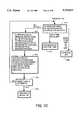
- FIG. 7which is comprised of FIGS. 7A, 7B, and 7C, there is shown a flow chart for the general alignment process which is used in training all RUs to set their delay vectors properly so as to be in alignment within the same frame.
- the processstarts as symbolized at block 180 with the CU waiting for a predetermined interval from the start of each frame and then sending a trigger signal transmission to the RUs.
- the trigger signal in each frameis a unique barker code.
- Block 182symbolizes the process wherein each RU trying to synchronize (the terms “synchronize”, “ranging” and “alignment” all are used synonymously to mean the process of training an RU to set its delay vector properly to get its alignment transmission in the gap) receives the barker code trigger signal transmission from the CU and sets its receive frame timing and then sets a first delay for its delay vector. Thereafter, the RU transmits the same barker code it received from the CU towards the CU as an alignment transmission.
- the CUmonitors the gap for activity by performing a correlation mathematical function between any received signal during the gap and the barker code that was transmitted as the trigger signal. If a barker code identical to the trigger signal is received during the gap, the correlation calculation will result in a correlation peak being found in the gap. If the correlation calculation results in a peak being found, processing proceeds to the process symbolized by block 190. There, the CU broadcasts a message to all RUs indicating that it found activity in the gap. Then the process of block 192 is performed where each RU trying to synchronize sends its signature.
- each RU trying to synchronizesends its unique signature towards the CU in order to determine if that RU's barker code is the barker code the CU found in the gap and whether it is the only RU in the gap. This process is called authentication.
- Each RUhas a unique signature which comprises the transmission and nontransmission of barker codes during the gaps of a multiple frame authentication period. Specifically, the unique signature of each RU will involve transmitting the barker code during some gaps of the authentication period but not during others. The number of gaps during which the barker code is transmitted compared to the number of gaps during which the barker code is not transmitted during the authentication period is such that if only one RU is aligned to the gap and is transmitting its authentication signature, activity will be found in the gaps of the authentication interval only 50% of the time. This scheme for authentication is chosen so that the CU can detect contentions, i.e., more than one RU in the same gap, in the manner described below.
- the process of block 194 on FIG. 7Bis performed. This process involves the CU monitoring each of the gaps during the plurality of signature sequence frames in the authentication interval and performing correlations between the signals received in each of the gaps and the barker code that the CU transmitted.
- the process of block 196is performed.
- the CUcounts the number of gaps in the authentication interval that have had activity detected therein, and then compares that number to the total number frames in the authentication interval to determine if the 50% activity level limit has been exceeded.
- the process of block 186is performed.
- the CUbroadcasts a message to all RUs telling them to adjust their delays and to try again to hit the gap with their barker code transmissions.
- the process of block 188is performed wherein each RU trying to synchronize increments its delay vector and retransmits the same barker code as was received from the CU.
- the process of block 184is performed again wherein the CU monitors the gap for activity.
- the loop comprising blocks 184, 186 and 188, taken together,comprise the trial and error process which causes all RUs trying to align themselves to continually increment their delay vectors until at least one of them hits the gap.
- Block 198if 50% activity level is detected during the authentication interval, it means that only one RU is in the gap. In such a case, the process of block 198 is performed. In this process, the CU identifies the RU whose barker code transmissions are found in the gap from the unique signature sequence transmitted during the authentication interval. In other words, the CU examines exactly which gaps had correlation peaks therein and the sequence of these gaps and looks up this sequence in a lookup table listing the unique signature sequence for each RU in order to identify the particular RU that has successfully aligned itself. Block 198 is reached only if activity is detected in exactly 50% of the gaps.
- the CUAfter the CU identifies the RU, it broadcasts the identity so determined to all RUs as the last step of block 198.
- the process of block 200is performed.
- the RU with the identity broadcast by the CUrecognizes its identity in the broadcast message and enters a fine tuning mode.
- the fine tuning modeis represented by the process of block 202.
- the CUinstructs the RU which has aligned itself in the gap on how to adjust its delay vector in order to center the correlation peak calculated by the CU to the exact middle of the gap.
- the gapis comprised of 16 chips which comprise 8 chips in the middle of the gap and then 4 chips on either side of this middle group of 8. It is desirable during the fine tuning mode to get the correlation peak centered in the middle of the middle 8 chips.
- a chipis a small interval of time equal to the frame period of 125 microseconds divided by the 448 chips which comprise each frame. In other words, each chip is 279 nanoseconds in duration.
- the fine tuning process of block 202involves sending messages back and forth between the CU and the RU which has been identified as having aligned itself in the gap. These messages are sent over the management and control channels. Usually the exchange involves only one instruction from the CU to the RU saying, for example, "Increase your delay vector by 2 chips" or, "Decrease your delay vector by 3 chips". The RU then makes the instructed adjustment and retransmits the barker code. The CU again calculates a correlation peak and examines where the peak occurs in the gap. If the peak occurs in a suitable position, the CU sends a message to the RU telling it to stop adjusting its delay vector as satisfactory alignment has been achieved.
- the CUhas to reduce the number of RUs that are in the gap to one, and it starts this process by performing the process of block 204. In this process, the CU broadcasts a message to all RUs instructing only the RUs attempting to synchronize to execute their collision resolution protocols.
- each RU attempting to synchronizeexecutes a random decision whether to continue attempting to synchronize or to stop attempting to synchronize.
- Each RUwill make this decision with a 50% probability of either outcome.
- each RU that has decided to continue to aligntransmits its unique signature sequence (sometimes hereafter called a "dotted sequence") over another authentication interval using the same delay vectors that are currently set.
- the process of block 212will be performed wherein the CU broadcasts a message instructing all RUs to go back to the previous stage and to reexecute their decisions to continue or discontinue the ranging process.
- the RUsthen re-execute their decisions whether to continue or stop attempting to align themselves and retransmit their signatures during the authentication interval with the same delay timing used on the previous iteration, as symbolized by block 214.
- the process of block 216is performed to determine if more than 10 attempts to get one RU in the gap have occurred. If so, the process of block 218 is performed to return to block 180 and restart the ranging process from the top. If fewer than 10 attempts have been made, processing returns to the process of block 210 wherein the CU again monitors the gaps of the authentication interval for activity.
- the process of block 222is performed.
- the process of block 222authenticates the RU by broadcasting the identity of the RU found in the gap and then the RU is fine tuned in the manner previously described with reference to block 202.
- processingreturns to block 204 where the CU broadcasts a message to all RUs instructing them to execute their collision resolutions protocols. This process is symbolized by block 220.
- the process of adjusting the delay vector used by the CU in transmitting its trigger signal barker codecan result in loss of synchronization by all RUs in the system unless something is done to prevent this before the CU changes its delay. That is, when the CU shortens its delay vector, the RUs closer to the CU than the furthest RU will all go out of alignment unless certain measures are taken to forewarn them of the coming change.
- the first of these processesis shown in the flow chart of FIG. 8. This process will be called the dead reckoning resychronization process for lack of a better term.
- the CUconcludes, in block 240, that its delay vector needs to be altered in order to keep the farthest RUs in alignment.
- This conclusioncan be drawn in any one of a number of different ways such as by monitoring the farthest RU for continued alignment after the farthest RU tells the CU that it is aligned with the shortest possible delay vector in use. Or, alternatively, the CU can send out a message to the farthest RU periodically inquiring as to whether it is still aligned.
- This messagecan take the form of a request for that RU to transmit its authentication signature and then monitoring the next few frames of an authentication interval to determine if that farthest RUs authentication signature shows up in the authentication interval gaps. If the CU concludes in block 240 that it needs to alter its delay vector it then alters the delay vector.
- the RUshave a predictable periodic signal from the CU upon which they can rely to measure the timing change made by the CU.
- the time of arrival of the barker code from the CU during each frameis predictable to each RU, and when it changes, the RUs can measure by how much it changed.
- the RUsknow that the CU has just altered its delay vector.
- the RUsthen measure the deviation of the new receive frame timing reference, i.e., the time of arrival of the barker code trigger signal from the CU, by measuring the difference between the old receive frame timing reference and the new receive frame timing reference. This process is symbolized by block 242.
- each RUrealigns itself in the process of block 244.
- each RUalters its delay vector by an amount equal to the change in the receive frame timing reference.
- each RUinitiates a ranging process.
- the CUmonitors the gap at the end of every frame so any RU can initiate ranging at any time.
- FIG. 9represents the preferred process for resychronizing all RUs after the CU has changed its delay vector. This process will be called the precursor embodiment herein.
- This processstarts with block 246 wherein the CU concludes that it must alter its delay vector to allow the farthest RUs to synchronize to the same frame as the nearest RUs.
- the CUafter reaching the conclusion that a change in its delay vector must be made, broadcasts a message to all RUs indicating when and by how much it will alter its delay vector.
- each RUreceives the broadcast and alters its delay vector by an amount equal to the amount that the CU will be changing its delay vector at the specified time. That is, each RU alters its delay vector by the amount instructed by the CU at the time indicated in the message from the CU that the CU will alter its delay vector.
- the final embodiment for resychronizing after the CU changes its delay vectoris for the CU simply to broadcast the message to all RUs saying, "You must all now realign as I have just changed my delay vector.” Each RU then reenters the alignment process symbolized by FIGS. 7A, 7B, and 7C. This process is repeated by each RU until all RUs are aligned.
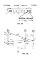
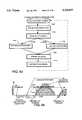
- FIG. 10there is shown a typical cable television system arrangement in which the teachings of the invention find utility in a multi-RU, multichannel environment.
- the central unit or CU 252is coupled via a coaxial cable, satellite link, microwave link, fiber optic link or some combination of these media 251 to a plurality of subscribers of which subscribers 254 and 256 are typical.
- the CUsends and receives digital information bidirectionally with each subscriber's RU.
- Each subscriberhas a remote unit or RU which acts as the interface between the subscriber's television, computer, telephone and other devices and the transmission media 251.
- the CUhas a modem therein including circuitry in a transmit channel that assembles frames of data symbols from a TDMA digital data input stream, and encodes and transmits these frames of symbols to the RUs using orthogonal codes.
- the modemalso includes a receive channel which receives the encoded frames of symbols, decodes the symbols using the transpose of the code matrix of the orthogonal codes used by the RU's to transmit the frames, reassembles the TDMA digital data stream from the decoded results and outputs the TDMA stream for use by other equipment providing various services to the subscribers.
- Each frameis comprised of symbols that are composed from digital payload data in 128 timeslots in the TDMA stream.
- Each time slot in the TDMA streamcan carry 8 bits in some embodiments, but in the preferred embodiment, each timeslot carries 9 bits for reasons to be described below.
- Each timeslotis a channel which can carry digital data encoding some service such as video on demand, video teleconferencing, internet access, etc.
- the timeslots/channelsare assigned on an as-needed basis to the various subscriber RUs to transmit/receive data implementing the service in bidirectional communication with the CU.
- a frame of dataalso comprises 128 timeslots, each carrying 8 bits of data.
- Each RUis in synchronization with the CU and knows when the beginning and end of each frame of data occurs.
- Each RUalso knows which timeslot(s) has/have been assigned to it by virtue of side conversations each RU has with the channel assignment circuitry in the CU on the command and control channels (the remaining 16 channels of the 144 total channels).
- FIG. 11there is shown a block diagram of the system of FIG. 10 which shows more detail about one multichannel embodiment for the internal structure of each RU modems transmit channel circuitry for transmitting data to the CU.
- Dashed box 254represents RU#1 while dashed box 256 represents RU#2.
- Each RUreceives a time division multiplexed (TDMA) stream of digital data from the various devices that share the communication capability of coaxial cable/transmission media 251.
- RU#1is coupled to an interactive television 258, and is also connected to a personal computer 260 and a videophone 262.
- An interactive televisionis a modified conventional TV wherein a user can send digital signals to the CU in response to things he or she sees on the television or as requests for specific video selections.
- Each of these deviceshas a digital data input/output port which is coupled to a time division multiplexer switch 264.
- the switch 264combines data coming in from devices by placing bytes of data from each device into timeslots in a time division multiplexed (TDMA) stream of digital data on line 266.
- TDMAtime division multiplexed
- the TDMA stream for RU#2is on line 267.
- Each timeslot/channelcan contain 9 bits of which 8 bits are devoted to encoding the data for that channel and 1 bit is used for management and control purposes.
- the 9th bitcan be used as a tiny side channel for side conversations over and above the main data traffic for the channel. In alternative embodiments, any other number of bits per timeslot may also be used.
- the 9 bit groups of bits in each timeslotare divided into three 3-bit groups called triple bits or tribits herein. These three triple bits from the time domain are a very short burst of data which get spread out in time in the code domain.
- the triple bitsare spread out over time by selecting three different triple bit columns from an array in a framer memory described below for each incrementation of the read pointer and multiplexing these linear arrays of triple bits through the transmitter circuitry.
- the three columns of triple bits of each frameeach span all 144 time slots of the TDMA input streams.
- All symbols generated for the first frame for all active channelsare encoded using orthogonal codes, and the results are combined for simultaneous transmission over the shared transmission media using a synchronous CDMA modulation scheme.
- Each RUis capable of receiving data in up to 144 of the timeslots in the input TDMA stream and is capable of getting all that data to the CU. However, only 144 total channels are available for all RUs to share, so rarely does one RU use all 144 channels.
- Each RUrequests the number of timeslots or channels it needs to provide services requested by the subscriber. This request is sent via a message on a command and control channels to the CU. The CU then sends a reply message telling the requesting RU which channels have been assigned to it. The CU will not assign the same channel to multiple RU's.
- Each RUthen uses the appropriate orthogonal codes in the encoders coupled to receive the data from the timeslots to which it has been assigned. For example, if RU#1 is assigned channels 1 and 2, and RU#2 is assigned to channel 3, RU#1 will use orthogonal codes #1 and #2 in the encoder coupled to receive the data in timeslots 1 and 2, and RU#2 will set orthogonal code #3 into the encoder coupled to receive the data from timeslot 3. That is, one orthogonal code is assigned to each payload channel and each command and control channel in the embodiment shown in FIG. 11.
- the transmit channel of each RU of the embodiment shown in FIG. 11has a splitter like splitter 268.
- the purpose of this splitter in transmitting data to the CU 252is to split out the data in each time slot of the time division multiplexed incoming data stream and apply the data from each time slot to one of a plurality of orthogonal code encoders for encoding using one orthogonal code from the code set used on the system.
- the data from time slot #1is output from the splitter on line 270 which is coupled to the data input port of orthogonal code #1 encoder 1, block 272, and the data from time slot 2 is sent via line 271 to encoder #2, block 273.
- the encoder 272encodes the channel 1 data from time slot 1 using code #1 of the orthogonal code set in use in the system (actually, one row of the code matrix that defines the entire code set), and outputs the resulting modulated signal on line 274 which is coupled to one summing input of a summer node 276.
- Encoder #2, block 273,encodes the data from channel 2 in time slot 2 using code #2 from the orthogonal code set (a different row of the code matrix--rows or columns of the code matrix may be used interchangeably in the matrix multiplication of the transmit process so long as the matrix multiplication of the received signal vector times the transpose matrix is the opposite, i.e., if rows are used on the transmit side, columns are used on the receive side).
- a controller circuit (not shown) in each RUwhich is coupled to communicate with the CU over a management and control channel and which is also coupled to each of the orthogonal code encoders, receives the channel assignments for the RU and selects the unique orthogonal code for the channel assigned. The controller circuit then controls each encoder to use the appropriate orthogonal code assigned to the channel when encoding data for that channel.
- Each encoder in the RUs which is activemust use a different, unique, orthogonal code. No encoder will use the same code as another "active" encoder.
- An "active" encoderis an encoder which has been assigned to encode a particular channel for its RU.
- the data in the assigned timeslots/channels for each RUis encoded. This is done using the appropriate orthogonal codes assigned to those channels.
- the resultsare then transmitted to the CU simultaneously from all RUs over the shared transmission media 251. More precisely, the energy representing the data from the various timeslots/channels is spread out over the entire 125 microsecond duration of the frame by the action of the encoders. Because the data from the various timeslots is encoded using orthogonal codes, no interference between the data occurs during transmission of the encoded symbols in the code domain.
- Each encoderspreads out the energy from its assigned channel over all the chips in the frame.
- Each encoder in each RUhas its encoded output signal coupled to a summing input of a summer like summer 276.
- the function of the summer in each RUis to sum all the encoded signals and output them on a subscriber branch coaxial cable or other transmission media like branch cable 278.
- the transmission media like branch 278are coupled through a directional coupler like coupler 280 to the main coaxial cable/transmission media 251.
- the combined output signals from each RUare added to the composite signal on the main coaxial cable by one or more directional couplers symbolized by coupler 280.
- the code domain signals on shared transmission media 251are decoded by the decoders 282, 284 etc., and the resulting data is put back into the appropriate timeslots in the time domain TDMA data streams for output to the various equipment that is providing the requested services.
- the composite signal received from transmission media 251is distributed to each of a plurality of decoders.
- a decoder for channel 1is represented by block 282. This decoder uses the transpose of the code matrix which was used to encode the channel 1 data to extract any channel 1 information encoded into the composite signal by RU#1 (or whatever RU was assigned to channel 1). This decoding is done in the manner described previously in the discussion of FIGS. 1-3.
- the decoder for channel 2represented by block 284, using the transpose code matrix to decodes any channel 2 information encoded into the composite signal by RU#2.
- each decoderuses the appropriate column of the transpose matrix c T ! corresponding to the code used by the corresponding RU to encode the channel being decoded.
- the resulting decoded digital signalsare output on lines 286 and 288 to a switch which reassembles these digital signals to reproduce a composite of the time division multiplexed data streams which entered the RUs on lines 266, 267 etc.
- each transmit channelIn the embodiment shown in FIG. 11, only the transmit channels are shown and individual encoders are shown for each channel. In a more practical embodiment, only a single encoder is used in each transmit channel in each modem. This encoder is time shared to encode the data from the various timeslots. Usually, the single encoder is a suitably programmed microprocessor. Each RU modem also has a receive channel (not shown) which is structured similarly to the receive channel circuitry in the CU shown in FIG. 11. In some embodiments, the decoding in the receive channel and the encoding in the transmit channels are both done using a single microprocessor which has been suitably programmed. The choice of whether to use a shared microprocessor or multiple individual channels of hardware is largely dependent on data rate and cost considerations. If the data rates are high, multiple individual channels may be required. If data rates are low enough to use a shared microprocessor and cost is to be minimized, the shared microprocessor is preferred.
- the orthogonal code set selectedmust have at least 128 codes.
- an orthogonal code set having at least 144 unique, orthogonal codesmust be used. Each channel has a maximum 72 kilobits per second data capacity in the preferred embodiment.
- Channel allocation by the CUcan take any one of a number of different forms.
- the RUscould have a fixed allocation of channels or channels could be awarded in any number to any RU based upon need where the CU polls the individual RUs for their needs or the RUs transmit their needs asynchronously to the CU and the CU arbitrates between the requests to allocate the available channels.
- one RUmay have security considerations the require one channel to be dedicated to it at all times and no other RU is allowed to be on that channel as controlled by channel awards by the CU given in messages to the individual RU's.
- some channelscan be made available for all RUs to use with the RUs themselves resolving contentions.
- all four schemescan be used individually at times or any combination of the schemes can be used at times. Which channel allocation schemes are in use at particular times is established by the configuration data set up by the user. For example, one fourth of the channels may be put on a reservation scheme, one fourth of the channels may be left for contention, one fourth of the channels may have fixed allocation and the last fourth of the channels may be reserved for polling allocation.
- Each of these different mechanisms for allocation of bandwidthis believed to be known, standing alone. However, the applicant's believe it is new to provide a CU that can use any one of these methods or any user programmable combination of all four methods for user programmable groups of channels, all as established by entry of configuration data by a user during a configuration process.
- the RUsSince the channel allocation mechanism is centralized in the embodiment of FIG. 11, the RUs have no burden other than to ask for the bandwidth they need. However, in alternative embodiments, the RUs may "bid" for channel allocations and some arbitration process carried out locally in the RUs may resolve any contentions.
- each RUwould have a fixed assignment of time slots, and those time slots would be transmitted even if they were empty, i.e., the RU had no traffic to send or receive during some or all of its time slots.
- Synchronous TDMA multiplexing schemesare described in "Data and Computer Communications" by Dr. William Stallings, at page 211-213, Macmillan Publishing Co., New York (4th Ed. 1994) ISBN0-02-415441-5 which is incorporated by reference herein.
- FIG. 19there is shown a block diagram of the preferred embodiment of a transceiver for use in the modem of each RU and CU.
- the transmit channel of the transceiveruses a framer 400 to compose from the TDMA data stream the symbols of each frame for encoding and transmission.
- the output data stream from the frameris an array of tribits that span the entire 144 timeslots, with three such arrays presented during each frame. Each tribit is a symbol in a frame for transmission.
- the circuitry of the transceiveris virtually all digital, so the arrays of tribits are true arrays elements of which are used sequentially in the matrix multiplication of orthogonal encoding.
- the arrays of tribitswill be streams of tribits, with three separate streams per frame.
- the RU's and CUall utilize framer circuitry to implement the delays needed to transmit data in synchronization to each other.
- the frameris comprised of a FIFO memory and supporting circuitry that stores incoming digital data from the time division multiplexed data stream received by each RU and CU.
- the symbols of each frameare composed by output of the data from the FIFO memory in a different way than it was loaded during each frame.
- the basic ideais to pass the 9 bit groups of each time slot through the analog of a FIFO delay line implemented by a memory so as to simultaneously implement the delay imposed by each RU and CU needed for synchronization while providing a convenient way to compose the symbols of each frame from the data in the TDMA data stream.
- FIG. 12shows the circuitry that implements the framer in the preferred embodiment
- FIG. 13shows the timing relationships between the chip clock signal which sets timing in the code domain and the bit and byte clocks which set timing in the time domain.
- FIG. 13also shows a number of other signals generated by time base generator 350.
- the basic period from which all other signals are generatedis the chip clock signal shown on time line T1 of FIG. 13.
- the relationships between the periods of the various signals in FIG. 13is shown in parentheses at the right edge of each signal. For example, for the bit clock signal shown on time line T2 of FIG. 13, for every 7 periods of the chip clock signal, there are 16 periods of the bit clock signal. For every 7 periods in the chip clock signal, there are two periods in the byte clock signal shown on time line T3 in FIG. 13. Handling of the TDMA stream is synchronized to the bit clock and byte clock signals.
- the chip clock signal on line 348 of FIG. 12is generated by a time base generator PLL 350 and is synchronized with the TDMA data stream by the action of the PLL in keeping both the chip clock and bit clock signals synchronized with the crystal oscillator reference signal.
- a block diagram of the time base generator 350is shown in FIG. 18.
- a voltage controlled oscillator 353 operating at a frequency of 114.688 Mhzsets the basic operating frequency.
- the output frequency of the VCO on line 357is divided by two by a divide-by-two counter 359. The result is coupled to one input of a multiplexer 361.
- the multiplexerhas as its other input the crystal controlled oscillator frequency on line 363.
- the multiplexer switchingis controlled by a bypass signal on line 365 so as to normally select the output of the counter 359 and couple it to output line 367.
- the PLL time base generatorgenerates the bit clock signal on line 377 by dividing the frequency of the signal on line 367 by a factor of 7 in a divide-by-seven counter 369 to generate a bit clock signal on line 377 having a frequency of 8.192 Mhz.
- the chip clock signal on line 348is generated by dividing the frequency on line 367 by a factor of 16 in a divide-by-16 counter 371 to generate a chip clock signal having a frequency of 3.548 Mhz.
- the bit clock and chip clock signalsare kept synchronized to the crystal frequency by a phase detector 373 which compares the phase of the crystal signal to the phase of the bit clock signal and outputs a signal which is coupled to the frequency control input 375 of the VCO through a low pass filter 379.
- the bit clock signal and phase detectorcauses the PLL to force the transitions of the chip clock signal to line up properly with the bit clock transitions in the relationship of 16 periods of bit clock for every 7 periods of chip clock.
- timing in the time domainis as follows:
- Each time slot or channel in the TDMA streamscarries 9 bits of digital data synchronized with the bit clock;
- One time slot worth of data or 9 bitsis stored in the framer for each cycle of the byte clock;
- the byte clock signal on line 302is generated by a byte counter 370 shown at the top of FIG. 12 which generates a byte clock signal transition on line 302 every 9 cycles of the bit clock signal on line 377 from the time base generator 350.
- Data from the time slots/channels in the time division multiplexed stream of serial data on line 301is shifted serially into a serial-in, parallel-out shift register 310 at the bit clock rate of the signal on line 377.
- the byte clock signal on line 302causes a register 314 to store the current 9-bit, parallel format output of the shift register on bus 316 after each 9 new bits are shifted into shift register 310.
- the 9 bit parallel format output of the register 314is presented on 9-bit bus 318 to the write data input port of memory 300.
- a new 9-bit group of data from the TDMA streamis presented for storage on each cycle of the byte clock signal.
- Each 9-bit group of data from the TDMA streamis stored in a different memory location of memory 300 as will become clear from the discussion of the address generation circuitry described below.
- Datais read out of memory 300 at the same rate at which it was stored, but starting at some programmable time after the data is stored, thereby implementing the variable delay needed to maintain frame synchronization with the CU frame timing.
- This programmable delay T dis set by the difference in addresses between the address stored in a receive frame counter (read pointer) and the address stored in a transmit frame counter 324 in FIG. 15 (write pointer).
- FIG. 16represents portions of memory 300 with the stippled portion representing the number of addresses difference between the position of the read pointer and the position of the write pointer to implement the delay T d .
- the cross hatched portion 304represents one frame of 9-bit bytes while the stippled portions 306 and 308 represent the amount of the delay T d , where portion 306 represents a portion of the delay T d expressed in full 9-bit bytes, and portion 308 represents the remainder of the delay T d expressed as part of a byte.
- the delay T dmay be some fraction of the number of bit clocks making up an entire 9-bit byte. This is because the delay needed to maintain frame synchronization may not work out to be an integer number of byte clocks.
- FIG. 15shows how the time delay T d is implemented using a receive frame counter 322 that generates the write pointer address controlling where incoming data is stored in the memory 300 and a transmit frame counter 324 that generates a read address pointer that controls the read address from which data is read for transmission.
- the F -- sync signal on line 326resets the write pointer in counter 322 to zero at the beginning of each new frame.
- a modulo adder 326adds the number of chip clocks based upon the desired time delay T d to the output write pointer on bus 328 and inputs the result into the transmit frame counter 324 as the read pointer.
- T dThe value of T d is varied on a trial and error basis during the synchronization process until the gap is hit and the CU sends a message to whatever RU is synchronizing telling it to freeze T d at the value that caused the gap to be hit by the barker code.
- FIG. 14is a memory filling diagram that illustrates how entire 9-bit bytes are received continuously, while 3-bit tribits for each of 144 channels are sent out simultaneously to compose the symbols of each frame.
- FIG. 14graphically illustrates how the frame memory 300 fills and is emptied during this process.
- Frame memory 300has 144 memory locations corresponding to the 144 channels of the system on each of three pages. While one page is being filled, another page is being simultaneously emptied at the same rate.
- Each memory address on each pagecan store the 9 bits of data from one of the 144 time slots in the TDMA stream.
- 16 memory locations on each pageare reserved for the storage of management and control data to be sent across the 16 management and control channels. In FIG. 14, address numbers increase with an increasing Y coordinate.
- page one of the memoryis shown as completely full with one frame of data comprised of three vertical columns of three cross-hatched blocks apiece.
- Each column of three blocks, such as blocks 334, 336 and 338represent one symbol, each symbol having 48 tribits therein.
- the middle column of FIG. 14represents the state of fill of the memory after transmission of the first symbol comprised of blocks 334, 336 and 338.
- the rightmost column of FIG. 14represents the state of fill of the memory after transmission of symbol 2 comprised of blocks encircled by dashed line 334.
- the width along the X axis of each individual crosshatched block in FIG. 14is equal to the 3 bits of a tribit, and the entire width of a column of blocks is equal to the 9 bits of a time slot.
- the positive x directionrepresents increasing time in the time domain. In other words, the first 9-bit byte that is stored is stored in the lowest row of the lowest three blocks in the left column with increasing time in the TDMA stream extending from left to right.
- the blocks surrounded by dashed line 332 in the leftmost columnrepresent 144 memory locations, each storing the 9 bits from one of the 144 time slots in one frame of data.
- the three crosshatched blocks 334, 336 and 338represent the first symbol of the first frame, each symbol storing 48 tribits. Note in the middle column, after transmission of the first symbol in the frame, these three blocks are gone. Note also that the data of symbol 1 is read out of the memory "across time", i.e., along the y axis, thereby interleaving the data from the first tribits of individual channels in the time domain into different temporal relationships in the code domain and spreading out the energy of the time slot data over the entire frame interval. This is part of the teaching of code division, multiple access or CDMA modulation schemes.
- the three blocks within dashed box 334 in the middle column of FIG. 14represent the second symbol of data that is to be transmitted in the first frame. Note that these three blocks are gone in the rightmost column representing the state of page one of the memory fill after transmission of the second symbol.
- the blocks encircled by dashed box 340represents the delay T d implemented by modulo adder 326 in FIG. 15 and the 16 chip alignment gap.
- FIG. 17is a diagram of the relative rates of address incrementation of the read and write pointers used to manage the framer buffer memory 300 including the relative timing of address incrementation for reading the tribits.
- Dashed line 342represents the rate of address incrementation of the write pointer generated by counter 322 in FIGS. 12 and 15. This counter counts transitions in the byte clock signal on line 302 in FIG. 12, with the byte clock signal shown on time line T3 in FIG. 13. Every cycle of the byte clock signal causes register 314 in FIG. 12 to latch a new 9-bit byte therein and present it on bus 318 to the write data port of two-port memory 300.
- Every cycle of the byte counteralso causes write pointer counter 322 to present a new write pointer address on bus 366 for use in controlling where the data on bus 318 is stored.
- a multiplexer 362having its output coupled to the address port of memory 300 and having as its inputs the write pointer on bus 366 and the read pointer on bus 364 is suitably switched so that the write pointer and read pointer addresses are presented at the appropriate times at the address port to implement the memory filling and memory reading operations described herein.
- the bit clock signal on line 377 in FIG. 12is used to clock the serial-in, parallel out shift register 310.
- the bit clock signalis generated by the time base generator shown in FIG. 18 and is counted by a modulo 9 bit counter 372 shown at the top of FIG. 12 for purposes of helping generate the byte clock signal on line 302 in FIG. 12.
- This counter 372counts the bit clock signal on line 377 from time base generator 350 modulo 9 and outputs a transition to logic 0 on line 374 after every 9th bit period.
- the transition on line 374acts as a count enable signal to byte counter 370 to enable incrementation of the byte counter 370 by the next bit clock cycle. This generates the byte counter signal on line 302.
- the bit counter 372is always enabled by the hard wired count enable signal on line 376. Both the bit counter and the byte counter are reset to 0 by asserting the F 0 signal on line 373 for fast resetting/resynchronization of the system.
- the F 0 signaloccurs at the end of each frame.
- the F 0 signalis generated by a portion of the time base generator not shown in FIG. 18, and is counted as a clock signal by frame counter 375 which outputs a synchronized F 0 signal on line 373.
- the frame counter 376is reset every 4th frame by a super frame signal F 4 .
- the time delay T d necessary for hitting the alignment gap with a barker code transmissionis added to the F 0 signal on line 373 by the modulo adder 326 to generate the F 0 ' signal on line 381.
- the F 0 signal on line 373also increments the page pointer 321 for the write pointer and simultaneously resets the write pointer 322 to zero at the end of each frame so as to begin writing again at address 0 of the next page.
- the delayed F 0 ' signal on line 381increments the page pointer 323 of the read address circuitry and simultaneously resets the read pointer counter 324 to zero so as to begin reading at address 0 of the next page at the end of the frame.
- solid line 346represents the rate of emptying the frame memory 300 in FIG. 12. This rate of emptying is based upon incrementation of the read pointer counter which counts the chip clock signal on line 348 from time base generator 350. Since each symbol stores 144 tribits from 144 different channels and since there are three symbols and a 16 chip gap in each frame, the total number of chips in a frame is 448. Since all the 432 tribits of all three symbols of the frame must be read out while the byte counter is counting to 144 to store a frame's worth of 9-bit bytes of data from 144 channels or time slots, the read pointer is incremented on the chip clock signal.
- Line 352 in FIG. 17represents the rate of incrementation of the read pointer counter 324 in FIG. 12.
- the read pointer counterincrements on each cycle of the chip clock signal such that it increments from 0 to 143 during the time to read all the tribits from the first symbol. This has the effect of causing the 9 bits of data from each of the 144 timeslots or channels to appear sequentially at the read data output bus 358. However, it is desired to only unload all 144 tribits from a single symbol during one symbol time, so some switching on the output bus is needed, as described below.
- FIG. 20is a diagram which helps illustrate the manner in which framer memory 300 is emptied for transmission.
- FIG. 20shows a completely filled page 1 of memory 300 in FIG. 12 comprising 144 memory addresses, each filled with one 9-bit byte, and divided into three columns of 3-bit tribits.
- Each column, marked by the legends symbol 1, symbol 2 and symbol 3is comprised of 144 tribits and represents one symbol of a frame.
- the read pointerwill increment 144 times during the time the first symbol is being encoded.
- the state of the tribit select counter during this first 144 cyclesis such that only the 144 tribits of symbol 1 will be output on bus 360 to the ECC encoder 402.
- the read pointer counter 324rolls over to zero and begins to count up to 143 again.
- the tribit select counterincrements which causes the multiplexer 356 to select the middle column of tribits from symbol 2 in FIG. 20 for output on bus 360 in FIG. 12 to the ECC encoder 402 in FIG. 19.
- a similar processunloads the 144 tribits of symbol 3.
- Bus 360 in FIG. 12is coupled to ECC encoder 402 in FIG. 19.
- the ECC encoderis a state machine which, in conjunction with state memory 404, receives the stream of tribits and calculates a 4th ECC bit for each tribit. This 4th bit provides redundancy for error detection and correction and for use by a Viterbi decoder in the receiver in ascertaining with greater accuracy the data that was actually sent despite the presence of noise.
- the stream of 4-bit symbol elements that are output from the ECC encoder 402are stored in memory 406 as three different linear arrays corresponding to symbols 1, 2 and 3 in FIG. 20.
- a multiplexer 362 having its output coupled to the address input of the framer memory 300has two inputs: one is coupled to the output of the read pointer counter 324 and the other is coupled to the output of the write pointer counter 322.
- This multiplexeralternately couples the read pointer on bus 364 and the write pointer 366 to the address port 368 of the memory 300 on every cycle of the chip clock signal on line 348.
- the chip clock signalis also coupled to the control input of the memory 300 to serve as the RD/WR* control signal controlling whether the memory uses the address at port 368 in a read or a write transaction.
- the output data streams from the framer on bus 360may optionally be passed through an ECC encoder to add redundancy by calculating a 4th ECC bit for each tribit.
- the ECC encoderis used to provide greater accuracy and better noise immunity.
- the ECC encoderin the preferred embodiment, is a state machine but it could also be a lookup table. For purposes of this discussion, it will be assumed that the ECC encoder is present.
- the output of the ECC encoderis an array of 4-bit digital numbers for each of symbols 1, 2 and 3. Each of these 4-bit numbers has two bits representing a real part and two bits representing an imaginary part. This convention is used to facilitate the constellation of input point mappings shown in FIG. 21.
- FIG. 21maps each of 16 possible input points, i.e., permutations of the 4 bits in each symbol array to a point in space defined by the in-phase or I axis for the real part and the quadrature or Q axis for the imaginary part of each point.
- FIG. 22is a table listing all the possible 16 combinations of 4 bits in the Code column and the corresponding 2's complement digital representation of the real and imaginary coordinates for each combination in the Inphase and Quadrature columns, respectively.
- the input point 1100maps to a point having a +3 imaginary coordinate and a -1 real coordinate on the constellation of FIG. 21.
- the mapping of FIG. 21was selected to give maximum separation between points in the constellation for best noise immunity, but any other mapping would also work.
- 2's complement representationis not required for the coordinates as they can be represented in other number systems as well.
- each symbolis comprised of two linear arrays of 2 bit numbers: one array contains multiple 2-bit elements defining the real or inphase coordinates for all the elements of the symbol and the other array stores the 2-bit elements which define the imaginary or quadrature coordinate of each symbol element.
- the 144 array elements of each symboldefine an information vector b for each symbol.
- FIG. 23shows the matrix multiplication process which is performed within code division multiplexer 408 in FIG. 19 to multiply each of the two linear arrays that define each symbol times the orthogonal code matrix c!.
- the matrix multiplicationis performed by a microprocessor, but any machine that can do the matrix multiplication will suffice to practice the invention.
- the encoding in CDMA Mux 408 using the orthogonal or orthogonal, cyclic codesis done in two steps.
- a linear array information vector of just real or inphase coordinates of the symbol to be transmittedsymbolized by array 405 in FIG. 23, is multiplied by the code matrix 407.
- This operationgenerates another linear array of real or inphase coordinates along the R axis of a result space in a results constellation similar to the constellation of all possible input points shown in FIG. 21.
- This first linear array 409defines the real axis coordinates in the result constellation for a plurality of chips from the first symbol to be transmitted.
- the real component arrayrepresented by linear array 409, is part of an overall result or "chips out" array which contains both the real and imaginary coordinates of a plurality of chips to be transmitted. These chips map to points in the result space, and the points in the result space map to whatever points in the input point space that are defined by the real and imaginary components in the information vector array b, of which array 405 is the real part.
- the mapping between the input point space and the results spaceis defined by the contents of the code matrix and the orthogonal codes.
- FIG. 23is a simplified version of the system in which there are only 4 channels resulting in 4 elements of each symbol.
- the 4 real components of the information vector b shown in array 405 after conversion to their decimal equivalents,are, respectively, +3, -1, -1 and +3.
- This column of numbersis multiplied by the first row in the code matrix to yield the result 4 as the first real component in array 409 of the results array.
- arrays 405 and 409would be 144 elements long, and the code matrix 407 would have 144 elements in each row and would have 144 rows.
- the resulting real and imaginary component linear arrays of the results or chips out arrayare stored in a memory within the CDMA Mux 408 which is not separately shown.
- the components of these two arraysare then output on separate I and Q buses to a modulator 410 where they are used to amplitude modulate the amplitudes of two RF carriers that are 90 degrees out of phase.
- the resulting two AM carriersare summed and output on the shared transmission media 412. This is done as illustrated in FIG. 24.
- the result or chips out array 411is stored in memory 411 within the CDMA Mux 408, and comprises the real or inphase array 409 and the imaginary or quadrature array 413 of the 144 result points or chips in the result space.
- one result point or chipcomprising a real component and an imaginary component is output on bus 451 to a bit parsing unit or bit splitter 453.
- the bit parsing unit 453splits off the real component and outputs those bits on bus 417.
- the imaginary componentwill be parsed out, and those bits will be output on bus 419.
- two optional digital passband filters 421 and 423are used to limit the bandwidth of the signals on buses 417 and 419 to 6 Mhz to avoid interference with signals on neighboring frequencies.
- the digital signals on buses 417 and 419, when converted to their decimal equivalentsusually have rapid transitions between levels in adjacent intervals. This is illustrated in FIG. 25 which is a plot of the changes in amplitude over time of the real components of the results vector for the array 409.
- These filters 421 and 423are low pass filters which remove high frequency Fourier components caused by sharp edges in such signals which effectively round off corners of such signals and limit most of the power density in the Fourier spectrum of such signals to a 6 Mhz band centered around the frequency of the RF carrier generated by local oscillator 425.
- This local oscillatorgenerates a sine wave, RF carrier at a frequency selected to be compatible with the switching rate of multiplexer 408 and to not interfere with existing cable TV service signals on adjacent frequencies.
- the local oscillator cosine waveis applied to the carrier input 427 of an amplitude modulator 429 which also receives the filtered real component of each chip on bus 431.
- the modulator 429modifies the amplitude of the carrier signal on line 427 in accordance with the amplitude of the decimal equivalent the real component on bus 431 and outputs the result on bus 443.
- the imaginary or quadrature component of each chip, after filtering,is input on bus 433 to another amplitude modulator 435.
- This modulatorreceives at a carrier input 437 a sine wave of the same frequency as the cosine wave on line 427, but shifted in phase by 90 degrees by phase shifter 439.
- Modulator 435modifies the amplitude of the sine wave in accordance with the amplitude of the imaginary component on bus 433, and outputs the result on line 441.
- Lines 441 and 443are coupled to a summer 445 which sums the two waveforms and outputs them on the shared transmission media via line 412.
- the line 412may be coupled to suitable interface circuitry to drive the signal on line 412 into a wireless or cellular system, a terrestrial microwave link, a coaxial cable of a cable TV, telephone or other system, a fiber optic link of a cable TV, telephone or other system, a local area or wide area network or any other media developed in the future for real time communication of data.
- suitable interface circuitryis known and will not be described further herein.
- the receiver side circuitry of the transceiverwill be described in more detail.
- the processing performed in the receivermay be performed using analog or digital or some combination of analog and digital circuitry.
- the receiverwill be described as if all processing was digital as it is in the preferred embodiment.
- the signal received from the shared transmission mediais passed through an analog-to-digital converter (not shown) and the resulting digital data stream is passed to a demodulator 460.
- FIG. 26is a more detailed diagram of the structure of the demodulator.
- the received analog signal from the shared transmission mediais coupled on line 461 to the analog input of an A/D converter 463.
- the stream of digital datais simultaneously fed to two multipliers 465 and 467.
- Multiplier 465receives as its other input, a stream of digital values that define a sine wave having the same frequency as the RF carrier sine wave on line 437 in FIG. 24.
- Multiplier 467receives as its other input, a stream of digital values that define a cosine wave having the same frequency as the RF carrier cosine wave on line 427 in FIG. 24.
- the results output on lines 469 and 471is a digital data stream which basically defines the mix products comprised of a fundamental carrier frequency and upper and lower sidebands.
- Digital filters 473 and 475filter out the desired sidebands that contain the real and imaginary parts of each chip or result point that was transmitted.
- the stream of quadrature or imaginary components of the received chipsare output on bus 477.
- the stream of inphase or real components of the received chipsare output on bus 479.
- the streams of real and imaginary components of the 144 chips of each symbol on buses 477 and 479are stored in two linear arrays in CDMA Demultiplexer 462 in FIG. 19.
- the CDMA Demultiplexer 462multiplies each of the real and imaginary component arrays times the transpose of the code matrix used by the CDMA Mux 408 of whatever RU or CU that transmit the data to reverse the orthogonal code encoding process. This matrix multiplication process results in two linear arrays of decoded chip real and imaginary parts for each symbol. These arrays are stored by the CDMA demultiplexer 462 in memory 464.
- the CDMA Demultiplexerprocesses the two streams if real and imaginary components "on the fly" such that they do not have to be first stored as input arrays in a memory in the CDMA Demultiplexer 462.
- the result for each symbolis an array of received chip points in a received chip space having a real axis and an imaginary axis.
- the mapping by orthogonal code transformation from the constellation of possible input points shown in FIG. 21leads to a constellation of possible points in a received chip space.
- a detector 466examines the points in each of the arrays and compares the received chip points they define against the legitimate possible points in the received chip space.
- the detectorotherwise known as a slicer, is a known type of circuit and no further details are necessary herein.
- the function of the detectoris to compare each received chip point and compare each point against the closest points in the constellation of legitimate possible points in the received chip space that could have been transmitted. The detector then makes a preliminary decision as to which the possible legitimate points in the received chip constellation each received chip is likely to be.
- the detector 466then outputs its preliminary determinations to a Viterbi decoder 468.
- Viterbi decodersare well known in the art of digital communications, and no further details will be given here except to state its function.
- the Viterbi decoderuses the 4th ECC bit in each 4 bit component of each symbol to detect and correct errors. This is done by performing the Viterbi algorithm to derive the most probable tribit path defined by the points actually sent from the path in the received chip space defined by the 4-bit components of the symbols actually received, after they have been processed by the detector. This Viterbi algorithm could be carried out by a programmed digital computer or by a dedicated hardware circuit.
- the output data points from the Viterbi decoderare a stream of tribits. These tribits are stored in a memory in a deframer circuit 470 which functions to reassemble a replica of the TDMA data stream in the time domain from the incoming stream of chips or tribits comprising each symbol. This process is done by reversing the reading and writing processes described above in filling and emptying the framer memory 300 of FIG. 14. AN IMPLEMENTATION OF THE DATA LINK AND MAC LAYERS USING AN ATM PROTOCOL
- FIG. 27there is shown a block diagram of a preferred embodiment of a system for implementing ATM protocol transmissions over a shared hybrid fiber coax (hereafter HFC) cable television network.
- the circuitry to the left of the shared HFC network 1000represents the circuitry in the CU.
- the circuitry to the right of the HFC media 1000represents the Customer Premises Equipment (hereafter CPE or RU) for customer #1.
- CPECustomer Premises Equipment
- the CU systemis comprised of a SAR circuit 1002 which is coupled to a plurality of devices and other networks that supply data for transmission to the CPEs and which receive data from the CPEs.
- device #1could be a video on demand player for receiving requests for pay per view movies and, in response thereto, mounting the requested movie and output of the video and audio tracks therefrom as a stream of digital data on bus 1004.
- device #ncould be an Ethernet or ATM network interface card coupling the SAR to a local area network (not shown) using an ATM or Ethernet transport protocol.
- the SARmay also be coupled to one or more service provider or other networks.
- the block labelled network #1may be the local and long distance telephone network interface.
- the block labelled network #2may be an internet provider interface.
- All of the networks and devices to which the SAR is coupledtransmit and receive data byte streams bidirectionally on the buses like bus 1004 that connect the network or device to the SAR.
- the SARfunctions to receive the data stream from each device and network interface and packetize the data from each device or network interface into 55 byte ATM cells which are output on bus 1006 in a slightly-modified, industry-standard, time-division-multiplexed Utopia+data stream.
- Utopiais a format for a time division multiplexed data stream that has transmitted in its timeslots 53 byte industry standard ATM protocol cells.
- ATMis a network transport protocol which provides an abundance of advantages over other network protocols in delivering multimedia services.
- ATM protocolsguarantee quality of service, such as guaranteed bandwidth/bit rates, services like video teleconferencing, digital video and other high bandwidth consumption services which cannot tolerate interruptions in the flow of data can only be transmitted over ATM networks.
- the ATM protocolprovides the ability to provide integrated voice, video and data services simultaneously over a single physical media.
- SAR 1002receives these digital voice, data or video bytes and packetizes them into slightly modified ATM cells having 48 bytes of payload referred to as the cell body, 5 bytes of header information which, among other things, identifies the particular device at the RU for which the payload data is destined, and 2 bytes of "virtual link" header information.
- the virtual link header informationincludes two bytes which comprise the address of a formatter at the RU which will be explained below.
- the data from the devices or network interfaces coupled to the SAR 1002contain destination data indicating to which RU the data is bound and to which device or network interface card coupled to the destination RU/CPE modem the data is to be directed.
- This destination datais used by the SAR to compose the information in the standard ATM header and the virtual link header portions of each Utopia+cell output on bus 1006 for downstream traffic (toward the CPEs).
- This Utopia+TDMA data streamis transmitted to a multiplexer/demultiplexer 1008 which implements an interface between the ATM cells on bus 1006 and the synchronous code division multiplexed physical layer described elsewhere herein.
- SAR 1002also receives a "Utopia+" format TDMA data stream carrying upstream traffic from the CPEs and depacketizes the ATM cells in the stream and uses the header information contained in the packets to transmit each cell out on the appropriate bus to the device or network interface indicated in the header information.
- SARssegmentation and reassembly circuits
- the multiplexer/demultiplexer 1008receives the "Utopia+" time division multiplexed data stream from the SAR 1002 which contains all the downstream data originating in the devices connected to the SAR 1002 and destined for any CPE.
- the function of the multiplexer-demultiplexer 1008is to add a 9th bit to each 8-bit byte of the "Utopia+" data stream so as to encode the sequence of 9th bits in the 55 8-bit bytes of each ATM cell so as to signal the CPE where the first byte of each ATM cell starts and to add CRC or other error detection and correction code data to be used by the CPE receiver in detecting and correcting errors in the header and payload information of the 55 8-bit bytes of the ATM cell.
- the ATM-SCDMA interface 1008also serves to output the 55 converted 9-bit bytes of each ATM cell on bus 1010 as a time division multiplexed data stream having one 9-bit byte in each time slot in synchronization with the 8 MHz bit clock signal to which the circuitry in the SCDMA physical layer is synchronized. It is this time division multiplexed data stream of one 9-bit byte per timeslot on bus 1010 that is the raw data input to the synchronous code division multiplexing transceiver circuitry described above that implements the physical layer of the OSI model.
- the ATM protocolwas designed for a local area network point to point environment without a shared media.
- a "shared media”, as that term is used herein,means a media wherein more than one pair of devices may be communicating with each other either at the same time or sequentially.
- all the devicesare coupled together through individual connections such as twisted pair, coax, fiber optic waveguide etc. from the device to a switching hub or ATM switch.
- a cell of data generated by another deviceis sent via a point to point protocol in this topology by placing the destination address of the device to which the cell is addressed in the cell header and transmitting the cell to the ATM switch.
- the cellis the switched onto the appropriate branch connection from the switch to the device to which the cell is addressed or to a bridge or router which will ultimately direct the cell on an appropriate path to the device to which the cell is addressed.
- No other pair of devicescan use the various data paths involved in this transaction while the transaction is occurring as that would cause a collision and loss of data. If two devices simultaneous direct ATM cells to a single device, such as two workstations directing ATM cells to a server for storage, the two ATM cells from the different work stations arrive at the ATM switch simultaneously. In such a case, both cells cannot simultaneously be sent to the server on the single connection from the ATM switch to the server. In such a case, the ATM protocol calls for the ATM switch to buffer one cell while the other cell is being transmitted to the server. When the first cell is completely transmitted, the second cell is transmitted.
- each branching media diverging from the head end to the CPEssuch as media 1001, 1003, 1005 and 1007 is shared by the CPE peripherals of all the CPE coupled to each media.
- media 1001is shared by the peripherals connected to 4 CPE, of which CPE 1009 and 1011 are typical. None of these peripherals coupled to CPE 1009 and 1011 could simultaneously exchange ATM cells with peripherals coupled to the head end 1013 because collisions would occur on shared media 1001 causing loss of data.
- Each CPE's virtual link to the head endis not shared and is implemented by assigning specific ODMA codes to the CPE and head end transceivers.
- the shared physical medialooks logically like it is not shared since the CDMA encoding of the data prevents simultaneously transmitted data using other orthogonal codes with it.
- Each virtual linkcarries the ATM compliant cells and is the sum of all data transmitted to and received from a specific CPE.
- the focuswill be on the logical equivalent of what is happening on the physical level, i.e., the virtual traffic on the virtual links will be described instead of the actual physical signals travelling across the shared media with interleaved and scrambled bits from every byte in all 128 timeslots in every symbol. This will make it easier to understand the ATM implementation.
- the digital backbone networkis defined in the TeraComm standard HFC network topology (which is incorporated by reference herein) as providing interconnectivity between different head ends and between each head end and various wide area networks.
- the Service networksprovide value added services over the pure transmission technology described herein such as voice networks, video networks and pure data networks such as the Internet.
- the TDMA stream of data on bus 1010is received by a framer circuit (see FIG. 12) in the SCDMA ASIC 1012. There it is parsed into three symbols each composed of multiple tribits. A fourth bit is then added to each tribit to provide redundancy.
- Each 4-bit groupis then spread or encoded with an SCDMA orthogonal code assigned by a computer 1014 to yield a result vector comprised of orthogonally encoded 4-bit chips.
- Each 4-bit chipis then split into two parts and the value of the two parts establishes the point for that chip in a QAM modulation constellation. The two halves of each 4-bit chip are then used to QAM modulate two carriers which are 90 degrees out of phase.
- the resulting RF signalsare bandwidth limited to 6 mhz channels by low pass filtering of the chips entering the modulator mixers and are output on line 1016 to an RF up/down converter 1018.
- the up/down converterthen translates the frequency of the downstream signal to the appropriate frequency to avoid interfering with either the CATV television programming channels and the upstream data coming from the CPEs.
- Frequency division multiplexingis used to separate the upstream data from the downstream data.
- the frequencies below 54 mhzare reserved for upstream while frequencies between 54 mhz and 750 mhz are reserved for the ordinary cable television programming using NTSC video modulation and the downstream QAM modulated digital data.
- the downstream QAM modulated digital data signalsare received by an RF up/down converter 1020 where they are converted in frequency to the carrier frequency used in the modulator in SCDMA ASIC 1012. The converted frequency is then transmitted on line 1022 to the SCDMA ASIC 1024 at the CPE.
- a demodulatordemodulates the RF in the manner described above with reference to FIG. 26 and converts the analog signal to digital data.
- the digital datais then demultiplexed using the transpose code matrix as described above, Viterbi decoded and "deframed" to reassemble on bus 1026 a replica of the TDMA data stream on bus 1010.
- Computer 1028assists in this process by running the algorithms described above to carry out ranging, training and control operations by the ASIC to make sure the proper transpose code matrix is used for decoding in accordance with the current code assignments to the various timeslots/channels.
- the TDMA stream on bus 1026is examined by formatter ATM/SCDMA interface 1030 to determine if the virtual link address in the header indicates that the cell is addressed to the CPE of which the formatter 1030 is a part. If so, the formatter reassembles the ATM cells from the bytes of data in the various timeslots of the TDMA stream on bus 1026.
- the logical structure of the downstream data flowis shown in FIG. 30.
- the downstream physical layer signalsare divided into frames. Each frame is composed of three symbols of 144 chips each and a gap or guardband comprised of 16 chips for a total of 448 chips each having 278 nanoseconds duration.
- the chipis the basic unit of time in the "code domain", where code domain refers to the signals propagating across the shared media.
- code domainrefers to the signals propagating across the shared media.
- the three symbols of frame F nare symbolized by blocks 62, 64, and 66.
- the gap or guardbandis symbolized by blocks 60 and 71.
- the guardband 71(sometimes also referred to herein as the gap) is used for synchronization and equalization purposes for the frame comprised of symbols 62, 64, 66 and guardband 71.
- the symbolscarry the information for the various channels of digital data provided to the subscribers.
- the frame periodis 125 microseconds.
- the frame data payloadis 128 channels times 72 kilobits per second per channel plus 16 control and management channels each of which has a data rate of 72 kilobits per second for management and control information.
- the ATM cellsare comprised of 55 9-bit byte cells which are transmitted end to end sequentially without regard to the frame boundaries except that the first ATM cell in a group of cells is transmitted synchronously with the start of whatever frame it is transmitted in. Thereafter, 2.2 cells per frame are transmitted, with the 9 bits of each byte being loaded into the framer circuitry serial-in, parallel out shift register 310 in FIG. 12 in synchronization with the 8.192 mhz bit clock signal on line 377 in FIGS. 12 and 16.
- the formatter 1030 in FIG. 27is responsible for establishing the ATM cell boundaries. This is done with the aid of the 9th bit in each byte.
- FIG. 31there is shown a diagram of a typical Utopia+ format 55 byte ATM compliant cell.
- the 8 bits of data from whatever source generated itare stored in the first 8 bits of every 9-bit byte.
- the 9th bitis encoded in a special way, for the downstream data, by the ATM/SCDMA interface circuit 1008 in the head end modem 999.
- the interface circuit 1008encodes the 9th bits of the first eight 9-bit bytes with a unique sequence of bits which are defined as a start code.
- the formatter 1030 at the CPEdetects this start code, it knows where the cell boundaries are by counting backward 8 bytes and counting forward 55 bytes from there. The formatter then strips off the virtual link header information to leave a pure Utopia format 53 byte ATM cell. Cells reconstructed in this way by the formatter 1030 are then output in a TDMA stream in pure Utopia format on bus 1031. From there, a SAR 1034 examines the standard ATM header to determine which device coupled to the SAR to which the cell is addressed. The cell is depacketized and output to the appropriate device.
- the SAR 1034 in the only CPE/RU shownis coupled by bus 1036 to a videophone 1038, by bus 1040 to a digital VCR 1042, by bus 1044 to an ATM local area network interface card 1046, by bus 1048 to a digital phone 1050, by bus 1052 to a digital television 1054, and by bus 1056 to an Ethernet interface card 1058.
- bus 1036to a videophone 1038
- bus 1040to a digital VCR 1042
- bus 1044 to an ATM local area network interface card 1046by bus 1048 to a digital phone 1050
- bus 1052to a digital television 1054
- bus 1056to an Ethernet interface card 1058.
- Other or alternative peripheralsmay also be connected.
- the logical format of the upstream data from the CPEs to the head endis slightly different owing to the variable bandwidth needs of the various peripherals connected to the CPEs and the distribution of the available channels/codes by the head end computer 1014.
- the computers in the various CPEs like computer 1028monitor the state of fill of a queue buffer in the formatter 1030 to determine how backed up the buffer is. If the state of fill of the buffer gets to a certain point representing a danger of overfilling the buffer and loss of data, the computer 1028 generates a request on the shared access channels requesting more bandwidth.
- the shared access channels and the protocol for resolution of conflicts in simultaneous access requestare described in parent United States Patent CIP Application entitled, "APPARATUS AND METHOD FOR DIGITAL DATA TRANSMISSION OVER VIDEO CABLE USING ORTHOGONAL CYCLIC CODES", Ser. No. 08/588,650, Filed Jan. 1, 1996.
- the computer 1014 in the head endcollects all the bandwidth requests, and arbitrates among them based upon: the privileges of each CPE requesting bandwidth to reserve bandwidth; the current bandwidth allocation scheme in use, the pending requests and the number of available channels. awards of certain channels/timeslots are then made and messages sent via ATM cells in the downstream data channels devoted to management and control to the various CPEs informing them of which channels have been awarded to them.
- the CPU's 1014 and 1028perform the media access control algorithm in reading how much data each CPE has sent and received in the last 10 milliseconds, generating and arbitrating access requests, resolving contentions on the access channels, assigning channels etc.
- the channel allocation calculationis done 100 times every second (a new computation every 10 milliseconds), and the new awards are distributed by a multistep protocol, each step of which takes about 1 millisecond. Therefore, the time between changing of allocations of channels can stretch out over several microseconds. However, actual changing of allocations occurs synchronously with a frame boundary.
- FIG. 32illustrates the logical structure of the upstream data for a typical example.
- the CPE shown in FIG. 27has been awarded channels 1, 5 and 35 in response to a bandwidth request to support digital telephone 1050.
- formatter 1030will dispatch data to computer 1028 in the CPE via bus 1029. These cells tell the computer which timeslots/channels have been allocated to this CPE.
- Computer 1028then generates signals on bus 1031 which control the SCDMA ASIC 1024 to take data from the ATM cells in the TDMA stream on bus 1026 and distribute them in accordance with the allocation, for example as shown in FIG. 32, among the various timeslots of each frame.
- the formattersends the cells from the various devices in use seriatim on bus 1026, i.e., one cell from one peripheral is completely sent on bus 1026 before another cell from another device may be sent on bus 1026.
- the formatter 1030sends data to the SCDMA ASIC 1024 which informs it where each ATM cell boundary is. Signalling of the ATM cell boundaries in the upstream direction is done exactly as it was done in the downstream direction.
- the formatteradds 9th bits to every 8-bit byte in every ATM cell. The first 8 of these 9th bits comprise a start code, and the last few of the 9th bits are CRC data. The remaining 9th bits between the start code and the CRC data may be used for a subchannel data transmission.
- the SCDMA ASIC 1024detects the start code for every ATM cell and distributes the 55 9-bit bytes of each ATM cell arriving on bus 1026 sequentially in accordance with the allocation of channels in each frame to that CPE.
- An allocation of a channelis in effect an assignment of one or more specific orthogonal CDMA codes which may be used only by that CPE and which are used by the head end receiver in despreading that CPE's data only.
- the SCDMA ASIC 1024will take the first three 9-bit bytes of the first ATM cell and place them in logical timeslots 1, 5 and 35 of frame 0 in FIG. 32. The next three bytes of the same cell will be placed in logical timeslots 1, 5 and 35 of frame 1. This process is continued until either the entire ATM cell has been transmitted in this way or the channel allocation changes. In the event the allocation changes before the entire ATM cell has been transmitted, the remaining bytes of the ATM cell are simply transmitted in the same manner using the new allocation. This process is repeated until all upstream ATM cells have been transmitted.
- the multiplexer/demultiplexer 1008 at the head endextracts the bytes from a particular CPE from their assigned timeslots and reassembles them into ATM cells. These ATM cells are then reassembled into a Utopia+TDMA stream and output on bus 1006 to SAR 1002 for distribution as data streams to the various devices coupled to the SAR 1002.
- FIG. 33shows a diagram of how the hardware and software architecture in the head end and customer premises equipment implement the data link, media access control (MAC) and physical (PHY) layers of the OSI model.
- the data link layer in the OSI modelattempts to make the physical layer reliable and provides the protocols to activate, maintain and deactivate links.
- the principal service offered by the data link layeris error detection and control thereby allowing the next higher layer to assume data free transmission.
- the data link layer protocolis implemented in the invention by the transmission of ATM cells in the manner described herein.
- the MAC layer(media access control layer) is implemented by transmission of the byte stream and in band management data (the in band management data is the data of access requests, replies, contention resolution messages, channel assignment messages etc.) while the physical layer is implemented using RF QAM modulation of SCDMA spread spectrum data by the synchronous code division multiplexer circuitry described generally in FIGS. 1-26 and implemented in the ASICs 1012 and 1024 in FIG. 27.
- FIG. 34illustrates the system software architecture and the interfaces between the upper hardware and software layers in the OSI model at the head end and CPE sites to the system of the invention.
- the upper layers of the head end equipmentrepresented by box 1050 representing various applications that are in execution that are sourcing data to and sinking data from the CPEs, are coupled to the data link layer 1052 of the invention by a data stream formatted in Utopia+. This corresponds to the data on bus 1006 in FIG. 27.
- the data format Utopia+ on bus 1006differs from a pure Utopia format only in that a two byte virtual link header is added to the standard 53 byte ATM cell.
- the data link layer 1052is implemented by the ATM/SCDMA interface 1008.
- the data link layer protocolsare linked to the MAC and PHY layers 1054 and 1056 by the bidirectional TDMA stream on bus 1010 in FIG. 27.
- the MAC and PHY layersare implemented by ASIC 1012 in FIG. 27.
- the PHY layer at the head endis coupled to the PHY layers 1058 and 1060 at two CPE sites.
- the MAC and PHY layers at these sitesare implemented by ASICs like circuit 1024 in FIG. 27.
- the MAC and PHY layers at the CPEsare linked by bidirectional TDMA streams on bus 1026 in FIG. 27 to formatters like the formatter 1030 which implements the data link layers 1062 and 1064 at the CPEs.
- the data link layers at the CPEsare coupled to the upper layer application processes of the peripherals, represented by blocks 1066 and 1068, by pure Utopia format TDMA streams of 53 byte ATM cells. These data streams are exemplified by the data on bus 1031 in FIG. 27.
- FIG. 35illustrates the Utopia+ format ATM cell used at the head end equipment on bus 1006.
- the total length of the cellis 55 bytes with a two byte virtual link header 1070 having data therein which defines to which virtual link the cell belongs.
- the data in the virtual link headerdefines which CPE to which the ATM cell is destined.
- the virtual link header informationmay also identify which particular SCDMA codes are to be used in communication between the head end and that particular CPE.
- the codes to be used between the head end and each CPE for any particular allocation of codesare sent separately in message traffic on management and control channels that are part of the 144 total channels that are not used by the 128 payload data channels.
- the standard ATM header 1071contains standard ATM header information and identifies to which particular peripheral coupled to the CPE the payload data in the main cell body 1073 is directed. Typical ATM headers include both source and destination device address fields.
- FIG. 36shows the superframe structure used by the PHY layer to communicate via SCDMA over the shared HFC of the CATV plant.
- a superframeis comprised of 4 frames of 128 payload channels and 16 management and control channels, each frame separated from the next by a guardband. Each channel is the scrambled, interleaved equivalent of one 9 bit timeslot in the TDMA streams from the formatter or ATM/SCDMA interface circuits.
- the data rateis 8000 frames per second yielding a 10 megabits/second data rate, of which 9 megabits/sec is payload data.
- FIG. 37shows the arrangement of the 16 inband management and control channels in a single frame relative to the 128 payload channels marked DO through D127.
- the downstream datais organized as a point to multipoint communication channel providing a capability to transmit data from the head end to multiple CPEs using a broadcast type mechanism.
- FIG. 38illustrates the PHY downstream broadcast architecture.
- the downstream broadcast communication channelcarries only management and control information in a continuous stream of words running at 8.192 mhz on 8 of the 16 management and control channels in each frame.
- Each of the 8 channelscarries one management and control word which is 9 bits wide, and the words are sent using a superframe of 4 grouped frames.
- a 32 word management and control messagehas been sent to all CPEs. 2000 of these 32 word management and control messages are sent every second.
- the virtual link header information of these 55 byte ATM cellscarry virtual link information which causes all cells to be distributed to all CPEs.
- Downstream data from a peripheral or network source coupled to the head end destined for a particular peripheral coupled to a CPEis sent via 55 byte ATM cell on one of the payload channels.
- FIG. 39illustrates the upstream multiple access architecture implemented by the PHY and MAC layers.
- the upstream communication channelis characterized by a multipoint to single point topology carried out using a combination of time division and code division multiplexing.
- the PHY layeris responsible for SCDMA multiplexing of data streams from multiple CPE sources onto the shared media by taking the time division multiplexed representation of the channel and converting each timeslot into SCDMA spread energy on the shared media.
- all 128 payload channelsare either unused or assigned to only one virtual link between a CPE and the head end.
- Each timeslot or channelis the logical equivalent of one orthogonal CDMA code to the MAC layer.
- Each CPEcan be allocated more than one timeslot/channel/code depending upon its needs, and ATM quality of service is implemented by allowing reservation of one or more channels to one or more CPEs. This provides the ability to guarantee bandwidth to CPEs with high load peripherals in use that cannot tolerate interruptions in data flow.
- the head end MAC layer 1054 in FIG. 34by controlling code allocation, controls bandwidth allocation and quality of service.
- Upstream access channelsare used to carry traffic from the CPEs to the head end requesting attention.
- Access requestscan be of several types including MAC layer registration, requests for bandwidth, etc.
- a CPEcan send an access request during any superframe.
- the head endreceives the access request and signals by a downstream message the status of each access request channel in the form: idle (for no activity on the access request channel); contention (more than one CPE simultaneously requested access on the same channel) or access requested accepted (access request received and being processed).
- the access requestis comprised of two 12 bit fields: a station ID field identifying the CPE making the request; a type field indicating the type of access requested; and a checksum field which allows the head end equipment to check for contention.
- An access requestuses 2 of the 8 available upstream management and control channels.
- FIG. 40shows the format of the access request.
- a CPEIf a CPE has not yet had a station ID assigned to it, as is the case for an initial registration, it uses a random number to insure uniqueness. Use of a random number reduces the chance of the same IDs to 1:4096.
- a collisionis defined as a simultaneous access request by two or more CPEs on the same channel. This fact also lowers the possibility of collision.
- FIG. 41illustrates the upstream access protocol.
- Line 1080represents an upstream access request launched from CPE #1 toward the head end, and line 1082 represents the access request acknowledgment communication in the downstream data from the head end.
- Line 1084represents simultaneous access requests from CPE #1 and CPE #2 causing a collision at the head end.
- Line 1086represents a report from the head end in the downstream data of the collision.
- Each CPEthen waits a randomly selected delay period and then attempts the access request again, as represented by lines 1088 and 1090.
- the physical layerrequires execution of a ranging and a training algorithm to achieve alignment in the time domain and power domain, respectively.
- steps 1092each CPE and the head end equipment perform initialization and diagnostics.
- step 1094downstream synchronization is achieved.
- This steprepresents the process of the CPEs recovering local clock synchronization from the head end clock information embedded in the downstream traffic bitstream. This synchronizes their local clocks with the head end clock and recovers the downstream hello message which contains the upstream frequency associated with each channel.
- the downstream synchronizationcan start with a known channel, but also can scan the spectrum for a channel in an autofrequency detection scheme.
- Rangingachieves synchronization of transmit frame timing by the CPEs with the frame timing of the head end so that all CDMA spread frames of symbols arrive simultaneously so as to compensate for variable propagation delays from CPEs at different physical positions on the network. Ranging is performed fully once at power-up and, thereafter, only after complete loss of synchronization. No transmission by a CPE is allowed until the ranging process starts.
- the training step 1098allows the modem to minimize the effects of line impairments by pre-compensating for them at the CPE transmitter so that an optimal signal is received at the head end. Training also lets the modem set optimum power level and fine timing alignment. Training is performed immediately after the initial ranging, and at a periodic interval while a CPE has one or more active timeslots assigned to it. When the CPE is idle, training is done at a slower periodic interval.
- a link management serviceis used to provide the ability to manage the network of CPEs.
- the link management servicesupports basic primitives that are equivalent to the SNMP Set, Get and Trap functions.
- the link management serviceenables the transmission of management information including statistics and configuration information for the physical and MAC layers.
- the MAC layerincludes all the algorithms pertaining to access to the physical layer. These algorithms include registration, authentication and bandwidth requests.
- the registration algorithmis performed by CPEs to establish potential usage of the physical layer. Registration involves assignment of a unique 12 bit station ID number to the CPE by the head end. This process is initiated by the CPE upon power up and after completion of the physical layer initialization sequence of FIG. 42.
- the CPEstarts the registration process by issuing an upstream access request with a random ID (known as a temporary station ID) and a request type field (1091 in FIG. 40) indicating that the access request is a registration request.
- the head endperforms a collision detection using the access request checksum and notifies the CPE upon successful completion of the collision check using a downstream message indicating access acknowledgement. Then the head end notifies the CPE addressing it using the random ID of the station ID it will be assigned for the rest of the session. This is accomplished using the downstream Set Station ID message.
- Authenticationis the algorithm used to establish validity of the user.
- the head endchecks validity of the CPE by having the CPE send a unique 48 bit MAC ID assigned to manufacture of the CPE. The transmission of this MAC ID is done using the link management service of the physical layer. The head end then checks the received MAC ID against a table containing all the authorized MAC IDs.
- Bandwidth managementinvolves several issues. Bandwidth allocation is the process which enables control and allocation of bandwidth in the upstream channel. Static bandwidth management is performed to control bandwith reservation which is important to enable a CPE to have guaranteed bandwidth so as to implement the quality of service requirement of the ATM protocol. Dynamic bandwidth management is performed in real time to manage bandwidth resources which include real time adaptation to shift bandwidth to other CPEs that have increasing need from CPEs that have excess bandwidth.
- Bandwidth allocationis performed both statically and dynamically by the head end computer, and distribution of the decisions is made over the downstream channel.
- the allocation decisionsare transmitted downstream with messages having a command type of the class Time Slot management.
- Time Slot management commandsare additive in that only the difference over the last state of allocation is transmitted in the downstream channel when the allocation changes so as to minimize traffic. Because this causes the possibility that a CPE will lose track of the state of timeslot allocation, an unsolicited state of bandwidth allocation is transmitted at a slow periodic rate in the preferred embodiment.
- either the entire allocation statecan be transmitted each time the allocation changes, or only the differences may be broadcast with the head end supporting a function which can be invoked by any CPE to transmit to that CPE the entire allocation state when the CPE loses the state information.
- Static bandwidth allocation by a reservation mechanismis performed during connection establishment by an access request.
- the reservationinforms the head end of the minimum sustained bandwidth required for the CPE.
- Dynamic bandwidth allocationhandles the burst nature of bandwidth requirements. A scheme is used by which the aggregate peak rate bandwidth allocated may exceed the maximum bandwidth possible. On the average, it is expected that only a small portion of the total available bandwidth shall actually be needed. In some embodiments, bandwidth allocated or reserved to one CPE which does not actually need it at the moment may be temporarily assigned to another CPE.
- the dynamic bandwidth managerrequires the constant monitoring of the utilization of bandwidth by each CPE. If usage drops below a certain threshold, bandwidth will be removed from the allocation of the CPE. If traffic increases above another threshold, additional bandwidth will be allocated if there is available bandwidth according to the current priority allocation scheme in use.
- FIG. 43illustrates a flow chart illustrating the dynamic bandwidth management process carried out by the head end computer and the computers in the CPEs.
- This routineexecutes every 10 milliseconds and starts with a process of collecting bandwidth requests as symbolized by step 1100. This involves management traffic interchange between the CPEs and the head end indicating the amount of bandwidth each CPE wishes to have allocated to it.
- the head endreads the number of cells transmitted by each CPE and transmitted to each CPE. This information is counted in the ATM/SCDMA interface circuit 1008 in a manner to be described further below. This information reflects the number of cells that were transmitted to and from the CPE in the last 10 milliseconds.
- the head end computeruses these most current CPE usage measurements to make a decision as to whether to suggest to the prioritization and allocation process symbolized by block 1108 to award more bandwidth or less to each CPE. If the number of cells transmitted to and from a CPE is less than a configurable percentage of a "minimum threshold" established relative to its current usage, the head end computer adds a deallocation suggestion message to the collection of bandwidth requests for that CPE as symbolized by block 1104. If the current usage of a CPE in the last 10 milliseconds is greater than a predetermined percentage of a configurable maximum threshold established relative to that CPEs current allocation, the head end computer adds an additional allocation suggestion to the collection of bandwidth requests for that CPE, as symbolized by block 1106.
- step 1108the head end computer analyzes and establishes priorities for bandwidth reservations, bandwidth requests, and bandwidth allocation and deallocation suggestions generated in steps 1104 and 1106 for each CPE in accordance with the current priority channel allocation scheme. The headend computer then decides how much bandwidth to award each CPE and which channels to allocate to each CPE to implement these allocation decisions. The head end computer then distributes those allocation decisions by downstream messages, as symbolized by step 1110.
- FIG. 45is a more detailed flowchart of the preferred embodiment of the processes of block 1108 and 1110 showing how the allocation decisions are made and distributed.
- the processstarts with block 1130 which represents the step of resetting a CPE counter to zero to prepare for scanning all CPEs for their requirements and actual usage.
- the head end computer 1014creates a table having a row for each CPE, each row having multiple fields. Then, starting with the CPE pointed to by the current contents of the counter, the head end computer reads certain data pertaining to that CPE and writes each item of data to the appropriate field in the row which pertains to the CPE currently pointed to by the CPE counter.
- Step 1132represents the process of reading and storing for the CPE pointed to by the current contents of the CPE counter the following items of data. Any pending bandwidth requests not already processed are read and stored in field #1.
- the current CPE bandwidth usage in the form of the number of ATM cells transmitted to and received from that CPE in the last 10 millisecondsis read, and that data is stored in field #2.
- the current CPE allocation of channels, meaning the allocation awarded this CPE during the last 10 millisecond periodis stored in field #3. This data is transferred from the new CPE allocation field #4 which stores data indicating how many channels this CPE was awarded during the channel allocation calculation performed during the last 10 milliseconds.
- any new bandwidth or channel reservations made by this CPE in access requests which have not already been processedare stored in field #5 in the "new" subfield.
- Field #5also has an "old" subfield which stores the previous iteration reservation number which is needed to determine if channels have been borrowed temporarily from this CPE during a previous iteration, as described below.
- the head end computeralso checks field #6 to determine if this particular CPE has privileges to make bandwidth reservation requests. Such privileges will be awarded to subscribers who pay higher rates.
- any allocation/deallocation suggestions made in steps 1104 and 1106 in FIG. 43are read and stored in field #7.
- test 1136determines if the CPE counter has been incremented past the last existing CPE. If not, step 1132 is performed again for the next CPE pointed to by the CPE counter. Finally, when all CPE data has been gathered, path 1138 is taken to test 1140. Test 1140 determines whether the actual usage by any CPE which has had channels borrowed during previous iterations from the channels the CPE previously reserved to it (as indicated by a current allocation less than the old reservation number stored in the "old" subfield of field #5) has risen to a predetermined percentage of the reserved bandwidth.
- Actual bandwidth usageis calculated by multiplying the number of ATM cells transferred to and from the CPE during the last 10 millisecond period times the number of bits in an ATM cell, the result divided by 10 milliseconds to give bits per second.
- Each channel in the old reserved channel numberhas a maximum bit transfer rate of 8 megabits per second. Therefore, the percentage of the reserved bandwidth actually used is calculated by dividing the actual number of bits per second by the quantity number of channels reserved in the old reserved channels number times 8,000,000 bits/second/channel!.
- the percentage of the reserved bandwidth that will trigger a yes result in test 1140is configurable in some embodiments and fixed in others.
- step 1142is taken to step 1144 where, in the preferred embodiment, enough channels are allocated to those CPEs that have channels borrowed but which now need some of the reserved capacity back, to provide an allocation for those CPEs which is the predetermined percentage above the actual usage. These allocated channels are then recorded in the new CPE allocation fields #4 for each of the CPEs that have had their allocations updated in this manner. Processing then proceeds to step 1146. Likewise, if test 1140 indicates that no borrowing of channels from reserved channels has occurred or that actual usage by any CPE from which channels have been borrowed has not risen to the point where channels have to be given back, then path 1148 is taken to step 1146.
- Step 1146total all reservation requests by all CPEs that have a privilege to reserve, by adding all the numbers in the column defined by the "new" subfield in bandwidth reservation field #5 for all rows of the table with a "yes" indication in field #6.
- test 1150is performed to determine if the total number of reserved channels calculated in step 1146 is less than the or equal to the 128 available payload data channels. If the answer is yes, step 1152 is performed to allocate to all CPEs the number of channels each reserved, and those allocations are written into the new CPE allocation fields #4 for each CPE which has reserved channels. Those same reserved channels are written into the "old" subfield of field #5 for use in subsequent iterations to determine if borrowing has occurred. The numbers in the "old" subfield of field #5 do not change until a new reserved number of channels is awarded. Likewise, the numbers in the "new" subfield of field #5 do not change until a new bandwidth reservation request is issued by a CPE.
- step 1152Because of the possibility that there are CPEs that have made bandwidth requests that either are not reservations or the CPE has made a reservation request but is not authorized to make such a request (in which case the reservation request is treated as an ordinary bandwidth request) and there is still available bandwidth, process proceeds from step 1152 to step 1153 representing the start of the request allocation routine.
- test 1156examines the actual usage of bandwidth by each CPE compared with reserved bandwidth by comparing the number in field #2 to the number in the "old" subfield of field #5 for each CPE with a number in the "old" subfield of field #5. If the actual usage number for any CPE with reserved bandwidth is low enough compared to the reserved bandwidth to justify temporarily borrowing some bandwidth, then path 1158 is taken to step 1160.
- Step 1160borrows only enough channels to fill the needed number of reserved channels determined in step 1146.
- the borrowingis done from CPEs determined in test 1156 to have usage which is low enough compared to the amount of bandwidth reserved to justify the borrowing.
- the percentage of reserved bandwidth which is low enough to justify borrowingcan be a fixed percentage in some embodiments or can be configurable in the preferred embodiment.
- the borrowed channelsare allocated to CPEs requesting reserved channels and which had actual usage in the last 10 millisecond period indicating the reserved channels are actually needed. After these allocations are made, the current CPE allocation data in field #4 is updated for all CPEs being awarded new channels and from which channels have been borrowed.
- step 1160is performed to do any borrowing which is possible and necessary
- step 1161is performed to send downstream allocation messages to all CPEs informing them of their new allocations in accordance with the data in the new allocation fields #4 in the table. Processing then returns to step 1130 on FIG. 45A to start the process over again.
- Step 1164handles the overflow of reservation requests by allocating available channels to the highest priority CPEs in the number each reserved until the supply of available channels is exhausted.
- the head end computersends downstream messages informing the CPEs that have had channels reserved to them as requested the channel numbers that have been reserved to them and updates the data in field #3 of the table and the "old" subfield of field #5 to reflect the new allocations and the corresponding reservations.
- step 1164is completed by sending downstream messages to CPEs that did not get the reserved channels that they asked for that system capacity is overbooked and to make their request again later. Processing then proceeds to step 1166 to wait for the next iteration and then returns to step 1130 on FIG. 45A to start the process over again on the next iteration.
- Step 1153represents the start of this process. Step 1153 is reached from step 1152 on FIG. 45B if reservation requests are less than total available bandwidth and reservations have been allocated as requested and there is leftover bandwidth or from step 1152 in the case where no reservation requests have been made and all available bandwidth is to be allocated according to regular bandwidth requests.
- the first step in this processis symbolized by block 1168 where the head end computer calculates how many payload channels are still available after any reservation allocations (or other allocations such as fixed allocations) are taken into account.
- test 1170determines if the number of available channels is zero. If the number of available channels is zero, step 1172 is performed to send allocation downstream messages to all CPEs per the new CPE allocation data in fields #4 in the table. In all downstream allocation messages, only the differences from the last allocation are sent to each CPE.
- step 1174is performed. This step adds to the data in field #3 for each CPE (the current CPE allocation of channels) any suggested additional channel allocations generated in step 1104 of FIG. 43 and subtracts from the data in field #3 for each CPE any suggested channel deallocations. These totals are then stored temporarily in the new CPE allocation fields #4 in the table.
- test 1176is performed to total these proposed new allocations of nonreserved, available channels by adding up the numbers in fields #4 for CPEs that have not reserved channels, as indicated by zeroes in the "old" subfield of field #5 and to test that total against the number of available channels. If the total derived by step 1176 is less than the number of available channels, the temporary allocation reflected in fields #4 is retained as the new allocation. In that case, path 1178 is taken to step 1180 where downstream messages are sent out to the CPEs indicating their new allocations in accordance with the data stored in field #4 of both reserved and unreserved but awarded channels. In other words, these messages tell CPEs that have reserved channels that their reservations have been accepted, and tell CPEs that have not reserved channels but which have requested them that the number of channels they requested have been awarded to them.
- Step 1184revises the new allocation data in fields #4 to allocate the available, unreserved channels in a weighted manner per the received bandwidth requests and the allocation and deallocation suggestions in the order of priority of the CPEs.
- the CPE requests plus allocations and deallocationsare honored in the order of priority of the CPEs.
- this prioritizationwill save enough of the available channels to allocate at least one channel to each CPE which made a bandwidth request.
- the available channelsmay simply be allocated in accordance with the bandwidth requests from the CPEs and suggested allocations and deallocations until the available channels are exhausted.
- downstream messagesare formulated telling the CPEs which channels have been allocated to them, or, if not channels have been allocated to one or more CPEs, downstream messages may inform these CPEs that system capacity has been temporarily exceeded and to try again later.
- the priority channel allocation schemeis designed to ensure that CPEs requiring bandwidth lower than their minimum guaranteed rate will get this bandwidth always. However, this means that while a CPE is negotiating a connection setup, a connection may be refused if the aggregate minimum guaranteed bandwidth exceeds the bandwidth available. That is, the following mathematical relationship must always be maintained: ##EQU1## There is however no restriction on the peak rate allocated, apart from the restriction that the maximum peak rate approved must be less than the available bandwidth.
- FIG. 44illustrates the operation of the bandwidth allocation scheme. The initial bandwidth allocation is made at station identification time indicated at 1112. Subsequently, the CPE makes a request for additional bandwidth at 1114. Assuming the request is granted, an additional allocation represented by step 1116 is given. Thereafter, as actual bandwidth used rises, additional allocations of bandwidth symbolized by steps 1118 and 1120 etc. are automatically given. This process of allocating and deallocating bandwidth continues as actual usage rises and falls until the bandwidth needs of that CPE are satisfied.
- the data link layerprovides the capability to transfer ATM cells between multiple end stations and the head end and vice versa.
- the hardware and software on the data link layerhandles the following issues: ATM cell framing--such that the beginning and end of each ATM cell can be determined by both the CPEs and the head end; addressing - providing the ability to send a cell to a specific CPE, and to know from which CPE a cell came; multicast/broadcast support--enabling the transmission of an ATM cell to multiple CPEs simultaneously; interface to upper layers--provides a standard interface to upper layers.
- the downstream ATM cell formatis the only cell format where the ATM cell needs to have two additional bytes of virtual link header in addition to the 53 bytes of a standard ATM cell.
- the virtual link header informationis necessary to designate to which CPE the ATM cell is directed.
- the upstream cell formatneeds no virtual link header information because all ATM cells are directed to the same place, i.e., the head end.
- both cell formatsneed 9-bit bytes so that the 9th bits can be coded with a "start of ATM cell" code, CRC bits for the ATM cell (and its header in some embodiments) and possibly some sidechannel bits.
- FIG. 47there is shown a block diagram for the preferred structure for the multiplexer/demultiplexer ATM/SCDMA interface 1008 in FIG. 27.
- the circuits below dashed line 1200handle data in the downstream path, while circuits above the dashed line 12 handle data in the upstream path although some circuits like the rate counters 1202 and the master CPU local bus 1204 are shared by both sets of circuits.
- the downstream circuitsreceive Utopia+format ATM cells on bus 1206 from the segmentation and reassembly controller 1002 in FIG. 27.
- the data on bus 1206takes the form of a time division multiplexed stream of ATM cells with one 55 byte ATM cell in each time slot. These ATM cells have 53 bytes of data and a two byte virtual link header identifying the particular CPE to which they are directed. This virtual link information is added by SAR 1002 in FIG. 27 from information received on bus 1003 in FIG. 27 from a computer (not shown) carrying out higher level central management and control functions at the head end.
- the 55 byte ATM cellsare received by a cell input controller and applied to the data inputs of a cell buffer memory 1210 which is one megabyte in depth in the preferred embodiment.
- the cell input controller 1208is a memory controller for memory 1210 which generates addresses to store all 55 bytes of each ATM packet. In the preferred embodiment, these addresses are sequential.
- the combination of cell buffer memory 1210 and cell input controller 1208implement a pipeline memory stage to provide rate buffering between two circuits which may be processing data at different rates, e.g., the SAR and the SCDMA physical layer. If, for example, some peripheral coupled to the head end is pouring data into the SAR at a high rate, but the amount of bandwidth awarded to the virtual link on which the torrent of data is to be processed is temporarily too low to send out the incoming data as fast as it is arriving, the cell buffer memory 1210 temporarily stores the data until the physical layer catches up.
- the cell input controller 1208retrieves a new base address from a free cell buffers memory 1212.
- Memory 1212stores the starting addresses of each ATM cell stored in cell buffer memory 1210 which has been read therefrom by a cell extractor circuit 1214 for transmission by the physical layer.
- the cell input controller 1208then generates sequential offset addresses for each byte of the cell and writes the bytes into memory 1210.
- the cell extractorreads each ATM cell's data out of memory 1210, it stores the starting address of the cell in free cell buffer memory 1212 via bus 1216.
- the cell input controllerretrieves a free base address at which to start storing the data from the next cell from the free cell buffer memory 1212 using bus 1218.
- Link status table memory 1222stores data regarding which cell buffers (a sequence of 55 byte storage locations in cell buffer memory 1210 will be called a cell buffer herein) in cell buffer memory 1210 actually contain an ATM cell which has not yet been read out of the memory for transmission by the physical layer.
- the cell input controller 1208writes an ATM cell into a cell buffer within cell buffer memory 1210, it writes the base address, i.e., the starting address of the cell buffer into link status table 1222 via bus 1224.
- the link number of the virtual link identified in the two byte virtual link headeris also stored in link status table 1222.
- the cell extractor/data framer 1214determines which is the next ATM cell that needs to be read from the cell buffer memory 1210 by reading the output data from the link status table memory 1222.
- the cell buffer memory 1210is managed as a FIFO, so the ATM cells can be processed by the physical layer in the order received from each source (with interleaving among sources) so that the order of the ATM cells from each source can be preserved.
- the link status table memory 1222keeps a record of the order of reception of the ATM cells stored in the cell buffer memory 1210 for each virtual link and outputs the starting address of the next ATM cell that needs to be processed for each virtual link.
- the cell extractor/data framer 1214receives information from the master CPU and its local bus 1230 regarding which timeslots on bus 1232 each virtual link has been assigned.
- the function of the cell extractor/data framer 1214, at its highest level,is, for every timeslot on bus 1232, to extract the next ATM cell in sequence which is directed to the CPE assigned to the virtual link corresponding to the timeslot being filled.
- the ATM cellis extracted from cell buffer memory 1210, in the same order as received from the source which is sending data to the CPE corresponding to the logical channel and timeslot being filled.
- the ATM cell so extractedis then dissasembled and one byte from the ATM cell so extracted is placed on bus 1232 in its assigned timeslot.
- the extractor/data framerretrieves the next sequential byte from the ATM cell so extracted and places it in the timeslot. This process continues until the entire ATM cell has been transmitted to the CPE to which that ATM cell is directed.
- the cell extractor/data framer 1214reads all the 8 bit bytes of each ATM cell via bus 1220 in the proper order using addresses supplied on bus 1223 from the link status table and adds the 9th bit discussed previously in connection with FIG. 31 to each byte.
- the cell extractor/data framer 1214encodes the 9th bits of the first 8 bytes of each ATM cell with a start code to show the downstream formatter where the ATM cell starts and to include CRC information for the ATM cell data so that errors can be detected and corrected.
- Bus 1232is coupled to time division multiplexing framer circuit 1234.
- the function and structure of this TDM framer circuit 1234is to take the 9-bit bytes out of the cells and place them on bus 1010 coupled to the ASIC 1012.
- the data on bus 1010is organized as a time division multiplexed stream comprised of 128 timeslots corresponding to the 128 channels.
- the TDM framer circuitplaces the 9-bit bytes of the ATM cells on bus 1010 aligned with the timeslot boundaries, and when there is no ATM cell data to send, generates idle cells and places them on the bus 1010 aligned with the timeslot boundaries.
- the TDM framerincludes circuitry to take the data from cell extractor/data framer 1214 via bus 1232 in parallel format and place it on bit serial format bus 1010 with each byte aligned with a timeslot boundary and each timeslot on bus 1010 carrying 9 bits aligned with 9 bit times within the timeslot.
- ATM cell boundariesare not required to be aligned with frame boundaries.
- the idle cellshave their 9th bits encoded with start codes at the beginning of each cell so as to keep the CPE cell framing recovery circuitry in sync since ATM cell boundary synchronization is maintained using the downstream 9th bit data.
- the cell input controller 1208is coupled to the rate counters circuit 1202 by bus 1240.
- Bus 1240is used by the cell input controller to update information in the rate counter memory 1202 each time an ATM cell is stored in the cell buffer memory 1210.
- Bus 1240is used to increment the count of ATM cells sent to whatever CPE is assigned to the virtual link number in the virtual link header of the ATM cell just stored.
- bus 1241is used by a cell output controller 1243 for a similar purpose in updating ATM cell numbers received in the upstream data from each CPE.
- the rate counters circuitis a memory which stores the number of ATM cells received from each CPE and the number of ATM cells transmitted to each CPE during each 10 millisecond period between bandwidth reallocation calculations.
- the rate counter circuitis read by the master CPU 1014 via bus 1204 during the bandwidth reallocation calculations to determine actual bandwidth usage by each CPE.
- the rate counter datais indexed by virtual link number, which the computer 1014 translates to particular CPE IDs since computer 1014 knows which CPEs have been assigned to which virtual links at all times.
- Upstream data from the CPEsarrives as a time division multiplexed, bit-serial data stream organized into 128 timeslots on bus 1010, each timeslot carrying 9 bits.
- Bus 1010has two separate data paths, one in each direction.
- the time division multiplexed datais received by TDM framer 1242.
- the incoming data on bus 1010is a stream of bits which must be reassembled into the 9 bit bytes of the ATM cells from which the data originated.
- the TDM framer 1242recovers the byte boundaries and reassembles the bits into 9-bit bytes and outputs them on bus 1244. Frame boundaries are recovered with the help of Frame and Superframe control signals from the ASIC 1012 on lines 1246 and 1248, respectively.
- the Frame signalis activated at the start of each frame boundary.
- the TDM framer 1242then counts out 9 bit times for each timeslot thereby recovering the byte boundaries and counts out 128 timeslots.
- Each 9-bit byte recovered from the bitstream on bus 1010is tagged by the TDM framer with a timeslot ID indicating for each 9-bit byte the timeslot from which it came.
- the timeslot ID or number for each bytecorresponds to the virtual link or channel, i.e., the SCDMA code used to transmit that byte.
- the channel or code usedidentifies the CPE from which the byte came since the timeslot/channel allocation assigned to each CPE every 10 milliseconds is known.
- the stream of 9-bit bytes on bus 1244is received by data framer 1246 and reassembled into 53 byte ATM cells.
- the data framer 1246uses the timeslot ID tags on each byte to determine from which CPE each byte came. This is done by using the timeslot ID for each byte as an index into a timeslot assignment table 1248 via bus 1250.
- the timeslot assignment tablestores data correlating each timeslot number to the virtual link number in accordance with the bandwidth/channel allocation decisions made by the head end central management and control process carried out in computer 1014 or some other computer.
- the channel allocation decisionsare input to the timeslot assignment table via master CPU local bus 1204 each time a reallocation is made so as to update the table data.
- the tableWhen the table is presented with a timeslot number, it returns a virtual link ID number indicating the CPE from which the byte originated.
- the data frameruses the virtual link numbers to get bytes into the appropriate cells and uses the start codes encoded into the 9th bits coupled with the fact that it is known that there are only 53 bytes to each ATM cell to find the ATM cell boundaries. Only conventional 53 byte ATM cells are needed at this point because for the upstream data, there is only one destination and, at this point in the stream, the source CPE is known by virtue of the timeslot number tag on each byte.
- the data framer 1246keeps track of the state of completion of each cell using a link status table in memory 1260.
- the link status tablestores the current address in cell buffer memory 1254 in which was stored the last byte retrieved from bus 1244 for the ATM cell under construction for each virtual link number.
- the data frameris receiving interleaved bytes from many different CPEs, all belonging to different ATM cells.
- the data framermust keep track of which ATM cell is under construction for each virtual link number, and where in that ATM cell under construction the next received byte which is part of that ATM cell is to be stored.
- the data framer 1246uses the link status table in memory 1260 to keep track of the process of constructing multiple ATM cells being transmitted from multiple sources so that bytes retrieved from timeslots are stored in the correct ATM cell and in the correct sequence within each ATM cell.
- the index into the tableis the virtual link number, and at the memory location indexed by this virtual link number will be stored the current address in cell buffer memory 1254 in which to store the next byte received over that virtual link.
- the data framer 1246reads and updates the data in memory 1260 via bus 1262.
- the data framer 1246After storing each new byte in an ATM cell buffer in memory 1254 at the address pointed to by the link status table, the data framer 1246 determines if the byte just stored completes the ATM cell being constructed by checking to see if the address in which it stored the byte is the 53rd sequential address in the ATM cell from the base address at which storage of data for this ATM cell started. If so, then the data framer retrieves the next free ATM cell buffer base address from the free cell buffers memory 1252 and starts construction of a new ATM cell there when the next byte from the same CPE arrives. Also, upon completion of an ATM cell, the data framer 1246 writes the base address of the completed cell into a full cell buffers memory 1264 via bus 1266.
- the address data stored in the full cell buffers memory 1264is used by the cell output controller 1243 in reading ATM cells out of cell buffer memory 1254 for distribution to the SAR.
- Each full ATM cell stored in a cell buffer in memory 1254is tagged with the virtual link number over which the data was transmitted.
- each CPEis assigned a constant virtual link number and only the codes and timeslots used to carry data for that virtual link change from one bandwidth allocation to another.
- the data framer 1246like the TDM framers 1234 and 1242 and the cell extractor/data framer 1214 as well as the cell input controller 1208 and 1243 can be implemented either as hardware or software or some combination of the two.
- an ATM cellAfter an ATM cell has been reassembled in memory 1254 from the data in the timeslots on bus 1010, it must be formatted into a Utopia+format for output to the SAR.
- a two byte virtual link headermust be added to each of the 53 byte ATM cells stored in cell buffer memory 1254 so as to convey information to the SAR 1002 in FIG. 27 as to where the data came from. That process is carried out by the cell output controller 1243. This controller reads the base address of a completed ATM cell from the full cell buffers memory 1264 via bus 1268. The ATM cell and its virtual link tag stored beginning at the base address so retrieved is then read out and a two byte virtual link header is added to the cell.
- the modified cellis then placed in a timeslot on bus 1270 and transmitted to the SAR.
- the cell output controllerthen writes the base address in memory 1254 of the ATM cell just read into the free cell buffers memory 1252 for use by the data framer later in storing a new cell in an unused buffer.
- the cell output controller 1243also updates the rate counter information in rate counter memory 1202 via bus 1241 to indicate another ATM cell has been received over a particular virtual link.
- the data in the rate counters memory 1202is used for both billing and for the adaptive bandwidth allocation algorithm.
- FIG. 48there is shown a flow chart of operations by the data framer 1246.
- the processstarts at block 1272 by setting the timeslot counter to 0 to synchronize to the frame boundary.
- the process of block 1272is not performed until the Frame signal on line 1246 in FIG. 27 is activated indicating that a new frame of 128 timeslots is arriving on bus 1244.
- the entire process of FIG. 48is performed for each timeslot on bus 1244.
- the first byte in the first timeslot on bus 1244is retrieved in the process symbolized by block 1274.
- the virtual link number for this timeslotis retrieved in the process symbolized by block 1276 by using the timeslot count as an index into the timeslot assignment table stored in memory 1248 in FIG. 47.
- Block 1278symbolizes the process of verifying, during the first 8 timeslots only for this particular ATM cell, that the 9th bit for the particular timeslot whose 9-bit byte was just read from bus 1244 is the proper bit for the 8 bit start code stored in the 9th bits of the first 8 bytes.
- the data framerknows which byte of the ATM cell each CPE is currently transmitting because the head end knows when each cell starts from the start codes and then keeps a running count for each virtual link as to which byte in the ATM cell is the current byte. This count is maintained by the data framer by updating the data in the link status table stored in memory 1260.
- This process of block 1278is done to verify synchronization at the start of every ATM cell. If the 9th bit is not what it is supposed to be, some error or loss of synchronization has occurred. In that case, error recovery processing which is not part of the invention may be performed, or the byte may simply be ignored.
- One type of error recovery that can be usedis to send a message in the downstream data telling the CPE that has lost synchronization to resynchronize.
- Block 1280symbolizes the process that is carried out if the 9th bit is found in block 1278 to be what it is supposed to be for the particular timeslot being processed.
- Block 1280represents the process of accessing the link status table using the virtual link number as the index and retrieving the current address.
- the current address in cell buffer memory 1254is then incremented, as symbolized by block 1282.
- the byte read from bus 1244is stored in the cell buffer memory 1254 at the address pointed to by the incremented current address as symbolized by block 1290.
- Test 1292determines if the current address is greater than or equal to 53. This means that the offset address (the "address" used in step 1290 to store the byte just stored) from the base address in which is stored the first byte of this ATM cell has reached 53 or more. If that is the case, the last byte stored was the last byte in the ATM cell under construction in the cell buffer memory 1254, and the ATM cell has been completely reconstructed from the data in the timeslots on bus 1244 in FIG. 27. In such a case, path 1294 is taken to the process symbolized by block 1296. If the ATM cell under construction is not yet complete, path 1298 is taken to test 1299 where it is determined whether the timeslot count is equal to 128.
- the offset addressthe "address” used in step 1290 to store the byte just stored
- timeslot counthas reached 128, the last timeslot in the frame has been processed, and processing is vectored back to block 1272 where the timeslot counter is reset to zero. If all 128 timeslots of the frame have not been processed, the timeslot counter in incremented in block 1301, and processing proceeds to block 1274 to get the next data byte from the next timeslot on bus 1244.
- block 1296transfer the base address of the completed ATM cell to the full cell buffers FIFO memory 1264. This insures that the ATM cell just completed will be read out from the cell buffer memory 1254 by the cell output controller 1243 in the order it was received.
- Block 1298is performed to get the base address of an empty ATM cell buffer in cell buffer memory 1254. This is done by accessing the free cell buffers memory 1252 and pulling an address off the stack.
- Block 1300symbolizes the process of storing the base address retrieved in this manner as the new current address. Then, the virtual link number retrieved in block 1276 is stored in this base address, as symbolized by block 1302. Processing then proceeds to test 1299 where it is determined whether the current timeslot being processed is the last timeslot in the frame.
- test 1310is performed to determine if the full cell buffer FIFO 1264 has any addresses in it. If the FIFO is empty, the path 1312 is taken to stay in a holding pattern until an address appears in the FIFO meaning an ATM cell has been completed. If there is an address in the FIFO, the process symbolized by block 1314 is performed. Block 1314 transfers the ATM cell to the SAR by reading the base address in memory 1254 of the ATM cell from the FIFO 1264 and using it to access the bytes of the ATM cell pointed to by the base address.
- Block 1314also represents the process of retrieving the virtual link number stored at the base address for the ATM cell being transferred and appending it as the two byte virtual link header in front of the 53 bytes of the conventional ATM cell the bytes of which are stored in sequential addresses in memory 1254 starting at the base address.
- the 55 byte ATM cell constructed in this manner in step 1314is then placed in a timeslot in a Utopia+ format data stream on bus 1270 in FIG. 47.
- Block 1316represents the process of writing the base address of the ATM cell just transferred to the SAR into the free cell buffer memory 1252 as an indication that this cell buffer is now available for overwriting with data from the next cell. Finally, the process of block 1318 is performed to increment the rate counter data for this virtual link to show that another ATM cell has been received on this virtual link. Processing then returns to test 1310 to start processing for the next cell.
- FIG. 50there is shown a block diagram of the formatter 1030 in FIG. 27.
- the purpose of the formatter in each CPEis, for the downstream data: to receive a TDMA stream of downstream data including ATM cells directed to that CPE, detect that fact, strip off the 2 byte virtual header and reconstruct the ATM cells and output the ATM cells in Utopia format.
- the purpose of the formatter in each CPEis, for the upstream data: to receive a Utopia format TDMA stream of ATM cells directed to the head end from the peripherals coupled to the CPE, add a 9th bit to each byte to encode ATM cell start codes, fill in any gaps with idle cells so cell timing synchronization will not be lost, fragment the ATM cells into their constituent bytes and output them as a TDMA stream.
- the ASIC 1024demodulates, descrambles and despreads the incoming RF signals and generates a time division multiplexed stream of 9-bit bytes in 128 timeslots on bus 1320.
- a byte recovery circuitreceives this bit stream and is responsible for reassembling the 9-bit byte transmitted during each of the 128 timeslots.
- the byte recovery circuit 1322receives a Frame signal on line 1324 from the ASIC which is activated by the ASIC at the beginning of each new frame. The byte recovery circuit then starts counting out timeslots by counting 9 bits per timeslot and assembling the first 9 bits as the first timeslot byte and the next 9 bits as the next timeslot byte.
- the byte recovery circuitreceives a bit clock signal on line 1326 from a bit clock recovery circuit (not shown) and uses this bit clock signal to establish windows to recover the individual bits.
- the bytes on bus 1320will not be scrambled and sequential bytes will all be from the same ATM cell until an ATM cell boundary occurs.
- the collection of 9-bit bytes recovered by byte recovery circuit 1322is output on bus 1328 to a cell timing and recovery circuit 1330.
- the cell timing and recovery circuituses the 9th bits in the stream of 9 bit bytes to find and synchronize to the ATM cell boundaries. Once the ATM cell boundaries are recovered, the 55 bytes of each ATM cell are assembled and are buffered (buffering occurs in some embodiments and not in others depending upon the relative processing speeds of the stages of the formatter).
- the ATM cells so assembledare then passed to a comparison circuit 1332.
- the comparison circuitcompares the two byte virtual link header of each ATM cell to the virtual link number of the CPE in which the formatter resides. If there is a match, the two byte virtual link header is stripped off the ATM cell, and a 53 byte ATM cell is transmitted on bus 1334 to output circuit 1336.
- the output circuitpresents the 53 byte ATM cell in a timeslot of Utopia format TDMA bus 1338 coupled to SAR 1034 in FIG. 27.
- the upstream data pathstarts with a Utopia format ATM cell, time division multiplexed data stream on bus 1339 from SAR 1034 in FIG. 27.
- This data streamis received by a Utopia interface circuit which functions to add a 9th bit to each byte in each ATM cell.
- the first 8 of these 9th bits in each cellare encoded with a start code while the rest of the bits are encoded as CRC bits and possibly even a sidechannel of data in some embodiments.
- the Utopia interface circuit 1340also serves as a memory controller for a small cell buffer FIFO 1342. When a complete ATM cell has been encoded with the 9th bits, the cell is stored in the cell buffer FIFO 1342.
- the Utopia interface circuit 1340accesses a free cell buffer memory 1344 and retrieves a base address of a free cell buffer in FIFO 1342.
- the 53 byte ATM cell of 9 bit bytesis then stored in 53 sequential addresses starting with the base address of the cell.
- the base address of the cellis then written by the Utopia interface circuit into a full cell buffer FIFO 1346.
- idle cellsare transmitted during gaps when no real data is waiting to be sent. These idle cells have 9-bit bytes, and the first 8 bytes of each cell are encoded with a start code identical to the start codes in real ATM data cells. These idle cells are generated by idle cell generation circuit 1348.
- a selector switch memory controller circuit 1350functions to retrieve the ATM cells out of cell buffer FIFO 1342 when there are ATM cells stored there, and retrieves idle cells from idle cell generation circuit 1348 when there are no real ATM cells waiting to be sent.
- the selector switch memory controllerretrieves the base address of any ATM cells stored in cell buffer FIFO 1342 from the full cell buffer FIFO memory 1346 and uses the base address of each cell to read the bytes of the cell. When a full ATM cell has been read from the cell buffer FIFO memory 1342, the base address of the buffer storing the cell is written by the selector switch memory controller into the free cell buffer 1344.
- the selector switch memory controllerswitches between sources of cells only on 53 byte boundaries.
- the ATM cells read by the selector switch memory controller 1350are available for transmission on bus 1352 to a byte extractor circuit 1354.
- the function of this byte extractor circuitis to pull a byte out of the selector switch memory controller each time the ASIC 1024 activates a Clear To Send signal on line 1356.
- the ASICreceives ATM cell data from the peripherals in the form of a 128 timeslot TDMA 9-bit byte stream on bus 1358. Although there are 128 timeslots on this bus, only the timeslots awarded to this CPE are "active". In other words, this CPE can transmit a byte only during the one or more of the 128 timeslots allocated to it by the bandwidth allocation algorithm.
- the byte extractorimplements the media access control algorithm by extracting a byte from an ATM cell via bus 1352 only when the Clear To Send signal on line 1356 has been activated by the ASIC. This signal will be activated only when a timeslot allocated to this CPE is occurring on bus 1358.
- the byte so extractedis transmitted on bus 1360 to a TDMA formatting circuit 1362. This circuit places the byte so extracted on the bus 1358 in the timeslot allocated to the CPE and in bit synchronization with the bit times of the timeslot.
- FIG. 51there is shown a block diagram of the preferred embodiment species within the genus of the invention.
- the embodiment of FIG. 51is what will be referred to as an optimized embodiment because substantial bandwidth has been saved by reducing the size of the ATM cell header in the downstream direction and eliminating it altogether in the upstream direction.
- the head end equipment and interfaces to various service and wide area networksare represented by block 1370.
- block 1370represents a standard router with a SAR built in.
- the circuitry inside block 1370communicates with the head end modem 1372 using a bidirectional OC3 ATM protocol in a TDMA stream of standard 5 byte header ATM cells on bus 1374.
- the OC3 ATM protocolis the same as a Utopia format ATM cell TDMA stream except that line drivers are present which can drive the ATM cells over much greater distances.
- the Utopia protocolis a chip to chip data stream protocol which has a very short range.
- the basic idea behind optimizationis to use only one of the 16 million possible logical connections possible using standard 5 byte ATM cell headers for each CPE such that each CPE is serviced by only one logical channel.
- the multiple peripherals coupled to each CPE or the multiple data sources coupled to the head end modem that wish to send data to a particular CPEhave their data time division multiplexed into the single logical channel serving that CPE. This allows reduction of the 5 byte header of each ATM cell down to 2 bytes in the downstream direction, said two bytes indicating which logical channel each ATM cell belongs to, i.e., to which CPE its data is directed.
- each ATM cellhas no header at all since all upstream ATM cells are going to the same place, and since the source CPE can be identified by the timeslot in which the data from the CPE is output by the TDMA framer 1242 in FIG. 47.
- the head end modem 1372does all the processing previously described to take the ATM cells arriving on bus 1374 in standard OC3 ATM format (5 byte standard ATM cells wherein the least significant 16 bits identify the CPE to which the data is directed), reduce the header size to the 2 bytes which identify the logical channel/CPE to which the data is directed and encode the payload data using SCDMA spreading codes.
- the 5 byte standard ATM cell header in each ATM cell in the OC3 ATM format data stream on bus 1374includes 3 bytes (24 bits) of address data called the VPI/VCI bits.
- the head end modemfor downstream ATM cells strips all of bits of the standard 5 byte ATM cell headers except for the 16 least significant bits of the 24 VPI/VCI bits which identify the particular logical channel to which each ATM cell belongs.
- the payload data from the cellis then appended to this new 2 byte header and the cell is then output in a TDMA stream to the SCDMA encoding circuitry.
- the SCDMA spreading processworks as previously described.
- the resulting RF signalsare output on CATV HFC link 1000 in whatever frequency band is reserved for downstream data.
- Upstream data from the CPEis transmitted in SCDMA encoded RF signals in another frequency band as is the case for the other embodiments disclosed herein.
- FIG. 55is a more detailed block diagram of the circuitry inside blocks 1370 and 1372 in FIG. 51.
- the other head end equipment block 1370includes a conventionally designed router 1371 which couples to a TCP/IP protocol wide area network such as the internet, represented by line 1373.
- the routercommunicates bidirectionally with SAR 1375 via bus 1377. Downstream data entering the SAR on bus 1377 contains data which gives the destination address of the destination peripheral coupled to the destination CPE to which the data is directed or of the destination software process in execution on a computer coupled to the destination CPE (or the Ethernet address of the destination peripheral or destination software process).
- the SARis also coupled by bus 1379 to another interface circuit 1381 which is coupled to data sources which are local to the head end.
- Downstream data arriving on bus 1379also includes destination address data identifying the destination peripheral or destination software process to which the data is directed.
- the other interface 1381may be an Ethernet controller coupled to an Ethernet segment 1383 coupling the interface 1381 to a hub or switch.
- the SARdisassembles incoming packets on buses 1377 in internet protocol format and disassembles incoming packets on bus 1379 in Ethernet protocol format or other format and reassembles standard OC3 ATM protocol cells with 5 byte headers for output on bus 1374 as an OC3 data stream.
- the SARuses the destination address data in the incoming data to compose the VPI address bits in the standard 5 byte ATM cell header.
- a multiplexer/demultiplexer 1385similar to the multiplexer/demultiplexer 1008 in FIG.
- Each SCDMA code that is assigned to a virtual linkis mathematically orthogonal to the SCDMA codes used to encode the ATM cell data to be transmitted on other virtual links.
- the optimized systemuses a two level addressing scheme and a mapping between each logical channel and the assigned SCDMA codes currently assigned to that channel.
- the two byte header in the downstream optimized ATM cellidentifies the single logical channel upon which the data is to be transmitted, and this single logical channel corresponds to a single one of the multiple CPEs.
- the Ethernet address of the particular process or peripheral at the CPE to which the payload data is to be directed once it arrives at the CPEis included as several bytes in the payload data. Although only one logical channel serves each CPE, that particular CPE may have bandwidth needs that require the use of more than one SCDMA spreading code to service.
- each logical channelis mapped to the current number of SCDMA codes assigned to that CPE by the multiplexer/demultiplexer 1385 so as to handle the CPEs bandwidth requirements.
- downstream data headed for a particular CPEmay be placed by the multiplexer/demultiplexer 1385 into multiple timeslots in the TDMA stream on bus 1387 so as to be encoded by the corresponding SCDMA codes assigned to those timeslots and to the logical channel assigned to the destination CPE.
- the TDMA bus 1387is equivalent to the TDMA bus 1010 in FIG.
- both these busesare multiconductor buses having some conductors dedicated solely for carrying data in the downstream direction and some conductors dedicated solely for carrying data in the upstream direction, and some conductors are for carrying control signals.
- the sameis true for the CPE TDMA bus 1026 in each CPE.
- the resulting RF signalis output on line 1016 to an RF up/down converter 1018 for conversion to the proper downstream frequency band and output on HFC link 1000.
- each CPE modemof which modems 1380 and 1382 are typical.
- Each of these modemshas the structure illustrated in the block diagram of FIG. 52 and operates in the manner described above with reference to FIG. 27 except that each modem is coupled to an Ethernet hub instead of directly to one or more peripherals.
- Each of the peripheralssuch as digital VCR 1386 is coupled to the Ethernet hub.
- the modem in each CPEincludes a SAR which is structured to receive Ethernet packets from the peripherals, deconstruct them and construct standard 5 byte header ATM cells and output them in a Utopia format data stream on bus 1408.
- modem 1380is coupled by Ethernet link 1381 (either 10BaseT, 10Base2, etc.) to an Ethernet hub 1384.
- the hubis coupled by separate Ethernet links to three peripherals illustrated by digital VCR 1386, personal computer or workstation 1388 and video server 1390. All the circuitry inside dashed line 1392 is located at the premises of customer #1. Likewise, all the circuitry inside dashed line 1394 is located at customer premises #2. A similar Ethernet setup with different peripherals exists at customer premises #2 and is coupled by Ethernet link 1396 to modem 1382.
- the hubis coupled to a PC or Macintosh 1398, a Sun Workstation 1400 and a Videophone 1402.
- the SARs inside the modems at the customer premisestranslate between Ethernet packets and ATM cells.
- the SARs at the CPEsdisassemble incoming Ethernet packets from the Ethernet hubs and reassemble and output standard ATM cells for transmission in Utopia format to the formatters.
- the formatterssuch as formatter 1030 then strip off the standard 5 byte headers for upstream cells and place the payload data of the cells in the timeslots in the TDMA stream on bus 1026 which correspond to the logical channel assigned to the particular CPE of which the formatter is a part.
- the SARsreceive optimized 2 byte header ATM cells on bus 1408 from the formatters, disassemble them and reassemble Ethernet packets and store them in memory 1404 via DMA transactions.
- the CPE SARreceives upstream bytes in streams individually from each peripheral and assembles these byte streams into standard 5 byte header ATM cells for transmission to the formatter, and vice versa for the downstream direction.
- FIG. 52there is shown a block diagram for the CPE modems 1380 and 1382 in FIG. 51.
- Each modemhas an Ethernet controller 1402 which couples the modem to the Ethernet hub via an Ethernet link such as link 1381 in FIG. 51.
- the Ethernetreceive upstream Ethernet packets and temporarily stores them by DMA transfer into memory 1404.
- SAR 1406takes Ethernet packets out of memory 1404 by DMA transfer at whatever rate the current allocation of bandwidth to the CPE supports.
- memory 1404serves as a buffer against different data rates on the Ethernet and SAR sides.
- the SARthen disassembles the Ethernet packets and uses the header and payload data information to reassemble standard 5-byte header upstream ATM cells which are output in Utopia format on bus 1408 to formatter 1030.
- the formatteroperates on the standard ATM cells to strip off the 5-byte headers and place the payload data of each cell in the appropriate timeslot or timeslots on bus 1026 assigned to the logical channel corresponding to the CPE of which the formatter is a part.
- the Ethernet address of the source peripheral from which the data originatedis encoded in payload 9-bit bytes and placed in the payload.
- a TDMA streamis output on bus 1026 to ASIC 1024 which operates as previously described to spread the energy of the data using SCDMA spreading codes implementing at least one logical channel per CPE.
- the formatterdoes the mapping between the number of SCDMA codes currently assigned to the CPE and the logical channel by virtue of placement of the payload data in the particular timeslots currently assigned to the CPE's logical channel.
- the one logical channel per CPEmay be implemented using more than one SCDMA code in a dynamic fashion such that the number of SCDMA codes used per logical channel is dynamically allocated depending upon the bandwidth needs of the CPE.
- the formatterreceives update messages giving the changes in current timeslot and SCDMA code assignment and uses these messages to update a mapping table that maps the logical channel of the CPE of which the formatter is a part to the particular timeslots and SCDMA codes currently assigned to that logical channel. This table is consulted when placing payload data into the timeslots on the TDMA bus 1026.
- the ASICoutputs an RF signal on line 1022 to the RF up/down converter circuit 1020 in FIG. 27 for translation to the proper frequency for the data direction.
- the upstream and downstream dataare frequency division multiplexed.
- the 5 byte ATM headerhas 24 bits of addressing capability called the VPI/VCI bits. These 24 bits allow for up to approximately 16 million different logical connections at each CPE. The advantage of this is that multiple peripherals at each CPE may each have multiple processes running each of which has its own logical address. However, 16 million is more logical connections than each CPE needs.
- the 5 byte ATM headerrepresents about 10% of the total number of bytes in an ATM cell. Many of the bits are present for purposes not really needed in the CATV SCDMA environment in which the invention operates. Accordingly, the 5 byte standard ATM cell headers represent wasted bandwidth.
- ATM cells with 5 byte headerscould also be used in the embodiment of FIG. 51 if the software and hardware of the formatters inside the CPE modems and the multiplexer/demultiplexer circuit inside the head end modem is configured properly to handle and generate these headers as well as generate the additional 2-byte virtual link header designated 1070 in FIG. 35.
- Thisprovides a system where each CPE is coupled by an Ethernet LAN to as many peripherals as necessary and provides the full ATM functionality.
- the class of cable modems represented by FIG. 52are designed to use optimized ATM cells that have only 2 byte headers in the downstream direction and no headers at all in the upstream direction.
- the small 2 byte headers in the downstream ATM cellsidentify the logical channel on which each ATM cell is to be placed (to which CPE the ATM cell is directed).
- the Ethernet address identifying the particular peripheral coupled to the CPE to which the data is to be directed after arriving at the CPEis contained within the payload data.
- the two byte headers used in the downstream ATM cellsare the 16 least significant bits of the VPI/VCI bits in a standard 5 byte ATM cell header. These 16 bits***
- FIG. 53illustrates the optimized downstream ATM cell with 2 byte header 1400 identifying the virtual link, i.e., the single logical channel serving one CPE on which the 48 bytes of payload data 1402 is to be transmitted.
- FIG. 54illustrates the optimized upstream ATM cell as including no header and only a 48 byte payload 1404.
- the "bytes" in the payloads of each of the upstream and downstream ATM cellsare 9-bit bytes.
- the 9th bitsare encoded with special codes which give the system the ability to distinguish between idle cells which are transmitted to maintain synchronization when there is no real data to transmit, first optimized ATM cell in a packet, a normal optimized ATM cell somewhere in the middle of the packet and the last cell in a packet.
Landscapes
- Engineering & Computer Science (AREA)
- Signal Processing (AREA)
- Computer Networks & Wireless Communication (AREA)
- Multimedia (AREA)
- Computer Security & Cryptography (AREA)
- Power Engineering (AREA)
- Data Exchanges In Wide-Area Networks (AREA)
Abstract
Description
TTA=T.sub.cu +T.sub.ru +2×T.sub.p =constant=n×T.sub.F (1)
T.sub.cu = T.sub.d +T.sub.u !modulo T.sub.F (2)
T.sub.far >T.sub.u (3)
T.sub.near <T.sub.F -T.sub.u (4)
Claims (3)
Priority Applications (5)
| Application Number | Priority Date | Filing Date | Title |
|---|---|---|---|
| US08/616,071US5745837A (en) | 1995-08-25 | 1996-03-14 | Apparatus and method for digital data transmission over a CATV system using an ATM transport protocol and SCDMA |
| US08/760,412US5991308A (en) | 1995-08-25 | 1996-12-04 | Lower overhead method for data transmission using ATM and SCDMA over hybrid fiber coax cable plant |
| PCT/US1997/003984WO1997034421A1 (en) | 1996-03-14 | 1997-03-12 | Data transmission using atm over hybrid fiber coax |
| AU22105/97AAU2210597A (en) | 1996-03-14 | 1997-03-12 | Data transmission using atm over hybrid fiber coax |
| US09/737,678US7031344B2 (en) | 1995-08-25 | 2000-12-13 | Apparatus and method for SCDMA digital data transmission using orthogonal codes and a head end modem with no tracking loops |
Applications Claiming Priority (3)
| Application Number | Priority Date | Filing Date | Title |
|---|---|---|---|
| US08/519,630US5768269A (en) | 1995-08-25 | 1995-08-25 | Apparatus and method for establishing frame synchronization in distributed digital data communication systems |
| US08/588,650US5793759A (en) | 1995-08-25 | 1996-01-19 | Apparatus and method for digital data transmission over video cable using orthogonal cyclic codes |
| US08/616,071US5745837A (en) | 1995-08-25 | 1996-03-14 | Apparatus and method for digital data transmission over a CATV system using an ATM transport protocol and SCDMA |
Related Parent Applications (2)
| Application Number | Title | Priority Date | Filing Date |
|---|---|---|---|
| US08/588,650Continuation-In-PartUS5793759A (en) | 1995-08-25 | 1996-01-19 | Apparatus and method for digital data transmission over video cable using orthogonal cyclic codes |
| US08/684,243Continuation-In-PartUS6356555B1 (en) | 1995-08-25 | 1996-07-19 | Apparatus and method for digital data transmission using orthogonal codes |
Related Child Applications (2)
| Application Number | Title | Priority Date | Filing Date |
|---|---|---|---|
| US08/684,243Continuation-In-PartUS6356555B1 (en) | 1995-08-25 | 1996-07-19 | Apparatus and method for digital data transmission using orthogonal codes |
| US08/760,412Continuation-In-PartUS5991308A (en) | 1995-08-25 | 1996-12-04 | Lower overhead method for data transmission using ATM and SCDMA over hybrid fiber coax cable plant |
Publications (1)
| Publication Number | Publication Date |
|---|---|
| US5745837Atrue US5745837A (en) | 1998-04-28 |
Family
ID=46251853
Family Applications (1)
| Application Number | Title | Priority Date | Filing Date |
|---|---|---|---|
| US08/616,071Expired - LifetimeUS5745837A (en) | 1995-08-25 | 1996-03-14 | Apparatus and method for digital data transmission over a CATV system using an ATM transport protocol and SCDMA |
Country Status (1)
| Country | Link |
|---|---|
| US (1) | US5745837A (en) |
Cited By (227)
| Publication number | Priority date | Publication date | Assignee | Title |
|---|---|---|---|---|
| US5930247A (en)* | 1997-02-27 | 1999-07-27 | At&T Corp. | Broadband data reception system for WorldNet™ access |
| US5966376A (en)* | 1995-08-25 | 1999-10-12 | Terayon Communication Systems, Inc. | Apparatus and method for digital data transmission using orthogonal cyclic codes |
| US5991308A (en)* | 1995-08-25 | 1999-11-23 | Terayon Communication Systems, Inc. | Lower overhead method for data transmission using ATM and SCDMA over hybrid fiber coax cable plant |
| US6009099A (en)* | 1996-08-30 | 1999-12-28 | Alcatel Usa Sourcing, L.P. | Method of delivering video information over a telecommunications network |
| EP0987917A1 (en)* | 1998-09-18 | 2000-03-22 | Newbridge Networks Corporation | Method of cell data transmission, cell, communication system and corresponding network terminal unit |
| US6064692A (en)* | 1997-06-20 | 2000-05-16 | Amati Communications Corporation | Protocol for transceiver initialization |
| US6069898A (en)* | 1996-12-27 | 2000-05-30 | Yazaki Corporation | Data transmitter, data receiver, data communication system, and data communication method |
| WO2000031971A1 (en)* | 1998-11-25 | 2000-06-02 | Sony Electronics, Inc. | Stream allocation |
| US6111887A (en)* | 1997-10-08 | 2000-08-29 | Zenith Electronics Corporation | Method and apparatus for power tuning a terminal of a bi-directional communications system |
| US6115392A (en)* | 1996-04-04 | 2000-09-05 | Sony Corporation | Communication control equipment and communication control method |
| US6128349A (en)* | 1997-05-12 | 2000-10-03 | Texas Instruments Incorporated | Method and apparatus for superframe bit allocation |
| US6137949A (en)* | 1996-08-23 | 2000-10-24 | Sony Corporation | Apparatus and method for transmitting variable rate data according to multiple storage state indicators |
| US6154456A (en)* | 1995-08-25 | 2000-11-28 | Terayon Communication Systems, Inc. | Apparatus and method for digital data transmission using orthogonal codes |
| US6157645A (en)* | 1996-05-28 | 2000-12-05 | Kabushiki Kaisha Toshiba | ATM communication system and ATM communication method |
| US6160544A (en)* | 1997-05-12 | 2000-12-12 | Tokyo Broadcasting System, Inc. | Digital video distribution system |
| WO2000078047A1 (en)* | 1999-06-11 | 2000-12-21 | Scientific-Atlanta, Inc. | Video on demand system with session and stream control, rental options and bandwidth management |
| WO2001030084A1 (en)* | 1999-10-21 | 2001-04-26 | Media(Netcom) Aktiengesellschaft | System for transmitting digitized data sets |
| WO2001031605A1 (en)* | 1999-10-28 | 2001-05-03 | Ncube Corporation | Adaptive bandwidth system and method for broadcast data |
| US6229790B1 (en)* | 1998-01-29 | 2001-05-08 | Lucent Technologies Inc. | Channel switching control for a communication system |
| WO2001033753A1 (en)* | 1999-11-03 | 2001-05-10 | Siemens Information And Communication Networks S.P.A. | Method for equalizing the propagation delays and optimizing the power level in a radio communication system |
| US6243395B1 (en)* | 1996-11-06 | 2001-06-05 | Sony Corporation | Method and apparatus for transferring ATM cells via 1394-serial data bus |
| US6243369B1 (en)* | 1998-05-06 | 2001-06-05 | Terayon Communication Systems, Inc. | Apparatus and method for synchronizing an SCDMA upstream or any other type upstream to an MCNS downstream or any other type downstream with a different clock rate than the upstream |
| US6279158B1 (en)* | 1994-09-26 | 2001-08-21 | Adc Telecommunications, Inc. | Dynamic bandwidth allocation |
| WO2001028147A3 (en)* | 1999-10-09 | 2001-08-30 | Conexant Systems Inc | Method and apparatus for upstream burst transmission synchronization in cable modems |
| US6285681B1 (en)* | 1995-10-24 | 2001-09-04 | General Instrument Corporation | Variable length burst transmission over the physical layer of a multilayer transmission format |
| US20010019557A1 (en)* | 1997-01-17 | 2001-09-06 | Scientific-Atlanta, Inc | Methods for dynamically assigning link addresses and logical network addresses |
| US6295294B1 (en)* | 1997-08-07 | 2001-09-25 | At&T Corp. | Technique for limiting network congestion |
| US20010030785A1 (en)* | 2000-02-23 | 2001-10-18 | Pangrac David M. | System and method for distributing information via a communication network |
| US20010049819A1 (en)* | 1997-06-13 | 2001-12-06 | U.S. Philips Corporation | Communication system |
| WO2002017317A1 (en)* | 2000-08-22 | 2002-02-28 | Lg Electronics Inc. | Method for recording a digital data stream |
| US6357044B1 (en)* | 1997-10-10 | 2002-03-12 | Alcatel | Hybrid Fiber-Coax telecommunication system |
| US20020039328A1 (en)* | 2000-10-02 | 2002-04-04 | Vladimir Dubinsky | Resonant acoustic transmitter apparatus and method for signal transmission |
| US6370158B1 (en)* | 1997-11-14 | 2002-04-09 | Wireless Facilities, Inc. | Wireless T/E Transceiver frame signaling subcontroller |
| EP1152358A3 (en)* | 2000-03-29 | 2002-05-02 | Nippon Columbia Co., Ltd. | Content data delivery system and content data delivery method |
| US20020067430A1 (en)* | 2000-04-24 | 2002-06-06 | Sung Lyong Lee | OSD (on screen display) object display method and apparatus |
| US6408033B1 (en) | 1997-05-12 | 2002-06-18 | Texas Instruments Incorporated | Method and apparatus for superframe bit allocation |
| US20020075875A1 (en)* | 2000-09-22 | 2002-06-20 | Narad Networks, Inc. | Broadband system with transmission scheduling and flow control |
| US20020078464A1 (en)* | 2000-09-22 | 2002-06-20 | Narad Networks, Inc. | Broadband system with intelligent network devices |
| US20020075814A1 (en)* | 2000-09-22 | 2002-06-20 | Narad Networks, Inc. | Broadband system with topology discovery |
| US20020075805A1 (en)* | 2000-09-22 | 2002-06-20 | Narad Networks, Inc. | Broadband system with QOS based packet handling |
| US6421358B1 (en)* | 2000-09-15 | 2002-07-16 | Mediaone Group, Inc. | Method and system for delivering a synchronized stream of broadcast event data, live event data, and static event data over a hybrid fiber coax network |
| US20020100059A1 (en)* | 2001-01-22 | 2002-07-25 | N2 Broadband, Inc.And Time Warner Cable | Systems and methods for establishing and administering sessions in digital cable systems |
| US20020097674A1 (en)* | 2000-09-22 | 2002-07-25 | Narad Networks, Inc. | System and method for call admission control |
| US20020101820A1 (en)* | 2000-09-22 | 2002-08-01 | Narad Networks, Inc. | Broadband system with traffic policing and transmission scheduling |
| US20020105965A1 (en)* | 2000-09-22 | 2002-08-08 | Narad Networks, Inc. | Broadband system having routing identification based switching |
| US20020118695A1 (en)* | 2000-12-28 | 2002-08-29 | Alcatel | Method for allocating a bandwidth between network terminals in a communication network and network including a medium access controller for performing such a method |
| US20020138854A1 (en)* | 2000-09-22 | 2002-09-26 | Narad Networks, Inc. | System and method for mapping end user identifiers to access device identifiers |
| US20020136231A1 (en)* | 2001-03-12 | 2002-09-26 | Leatherbury Ryan M. | Time division multiple access over broadband modulation method and apparatus |
| US6484317B1 (en) | 1996-04-26 | 2002-11-19 | Broadband Royalty Corporation | Method for routing data messages through a cable transmission system |
| WO2002073962A3 (en)* | 2001-03-12 | 2002-12-05 | Advent Networks Inc | Time division multiplexing over broadband modulation method and apparatus |
| US20020188958A1 (en)* | 2001-06-08 | 2002-12-12 | Miller Douglas Allyn | Interactive information aggregator for an interactive television system |
| US20020194595A1 (en)* | 2001-06-14 | 2002-12-19 | Miller Douglas A. | Aggregation & substitution of user-specified content |
| US20030005447A1 (en)* | 2001-06-29 | 2003-01-02 | Rodriguez Arturo A. | Interactive program guide for bidirectional services |
| US20030014764A1 (en)* | 2001-07-11 | 2003-01-16 | Saladino Anthony P. | Method, system, and computer program product for suppression index reuse and packet classification for payload header suppression |
| US6510156B1 (en)* | 1998-12-07 | 2003-01-21 | Cisco Technology, Inc. | Method and apparatus for data stream optimization |
| US20030043808A1 (en)* | 2001-08-30 | 2003-03-06 | Tailyn Communication Company, Ltd. | ATM communication system and method for utopia interface |
| US20030053492A1 (en)* | 2000-09-01 | 2003-03-20 | Osamu Matsunaga | Multiplexer, receiver, and multiplex transmission method |
| EP1045555A3 (en)* | 1999-04-09 | 2003-04-23 | Sun Microsystems, Inc. | Method and apparatus for management of communications over media of finite bandwidth |
| US20030081634A1 (en)* | 2001-10-26 | 2003-05-01 | Higinbotham William G. | Method and apparatus for communicating signals |
| US20030103527A1 (en)* | 2001-10-31 | 2003-06-05 | Beser Nurettin Burcak | Context-dependent scheduling through the use of anticipated grants for broadband communication systems |
| US20030115380A1 (en)* | 2001-08-24 | 2003-06-19 | Jasmin Ajanovic | General input/output architecture, protocol and related methods to support legacy interrupts |
| US20030131179A1 (en)* | 2001-08-24 | 2003-07-10 | Jasmin Ajanovic | General input/output architecture, protocol and related methods to provide isochronous channels |
| US20030157899A1 (en)* | 2002-02-20 | 2003-08-21 | Nokia Corporation | System for rate control of multicast data delivery in a wireless network |
| US6628627B1 (en) | 1997-07-09 | 2003-09-30 | Winstar Communications Inc. | Wireless system for providing symmetrical, bidirectional broadband telecommunications and multimedia services employing a computer-controlled radio system |
| KR100403301B1 (en)* | 2001-08-02 | 2003-10-23 | 전자부품연구원 | MAC processing equipment applying to POD module of the open cable, method for operating the same and MAC processing method |
| WO2003090467A1 (en)* | 2002-04-15 | 2003-10-30 | John Wai Tsang Eng | Full-service broadband cable modem system |
| US6654957B1 (en)* | 1999-10-26 | 2003-11-25 | Cable Television Laboratories, Inc. | Real time device polling for multiplexed transmission |
| US20040001452A1 (en)* | 2002-06-28 | 2004-01-01 | Carl Day | TDD frame format |
| EP0977459A3 (en)* | 1998-07-24 | 2004-01-21 | Hughes Electronics Corporation | Demand assigned mutiple access techniques |
| US20040019876A1 (en)* | 2000-09-22 | 2004-01-29 | Narad Networks, Inc. | Network architecture for intelligent network elements |
| US20040022304A1 (en)* | 2002-06-21 | 2004-02-05 | John Santhoff | Ultra-wideband communication though local power lines |
| US6691192B2 (en)* | 2001-08-24 | 2004-02-10 | Intel Corporation | Enhanced general input/output architecture and related methods for establishing virtual channels therein |
| US20040034876A1 (en)* | 2002-08-14 | 2004-02-19 | Schilling Donald L. | Variable data rate video entertainment system and method |
| US20040085988A1 (en)* | 2002-11-06 | 2004-05-06 | Halliburton Energy Services,Inc. | Code-division multiple-access (CDMA) wireline telemetry system |
| US20040090353A1 (en)* | 2002-11-12 | 2004-05-13 | Moore Steven A. | Ultra-wideband pulse modulation system and method |
| US6757268B1 (en)* | 1997-07-21 | 2004-06-29 | Winstar Corporation | Metropolitan wide area network |
| US20040141561A1 (en)* | 2002-06-21 | 2004-07-22 | John Santhoff | Ultra-wideband communication through twisted-pair wire media |
| US6778516B1 (en)* | 1996-11-07 | 2004-08-17 | Harris Broadband Wireless Access, Inc. | System and method for broadband millimeter wave data communication |
| US6782048B2 (en) | 2002-06-21 | 2004-08-24 | Pulse-Link, Inc. | Ultra-wideband communication through a wired network |
| US20040205339A1 (en)* | 1997-03-05 | 2004-10-14 | Medin Milo S. | System and method for delivering high-performance online multimedia services |
| US20040214522A1 (en)* | 2002-06-21 | 2004-10-28 | John Santhoff | Ultra-wideband communication through a wire medium |
| EP1473697A2 (en) | 2003-05-01 | 2004-11-03 | Genesis Microchip, Inc. | Techniques for reducing multimedia data packet overhead |
| EP1473701A2 (en) | 2003-05-01 | 2004-11-03 | Genesis Microchip, Inc. | Video interface arranged to provide pixel data independent of a link character clock |
| EP1473932A2 (en) | 2003-05-01 | 2004-11-03 | Genesis Microchip, Inc. | Packet based video display interface and methods of use thereof |
| US20040218624A1 (en)* | 2003-05-01 | 2004-11-04 | Genesis Microchip Inc. | Packet based closed loop video display interface with periodic status checks |
| US20040221056A1 (en)* | 2003-05-01 | 2004-11-04 | Genesis Microchip Inc. | Method of real time optimizing multimedia packet transmission rate |
| US20040218688A1 (en)* | 2002-06-21 | 2004-11-04 | John Santhoff | Ultra-wideband communication through a power grid |
| US20040228365A1 (en)* | 2003-05-01 | 2004-11-18 | Genesis Microchip Inc. | Minimizing buffer requirements in a digital video system |
| US20040233181A1 (en)* | 2003-05-01 | 2004-11-25 | Genesis Microship Inc. | Method of adaptively connecting a video source and a video display |
| US20040255148A1 (en)* | 1996-05-09 | 2004-12-16 | Netcast Innovations, Ltd. | Multicasting method and apparatus |
| US20050039213A1 (en)* | 2003-08-11 | 2005-02-17 | Joseph Matarese | Optimal provisioning and management of bandwidth in a video-on-demand services architecture |
| US20050047421A1 (en)* | 2003-08-04 | 2005-03-03 | Solomon Gary A. | Method and apparatus for signaling virtual channel support in communication networks |
| US6865170B1 (en) | 1997-06-19 | 2005-03-08 | Idt Corporation | Metropolitan wide area network |
| US20050058130A1 (en)* | 2003-08-04 | 2005-03-17 | Christ Chris B. | Method and apparatus for assigning data traffic classes to virtual channels in communications networks |
| US20050062711A1 (en)* | 2003-05-01 | 2005-03-24 | Genesis Microchip Inc. | Using packet transfer for driving LCD panel driver electronics |
| US20050066085A1 (en)* | 2003-09-18 | 2005-03-24 | Genesis Microchip Inc. | Packet based stream transport scheduler and methods of use thereof |
| US20050062699A1 (en)* | 2003-09-18 | 2005-03-24 | Genesis Microchip Inc. | Bypassing pixel clock generation and CRTC circuits in a graphics controller chip |
| US20050069130A1 (en)* | 2003-09-26 | 2005-03-31 | Genesis Microchip Corp. | Packet based high definition high-bandwidth digital content protection |
| US20050073955A1 (en)* | 2003-10-03 | 2005-04-07 | Maclean Mark D. | System and method of adaptively managing bandwidth on optical links shared by multiple-services using virtual concatenation and link capacity adjustment schemes |
| US6895034B2 (en) | 2002-07-02 | 2005-05-17 | Pulse-Link, Inc. | Ultra-wideband pulse generation system and method |
| US20050105547A1 (en)* | 2000-06-14 | 2005-05-19 | Ipr Licensing, Inc. | Receiver for time division multiplex system without explicit time slot assignment |
| US20050114903A1 (en)* | 2000-02-08 | 2005-05-26 | Sherjil Ahmed | Method and apparatus for a digitized CATV network for bundled services |
| US6909726B1 (en) | 1999-10-28 | 2005-06-21 | Broadband Royalty Corporation | Adaptive bandwidth system and method for broadcast data |
| US20050180561A1 (en)* | 2004-02-16 | 2005-08-18 | Serconet Ltd. | Outlet add-on module |
| WO2005088916A1 (en)* | 2004-03-18 | 2005-09-22 | Veraz Networks Ltd. | Method and device for quality management in communication networks |
| US20060020982A1 (en)* | 1999-06-11 | 2006-01-26 | Jerding Dean F | Video on demand system with automated disablement of random-access functionality |
| US6992971B1 (en)* | 1998-11-26 | 2006-01-31 | Alcatel | ATM telecommunication method whereby the terminals transmit to a common station |
| US20060030260A1 (en)* | 2004-07-08 | 2006-02-09 | Teisuke Ito | Variable bandwidth broadband wireless access system and method |
| US20060041682A1 (en)* | 2000-08-23 | 2006-02-23 | Johnson Jeremy T | Sharing IP network resources |
| US7009959B1 (en)* | 1999-09-10 | 2006-03-07 | Koninklijke Philips Electronics N.V. | Multiple access communication system |
| US20060050739A1 (en)* | 2004-09-03 | 2006-03-09 | Charles Narad | Method and apparatus for generating a header in a communication network |
| US20060095480A1 (en)* | 2004-10-29 | 2006-05-04 | Microsoft Corporation | Method and subsystem for performing subset computation for replication topologies |
| US20060095481A1 (en)* | 2004-11-04 | 2006-05-04 | Microsoft Corporation | Method and system for partition level cleanup of replication conflict metadata |
| US20060106895A1 (en)* | 2004-11-12 | 2006-05-18 | Microsoft Corporation | Method and subsystem for performing metadata cleanup for replication topologies |
| US20060135059A1 (en)* | 2001-10-12 | 2006-06-22 | Bellsouth Intellectual Property Corporation | Method using a set-top box communicating between a remote data network and a wireless communication network |
| US20060200820A1 (en)* | 2005-03-02 | 2006-09-07 | Ludmila Cherkasova | System and method for attributing to a corresponding virtual machine CPU usage of a domain in which a shared resource's device driver resides |
| US20060200819A1 (en)* | 2005-03-02 | 2006-09-07 | Ludmila Cherkasova | System and method for attributing CPU usage of a virtual machine monitor to a corresponding virtual machine |
| US20060200821A1 (en)* | 2005-03-02 | 2006-09-07 | Ludmila Cherkasova | System and method for attributing to a corresponding virtual machine CPU usage of an isolated driver domain in which a shared resource's device driver resides |
| US20060236210A1 (en)* | 2004-11-19 | 2006-10-19 | Azzedine Touzni | Iterative decoding of packet data |
| US20060265685A1 (en)* | 2003-04-04 | 2006-11-23 | Levent Oktem | Method and apparatus for automated synthesis of multi-channel circuits |
| US20060291536A1 (en)* | 2002-06-21 | 2006-12-28 | John Santhoff | Ultra-wideband communication through a wire medium |
| US20070014338A1 (en)* | 1998-05-14 | 2007-01-18 | Interdigital Technology Corporation | Base station for carrier offset recovery |
| US20070076746A1 (en)* | 2005-09-14 | 2007-04-05 | Faska Thomas S | Device, system, and method for transporting data using combined broadband and legacy network infrastructures |
| US7206321B1 (en)* | 2001-09-27 | 2007-04-17 | Conexant Systems, Inc. | Method and apparatus for flexibly filtering scheduling messages in a communication system |
| US20070127432A1 (en)* | 1998-10-01 | 2007-06-07 | Lg Electronics Inc. | Method for branching data in mobile communication terminal |
| US20070126856A1 (en)* | 1997-05-16 | 2007-06-07 | Rodriguez Arturo A | Videophone over cable networks |
| WO2007033363A3 (en)* | 2005-09-13 | 2007-07-05 | Ist International Inc | System and method for providing packet connectivity between heterogeneous networks |
| US20070174794A1 (en)* | 2003-04-04 | 2007-07-26 | Levent Oktem | Method and apparatus for automated synthesis of multi-channel circuits |
| US20070183441A1 (en)* | 1997-03-05 | 2007-08-09 | Medin Milo S | Delivering multimedia services |
| US20070201492A1 (en)* | 2003-05-01 | 2007-08-30 | Genesis Microchip Inc. | Compact packet based multimedia interface |
| US20070258453A1 (en)* | 2003-05-01 | 2007-11-08 | Genesis Microchip Inc. | Packet based video display interface enumeration method |
| US20070274345A1 (en)* | 2003-09-05 | 2007-11-29 | Taylor Kevin N | Method and System for Out-of -Band Messaging Between Customer Premises Equipment and a Cabel Modem Termination System |
| US20080008172A1 (en)* | 2003-05-01 | 2008-01-10 | Genesis Microchip Inc. | Dynamic resource re-allocation in a packet based video display interface |
| US20080013725A1 (en)* | 2003-09-26 | 2008-01-17 | Genesis Microchip Inc. | Content-protected digital link over a single signal line |
| US20080028410A1 (en)* | 2006-07-26 | 2008-01-31 | Ludmila Cherkasova | Systems and methods for flexibly controlling resource usage by a driver domain on behalf of a virtual machine |
| US20080063039A1 (en)* | 2002-06-21 | 2008-03-13 | John Santhoff | Optimization of ultra-wideband communication through a wire medium |
| US20080148135A1 (en)* | 2006-12-13 | 2008-06-19 | Hughes William A | Partial CRC Insertion in Data Packets for Early Forwarding |
| US20080148131A1 (en)* | 2006-12-13 | 2008-06-19 | Hughes William A | Command Packet Packing to Mitigate CRC Overhead |
| US20080205606A1 (en)* | 2002-11-13 | 2008-08-28 | Serconet Ltd. | Addressable outlet, and a network using the same |
| US20080219326A1 (en)* | 2007-03-09 | 2008-09-11 | John Santhoff | Wireless multimedia link |
| US20080261588A1 (en)* | 2001-01-19 | 2008-10-23 | Raze Technologies, Inc. | TDD FDD communication interface |
| US20080320540A1 (en)* | 2007-05-15 | 2008-12-25 | Brooks Paul D | Methods and apparatus for bandwidth recovery in a network |
| US20090010253A1 (en)* | 2003-05-01 | 2009-01-08 | Genesis Microchip Inc. | Packet based video display interface |
| US20090094658A1 (en)* | 2007-10-09 | 2009-04-09 | Genesis Microchip Inc. | Methods and systems for driving multiple displays |
| US20090125948A1 (en)* | 2007-11-12 | 2009-05-14 | Cisco Technology, Inc. | Communication Processing Based on Television Use |
| US20090158363A1 (en)* | 2002-02-11 | 2009-06-18 | Rodriguez Arturo A | Management and Processing of Electronic Advertisement Information |
| US20090170778A1 (en)* | 2005-02-04 | 2009-07-02 | Pfizer Inc. | PYY Agonists and Uses Thereof |
| US20090219932A1 (en)* | 2008-02-04 | 2009-09-03 | Stmicroelectronics, Inc. | Multi-stream data transport and methods of use |
| US20090262667A1 (en)* | 2008-04-21 | 2009-10-22 | Stmicroelectronics, Inc. | System and method for enabling topology mapping and communication between devices in a network |
| US7688841B2 (en) | 2003-07-09 | 2010-03-30 | Mosaid Technologies Incorporated | Modular outlet |
| US7715441B2 (en) | 2000-04-19 | 2010-05-11 | Mosaid Technologies Incorporated | Network combining wired and non-wired segments |
| US20100183004A1 (en)* | 2009-01-16 | 2010-07-22 | Stmicroelectronics, Inc. | System and method for dual mode communication between devices in a network |
| US20100182965A1 (en)* | 2007-06-20 | 2010-07-22 | Benoist Pierre Sebire | Avoiding collisions between semi-persistent allocation and dynamic allocation in radio access networks |
| US20100235873A1 (en)* | 2009-03-13 | 2010-09-16 | Kiyotaka Tsuji | Video server apparatus |
| USRE41771E1 (en) | 1995-02-06 | 2010-09-28 | Adc Telecommunications, Inc. | System for multiple use subchannels |
| US20100293366A1 (en)* | 2009-05-18 | 2010-11-18 | Stmicroelectronics, Inc. | Frequency and symbol locking using signal generated clock frequency and symbol identification |
| US20100293287A1 (en)* | 2009-05-13 | 2010-11-18 | Stmicroelectronics, Inc. | Wireless multimedia transport method and apparatus |
| US20100289949A1 (en)* | 2009-05-18 | 2010-11-18 | Stmicroelectronics, Inc. | Operation of video source and sink with toggled hot plug detection |
| US20100289945A1 (en)* | 2009-05-13 | 2010-11-18 | Stmicroelectronics, Inc. | Method and apparatus for power saving during video blanking periods |
| US20100289966A1 (en)* | 2009-05-13 | 2010-11-18 | Stmicroelectronics, Inc. | Flat panel display driver method and system |
| US20100289950A1 (en)* | 2009-05-18 | 2010-11-18 | Stmicroelectronics, Inc. | Operation of video source and sink with hot plug detection not asserted |
| US7860084B2 (en) | 2001-10-11 | 2010-12-28 | Mosaid Technologies Incorporated | Outlet with analog signal adapter, a method for use thereof and a network using said outlet |
| US20110007826A1 (en)* | 2001-05-29 | 2011-01-13 | Satoru Maeda | Transmission apparatus, reception apparatus and transmission/reception apparatus |
| USRE42236E1 (en) | 1995-02-06 | 2011-03-22 | Adc Telecommunications, Inc. | Multiuse subcarriers in multipoint-to-point communication using orthogonal frequency division multiplexing |
| US20110085564A1 (en)* | 2003-09-05 | 2011-04-14 | Comcast Cable Communications, Llc | Gateway for Transporting Out-Of-Band Messaging Signals |
| US7934232B1 (en) | 2000-05-04 | 2011-04-26 | Jerding Dean F | Navigation paradigm for access to television services |
| US20110110436A1 (en)* | 2008-04-25 | 2011-05-12 | Thomas Schierl | Flexible Sub-Stream Referencing Within a Transport Data Stream |
| US20110118575A1 (en)* | 2006-05-03 | 2011-05-19 | Lester John Lloyd | Method and apparatus for pressure sore detection |
| US7962370B2 (en) | 2000-06-29 | 2011-06-14 | Rodriguez Arturo A | Methods in a media service system for transaction processing |
| US7961643B2 (en) | 2005-09-07 | 2011-06-14 | Mcdonald James F | Optimizing data rates for video services to a subscriber |
| US7975277B1 (en) | 2000-04-03 | 2011-07-05 | Jerding Dean F | System for providing alternative services |
| US7992163B1 (en) | 1999-06-11 | 2011-08-02 | Jerding Dean F | Video-on-demand navigational system |
| US8006262B2 (en) | 2001-06-29 | 2011-08-23 | Rodriguez Arturo A | Graphic user interfaces for purchasable and recordable media (PRM) downloads |
| US8006273B2 (en) | 2001-06-29 | 2011-08-23 | Rodriguez Arturo A | Updating download options for unavailable media content |
| US8020184B2 (en) | 1999-06-11 | 2011-09-13 | Jerding Dean F | Channel control system for exiting from an interactive program guide |
| US8032914B2 (en) | 2000-11-10 | 2011-10-04 | Rodriguez Arturo A | Systems and methods for dynamically allocating bandwidth in a digital broadband delivery system |
| USRE42788E1 (en)* | 1999-10-29 | 2011-10-04 | Harington Valve, Llc | Method and apparatus for synchronization between MAC and physical layers in a wireless communication system |
| US8068485B2 (en) | 2003-05-01 | 2011-11-29 | Genesis Microchip Inc. | Multimedia interface |
| US8069259B2 (en) | 2000-06-09 | 2011-11-29 | Rodriguez Arturo A | Managing removal of media titles from a list |
| US8161388B2 (en) | 2004-01-21 | 2012-04-17 | Rodriguez Arturo A | Interactive discovery of display device characteristics |
| US20120195257A1 (en)* | 2011-01-27 | 2012-08-02 | Electronics And Telecommunications Research Institute | Method and apparatus for transmitting data in cable network |
| US20130044766A1 (en)* | 2011-08-19 | 2013-02-21 | Broadcom Corporation | Scheduling in a two-tier network |
| US8403205B1 (en)* | 2002-11-25 | 2013-03-26 | Diebold Self-Service Systems Division Of Diebold, Incorporated | Automated banking machine that operates responsive to data read from data bearing records |
| US20130160049A1 (en)* | 2011-12-14 | 2013-06-20 | International Business Machines Corporation | Selective display of messages using information processing devices |
| US8516525B1 (en) | 2000-06-09 | 2013-08-20 | Dean F. Jerding | Integrated searching system for interactive media guide |
| US20130215886A1 (en)* | 1996-12-16 | 2013-08-22 | Juniper Networks, Inc. | Memory organization in a network device |
| US8582452B2 (en) | 2009-05-18 | 2013-11-12 | Stmicroelectronics, Inc. | Data link configuration by a receiver in the absence of link training data |
| US8640172B2 (en) | 2001-06-29 | 2014-01-28 | Cisco Technology, Inc. | System and method for characterization of purchasable and recordable media (PRM) |
| US20140037020A1 (en)* | 2005-02-17 | 2014-02-06 | Sony Corporation | Selection of training sequences for multiple-in multiple-out transmissions |
| US8671234B2 (en) | 2010-05-27 | 2014-03-11 | Stmicroelectronics, Inc. | Level shifting cable adaptor and chip system for use with dual-mode multi-media device |
| US8707153B2 (en) | 2000-06-09 | 2014-04-22 | Cisco Technology, Inc. | Displaying comment data corresponding to a video presentation |
| US8760461B2 (en) | 2009-05-13 | 2014-06-24 | Stmicroelectronics, Inc. | Device, system, and method for wide gamut color space support |
| WO2014168225A3 (en)* | 2013-04-10 | 2015-01-15 | Nec Corporation | Communication system |
| US9185341B2 (en) | 2010-09-03 | 2015-11-10 | Time Warner Cable Enterprises Llc | Digital domain content processing and distribution apparatus and methods |
| US9210719B2 (en) | 2003-11-19 | 2015-12-08 | Koninklijke Philips N.V. | Method for access to a medium by a multi-channel device |
| US9215423B2 (en) | 2009-03-30 | 2015-12-15 | Time Warner Cable Enterprises Llc | Recommendation engine apparatus and methods |
| US9225555B2 (en) | 2000-11-15 | 2015-12-29 | Access Solutions, Ltd. | Wireless communication system and device for coupling a base station and mobile stations |
| US9300445B2 (en) | 2010-05-27 | 2016-03-29 | Time Warner Cable Enterprise LLC | Digital domain content processing and distribution apparatus and methods |
| US20160112723A1 (en)* | 2014-10-17 | 2016-04-21 | Ross Video Limited | Transfer of video and related data over serial data interface (sdi) links |
| US9380329B2 (en) | 2009-03-30 | 2016-06-28 | Time Warner Cable Enterprises Llc | Personal media channel apparatus and methods |
| US20160197743A1 (en)* | 2013-09-13 | 2016-07-07 | Huawei Technologies Co., Ltd. | Data transmission method and apparatus |
| US9467723B2 (en) | 2012-04-04 | 2016-10-11 | Time Warner Cable Enterprises Llc | Apparatus and methods for automated highlight reel creation in a content delivery network |
| US9495969B2 (en) | 2001-12-03 | 2016-11-15 | Cisco Technology, Inc. | Simplified decoding of voice commands using control planes |
| US9519728B2 (en) | 2009-12-04 | 2016-12-13 | Time Warner Cable Enterprises Llc | Apparatus and methods for monitoring and optimizing delivery of content in a network |
| US9531760B2 (en) | 2009-10-30 | 2016-12-27 | Time Warner Cable Enterprises Llc | Methods and apparatus for packetized content delivery over a content delivery network |
| US9602414B2 (en) | 2011-02-09 | 2017-03-21 | Time Warner Cable Enterprises Llc | Apparatus and methods for controlled bandwidth reclamation |
| US9836424B2 (en) | 2001-08-24 | 2017-12-05 | Intel Corporation | General input/output architecture, protocol and related methods to implement flow control |
| US9906838B2 (en) | 2010-07-12 | 2018-02-27 | Time Warner Cable Enterprises Llc | Apparatus and methods for content delivery and message exchange across multiple content delivery networks |
| US9961413B2 (en) | 2010-07-22 | 2018-05-01 | Time Warner Cable Enterprises Llc | Apparatus and methods for packetized content delivery over a bandwidth efficient network |
| US9967476B2 (en) | 2014-10-17 | 2018-05-08 | Ross Video Limited | Parallel video effects, mix trees, and related methods |
| US10116676B2 (en) | 2015-02-13 | 2018-10-30 | Time Warner Cable Enterprises Llc | Apparatus and methods for data collection, analysis and service modification based on online activity |
| US10136172B2 (en) | 2008-11-24 | 2018-11-20 | Time Warner Cable Enterprises Llc | Apparatus and methods for content delivery and message exchange across multiple content delivery networks |
| US10178435B1 (en) | 2009-10-20 | 2019-01-08 | Time Warner Cable Enterprises Llc | Methods and apparatus for enabling media functionality in a content delivery network |
| US20190044813A1 (en)* | 2018-02-27 | 2019-02-07 | Intel Corporation | Customer bandwidth re-distribution in point-to-multipoint access |
| US10339281B2 (en) | 2010-03-02 | 2019-07-02 | Time Warner Cable Enterprises Llc | Apparatus and methods for rights-managed content and data delivery |
| US10404758B2 (en) | 2016-02-26 | 2019-09-03 | Time Warner Cable Enterprises Llc | Apparatus and methods for centralized message exchange in a user premises device |
| US10432990B2 (en) | 2001-09-20 | 2019-10-01 | Time Warner Cable Enterprises Llc | Apparatus and methods for carrier allocation in a communications network |
| US10652607B2 (en) | 2009-06-08 | 2020-05-12 | Time Warner Cable Enterprises Llc | Media bridge apparatus and methods |
| US10958629B2 (en) | 2012-12-10 | 2021-03-23 | Time Warner Cable Enterprises Llc | Apparatus and methods for content transfer protection |
| US10986165B2 (en) | 2004-01-13 | 2021-04-20 | May Patents Ltd. | Information device |
| US11159851B2 (en) | 2012-09-14 | 2021-10-26 | Time Warner Cable Enterprises Llc | Apparatus and methods for providing enhanced or interactive features |
| CN113820016A (en)* | 2021-08-19 | 2021-12-21 | 东南大学 | Phase modulation thermal wave signal total variation denoising method |
| US11381549B2 (en) | 2006-10-20 | 2022-07-05 | Time Warner Cable Enterprises Llc | Downloadable security and protection methods and apparatus |
| US11509866B2 (en) | 2004-12-15 | 2022-11-22 | Time Warner Cable Enterprises Llc | Method and apparatus for multi-band distribution of digital content |
| US11552999B2 (en) | 2007-01-24 | 2023-01-10 | Time Warner Cable Enterprises Llc | Apparatus and methods for provisioning in a download-enabled system |
| US11736311B2 (en) | 2003-09-05 | 2023-08-22 | Comcast Cable Communications, Llc | Gateway for transporting out-of-band messaging signals |
| US11792462B2 (en) | 2014-05-29 | 2023-10-17 | Time Warner Cable Enterprises Llc | Apparatus and methods for recording, accessing, and delivering packetized content |
Citations (62)
| Publication number | Priority date | Publication date | Assignee | Title |
|---|---|---|---|---|
| US4460992A (en)* | 1982-11-04 | 1984-07-17 | The United States Of America As Represented By The Secretary Of The Army | Orthogonal CDMA system utilizing direct sequence pseudo noise codes |
| US4470138A (en)* | 1982-11-04 | 1984-09-04 | The United States Of America As Represented By The Secretary Of The Army | Non-orthogonal mobile subscriber multiple access system |
| US4475208A (en)* | 1982-01-18 | 1984-10-02 | Ricketts James A | Wired spread spectrum data communication system |
| US4553161A (en)* | 1983-12-09 | 1985-11-12 | Zenith Electronics Corporation | Upstream data packet time slot synchronization with downstream VBI for two-way CATV system |
| US4554579A (en)* | 1983-12-09 | 1985-11-19 | Zenith Electronics Corporation | Two-way CATV system with AML commands |
| US4635274A (en)* | 1984-04-27 | 1987-01-06 | Sony Corporation | Bidirectional digital signal communication system |
| US4688210A (en)* | 1985-03-29 | 1987-08-18 | U.S. Philips Corporation | Method of and arrangement for synchronizing the receiver arrangements in a digital multiplex transmission system |
| US4723164A (en)* | 1985-06-28 | 1988-02-02 | Zenith Electronics Corporation | Tri-state sync technique |
| US4748681A (en)* | 1985-05-04 | 1988-05-31 | U.S. Philips Corporation | Integrated-services radio transmission system |
| US4757460A (en)* | 1985-06-14 | 1988-07-12 | Zenith Electronics Corporation | Communications network with individualized access delays |
| US4773066A (en)* | 1986-04-15 | 1988-09-20 | The Mitre Corporation | Synchronized multiple access apparatus and method for a local area network |
| US4811365A (en)* | 1986-11-07 | 1989-03-07 | Manno Phillip E | Communications system |
| US4912721A (en)* | 1988-04-29 | 1990-03-27 | Scientific-Atlanta, Inc. | Cable television spread spectrum data transmission apparatus |
| US4926130A (en)* | 1988-01-19 | 1990-05-15 | Qualcomm, Inc. | Synchronous up-conversion direct digital synthesizer |
| US4933930A (en)* | 1988-10-31 | 1990-06-12 | International Business Machines Corporation | High speed switch as for an optical communication system |
| US5090024A (en)* | 1989-08-23 | 1992-02-18 | Intellon Corporation | Spread spectrum communications system for networks |
| US5193094A (en)* | 1990-03-07 | 1993-03-09 | Qualcomm Incorporated | Method and apparatus for generating super-orthogonal convolutional codes and the decoding thereof |
| US5224122A (en)* | 1992-06-29 | 1993-06-29 | Motorola, Inc. | Method and apparatus for canceling spread-spectrum noise |
| US5231664A (en)* | 1991-11-14 | 1993-07-27 | Zenith Electronics Corporation | Cable system having multiple barkering |
| US5233630A (en)* | 1991-05-03 | 1993-08-03 | Qualcomm Incorporated | Method and apparatus for resolving phase ambiguities in trellis coded modulated data |
| US5235619A (en)* | 1990-03-20 | 1993-08-10 | Scientific-Atlanta, Inc. | Cable television radio frequency subscriber data transmission apparatus and rf return method |
| US5235615A (en)* | 1991-05-22 | 1993-08-10 | Cylink Corporation | Spread spectrum method |
| US5239557A (en)* | 1992-04-10 | 1993-08-24 | Ericsson/Ge Mobile Communications | Discountinuous CDMA reception |
| US5280472A (en)* | 1990-12-07 | 1994-01-18 | Qualcomm Incorporated | CDMA microcellular telephone system and distributed antenna system therefor |
| US5295154A (en)* | 1991-10-01 | 1994-03-15 | Norand Corporation | Radio frequency local area network |
| US5297162A (en)* | 1993-06-04 | 1994-03-22 | Motorola, Inc. | System and method for bit timing synchronization in an adaptive direct sequence CDMA communication system |
| US5305308A (en)* | 1991-07-09 | 1994-04-19 | At&T Bell Laboratories | Wireless access telephone-to-telephone network interface architecture |
| US5309474A (en)* | 1990-06-25 | 1994-05-03 | Qualcomm Incorporated | System and method for generating signal waveforms in a CDMA cellular telephone system |
| US5313454A (en)* | 1992-04-01 | 1994-05-17 | Stratacom, Inc. | Congestion control for cell networks |
| US5319634A (en)* | 1991-10-07 | 1994-06-07 | Phoenix Corporation | Multiple access telephone extension systems and methods |
| US5327455A (en)* | 1991-09-11 | 1994-07-05 | Agence Spatiale Europeene | Method and device for multiplexing data signals |
| US5345439A (en)* | 1992-04-25 | 1994-09-06 | British Aerospace Space Systems Limited | Multi purpose digital signal regenerative processing apparatus |
| US5345472A (en)* | 1993-08-02 | 1994-09-06 | Motorola, Inc. | Method and apparatus for receiving and decoding communication signals in a CDMA receiver |
| US5347304A (en)* | 1991-09-10 | 1994-09-13 | Hybrid Networks, Inc. | Remote link adapter for use in TV broadcast data transmission system |
| US5353300A (en)* | 1993-06-07 | 1994-10-04 | Motorola, Inc. | Communication method for an adaptive direct sequence CDMA communication system |
| US5359624A (en)* | 1993-06-07 | 1994-10-25 | Motorola, Inc. | System and method for chip timing synchronization in an adaptive direct sequence CDMA communication system |
| US5363403A (en)* | 1993-04-22 | 1994-11-08 | Interdigital Technology Corporation | Spread spectrum CDMA subtractive interference canceler and method |
| US5363404A (en)* | 1993-07-13 | 1994-11-08 | Motorola Inc. | Apparatus and method for conveying information in a communication network |
| US5373502A (en)* | 1992-03-30 | 1994-12-13 | Alcatel N.V. | Process, transmitter and receiver for data transmission with variable traffic volume and a control station for coordinating several such transmitters and receivers |
| WO1995004329A1 (en)* | 1993-07-31 | 1995-02-09 | Sony Corporation | Device and method for detecting image matching |
| US5390166A (en)* | 1993-07-14 | 1995-02-14 | Motorola, Inc. | Method for recovering a data signal using diversity in a radio frequency, time division multiple access communication system |
| US5394391A (en)* | 1991-04-05 | 1995-02-28 | Nokia Mobile Phones Ltd. | Method of controlling the operation of a packet switched CDMA telecommunication network |
| US5398258A (en)* | 1991-11-08 | 1995-03-14 | Teknekron Communications Systems, Inc. | Wireless communication system |
| US5404570A (en)* | 1992-11-23 | 1995-04-04 | Telefonaktiebolaget L M Ericsson | Radio coverage in closed environments |
| WO1995010899A1 (en)* | 1993-10-14 | 1995-04-20 | Nokia Telecommunications Oy | Forming a higher hierarchy level signal in a synchronous digital communication system |
| US5414699A (en)* | 1993-09-27 | 1995-05-09 | Motorola, Inc. | Method and apparatus for receiving and decoding communication signals in a CDMA receiver using partial de-correlation |
| US5418813A (en)* | 1993-12-06 | 1995-05-23 | Motorola, Inc. | Method and apparatus for creating a composite waveform |
| US5425027A (en)* | 1993-01-04 | 1995-06-13 | Com21, Inc. | Wide area fiber and TV cable fast packet cell network |
| US5440585A (en)* | 1993-06-14 | 1995-08-08 | At&T Corp. | Applications of simultaneous analog and digital communication |
| US5442662A (en)* | 1993-07-05 | 1995-08-15 | Oki Electric Industry Co., Ltd. | Code-division multiple-access communication system providing enhanced capacity within limited bandwidth |
| US5442627A (en)* | 1993-06-24 | 1995-08-15 | Qualcomm Incorporated | Noncoherent receiver employing a dual-maxima metric generation process |
| US5442625A (en)* | 1994-05-13 | 1995-08-15 | At&T Ipm Corp | Code division multiple access system providing variable data rate access to a user |
| US5442700A (en)* | 1990-09-28 | 1995-08-15 | Ictv, Inc. | Scrambling method |
| US5448555A (en)* | 1993-06-14 | 1995-09-05 | At&T Corp. | Simultaneous analog and digital communication |
| US5452328A (en)* | 1991-09-27 | 1995-09-19 | Lockheed Missiles & Space Company, Inc. | Technique for generating sets of binary spreading-code sequences for a high data-rate spread-spectrum network |
| US5463660A (en)* | 1993-08-31 | 1995-10-31 | Oki Electric Industry Co., Ltd. | Block-spreading code-division multiple-access demodulator with improved interference cancellation |
| US5467342A (en)* | 1994-01-12 | 1995-11-14 | Scientific-Atlanta, Inc. | Methods and apparatus for time stamp correction in an asynchronous transfer mode network |
| US5481533A (en)* | 1994-05-12 | 1996-01-02 | Bell Communications Research, Inc. | Hybrid intra-cell TDMA/inter-cell CDMA for wireless networks |
| US5511067A (en)* | 1994-06-17 | 1996-04-23 | Qualcomm Incorporated | Layered channel element in a base station modem for a CDMA cellular communication system |
| US5533013A (en)* | 1992-12-01 | 1996-07-02 | Nokia Mobile Phones Limited | Communication method and system |
| US5539730A (en)* | 1994-01-11 | 1996-07-23 | Ericsson Ge Mobile Communications Inc. | TDMA/FDMA/CDMA hybrid radio access methods |
| US5557316A (en)* | 1990-09-28 | 1996-09-17 | Ictv, Inc. | System for distributing broadcast television services identically on a first bandwidth portion of a plurality of express trunks and interactive services over a second bandwidth portion of each express trunk on a subscriber demand basis |
- 1996
- 1996-03-14USUS08/616,071patent/US5745837A/ennot_activeExpired - Lifetime
Patent Citations (64)
| Publication number | Priority date | Publication date | Assignee | Title |
|---|---|---|---|---|
| US4475208A (en)* | 1982-01-18 | 1984-10-02 | Ricketts James A | Wired spread spectrum data communication system |
| US4460992A (en)* | 1982-11-04 | 1984-07-17 | The United States Of America As Represented By The Secretary Of The Army | Orthogonal CDMA system utilizing direct sequence pseudo noise codes |
| US4470138A (en)* | 1982-11-04 | 1984-09-04 | The United States Of America As Represented By The Secretary Of The Army | Non-orthogonal mobile subscriber multiple access system |
| US4553161A (en)* | 1983-12-09 | 1985-11-12 | Zenith Electronics Corporation | Upstream data packet time slot synchronization with downstream VBI for two-way CATV system |
| US4554579A (en)* | 1983-12-09 | 1985-11-19 | Zenith Electronics Corporation | Two-way CATV system with AML commands |
| US4635274A (en)* | 1984-04-27 | 1987-01-06 | Sony Corporation | Bidirectional digital signal communication system |
| US4688210A (en)* | 1985-03-29 | 1987-08-18 | U.S. Philips Corporation | Method of and arrangement for synchronizing the receiver arrangements in a digital multiplex transmission system |
| US4748681A (en)* | 1985-05-04 | 1988-05-31 | U.S. Philips Corporation | Integrated-services radio transmission system |
| US4757460A (en)* | 1985-06-14 | 1988-07-12 | Zenith Electronics Corporation | Communications network with individualized access delays |
| US4723164A (en)* | 1985-06-28 | 1988-02-02 | Zenith Electronics Corporation | Tri-state sync technique |
| US4773066A (en)* | 1986-04-15 | 1988-09-20 | The Mitre Corporation | Synchronized multiple access apparatus and method for a local area network |
| US4811365A (en)* | 1986-11-07 | 1989-03-07 | Manno Phillip E | Communications system |
| US4926130A (en)* | 1988-01-19 | 1990-05-15 | Qualcomm, Inc. | Synchronous up-conversion direct digital synthesizer |
| US4912721A (en)* | 1988-04-29 | 1990-03-27 | Scientific-Atlanta, Inc. | Cable television spread spectrum data transmission apparatus |
| US4933930A (en)* | 1988-10-31 | 1990-06-12 | International Business Machines Corporation | High speed switch as for an optical communication system |
| US5090024A (en)* | 1989-08-23 | 1992-02-18 | Intellon Corporation | Spread spectrum communications system for networks |
| US5193094A (en)* | 1990-03-07 | 1993-03-09 | Qualcomm Incorporated | Method and apparatus for generating super-orthogonal convolutional codes and the decoding thereof |
| US5235619A (en)* | 1990-03-20 | 1993-08-10 | Scientific-Atlanta, Inc. | Cable television radio frequency subscriber data transmission apparatus and rf return method |
| US5309474A (en)* | 1990-06-25 | 1994-05-03 | Qualcomm Incorporated | System and method for generating signal waveforms in a CDMA cellular telephone system |
| US5416797A (en)* | 1990-06-25 | 1995-05-16 | Qualcomm Incorporated | System and method for generating signal waveforms in a CDMA cellular telephone system |
| US5442700A (en)* | 1990-09-28 | 1995-08-15 | Ictv, Inc. | Scrambling method |
| US5557316A (en)* | 1990-09-28 | 1996-09-17 | Ictv, Inc. | System for distributing broadcast television services identically on a first bandwidth portion of a plurality of express trunks and interactive services over a second bandwidth portion of each express trunk on a subscriber demand basis |
| US5280472A (en)* | 1990-12-07 | 1994-01-18 | Qualcomm Incorporated | CDMA microcellular telephone system and distributed antenna system therefor |
| US5394391A (en)* | 1991-04-05 | 1995-02-28 | Nokia Mobile Phones Ltd. | Method of controlling the operation of a packet switched CDMA telecommunication network |
| US5233630A (en)* | 1991-05-03 | 1993-08-03 | Qualcomm Incorporated | Method and apparatus for resolving phase ambiguities in trellis coded modulated data |
| US5235615A (en)* | 1991-05-22 | 1993-08-10 | Cylink Corporation | Spread spectrum method |
| US5305308A (en)* | 1991-07-09 | 1994-04-19 | At&T Bell Laboratories | Wireless access telephone-to-telephone network interface architecture |
| US5347304A (en)* | 1991-09-10 | 1994-09-13 | Hybrid Networks, Inc. | Remote link adapter for use in TV broadcast data transmission system |
| US5327455A (en)* | 1991-09-11 | 1994-07-05 | Agence Spatiale Europeene | Method and device for multiplexing data signals |
| US5452328A (en)* | 1991-09-27 | 1995-09-19 | Lockheed Missiles & Space Company, Inc. | Technique for generating sets of binary spreading-code sequences for a high data-rate spread-spectrum network |
| US5295154A (en)* | 1991-10-01 | 1994-03-15 | Norand Corporation | Radio frequency local area network |
| US5319634A (en)* | 1991-10-07 | 1994-06-07 | Phoenix Corporation | Multiple access telephone extension systems and methods |
| US5398258A (en)* | 1991-11-08 | 1995-03-14 | Teknekron Communications Systems, Inc. | Wireless communication system |
| US5231664A (en)* | 1991-11-14 | 1993-07-27 | Zenith Electronics Corporation | Cable system having multiple barkering |
| US5373502A (en)* | 1992-03-30 | 1994-12-13 | Alcatel N.V. | Process, transmitter and receiver for data transmission with variable traffic volume and a control station for coordinating several such transmitters and receivers |
| US5313454A (en)* | 1992-04-01 | 1994-05-17 | Stratacom, Inc. | Congestion control for cell networks |
| US5239557A (en)* | 1992-04-10 | 1993-08-24 | Ericsson/Ge Mobile Communications | Discountinuous CDMA reception |
| US5345439A (en)* | 1992-04-25 | 1994-09-06 | British Aerospace Space Systems Limited | Multi purpose digital signal regenerative processing apparatus |
| US5224122A (en)* | 1992-06-29 | 1993-06-29 | Motorola, Inc. | Method and apparatus for canceling spread-spectrum noise |
| US5325394A (en)* | 1992-06-29 | 1994-06-28 | Motorola, Inc. | Method and apparatus for canceling spread-spectrum noise |
| US5404570A (en)* | 1992-11-23 | 1995-04-04 | Telefonaktiebolaget L M Ericsson | Radio coverage in closed environments |
| US5533013A (en)* | 1992-12-01 | 1996-07-02 | Nokia Mobile Phones Limited | Communication method and system |
| US5425027A (en)* | 1993-01-04 | 1995-06-13 | Com21, Inc. | Wide area fiber and TV cable fast packet cell network |
| US5363403A (en)* | 1993-04-22 | 1994-11-08 | Interdigital Technology Corporation | Spread spectrum CDMA subtractive interference canceler and method |
| US5297162A (en)* | 1993-06-04 | 1994-03-22 | Motorola, Inc. | System and method for bit timing synchronization in an adaptive direct sequence CDMA communication system |
| US5353300A (en)* | 1993-06-07 | 1994-10-04 | Motorola, Inc. | Communication method for an adaptive direct sequence CDMA communication system |
| US5359624A (en)* | 1993-06-07 | 1994-10-25 | Motorola, Inc. | System and method for chip timing synchronization in an adaptive direct sequence CDMA communication system |
| US5448555A (en)* | 1993-06-14 | 1995-09-05 | At&T Corp. | Simultaneous analog and digital communication |
| US5440585A (en)* | 1993-06-14 | 1995-08-08 | At&T Corp. | Applications of simultaneous analog and digital communication |
| US5442627A (en)* | 1993-06-24 | 1995-08-15 | Qualcomm Incorporated | Noncoherent receiver employing a dual-maxima metric generation process |
| US5442662A (en)* | 1993-07-05 | 1995-08-15 | Oki Electric Industry Co., Ltd. | Code-division multiple-access communication system providing enhanced capacity within limited bandwidth |
| US5363404A (en)* | 1993-07-13 | 1994-11-08 | Motorola Inc. | Apparatus and method for conveying information in a communication network |
| US5390166A (en)* | 1993-07-14 | 1995-02-14 | Motorola, Inc. | Method for recovering a data signal using diversity in a radio frequency, time division multiple access communication system |
| WO1995004329A1 (en)* | 1993-07-31 | 1995-02-09 | Sony Corporation | Device and method for detecting image matching |
| US5345472A (en)* | 1993-08-02 | 1994-09-06 | Motorola, Inc. | Method and apparatus for receiving and decoding communication signals in a CDMA receiver |
| US5463660A (en)* | 1993-08-31 | 1995-10-31 | Oki Electric Industry Co., Ltd. | Block-spreading code-division multiple-access demodulator with improved interference cancellation |
| US5414699A (en)* | 1993-09-27 | 1995-05-09 | Motorola, Inc. | Method and apparatus for receiving and decoding communication signals in a CDMA receiver using partial de-correlation |
| WO1995010899A1 (en)* | 1993-10-14 | 1995-04-20 | Nokia Telecommunications Oy | Forming a higher hierarchy level signal in a synchronous digital communication system |
| US5418813A (en)* | 1993-12-06 | 1995-05-23 | Motorola, Inc. | Method and apparatus for creating a composite waveform |
| US5539730A (en)* | 1994-01-11 | 1996-07-23 | Ericsson Ge Mobile Communications Inc. | TDMA/FDMA/CDMA hybrid radio access methods |
| US5467342A (en)* | 1994-01-12 | 1995-11-14 | Scientific-Atlanta, Inc. | Methods and apparatus for time stamp correction in an asynchronous transfer mode network |
| US5481533A (en)* | 1994-05-12 | 1996-01-02 | Bell Communications Research, Inc. | Hybrid intra-cell TDMA/inter-cell CDMA for wireless networks |
| US5442625A (en)* | 1994-05-13 | 1995-08-15 | At&T Ipm Corp | Code division multiple access system providing variable data rate access to a user |
| US5511067A (en)* | 1994-06-17 | 1996-04-23 | Qualcomm Incorporated | Layered channel element in a base station modem for a CDMA cellular communication system |
Cited By (521)
| Publication number | Priority date | Publication date | Assignee | Title |
|---|---|---|---|---|
| US7123592B2 (en) | 1994-09-26 | 2006-10-17 | Adc Telecommunications, Inc. | Dynamic allocation of transmission bandwidth in a communication system |
| US20020012421A1 (en)* | 1994-09-26 | 2002-01-31 | Adc Telecomunications, Inc. | Communication system with multicarrier telephony transport |
| US6279158B1 (en)* | 1994-09-26 | 2001-08-21 | Adc Telecommunications, Inc. | Dynamic bandwidth allocation |
| USRE44460E1 (en) | 1994-09-26 | 2013-08-27 | Htc Corporation | Systems for synchronous multipoint-to-point orthogonal frequency division multiplexing communication |
| US8547824B2 (en) | 1994-09-26 | 2013-10-01 | Htc Corporation | Systems and methods for orthogonal frequency divisional multiplexing |
| US8638655B2 (en) | 1994-09-26 | 2014-01-28 | Htc Corporation | Systems and method for orthogonal frequency divisional multiplexing |
| US7675843B2 (en) | 1995-02-06 | 2010-03-09 | Adc Telecommunications, Inc. | Multipoint-to-point communication using orthogonal frequency division multiplexing |
| US8199632B2 (en) | 1995-02-06 | 2012-06-12 | Htc Corporation | Systems and method for orthogonal frequency divisional multiplexing |
| US8576693B2 (en) | 1995-02-06 | 2013-11-05 | Htc Corporation | Systems and method for orthogonal frequency division multiplexing |
| USRE41771E1 (en) | 1995-02-06 | 2010-09-28 | Adc Telecommunications, Inc. | System for multiple use subchannels |
| US7936662B2 (en) | 1995-02-06 | 2011-05-03 | Adc Telecommunications, Inc. | Ranging and round trip delay timing adjustment in a multi-point to point bidirectional communication system |
| US6415133B1 (en) | 1995-02-06 | 2002-07-02 | Adc Telecommunications, Inc. | Acquisition and tracking in communication system with multicarrier telephony transport |
| US7773537B2 (en) | 1995-02-06 | 2010-08-10 | Adc Telecommunications, Inc. | Ranging and round trip delay timing adjustment in a multi-point to point bidirectional communication system |
| US8406115B2 (en) | 1995-02-06 | 2013-03-26 | Htc Corporation | Systems and methods for orthogonal frequency division multiplexing |
| US6662367B2 (en)* | 1995-02-06 | 2003-12-09 | Adc Telecommunications, Inc. | Poly-phase filters in multicarrier communication systems |
| US8351321B2 (en) | 1995-02-06 | 2013-01-08 | Htc Corporation | Systems and method for orthogonal frequency divisional multiplexing |
| US8315150B2 (en) | 1995-02-06 | 2012-11-20 | Htc Corporation | Synchronized multipoint-to-point communication using orthogonal frequency division |
| US6606351B1 (en) | 1995-02-06 | 2003-08-12 | Adc Telecommunications, Inc. | Ingress protection in a communication system with orthogonal carriers |
| US7957265B2 (en) | 1995-02-06 | 2011-06-07 | Adc Telecommunications, Inc. | Systems and method for orthogonal frequency divisional multiplexing |
| US6477354B1 (en)* | 1995-02-06 | 2002-11-05 | Adc Telecommunications, Inc. | Communication system transmitting modulated orthogonal carries with service units that scan spectrum to identify assigned band |
| USRE42236E1 (en) | 1995-02-06 | 2011-03-22 | Adc Telecommunications, Inc. | Multiuse subcarriers in multipoint-to-point communication using orthogonal frequency division multiplexing |
| US8213399B2 (en) | 1995-02-06 | 2012-07-03 | Htc Corporation | System for multiple use subchannels |
| US7535822B2 (en) | 1995-02-06 | 2009-05-19 | Adc Telecommunications, Inc. | Synchronization of remote units for a communication network |
| US8213398B2 (en) | 1995-02-06 | 2012-07-03 | Htc Corporation | Method for multiple use subchannels |
| US7983141B2 (en) | 1995-02-06 | 2011-07-19 | Geile Michael J | Synchronized multipoint-to-point communication using orthogonal frequency division |
| US7912138B2 (en) | 1995-02-06 | 2011-03-22 | Adc Telecommunications, Inc. | Timing and symbol alignment in multipoint-to-point communication using orthogonal frequency division multiplexing |
| US7756060B2 (en) | 1995-02-06 | 2010-07-13 | Adc Telecommunications, Inc. | Tone allocation in multipoint-to-point communication using orthogonal frequency division multiplexing |
| US7069577B2 (en) | 1995-02-06 | 2006-06-27 | Sdc Telecommunications, Inc. | Dynamic bandwidth allocation |
| US6292651B1 (en)* | 1995-02-06 | 2001-09-18 | Adc Telecommunications, Inc. | Communication system with multicarrier transport distribution network between a head end terminal and remote units |
| US8174956B2 (en) | 1995-02-06 | 2012-05-08 | Htc Corporation | Systems and method for orthogonal frequency divisional multiplexing |
| US6535715B2 (en)* | 1995-02-06 | 2003-03-18 | Adc Telecommunications, Inc. | Hybrid/fiber coax video and telephony communication system with poly-phase filtering |
| US8089853B2 (en) | 1995-02-06 | 2012-01-03 | Htc Corporation | Systems and method for orthogonal frequency divisional multiplexing |
| US7872985B2 (en) | 1995-02-06 | 2011-01-18 | Adc Dsl Systems, Inc. | System for multi-frame alignment |
| US20020015477A1 (en)* | 1995-02-06 | 2002-02-07 | Adc Telecommunications, Inc. | Dynamic bandwidth allocation |
| US7881180B2 (en) | 1995-02-06 | 2011-02-01 | Adc Telecommunications, Inc. | Systems and method for orthogonal frequency divisional multiplexing |
| US7672219B2 (en) | 1995-02-06 | 2010-03-02 | Adc Telecommunications, Inc. | Multipoint-to-point communication using orthogonal frequency division multiplexing |
| US7995454B2 (en) | 1995-02-06 | 2011-08-09 | Htc Corporation | Systems and method for orthogonal frequency divisional multiplexing |
| US7881181B2 (en) | 1995-02-06 | 2011-02-01 | Adc Telecommunications, Inc. | Systems and method for orthogonal frequency divisional multiplexing |
| US7697453B2 (en) | 1995-02-06 | 2010-04-13 | Adc Telecommunications, Inc. | Synchronization techniques in multipoint-to-point communication using orthogonal frequency division multiplexing |
| US7706349B2 (en) | 1995-02-06 | 2010-04-27 | Adc Telecommunications, Inc. | Methods and systems for selecting modulation in an orthogonal frequency division multiplexing system |
| US5966376A (en)* | 1995-08-25 | 1999-10-12 | Terayon Communication Systems, Inc. | Apparatus and method for digital data transmission using orthogonal cyclic codes |
| US5991308A (en)* | 1995-08-25 | 1999-11-23 | Terayon Communication Systems, Inc. | Lower overhead method for data transmission using ATM and SCDMA over hybrid fiber coax cable plant |
| US6154456A (en)* | 1995-08-25 | 2000-11-28 | Terayon Communication Systems, Inc. | Apparatus and method for digital data transmission using orthogonal codes |
| US6285681B1 (en)* | 1995-10-24 | 2001-09-04 | General Instrument Corporation | Variable length burst transmission over the physical layer of a multilayer transmission format |
| US6115392A (en)* | 1996-04-04 | 2000-09-05 | Sony Corporation | Communication control equipment and communication control method |
| US6484317B1 (en) | 1996-04-26 | 2002-11-19 | Broadband Royalty Corporation | Method for routing data messages through a cable transmission system |
| US20030126618A1 (en)* | 1996-04-26 | 2003-07-03 | Broadband Royalty Corporation | System and method for routing data messages through a cable transmission system |
| US6996836B2 (en) | 1996-04-26 | 2006-02-07 | Broadband Royalty Corporation | System and method for routing data messages through a cable transmission system |
| US7266686B1 (en) | 1996-05-09 | 2007-09-04 | Two-Way Media Llc | Multicasting method and apparatus |
| US8539237B2 (en) | 1996-05-09 | 2013-09-17 | Two-Way Media Llc | Methods and systems for playing media |
| US9124607B2 (en) | 1996-05-09 | 2015-09-01 | Two-Way Media Ltd | Methods and systems for playing media |
| US20040255148A1 (en)* | 1996-05-09 | 2004-12-16 | Netcast Innovations, Ltd. | Multicasting method and apparatus |
| US7080153B2 (en) | 1996-05-09 | 2006-07-18 | Two Way Media Llc | Multicasting method and apparatus |
| US20060282544A1 (en)* | 1996-05-09 | 2006-12-14 | Monteiro Antonio M | Methods and systems for playing media |
| US7310522B2 (en) | 1996-05-20 | 2007-12-18 | Adc Telecommunications, Inc. | Systems for synchronous multipoint-to-point orthogonal frequency division multiplexing communication |
| USRE44090E1 (en) | 1996-05-28 | 2013-03-19 | Kabushiki Kaisha Toshiba | ATM communication system and ATM communication method |
| US6157645A (en)* | 1996-05-28 | 2000-12-05 | Kabushiki Kaisha Toshiba | ATM communication system and ATM communication method |
| US20050213577A1 (en)* | 1996-05-28 | 2005-09-29 | Yasuro Shobatake | ATM communication system and ATM communication method |
| US7583676B2 (en)* | 1996-05-28 | 2009-09-01 | Kabushiki Kaisha Toshiba | ATM communication system and ATM communication method |
| US6137949A (en)* | 1996-08-23 | 2000-10-24 | Sony Corporation | Apparatus and method for transmitting variable rate data according to multiple storage state indicators |
| US6009099A (en)* | 1996-08-30 | 1999-12-28 | Alcatel Usa Sourcing, L.P. | Method of delivering video information over a telecommunications network |
| US6243395B1 (en)* | 1996-11-06 | 2001-06-05 | Sony Corporation | Method and apparatus for transferring ATM cells via 1394-serial data bus |
| US6778516B1 (en)* | 1996-11-07 | 2004-08-17 | Harris Broadband Wireless Access, Inc. | System and method for broadband millimeter wave data communication |
| US8761180B2 (en)* | 1996-12-16 | 2014-06-24 | Juniper Networks, Inc. | Memory organization in a network device |
| US20130215886A1 (en)* | 1996-12-16 | 2013-08-22 | Juniper Networks, Inc. | Memory organization in a network device |
| US6069898A (en)* | 1996-12-27 | 2000-05-30 | Yazaki Corporation | Data transmitter, data receiver, data communication system, and data communication method |
| US6922412B2 (en)* | 1997-01-17 | 2005-07-26 | Scientific-Atlanta, Inc. | Methods for dynamically assigning link addresses and logical network addresses |
| US20010019557A1 (en)* | 1997-01-17 | 2001-09-06 | Scientific-Atlanta, Inc | Methods for dynamically assigning link addresses and logical network addresses |
| US5930247A (en)* | 1997-02-27 | 1999-07-27 | At&T Corp. | Broadband data reception system for WorldNet™ access |
| US7406530B2 (en) | 1997-03-05 | 2008-07-29 | At Home Corporation | Method and system for restricting access to user resources |
| US20040210633A1 (en)* | 1997-03-05 | 2004-10-21 | Brown Ralph W | Method and system for restricting access to user resources |
| US20110029642A1 (en)* | 1997-03-05 | 2011-02-03 | Medin Milo S | Delivering Multimedia Services |
| US20120096118A1 (en)* | 1997-03-05 | 2012-04-19 | Medin Milo S | Delivering Multimedia Services |
| US20110023117A1 (en)* | 1997-03-05 | 2011-01-27 | Brown Ralph W | Method and System for Restricting Access to User Resources |
| US8209427B2 (en) | 1997-03-05 | 2012-06-26 | At Home Bondholders' Liquidating Trust | Method and system for restricting access to user resources |
| US20070183441A1 (en)* | 1997-03-05 | 2007-08-09 | Medin Milo S | Delivering multimedia services |
| US20040205339A1 (en)* | 1997-03-05 | 2004-10-14 | Medin Milo S. | System and method for delivering high-performance online multimedia services |
| US8103799B2 (en) | 1997-03-05 | 2012-01-24 | At Home Bondholders' Liquidating Trust | Delivering multimedia services |
| US7225275B2 (en)* | 1997-03-05 | 2007-05-29 | At Home Corporation | System and method for delivering high-performance online multimedia services |
| US7529856B2 (en) | 1997-03-05 | 2009-05-05 | At Home Corporation | Delivering multimedia services |
| US8631474B2 (en) | 1997-03-05 | 2014-01-14 | At Home Bondholders' Liquidating Trust | Method and system for restricting access to user resources |
| US9038145B2 (en) | 1997-03-05 | 2015-05-19 | At Home Bondholders' Liquidating Trust | Method and system for restricting access to user resources |
| US8364848B2 (en)* | 1997-03-05 | 2013-01-29 | At Home Bondholders' Liquidating Trust | Delivering multimedia services |
| US6408033B1 (en) | 1997-05-12 | 2002-06-18 | Texas Instruments Incorporated | Method and apparatus for superframe bit allocation |
| US6128349A (en)* | 1997-05-12 | 2000-10-03 | Texas Instruments Incorporated | Method and apparatus for superframe bit allocation |
| US6160544A (en)* | 1997-05-12 | 2000-12-12 | Tokyo Broadcasting System, Inc. | Digital video distribution system |
| US8458756B2 (en) | 1997-05-16 | 2013-06-04 | Arturo A. Rodriguez | Videophone over cable networks |
| US20070126856A1 (en)* | 1997-05-16 | 2007-06-07 | Rodriguez Arturo A | Videophone over cable networks |
| US20010049819A1 (en)* | 1997-06-13 | 2001-12-06 | U.S. Philips Corporation | Communication system |
| US6898789B2 (en)* | 1997-06-13 | 2005-05-24 | Koninklijke Philips Electronics N.V. | Communication system for combining mutually realted objects into a transport entity |
| US8223726B2 (en) | 1997-06-19 | 2012-07-17 | Idt Capital, Inc. | Metropolitan wide area network |
| US6865170B1 (en) | 1997-06-19 | 2005-03-08 | Idt Corporation | Metropolitan wide area network |
| US20050130701A1 (en)* | 1997-06-19 | 2005-06-16 | Idt Corporation | Metropolitan wide area network |
| US6064692A (en)* | 1997-06-20 | 2000-05-16 | Amati Communications Corporation | Protocol for transceiver initialization |
| US6249543B1 (en) | 1997-06-20 | 2001-06-19 | Amati Communications Corporation | Protocol for transceiver initialization |
| US6628627B1 (en) | 1997-07-09 | 2003-09-30 | Winstar Communications Inc. | Wireless system for providing symmetrical, bidirectional broadband telecommunications and multimedia services employing a computer-controlled radio system |
| US6757268B1 (en)* | 1997-07-21 | 2004-06-29 | Winstar Corporation | Metropolitan wide area network |
| US6295294B1 (en)* | 1997-08-07 | 2001-09-25 | At&T Corp. | Technique for limiting network congestion |
| US6111887A (en)* | 1997-10-08 | 2000-08-29 | Zenith Electronics Corporation | Method and apparatus for power tuning a terminal of a bi-directional communications system |
| US6357044B1 (en)* | 1997-10-10 | 2002-03-12 | Alcatel | Hybrid Fiber-Coax telecommunication system |
| US20060268775A1 (en)* | 1997-11-14 | 2006-11-30 | O'scolai Cathal | Wireless T/E transceiver frame and signaling controller |
| US6370158B1 (en)* | 1997-11-14 | 2002-04-09 | Wireless Facilities, Inc. | Wireless T/E Transceiver frame signaling subcontroller |
| US7050409B1 (en) | 1997-11-14 | 2006-05-23 | Wireless Facilities, Inc. | Wireless T/E transceiver frame and signaling controller |
| US7990918B2 (en) | 1997-11-14 | 2011-08-02 | Yoshimi Ltd., Limited Liability Company | Wireless T/E transceiver frame and signaling controller |
| US6229790B1 (en)* | 1998-01-29 | 2001-05-08 | Lucent Technologies Inc. | Channel switching control for a communication system |
| US6243369B1 (en)* | 1998-05-06 | 2001-06-05 | Terayon Communication Systems, Inc. | Apparatus and method for synchronizing an SCDMA upstream or any other type upstream to an MCNS downstream or any other type downstream with a different clock rate than the upstream |
| US6353604B2 (en)* | 1998-05-06 | 2002-03-05 | Terayon Communications Systems, Inc. | Apparatus and method for synchronizing an SCDMA upstream or any other type upstream to an MCNS downstream or any other type downstream with a different clock rate than the upstream |
| US8254431B2 (en) | 1998-05-14 | 2012-08-28 | Interdigital Technology Corporation | Wireless transmit/receive unit (WTRU) for carrier offset recovery |
| US7949037B2 (en) | 1998-05-14 | 2011-05-24 | Interdigital Technology Corporation | Base station for carrier offset recovery |
| US20110188546A1 (en)* | 1998-05-14 | 2011-08-04 | Interdigital Technology Corporation | Wireless transmit/receive unit (wtru) for carrier offset recovery |
| US20070014338A1 (en)* | 1998-05-14 | 2007-01-18 | Interdigital Technology Corporation | Base station for carrier offset recovery |
| US8582625B2 (en) | 1998-05-14 | 2013-11-12 | Interdigital Technology Corporation | Receiver for producing phase corrected signals |
| EP0977459A3 (en)* | 1998-07-24 | 2004-01-21 | Hughes Electronics Corporation | Demand assigned mutiple access techniques |
| EP0975197A3 (en)* | 1998-07-24 | 2004-03-03 | Hughes Electronics Corporation | Multi-mode, multi-modulation point to multipoint communications |
| EP0987917A1 (en)* | 1998-09-18 | 2000-03-22 | Newbridge Networks Corporation | Method of cell data transmission, cell, communication system and corresponding network terminal unit |
| US6917616B1 (en) | 1998-09-18 | 2005-07-12 | Alcatel Canada Inc. | Method and apparatus for reduction and restoration of data elements pertaining to transmitted data packets in a communications network |
| US8005064B2 (en) | 1998-10-01 | 2011-08-23 | Lg Electronics Inc. | Method for branching data in mobile communication terminal |
| US7983238B2 (en) | 1998-10-01 | 2011-07-19 | Lg Electronics Inc. | Method for branching data in mobile communication terminal |
| US8000311B2 (en) | 1998-10-01 | 2011-08-16 | Lg Electronics Inc. | Method for branching data in mobile communication terminal |
| US20090067406A1 (en)* | 1998-10-01 | 2009-03-12 | Lg Electronics Inc. | Method for branching data in mobile communication terminal |
| US20070127432A1 (en)* | 1998-10-01 | 2007-06-07 | Lg Electronics Inc. | Method for branching data in mobile communication terminal |
| US20090103514A1 (en)* | 1998-10-01 | 2009-04-23 | Lg Electronics Inc. | Method for branching data in mobile communication terminal |
| US20090092121A1 (en)* | 1998-10-01 | 2009-04-09 | Lg Electronics Inc | Method for branching data in mobile communication terminal |
| US7782833B2 (en)* | 1998-10-01 | 2010-08-24 | Lg Electronics Inc. | Method for branching data in mobile communication terminal |
| WO2000031971A1 (en)* | 1998-11-25 | 2000-06-02 | Sony Electronics, Inc. | Stream allocation |
| US6452935B1 (en)* | 1998-11-25 | 2002-09-17 | Sony Corporation | Stream allocation in home networks |
| US6992971B1 (en)* | 1998-11-26 | 2006-01-31 | Alcatel | ATM telecommunication method whereby the terminals transmit to a common station |
| US6510156B1 (en)* | 1998-12-07 | 2003-01-21 | Cisco Technology, Inc. | Method and apparatus for data stream optimization |
| EP1045555A3 (en)* | 1999-04-09 | 2003-04-23 | Sun Microsystems, Inc. | Method and apparatus for management of communications over media of finite bandwidth |
| US8037504B2 (en) | 1999-06-11 | 2011-10-11 | Jerding Dean F | Video on demand system with selectable options of configurable random-access control |
| US20060020982A1 (en)* | 1999-06-11 | 2006-01-26 | Jerding Dean F | Video on demand system with automated disablement of random-access functionality |
| US8020184B2 (en) | 1999-06-11 | 2011-09-13 | Jerding Dean F | Channel control system for exiting from an interactive program guide |
| US7010801B1 (en) | 1999-06-11 | 2006-03-07 | Scientific-Atlanta, Inc. | Video on demand system with parameter-controlled bandwidth deallocation |
| US7992163B1 (en) | 1999-06-11 | 2011-08-02 | Jerding Dean F | Video-on-demand navigational system |
| WO2000078031A3 (en)* | 1999-06-11 | 2001-04-19 | Scient Atlanta Inc Hubert J Ba | Systems and methods for adaptive scheduling and dynamic bandwidth resource allocation management in a digital broadband delivery system |
| WO2000078047A1 (en)* | 1999-06-11 | 2000-12-21 | Scientific-Atlanta, Inc. | Video on demand system with session and stream control, rental options and bandwidth management |
| US8056106B2 (en) | 1999-06-11 | 2011-11-08 | Rodriguez Arturo A | Video on demand system with dynamic enablement of random-access functionality |
| US7009959B1 (en)* | 1999-09-10 | 2006-03-07 | Koninklijke Philips Electronics N.V. | Multiple access communication system |
| US6526070B1 (en) | 1999-10-09 | 2003-02-25 | Conexant Systems, Inc. | Method and apparatus for upstream burst transmissions synchronization in cable modems |
| US6553040B2 (en) | 1999-10-09 | 2003-04-22 | Conexant Systems, Inc. | Method and apparatus for upstream burst transmission synchronization in cable modems |
| WO2001028147A3 (en)* | 1999-10-09 | 2001-08-30 | Conexant Systems Inc | Method and apparatus for upstream burst transmission synchronization in cable modems |
| US6556591B2 (en) | 1999-10-09 | 2003-04-29 | Conexant Systems, Inc. | Method and apparatus for upstream burst transmission synchronization in cable modems |
| WO2001030084A1 (en)* | 1999-10-21 | 2001-04-26 | Media(Netcom) Aktiengesellschaft | System for transmitting digitized data sets |
| US6654957B1 (en)* | 1999-10-26 | 2003-11-25 | Cable Television Laboratories, Inc. | Real time device polling for multiplexed transmission |
| US6909726B1 (en) | 1999-10-28 | 2005-06-21 | Broadband Royalty Corporation | Adaptive bandwidth system and method for broadcast data |
| EP1224643A4 (en)* | 1999-10-28 | 2003-03-26 | Ncube Corp | ADAPTIVE BANDWIDTH SYSTEM AND METHOD FOR BROADCASTING |
| WO2001031605A1 (en)* | 1999-10-28 | 2001-05-03 | Ncube Corporation | Adaptive bandwidth system and method for broadcast data |
| USRE42788E1 (en)* | 1999-10-29 | 2011-10-04 | Harington Valve, Llc | Method and apparatus for synchronization between MAC and physical layers in a wireless communication system |
| WO2001033753A1 (en)* | 1999-11-03 | 2001-05-10 | Siemens Information And Communication Networks S.P.A. | Method for equalizing the propagation delays and optimizing the power level in a radio communication system |
| CN1322692C (en)* | 1999-11-03 | 2007-06-20 | 西门子信息通讯网络公司 | Method for equalizing propagation delays and optimizing power level in radio communication system |
| US20050114903A1 (en)* | 2000-02-08 | 2005-05-26 | Sherjil Ahmed | Method and apparatus for a digitized CATV network for bundled services |
| US7984474B2 (en) | 2000-02-08 | 2011-07-19 | Quartics, Inc. | Method and apparatus for a digitized CATV network for bundled services |
| US20010030785A1 (en)* | 2000-02-23 | 2001-10-18 | Pangrac David M. | System and method for distributing information via a communication network |
| EP1152358A3 (en)* | 2000-03-29 | 2002-05-02 | Nippon Columbia Co., Ltd. | Content data delivery system and content data delivery method |
| US7975277B1 (en) | 2000-04-03 | 2011-07-05 | Jerding Dean F | System for providing alternative services |
| US7992166B2 (en) | 2000-04-03 | 2011-08-02 | Jerding Dean F | Providing alternative services based on receiver configuration and type of display device |
| US7715441B2 (en) | 2000-04-19 | 2010-05-11 | Mosaid Technologies Incorporated | Network combining wired and non-wired segments |
| US8873586B2 (en) | 2000-04-19 | 2014-10-28 | Conversant Intellectual Property Management Incorporated | Network combining wired and non-wired segments |
| US8867506B2 (en) | 2000-04-19 | 2014-10-21 | Conversant Intellectual Property Management Incorporated | Network combining wired and non-wired segments |
| US8848725B2 (en) | 2000-04-19 | 2014-09-30 | Conversant Intellectual Property Management Incorporated | Network combining wired and non-wired segments |
| US8982904B2 (en) | 2000-04-19 | 2015-03-17 | Conversant Intellectual Property Management Inc. | Network combining wired and non-wired segments |
| US20020067430A1 (en)* | 2000-04-24 | 2002-06-06 | Sung Lyong Lee | OSD (on screen display) object display method and apparatus |
| US7015974B2 (en)* | 2000-04-24 | 2006-03-21 | Samsung Electronics Co., Ltd. | OSD (on screen display) object display method and apparatus |
| US9380347B2 (en) | 2000-05-04 | 2016-06-28 | Cisco Technology, Inc. | Hypertext service guide menu display |
| US8739212B2 (en) | 2000-05-04 | 2014-05-27 | Cisco Technology, Inc. | Configuration of presentations of selectable TV services according to usage |
| US7934232B1 (en) | 2000-05-04 | 2011-04-26 | Jerding Dean F | Navigation paradigm for access to television services |
| US8516525B1 (en) | 2000-06-09 | 2013-08-20 | Dean F. Jerding | Integrated searching system for interactive media guide |
| US8707153B2 (en) | 2000-06-09 | 2014-04-22 | Cisco Technology, Inc. | Displaying comment data corresponding to a video presentation |
| US8069259B2 (en) | 2000-06-09 | 2011-11-29 | Rodriguez Arturo A | Managing removal of media titles from a list |
| US8462689B2 (en)* | 2000-06-14 | 2013-06-11 | Intel Corporation | Receiver for time division multiplex system without explicit time slot assignment |
| US20050105547A1 (en)* | 2000-06-14 | 2005-05-19 | Ipr Licensing, Inc. | Receiver for time division multiplex system without explicit time slot assignment |
| US7962370B2 (en) | 2000-06-29 | 2011-06-14 | Rodriguez Arturo A | Methods in a media service system for transaction processing |
| CN100394505C (en)* | 2000-08-22 | 2008-06-11 | Lg电子株式会社 | Equipment for recording a digital data stream |
| WO2002017317A1 (en)* | 2000-08-22 | 2002-02-28 | Lg Electronics Inc. | Method for recording a digital data stream |
| US8463920B2 (en) | 2000-08-23 | 2013-06-11 | At Home Bondholders' Liquidating Trust | Sharing IP network resources |
| US20060041682A1 (en)* | 2000-08-23 | 2006-02-23 | Johnson Jeremy T | Sharing IP network resources |
| US20030053492A1 (en)* | 2000-09-01 | 2003-03-20 | Osamu Matsunaga | Multiplexer, receiver, and multiplex transmission method |
| US6421358B1 (en)* | 2000-09-15 | 2002-07-16 | Mediaone Group, Inc. | Method and system for delivering a synchronized stream of broadcast event data, live event data, and static event data over a hybrid fiber coax network |
| US20020097674A1 (en)* | 2000-09-22 | 2002-07-25 | Narad Networks, Inc. | System and method for call admission control |
| US20050246754A1 (en)* | 2000-09-22 | 2005-11-03 | Narad Networks, Inc. | System and method for mapping end user identififiers to access device identifiers |
| US7072360B2 (en) | 2000-09-22 | 2006-07-04 | Narad Networks, Inc. | Network architecture for intelligent network elements |
| US20020075814A1 (en)* | 2000-09-22 | 2002-06-20 | Narad Networks, Inc. | Broadband system with topology discovery |
| US7139247B2 (en) | 2000-09-22 | 2006-11-21 | Narad Networks, Inc. | Broadband system with topology discovery |
| US20040019876A1 (en)* | 2000-09-22 | 2004-01-29 | Narad Networks, Inc. | Network architecture for intelligent network elements |
| US7835379B2 (en) | 2000-09-22 | 2010-11-16 | Ciena Corporation | Network architecture for intelligent network elements |
| US7146630B2 (en) | 2000-09-22 | 2006-12-05 | Narad Networks, Inc. | Broadband system with intelligent network devices |
| US20020078464A1 (en)* | 2000-09-22 | 2002-06-20 | Narad Networks, Inc. | Broadband system with intelligent network devices |
| US20020138854A1 (en)* | 2000-09-22 | 2002-09-26 | Narad Networks, Inc. | System and method for mapping end user identifiers to access device identifiers |
| US20020101820A1 (en)* | 2000-09-22 | 2002-08-01 | Narad Networks, Inc. | Broadband system with traffic policing and transmission scheduling |
| US20050251846A1 (en)* | 2000-09-22 | 2005-11-10 | Narad Networks, Inc. | Network architecture for intelligent network elements |
| US20020075875A1 (en)* | 2000-09-22 | 2002-06-20 | Narad Networks, Inc. | Broadband system with transmission scheduling and flow control |
| US7027394B2 (en) | 2000-09-22 | 2006-04-11 | Narad Networks, Inc. | Broadband system with traffic policing and transmission scheduling |
| US20020075805A1 (en)* | 2000-09-22 | 2002-06-20 | Narad Networks, Inc. | Broadband system with QOS based packet handling |
| US20020105965A1 (en)* | 2000-09-22 | 2002-08-08 | Narad Networks, Inc. | Broadband system having routing identification based switching |
| US20020039328A1 (en)* | 2000-10-02 | 2002-04-04 | Vladimir Dubinsky | Resonant acoustic transmitter apparatus and method for signal transmission |
| US8032914B2 (en) | 2000-11-10 | 2011-10-04 | Rodriguez Arturo A | Systems and methods for dynamically allocating bandwidth in a digital broadband delivery system |
| US9426794B2 (en) | 2000-11-15 | 2016-08-23 | Access Solutions, Ltd. | Wireless communication system and device for coupling a base station and mobile stations |
| US9225555B2 (en) | 2000-11-15 | 2015-12-29 | Access Solutions, Ltd. | Wireless communication system and device for coupling a base station and mobile stations |
| US7012923B2 (en)* | 2000-12-28 | 2006-03-14 | Alcatel | Method for allocating a bandwidth between network terminals in a communication network and network including a medium access controller for performing such a method |
| US20020118695A1 (en)* | 2000-12-28 | 2002-08-29 | Alcatel | Method for allocating a bandwidth between network terminals in a communication network and network including a medium access controller for performing such a method |
| US9379916B2 (en) | 2001-01-19 | 2016-06-28 | Access Solutions, Ltd. | Wireless communication system and device for coupling a base station and mobile stations |
| US10264562B2 (en) | 2001-01-19 | 2019-04-16 | Access Solutions, Ltd. | TDD FDD communication interface |
| US20080261588A1 (en)* | 2001-01-19 | 2008-10-23 | Raze Technologies, Inc. | TDD FDD communication interface |
| US7171678B2 (en)* | 2001-01-22 | 2007-01-30 | N2 Broadband, Inc. | Systems and methods for establishing and administering sessions in digital cable systems |
| US20020100059A1 (en)* | 2001-01-22 | 2002-07-25 | N2 Broadband, Inc.And Time Warner Cable | Systems and methods for establishing and administering sessions in digital cable systems |
| US20040218606A1 (en)* | 2001-03-12 | 2004-11-04 | Leatherbury Ryan M. | Time division multiplexing over broadband modulation method and apparatus |
| WO2002073962A3 (en)* | 2001-03-12 | 2002-12-05 | Advent Networks Inc | Time division multiplexing over broadband modulation method and apparatus |
| US6891841B2 (en) | 2001-03-12 | 2005-05-10 | Advent Networks, Inc. | Time division multiple access over broadband modulation method and apparatus |
| US20020136231A1 (en)* | 2001-03-12 | 2002-09-26 | Leatherbury Ryan M. | Time division multiple access over broadband modulation method and apparatus |
| US6763025B2 (en) | 2001-03-12 | 2004-07-13 | Advent Networks, Inc. | Time division multiplexing over broadband modulation method and apparatus |
| US7194001B2 (en) | 2001-03-12 | 2007-03-20 | Advent Networks, Inc. | Time division multiplexing over broadband modulation method and apparatus |
| US20110007826A1 (en)* | 2001-05-29 | 2011-01-13 | Satoru Maeda | Transmission apparatus, reception apparatus and transmission/reception apparatus |
| US8190759B2 (en)* | 2001-05-29 | 2012-05-29 | Sony Corporation | Transmission apparatus, reception apparatus and transmission/reception apparatus for image and/or audio data and other than image and/or audio data |
| US20020188958A1 (en)* | 2001-06-08 | 2002-12-12 | Miller Douglas Allyn | Interactive information aggregator for an interactive television system |
| WO2002102076A1 (en)* | 2001-06-08 | 2002-12-19 | Digeo, Inc. | Interactive information aggregator for an interactive television system |
| US7146632B2 (en) | 2001-06-08 | 2006-12-05 | Digeo, Inc. | Interactive information aggregator for an interactive television system |
| US20030046690A1 (en)* | 2001-06-14 | 2003-03-06 | Miller Douglas Allyn | Advertisement swapping using an aggregator for an interactive television system |
| US8375407B2 (en) | 2001-06-14 | 2013-02-12 | Arris Group, Inc. | System and apparatus for displaying substitute content |
| US20020194595A1 (en)* | 2001-06-14 | 2002-12-19 | Miller Douglas A. | Aggregation & substitution of user-specified content |
| US20020194593A1 (en)* | 2001-06-14 | 2002-12-19 | Ted Tsuchida | Method of substituting content during program breaks |
| US8434103B2 (en) | 2001-06-14 | 2013-04-30 | Arris Group, Inc. | Method of substituting content during program breaks |
| US7266832B2 (en) | 2001-06-14 | 2007-09-04 | Digeo, Inc. | Advertisement swapping using an aggregator for an interactive television system |
| US8006262B2 (en) | 2001-06-29 | 2011-08-23 | Rodriguez Arturo A | Graphic user interfaces for purchasable and recordable media (PRM) downloads |
| US8006273B2 (en) | 2001-06-29 | 2011-08-23 | Rodriguez Arturo A | Updating download options for unavailable media content |
| US8191093B2 (en) | 2001-06-29 | 2012-05-29 | Rodriguez Arturo A | Providing information pertaining to audio-visual and personal bi-directional services |
| US7496945B2 (en) | 2001-06-29 | 2009-02-24 | Cisco Technology, Inc. | Interactive program guide for bidirectional services |
| US20030005447A1 (en)* | 2001-06-29 | 2003-01-02 | Rodriguez Arturo A. | Interactive program guide for bidirectional services |
| US8640172B2 (en) | 2001-06-29 | 2014-01-28 | Cisco Technology, Inc. | System and method for characterization of purchasable and recordable media (PRM) |
| US20080034395A1 (en)* | 2001-07-11 | 2008-02-07 | Broadcom Corporation | Method for suppression index reuse and packet classification for payload header suppression within a wireless network |
| US8149838B2 (en) | 2001-07-11 | 2012-04-03 | Broadcom Corporation | Method for suppression index reuse and packet classification for payload header suppression within a wireless network |
| US20030014764A1 (en)* | 2001-07-11 | 2003-01-16 | Saladino Anthony P. | Method, system, and computer program product for suppression index reuse and packet classification for payload header suppression |
| WO2003007116A3 (en)* | 2001-07-11 | 2003-12-11 | Broadcom Corp | Method, system, and computer program product for suppression index reuse and packet classification for payload header suppression |
| US7688824B2 (en) | 2001-07-11 | 2010-03-30 | Broadcom Corporation | Method, system, and computer program product for suppression index reuse and packet classification for payload header suppression |
| KR100403301B1 (en)* | 2001-08-02 | 2003-10-23 | 전자부품연구원 | MAC processing equipment applying to POD module of the open cable, method for operating the same and MAC processing method |
| US9736071B2 (en) | 2001-08-24 | 2017-08-15 | Intel Corporation | General input/output architecture, protocol and related methods to implement flow control |
| US20090193164A1 (en)* | 2001-08-24 | 2009-07-30 | Jasmin Ajanovic | General Input/Output Architecture, Protocol and Related Methods to Implement Flow Control |
| US9049125B2 (en) | 2001-08-24 | 2015-06-02 | Intel Corporation | General input/output architecture, protocol and related methods to implement flow control |
| US9071528B2 (en) | 2001-08-24 | 2015-06-30 | Intel Corporation | General input/output architecture, protocol and related methods to implement flow control |
| US9088495B2 (en) | 2001-08-24 | 2015-07-21 | Intel Corporation | General input/output architecture, protocol and related methods to implement flow control |
| US8566473B2 (en) | 2001-08-24 | 2013-10-22 | Intel Corporation | General input/output architecture, protocol and related methods to implement flow control |
| US6993611B2 (en)* | 2001-08-24 | 2006-01-31 | Intel Corporation | Enhanced general input/output architecture and related methods for establishing virtual channels therein |
| US8819306B2 (en) | 2001-08-24 | 2014-08-26 | Intel Corporation | General input/output architecture with PCI express protocol with credit-based flow control |
| US20070038793A1 (en)* | 2001-08-24 | 2007-02-15 | Wehage Eric R | General input/output architecture, protocol and related methods to manage data integrity |
| US7177971B2 (en) | 2001-08-24 | 2007-02-13 | Intel Corporation | General input/output architecture, protocol and related methods to provide isochronous channels |
| US7152128B2 (en) | 2001-08-24 | 2006-12-19 | Intel Corporation | General input/output architecture, protocol and related methods to manage data integrity |
| US20030158992A1 (en)* | 2001-08-24 | 2003-08-21 | Jasmin Ajanovic | General input/output architecture, protocol and related methods to implement flow control |
| US9860173B2 (en) | 2001-08-24 | 2018-01-02 | Intel Corporation | General input/output architecture, protocol and related methods to implement flow control |
| US20030145134A1 (en)* | 2001-08-24 | 2003-07-31 | Wehage Eric R. | General input/output architecture, protocol and related methods to manage data integrity |
| US20030131179A1 (en)* | 2001-08-24 | 2003-07-10 | Jasmin Ajanovic | General input/output architecture, protocol and related methods to provide isochronous channels |
| US20030115380A1 (en)* | 2001-08-24 | 2003-06-19 | Jasmin Ajanovic | General input/output architecture, protocol and related methods to support legacy interrupts |
| US20040044820A1 (en)* | 2001-08-24 | 2004-03-04 | Jasmin Ajanovic | Enhanced general input/output architecture and related methods for establishing virtual channels therein |
| US7536473B2 (en) | 2001-08-24 | 2009-05-19 | Intel Corporation | General input/output architecture, protocol and related methods to implement flow control |
| US9836424B2 (en) | 2001-08-24 | 2017-12-05 | Intel Corporation | General input/output architecture, protocol and related methods to implement flow control |
| US9602408B2 (en) | 2001-08-24 | 2017-03-21 | Intel Corporation | General input/output architecture, protocol and related methods to implement flow control |
| US6691192B2 (en)* | 2001-08-24 | 2004-02-10 | Intel Corporation | Enhanced general input/output architecture and related methods for establishing virtual channels therein |
| US7231486B2 (en) | 2001-08-24 | 2007-06-12 | Intel Corporation | General input/output architecture, protocol and related methods to support legacy interrupts |
| US9565106B2 (en) | 2001-08-24 | 2017-02-07 | Intel Corporation | General input/output architecture, protocol and related methods to implement flow control |
| US7353313B2 (en) | 2001-08-24 | 2008-04-01 | Intel Corporation | General input/output architecture, protocol and related methods to manage data integrity |
| US20030043808A1 (en)* | 2001-08-30 | 2003-03-06 | Tailyn Communication Company, Ltd. | ATM communication system and method for utopia interface |
| US6967953B2 (en)* | 2001-08-30 | 2005-11-22 | Tailyn Communication Company, Ltd. | ATM communication system and method for utopia interface |
| US10432990B2 (en) | 2001-09-20 | 2019-10-01 | Time Warner Cable Enterprises Llc | Apparatus and methods for carrier allocation in a communications network |
| US11303944B2 (en) | 2001-09-20 | 2022-04-12 | Time Warner Cable Enterprises Llc | Apparatus and methods for carrier allocation in a communications network |
| US7206321B1 (en)* | 2001-09-27 | 2007-04-17 | Conexant Systems, Inc. | Method and apparatus for flexibly filtering scheduling messages in a communication system |
| US7860084B2 (en) | 2001-10-11 | 2010-12-28 | Mosaid Technologies Incorporated | Outlet with analog signal adapter, a method for use thereof and a network using said outlet |
| US7363002B2 (en)* | 2001-10-12 | 2008-04-22 | At&T Delaware Intellectual Property, Inc. | Method using a set-top box communicating between a remote data network and a wireless communication network |
| US20060135059A1 (en)* | 2001-10-12 | 2006-06-22 | Bellsouth Intellectual Property Corporation | Method using a set-top box communicating between a remote data network and a wireless communication network |
| US7061905B2 (en)* | 2001-10-26 | 2006-06-13 | Rfl Electronics Inc. | Method and apparatus for communicating signals |
| US20030081634A1 (en)* | 2001-10-26 | 2003-05-01 | Higinbotham William G. | Method and apparatus for communicating signals |
| US8233500B2 (en)* | 2001-10-31 | 2012-07-31 | Juniper Networks, Inc. | Context-dependent scheduling through the use of anticipated grants for broadband communication systems |
| US20080123691A1 (en)* | 2001-10-31 | 2008-05-29 | Juniper Networks, Inc. | Context-dependent scheduling through the use of anticipated grants for broadband communication systems |
| US7310352B2 (en)* | 2001-10-31 | 2007-12-18 | Juniper Networks, Inc. | Context-dependent scheduling through the use of anticipated grants for broadband communication systems |
| US7653086B2 (en) | 2001-10-31 | 2010-01-26 | Juniper Networks, Inc. | Context-dependent scheduling through the use of anticipated grants for broadband communication systems |
| US20030103527A1 (en)* | 2001-10-31 | 2003-06-05 | Beser Nurettin Burcak | Context-dependent scheduling through the use of anticipated grants for broadband communication systems |
| US20100128740A1 (en)* | 2001-10-31 | 2010-05-27 | Juniper Networks, Inc. | Context-dependent scheduling through the use of anticipated grants for broadband communication systems |
| US9495969B2 (en) | 2001-12-03 | 2016-11-15 | Cisco Technology, Inc. | Simplified decoding of voice commands using control planes |
| US8745656B2 (en) | 2002-02-11 | 2014-06-03 | Cisco Technology, Inc. | Tracking of presented television advertisements |
| US20090158363A1 (en)* | 2002-02-11 | 2009-06-18 | Rodriguez Arturo A | Management and Processing of Electronic Advertisement Information |
| WO2003071817A1 (en)* | 2002-02-20 | 2003-08-28 | Nokia Corporation | System for rate control of multicast data delivery in a wireless network |
| US7054643B2 (en) | 2002-02-20 | 2006-05-30 | Nokia Corporation | System for rate control of multicast data delivery in a wireless network |
| US20030157899A1 (en)* | 2002-02-20 | 2003-08-21 | Nokia Corporation | System for rate control of multicast data delivery in a wireless network |
| WO2003090467A1 (en)* | 2002-04-15 | 2003-10-30 | John Wai Tsang Eng | Full-service broadband cable modem system |
| US7027483B2 (en) | 2002-06-21 | 2006-04-11 | Pulse-Link, Inc. | Ultra-wideband communication through local power lines |
| US6782048B2 (en) | 2002-06-21 | 2004-08-24 | Pulse-Link, Inc. | Ultra-wideband communication through a wired network |
| US20080063039A1 (en)* | 2002-06-21 | 2008-03-13 | John Santhoff | Optimization of ultra-wideband communication through a wire medium |
| US20040141561A1 (en)* | 2002-06-21 | 2004-07-22 | John Santhoff | Ultra-wideband communication through twisted-pair wire media |
| US20040022304A1 (en)* | 2002-06-21 | 2004-02-05 | John Santhoff | Ultra-wideband communication though local power lines |
| US7486742B2 (en) | 2002-06-21 | 2009-02-03 | Pulse-Link, Inc. | Optimization of ultra-wideband communication through a wire medium |
| US7167525B2 (en) | 2002-06-21 | 2007-01-23 | Pulse-Link, Inc. | Ultra-wideband communication through twisted-pair wire media |
| US20060291536A1 (en)* | 2002-06-21 | 2006-12-28 | John Santhoff | Ultra-wideband communication through a wire medium |
| US7099368B2 (en) | 2002-06-21 | 2006-08-29 | Pulse-Link, Inc. | Ultra-wideband communication through a wire medium |
| US20070116097A1 (en)* | 2002-06-21 | 2007-05-24 | John Santhoff | Ultra-wideband communication through twisted-pair wire media |
| US20040218688A1 (en)* | 2002-06-21 | 2004-11-04 | John Santhoff | Ultra-wideband communication through a power grid |
| US20040214522A1 (en)* | 2002-06-21 | 2004-10-28 | John Santhoff | Ultra-wideband communication through a wire medium |
| US7313154B2 (en) | 2002-06-28 | 2007-12-25 | Harris Corporation | TDD frame format |
| US20040001452A1 (en)* | 2002-06-28 | 2004-01-01 | Carl Day | TDD frame format |
| US6895034B2 (en) | 2002-07-02 | 2005-05-17 | Pulse-Link, Inc. | Ultra-wideband pulse generation system and method |
| US20040034876A1 (en)* | 2002-08-14 | 2004-02-19 | Schilling Donald L. | Variable data rate video entertainment system and method |
| US7061932B2 (en) | 2002-11-06 | 2006-06-13 | Halliburton Energy Services, Inc. | Code-division multiple-access (CDMA) wireline telemetry system |
| US20040085988A1 (en)* | 2002-11-06 | 2004-05-06 | Halliburton Energy Services,Inc. | Code-division multiple-access (CDMA) wireline telemetry system |
| US6781530B2 (en) | 2002-11-12 | 2004-08-24 | Pulse-Link, Inc. | Ultra-wideband pulse modulation system and method |
| US6836226B2 (en) | 2002-11-12 | 2004-12-28 | Pulse-Link, Inc. | Ultra-wideband pulse modulation system and method |
| US20040140917A1 (en)* | 2002-11-12 | 2004-07-22 | Moore Steven A. | Ultra-wideband pulse modulation system and method |
| US20040140918A1 (en)* | 2002-11-12 | 2004-07-22 | Moore Steven A. | Ultra-wideband pulse modulation system and method |
| US20040090353A1 (en)* | 2002-11-12 | 2004-05-13 | Moore Steven A. | Ultra-wideband pulse modulation system and method |
| US6836223B2 (en) | 2002-11-12 | 2004-12-28 | Pulse-Link, Inc. | Ultra-wideband pulse modulation system and method |
| US20080205606A1 (en)* | 2002-11-13 | 2008-08-28 | Serconet Ltd. | Addressable outlet, and a network using the same |
| US7911992B2 (en) | 2002-11-13 | 2011-03-22 | Mosaid Technologies Incorporated | Addressable outlet, and a network using the same |
| US8403205B1 (en)* | 2002-11-25 | 2013-03-26 | Diebold Self-Service Systems Division Of Diebold, Incorporated | Automated banking machine that operates responsive to data read from data bearing records |
| US7765506B2 (en) | 2003-04-04 | 2010-07-27 | Synopsys, Inc. | Method and apparatus for automated synthesis of multi-channel circuits |
| US20070174794A1 (en)* | 2003-04-04 | 2007-07-26 | Levent Oktem | Method and apparatus for automated synthesis of multi-channel circuits |
| US8418104B2 (en) | 2003-04-04 | 2013-04-09 | Synopsys, Inc. | Automated synthesis of multi-channel circuits |
| US7640519B2 (en)* | 2003-04-04 | 2009-12-29 | Synopsys, Inc. | Method and apparatus for automated synthesis of multi-channel circuits |
| US20060265685A1 (en)* | 2003-04-04 | 2006-11-23 | Levent Oktem | Method and apparatus for automated synthesis of multi-channel circuits |
| US20100058278A1 (en)* | 2003-04-04 | 2010-03-04 | Levent Oktem | Method and apparatus for automated synthesis of multi-channel circuits |
| US20100287522A1 (en)* | 2003-04-04 | 2010-11-11 | Levent Oktem | Method and Apparatus for Automated Synthesis of Multi-Channel Circuits |
| US8161437B2 (en) | 2003-04-04 | 2012-04-17 | Synopsys, Inc. | Method and apparatus for automated synthesis of multi-channel circuits |
| US20050062711A1 (en)* | 2003-05-01 | 2005-03-24 | Genesis Microchip Inc. | Using packet transfer for driving LCD panel driver electronics |
| US7733915B2 (en)* | 2003-05-01 | 2010-06-08 | Genesis Microchip Inc. | Minimizing buffer requirements in a digital video system |
| EP1473701A2 (en) | 2003-05-01 | 2004-11-03 | Genesis Microchip, Inc. | Video interface arranged to provide pixel data independent of a link character clock |
| US20070200860A1 (en)* | 2003-05-01 | 2007-08-30 | Genesis Microchip Inc. | Integrated packet based video display interface and methods of use thereof |
| US20040218624A1 (en)* | 2003-05-01 | 2004-11-04 | Genesis Microchip Inc. | Packet based closed loop video display interface with periodic status checks |
| US20070201492A1 (en)* | 2003-05-01 | 2007-08-30 | Genesis Microchip Inc. | Compact packet based multimedia interface |
| US20040233181A1 (en)* | 2003-05-01 | 2004-11-25 | Genesis Microship Inc. | Method of adaptively connecting a video source and a video display |
| US20040218599A1 (en)* | 2003-05-01 | 2004-11-04 | Genesis Microchip Inc. | Packet based video display interface and methods of use thereof |
| US7839860B2 (en) | 2003-05-01 | 2010-11-23 | Genesis Microchip Inc. | Packet based video display interface |
| US7567592B2 (en) | 2003-05-01 | 2009-07-28 | Genesis Microchip Inc. | Packet based video display interface enumeration method |
| US8204076B2 (en) | 2003-05-01 | 2012-06-19 | Genesis Microchip Inc. | Compact packet based multimedia interface |
| EP1473697A2 (en) | 2003-05-01 | 2004-11-03 | Genesis Microchip, Inc. | Techniques for reducing multimedia data packet overhead |
| US20040221312A1 (en)* | 2003-05-01 | 2004-11-04 | Genesis Microchip Inc. | Techniques for reducing multimedia data packet overhead |
| US20070258453A1 (en)* | 2003-05-01 | 2007-11-08 | Genesis Microchip Inc. | Packet based video display interface enumeration method |
| US20090010253A1 (en)* | 2003-05-01 | 2009-01-08 | Genesis Microchip Inc. | Packet based video display interface |
| US7424558B2 (en) | 2003-05-01 | 2008-09-09 | Genesis Microchip Inc. | Method of adaptively connecting a video source and a video display |
| US7405719B2 (en) | 2003-05-01 | 2008-07-29 | Genesis Microchip Inc. | Using packet transfer for driving LCD panel driver electronics |
| US7620062B2 (en) | 2003-05-01 | 2009-11-17 | Genesis Microchips Inc. | Method of real time optimizing multimedia packet transmission rate |
| US20040228365A1 (en)* | 2003-05-01 | 2004-11-18 | Genesis Microchip Inc. | Minimizing buffer requirements in a digital video system |
| US20080008172A1 (en)* | 2003-05-01 | 2008-01-10 | Genesis Microchip Inc. | Dynamic resource re-allocation in a packet based video display interface |
| US20040221315A1 (en)* | 2003-05-01 | 2004-11-04 | Genesis Microchip Inc. | Video interface arranged to provide pixel data independent of a link character clock |
| EP1473932A2 (en) | 2003-05-01 | 2004-11-03 | Genesis Microchip, Inc. | Packet based video display interface and methods of use thereof |
| EP1473697A3 (en)* | 2003-05-01 | 2008-04-23 | Genesis Microchip, Inc. | Techniques for reducing multimedia data packet overhead |
| US20040221056A1 (en)* | 2003-05-01 | 2004-11-04 | Genesis Microchip Inc. | Method of real time optimizing multimedia packet transmission rate |
| EP1473701A3 (en)* | 2003-05-01 | 2008-05-07 | Genesis Microchip, Inc. | Video interface arranged to provide pixel data independent of a link character clock |
| US8059673B2 (en) | 2003-05-01 | 2011-11-15 | Genesis Microchip Inc. | Dynamic resource re-allocation in a packet based video display interface |
| US8068485B2 (en) | 2003-05-01 | 2011-11-29 | Genesis Microchip Inc. | Multimedia interface |
| US20100031098A1 (en)* | 2003-05-01 | 2010-02-04 | Genesis Microchip, Inc. | Method of real time optimizing multimedia packet transmission rate |
| EP1473932A3 (en)* | 2003-05-01 | 2008-04-23 | Genesis Microchip, Inc. | Packet based video display interface and methods of use thereof |
| US7688841B2 (en) | 2003-07-09 | 2010-03-30 | Mosaid Technologies Incorporated | Modular outlet |
| US20050058130A1 (en)* | 2003-08-04 | 2005-03-17 | Christ Chris B. | Method and apparatus for assigning data traffic classes to virtual channels in communications networks |
| US8718073B2 (en) | 2003-08-04 | 2014-05-06 | Intel Corporation | Method and apparatus for signaling virtual channel support in communication networks |
| US20050047421A1 (en)* | 2003-08-04 | 2005-03-03 | Solomon Gary A. | Method and apparatus for signaling virtual channel support in communication networks |
| US8098669B2 (en) | 2003-08-04 | 2012-01-17 | Intel Corporation | Method and apparatus for signaling virtual channel support in communication networks |
| US9807460B2 (en) | 2003-08-11 | 2017-10-31 | Arris Enterprises, Inc. | Optimal provisioning and management of bandwidth in a video-on-demand services architecture |
| US20050039213A1 (en)* | 2003-08-11 | 2005-02-17 | Joseph Matarese | Optimal provisioning and management of bandwidth in a video-on-demand services architecture |
| US11184187B2 (en)* | 2003-09-05 | 2021-11-23 | Comcast Cable Communications, Llc | Method and system for internet protocol provisioning of customer premises equipment |
| US9264250B2 (en) | 2003-09-05 | 2016-02-16 | Comcast Cable Communications, Llc | Gateway for transporting out-of-band messaging signals |
| US20070274345A1 (en)* | 2003-09-05 | 2007-11-29 | Taylor Kevin N | Method and System for Out-of -Band Messaging Between Customer Premises Equipment and a Cabel Modem Termination System |
| US8320376B2 (en) | 2003-09-05 | 2012-11-27 | Comcast Cable Holdings, Llc | Method and system for out-of-band messaging |
| US11271867B2 (en) | 2003-09-05 | 2022-03-08 | Comcast Cable Communications, Llc | Gateway for transporting out-of-band messaging signals |
| US11736311B2 (en) | 2003-09-05 | 2023-08-22 | Comcast Cable Communications, Llc | Gateway for transporting out-of-band messaging signals |
| US20100274882A1 (en)* | 2003-09-05 | 2010-10-28 | Comcast Cable Holdings, Llc | Method and System for Internet Protocol Provisioning of Customer Premises Equipment |
| US20110085564A1 (en)* | 2003-09-05 | 2011-04-14 | Comcast Cable Communications, Llc | Gateway for Transporting Out-Of-Band Messaging Signals |
| US7690949B2 (en) | 2003-09-07 | 2010-04-06 | Mosaid Technologies Incorporated | Modular outlet |
| US20050066085A1 (en)* | 2003-09-18 | 2005-03-24 | Genesis Microchip Inc. | Packet based stream transport scheduler and methods of use thereof |
| US7800623B2 (en) | 2003-09-18 | 2010-09-21 | Genesis Microchip Inc. | Bypassing pixel clock generation and CRTC circuits in a graphics controller chip |
| US20050062699A1 (en)* | 2003-09-18 | 2005-03-24 | Genesis Microchip Inc. | Bypassing pixel clock generation and CRTC circuits in a graphics controller chip |
| US7487273B2 (en) | 2003-09-18 | 2009-02-03 | Genesis Microchip Inc. | Data packet based stream transport scheduler wherein transport data link does not include a clock line |
| US8385544B2 (en) | 2003-09-26 | 2013-02-26 | Genesis Microchip, Inc. | Packet based high definition high-bandwidth digital content protection |
| US20080013725A1 (en)* | 2003-09-26 | 2008-01-17 | Genesis Microchip Inc. | Content-protected digital link over a single signal line |
| US20050069130A1 (en)* | 2003-09-26 | 2005-03-31 | Genesis Microchip Corp. | Packet based high definition high-bandwidth digital content protection |
| US7613300B2 (en) | 2003-09-26 | 2009-11-03 | Genesis Microchip Inc. | Content-protected digital link over a single signal line |
| US20100046751A1 (en)* | 2003-09-26 | 2010-02-25 | Genesis Microchip, Inc. | Packet based high definition high-bandwidth digital content protection |
| US7634090B2 (en) | 2003-09-26 | 2009-12-15 | Genesis Microchip Inc. | Packet based high definition high-bandwidth digital content protection |
| US7885186B2 (en)* | 2003-10-03 | 2011-02-08 | Ciena Corporation | System and method of adaptively managing bandwidth on optical links shared by multiple-services using virtual concatenation and link capacity adjustment schemes |
| US20050073955A1 (en)* | 2003-10-03 | 2005-04-07 | Maclean Mark D. | System and method of adaptively managing bandwidth on optical links shared by multiple-services using virtual concatenation and link capacity adjustment schemes |
| US9210719B2 (en) | 2003-11-19 | 2015-12-08 | Koninklijke Philips N.V. | Method for access to a medium by a multi-channel device |
| US10015818B2 (en) | 2003-11-19 | 2018-07-03 | Koninklijke Philips N.V. | Method for access to a medium by a multi-channel device |
| US10986165B2 (en) | 2004-01-13 | 2021-04-20 | May Patents Ltd. | Information device |
| US9615139B2 (en) | 2004-01-21 | 2017-04-04 | Tech 5 | Determining device that performs processing of output pictures |
| US8161388B2 (en) | 2004-01-21 | 2012-04-17 | Rodriguez Arturo A | Interactive discovery of display device characteristics |
| US20050180561A1 (en)* | 2004-02-16 | 2005-08-18 | Serconet Ltd. | Outlet add-on module |
| US8243918B2 (en) | 2004-02-16 | 2012-08-14 | Mosaid Technologies Incorporated | Outlet add-on module |
| US8542819B2 (en) | 2004-02-16 | 2013-09-24 | Mosaid Technologies Incorporated | Outlet add-on module |
| US20070275595A1 (en)* | 2004-02-16 | 2007-11-29 | Serconet Ltd. | Outlet add-on module |
| WO2005088916A1 (en)* | 2004-03-18 | 2005-09-22 | Veraz Networks Ltd. | Method and device for quality management in communication networks |
| US20060245357A1 (en)* | 2004-03-18 | 2006-11-02 | Veraz Networks Ltd. | Method and device for quality management in communication networks |
| US7489631B2 (en) | 2004-03-18 | 2009-02-10 | Veraz Networks Ltd. | Method and device for quality management in communication networks |
| US20060030260A1 (en)* | 2004-07-08 | 2006-02-09 | Teisuke Ito | Variable bandwidth broadband wireless access system and method |
| US20060050739A1 (en)* | 2004-09-03 | 2006-03-09 | Charles Narad | Method and apparatus for generating a header in a communication network |
| US7573879B2 (en) | 2004-09-03 | 2009-08-11 | Intel Corporation | Method and apparatus for generating a header in a communication network |
| US20060095480A1 (en)* | 2004-10-29 | 2006-05-04 | Microsoft Corporation | Method and subsystem for performing subset computation for replication topologies |
| US20060095481A1 (en)* | 2004-11-04 | 2006-05-04 | Microsoft Corporation | Method and system for partition level cleanup of replication conflict metadata |
| US7933868B2 (en) | 2004-11-04 | 2011-04-26 | Microsoft Corporation | Method and system for partition level cleanup of replication conflict metadata |
| US20060106895A1 (en)* | 2004-11-12 | 2006-05-18 | Microsoft Corporation | Method and subsystem for performing metadata cleanup for replication topologies |
| US20090217138A1 (en)* | 2004-11-19 | 2009-08-27 | Advanced Micro Devices, Inc. | Iterative decoding of packet data |
| US7530007B2 (en)* | 2004-11-19 | 2009-05-05 | Ati Technologies Inc. | Iterative decoding of packet data |
| US8286057B2 (en) | 2004-11-19 | 2012-10-09 | Advanced Micro Devices, Inc. | Iterative decoding of packet data |
| US20060236210A1 (en)* | 2004-11-19 | 2006-10-19 | Azzedine Touzni | Iterative decoding of packet data |
| US11509866B2 (en) | 2004-12-15 | 2022-11-22 | Time Warner Cable Enterprises Llc | Method and apparatus for multi-band distribution of digital content |
| US20090170778A1 (en)* | 2005-02-04 | 2009-07-02 | Pfizer Inc. | PYY Agonists and Uses Thereof |
| US8837554B2 (en)* | 2005-02-17 | 2014-09-16 | Sony Corporation | Selection of training sequences for multiple-in multiple-out transmissions |
| US20140037020A1 (en)* | 2005-02-17 | 2014-02-06 | Sony Corporation | Selection of training sequences for multiple-in multiple-out transmissions |
| US9432103B2 (en) | 2005-02-17 | 2016-08-30 | Sony Corporation | Selection of training sequences for Multiple-In Multiple-Out transmissions |
| US8799891B2 (en) | 2005-03-02 | 2014-08-05 | Hewlett-Packard Development Company, L.P. | System and method for attributing CPU usage of a virtual machine monitor to a corresponding virtual machine |
| US20060200820A1 (en)* | 2005-03-02 | 2006-09-07 | Ludmila Cherkasova | System and method for attributing to a corresponding virtual machine CPU usage of a domain in which a shared resource's device driver resides |
| US7797707B2 (en)* | 2005-03-02 | 2010-09-14 | Hewlett-Packard Development Company, L.P. | System and method for attributing to a corresponding virtual machine CPU usage of a domain in which a shared resource's device driver resides |
| US7779424B2 (en)* | 2005-03-02 | 2010-08-17 | Hewlett-Packard Development Company, L.P. | System and method for attributing to a corresponding virtual machine CPU usage of an isolated driver domain in which a shared resource's device driver resides |
| US20060200821A1 (en)* | 2005-03-02 | 2006-09-07 | Ludmila Cherkasova | System and method for attributing to a corresponding virtual machine CPU usage of an isolated driver domain in which a shared resource's device driver resides |
| US20060200819A1 (en)* | 2005-03-02 | 2006-09-07 | Ludmila Cherkasova | System and method for attributing CPU usage of a virtual machine monitor to a corresponding virtual machine |
| US7961643B2 (en) | 2005-09-07 | 2011-06-14 | Mcdonald James F | Optimizing data rates for video services to a subscriber |
| US8189472B2 (en) | 2005-09-07 | 2012-05-29 | Mcdonald James F | Optimizing bandwidth utilization to a subscriber premises |
| WO2007033363A3 (en)* | 2005-09-13 | 2007-07-05 | Ist International Inc | System and method for providing packet connectivity between heterogeneous networks |
| US8184643B2 (en) | 2005-09-14 | 2012-05-22 | Ciena Corporation | Device, system, and method for transporting data using combined broadband and legacy network infrastructures |
| US20070076746A1 (en)* | 2005-09-14 | 2007-04-05 | Faska Thomas S | Device, system, and method for transporting data using combined broadband and legacy network infrastructures |
| US20110118575A1 (en)* | 2006-05-03 | 2011-05-19 | Lester John Lloyd | Method and apparatus for pressure sore detection |
| US9408538B2 (en)* | 2006-05-03 | 2016-08-09 | Triple Ring Technologies, Inc. | Method and apparatus for pressure sore detection |
| US20080028410A1 (en)* | 2006-07-26 | 2008-01-31 | Ludmila Cherkasova | Systems and methods for flexibly controlling resource usage by a driver domain on behalf of a virtual machine |
| US8782671B2 (en) | 2006-07-26 | 2014-07-15 | Hewlett-Packard Development Company, L. P. | Systems and methods for flexibly controlling resource usage by a driver domain on behalf of a virtual machine |
| US11381549B2 (en) | 2006-10-20 | 2022-07-05 | Time Warner Cable Enterprises Llc | Downloadable security and protection methods and apparatus |
| US20080148131A1 (en)* | 2006-12-13 | 2008-06-19 | Hughes William A | Command Packet Packing to Mitigate CRC Overhead |
| US20080148135A1 (en)* | 2006-12-13 | 2008-06-19 | Hughes William A | Partial CRC Insertion in Data Packets for Early Forwarding |
| US7840873B2 (en) | 2006-12-13 | 2010-11-23 | Globalfoundries Inc. | Partial CRC insertion in data packets for early forwarding |
| US7881303B2 (en)* | 2006-12-13 | 2011-02-01 | GlobalFoundries, Inc. | Command packet packing to mitigate CRC overhead |
| USRE44487E1 (en)* | 2006-12-13 | 2013-09-10 | Globalfoundries Inc. | Command packet packing to mitigate CRC overhead |
| US11552999B2 (en) | 2007-01-24 | 2023-01-10 | Time Warner Cable Enterprises Llc | Apparatus and methods for provisioning in a download-enabled system |
| US20080219326A1 (en)* | 2007-03-09 | 2008-09-11 | John Santhoff | Wireless multimedia link |
| US20080320540A1 (en)* | 2007-05-15 | 2008-12-25 | Brooks Paul D | Methods and apparatus for bandwidth recovery in a network |
| US9161065B2 (en) | 2007-05-15 | 2015-10-13 | Time Warner Cable Enterprises Llc | Methods and apparatus for bandwidth recovery in a network |
| US8281352B2 (en)* | 2007-05-15 | 2012-10-02 | Time Warner Cable Inc. | Methods and apparatus for bandwidth recovery in a network |
| US20100182965A1 (en)* | 2007-06-20 | 2010-07-22 | Benoist Pierre Sebire | Avoiding collisions between semi-persistent allocation and dynamic allocation in radio access networks |
| US9094984B2 (en)* | 2007-06-20 | 2015-07-28 | Nokia Solutions And Networks Oy | Avoiding collisions between semi-persistent allocation and dynamic allocation in radio access networks |
| US20090094658A1 (en)* | 2007-10-09 | 2009-04-09 | Genesis Microchip Inc. | Methods and systems for driving multiple displays |
| US20090125948A1 (en)* | 2007-11-12 | 2009-05-14 | Cisco Technology, Inc. | Communication Processing Based on Television Use |
| US20090219932A1 (en)* | 2008-02-04 | 2009-09-03 | Stmicroelectronics, Inc. | Multi-stream data transport and methods of use |
| US20090262667A1 (en)* | 2008-04-21 | 2009-10-22 | Stmicroelectronics, Inc. | System and method for enabling topology mapping and communication between devices in a network |
| US20110110436A1 (en)* | 2008-04-25 | 2011-05-12 | Thomas Schierl | Flexible Sub-Stream Referencing Within a Transport Data Stream |
| US11343554B2 (en) | 2008-11-24 | 2022-05-24 | Time Warner Cable Enterprises Llc | Apparatus and methods for content delivery and message exchange across multiple content delivery networks |
| US10136172B2 (en) | 2008-11-24 | 2018-11-20 | Time Warner Cable Enterprises Llc | Apparatus and methods for content delivery and message exchange across multiple content delivery networks |
| US12081818B2 (en) | 2008-11-24 | 2024-09-03 | Time Warner Cable Enterprises Llc | Apparatus and methods for content delivery and message exchange across multiple content delivery networks |
| US10587906B2 (en) | 2008-11-24 | 2020-03-10 | Time Warner Cable Enterprises Llc | Apparatus and methods for content delivery and message exchange across multiple content delivery networks |
| US20100183004A1 (en)* | 2009-01-16 | 2010-07-22 | Stmicroelectronics, Inc. | System and method for dual mode communication between devices in a network |
| US8863203B2 (en)* | 2009-03-13 | 2014-10-14 | Kabushiki Kaisha Toshiba | Video server apparatus |
| US20100235873A1 (en)* | 2009-03-13 | 2010-09-16 | Kiyotaka Tsuji | Video server apparatus |
| US11012749B2 (en) | 2009-03-30 | 2021-05-18 | Time Warner Cable Enterprises Llc | Recommendation engine apparatus and methods |
| US9380329B2 (en) | 2009-03-30 | 2016-06-28 | Time Warner Cable Enterprises Llc | Personal media channel apparatus and methods |
| US11659224B2 (en) | 2009-03-30 | 2023-05-23 | Time Warner Cable Enterprises Llc | Personal media channel apparatus and methods |
| US9215423B2 (en) | 2009-03-30 | 2015-12-15 | Time Warner Cable Enterprises Llc | Recommendation engine apparatus and methods |
| US11076189B2 (en) | 2009-03-30 | 2021-07-27 | Time Warner Cable Enterprises Llc | Personal media channel apparatus and methods |
| US10313755B2 (en) | 2009-03-30 | 2019-06-04 | Time Warner Cable Enterprises Llc | Recommendation engine apparatus and methods |
| US8860888B2 (en) | 2009-05-13 | 2014-10-14 | Stmicroelectronics, Inc. | Method and apparatus for power saving during video blanking periods |
| US20100289945A1 (en)* | 2009-05-13 | 2010-11-18 | Stmicroelectronics, Inc. | Method and apparatus for power saving during video blanking periods |
| US20100293287A1 (en)* | 2009-05-13 | 2010-11-18 | Stmicroelectronics, Inc. | Wireless multimedia transport method and apparatus |
| US8760461B2 (en) | 2009-05-13 | 2014-06-24 | Stmicroelectronics, Inc. | Device, system, and method for wide gamut color space support |
| US8429440B2 (en) | 2009-05-13 | 2013-04-23 | Stmicroelectronics, Inc. | Flat panel display driver method and system |
| US8788716B2 (en) | 2009-05-13 | 2014-07-22 | Stmicroelectronics, Inc. | Wireless multimedia transport method and apparatus |
| US20100289966A1 (en)* | 2009-05-13 | 2010-11-18 | Stmicroelectronics, Inc. | Flat panel display driver method and system |
| US8156238B2 (en) | 2009-05-13 | 2012-04-10 | Stmicroelectronics, Inc. | Wireless multimedia transport method and apparatus |
| US8291207B2 (en) | 2009-05-18 | 2012-10-16 | Stmicroelectronics, Inc. | Frequency and symbol locking using signal generated clock frequency and symbol identification |
| US8582452B2 (en) | 2009-05-18 | 2013-11-12 | Stmicroelectronics, Inc. | Data link configuration by a receiver in the absence of link training data |
| US8468285B2 (en) | 2009-05-18 | 2013-06-18 | Stmicroelectronics, Inc. | Operation of video source and sink with toggled hot plug detection |
| US20100293366A1 (en)* | 2009-05-18 | 2010-11-18 | Stmicroelectronics, Inc. | Frequency and symbol locking using signal generated clock frequency and symbol identification |
| US20100289950A1 (en)* | 2009-05-18 | 2010-11-18 | Stmicroelectronics, Inc. | Operation of video source and sink with hot plug detection not asserted |
| US8370554B2 (en) | 2009-05-18 | 2013-02-05 | Stmicroelectronics, Inc. | Operation of video source and sink with hot plug detection not asserted |
| US20100289949A1 (en)* | 2009-05-18 | 2010-11-18 | Stmicroelectronics, Inc. | Operation of video source and sink with toggled hot plug detection |
| US10652607B2 (en) | 2009-06-08 | 2020-05-12 | Time Warner Cable Enterprises Llc | Media bridge apparatus and methods |
| US10178435B1 (en) | 2009-10-20 | 2019-01-08 | Time Warner Cable Enterprises Llc | Methods and apparatus for enabling media functionality in a content delivery network |
| US11368498B2 (en) | 2009-10-30 | 2022-06-21 | Time Warner Cable Enterprises Llc | Methods and apparatus for packetized content delivery over a content delivery network |
| US9531760B2 (en) | 2009-10-30 | 2016-12-27 | Time Warner Cable Enterprises Llc | Methods and apparatus for packetized content delivery over a content delivery network |
| US10264029B2 (en) | 2009-10-30 | 2019-04-16 | Time Warner Cable Enterprises Llc | Methods and apparatus for packetized content delivery over a content delivery network |
| US10455262B2 (en) | 2009-12-04 | 2019-10-22 | Time Warner Cable Enterprises Llc | Apparatus and methods for monitoring and optimizing delivery of content in a network |
| US9519728B2 (en) | 2009-12-04 | 2016-12-13 | Time Warner Cable Enterprises Llc | Apparatus and methods for monitoring and optimizing delivery of content in a network |
| US12081817B2 (en) | 2009-12-04 | 2024-09-03 | Time Warner Cable Enterprises Llc | Apparatus and methods for monitoring and optimizing delivery of content in a network |
| US11563995B2 (en) | 2009-12-04 | 2023-01-24 | Time Warner Cable Enterprises Llc | Apparatus and methods for monitoring and optimizing delivery of content in a network |
| US11609972B2 (en) | 2010-03-02 | 2023-03-21 | Time Warner Cable Enterprises Llc | Apparatus and methods for rights-managed data delivery |
| US10339281B2 (en) | 2010-03-02 | 2019-07-02 | Time Warner Cable Enterprises Llc | Apparatus and methods for rights-managed content and data delivery |
| US10411939B2 (en) | 2010-05-27 | 2019-09-10 | Time Warner Cable Enterprises Llc | Digital domain content processing and distribution apparatus and methods |
| US9942077B2 (en) | 2010-05-27 | 2018-04-10 | Time Warner Cable Enterprises Llc | Digital domain content processing and distribution apparatus and methods |
| US9300445B2 (en) | 2010-05-27 | 2016-03-29 | Time Warner Cable Enterprise LLC | Digital domain content processing and distribution apparatus and methods |
| US8671234B2 (en) | 2010-05-27 | 2014-03-11 | Stmicroelectronics, Inc. | Level shifting cable adaptor and chip system for use with dual-mode multi-media device |
| US10892932B2 (en) | 2010-05-27 | 2021-01-12 | Time Warner Cable Enterprises Llc | Digital domain content processing and distribution apparatus and methods |
| US9906838B2 (en) | 2010-07-12 | 2018-02-27 | Time Warner Cable Enterprises Llc | Apparatus and methods for content delivery and message exchange across multiple content delivery networks |
| US10917694B2 (en) | 2010-07-12 | 2021-02-09 | Time Warner Cable Enterprises Llc | Apparatus and methods for content management and account linking across multiple content delivery networks |
| US11831955B2 (en) | 2010-07-12 | 2023-11-28 | Time Warner Cable Enterprises Llc | Apparatus and methods for content management and account linking across multiple content delivery networks |
| US10448117B2 (en) | 2010-07-22 | 2019-10-15 | Time Warner Cable Enterprises Llc | Apparatus and methods for packetized content delivery over a bandwidth-efficient network |
| US9961413B2 (en) | 2010-07-22 | 2018-05-01 | Time Warner Cable Enterprises Llc | Apparatus and methods for packetized content delivery over a bandwidth efficient network |
| US10200731B2 (en) | 2010-09-03 | 2019-02-05 | Time Warner Cable Enterprises Llc | Digital domain content processing and distribution apparatus and methods |
| US9185341B2 (en) | 2010-09-03 | 2015-11-10 | Time Warner Cable Enterprises Llc | Digital domain content processing and distribution apparatus and methods |
| US11153622B2 (en) | 2010-09-03 | 2021-10-19 | Time Warner Cable Enterprises Llc | Digital domain content processing and distribution apparatus and methods |
| USRE47760E1 (en) | 2010-09-03 | 2019-12-03 | Time Warner Cable Enterprises Llc | Digital domain content processing and distribution apparatus and methods |
| US10681405B2 (en) | 2010-09-03 | 2020-06-09 | Time Warner Cable Enterprises Llc | Digital domain content processing and distribution apparatus and methods |
| US9900642B2 (en) | 2010-09-03 | 2018-02-20 | Time Warner Cable Enterprises Llc | Digital domain content processing and distribution apparatus and methods |
| US20120195257A1 (en)* | 2011-01-27 | 2012-08-02 | Electronics And Telecommunications Research Institute | Method and apparatus for transmitting data in cable network |
| US8861548B2 (en)* | 2011-01-27 | 2014-10-14 | Electronics And Telecommunications Research Institute | Method and apparatus for transmitting data in cable network |
| US9602414B2 (en) | 2011-02-09 | 2017-03-21 | Time Warner Cable Enterprises Llc | Apparatus and methods for controlled bandwidth reclamation |
| US9055483B2 (en)* | 2011-08-19 | 2015-06-09 | Broadcom Corporation | Scheduling in a two-tier network |
| US9450692B2 (en) | 2011-08-19 | 2016-09-20 | Broadcom Corporation | Scheduling in a two-tier network |
| US20130044766A1 (en)* | 2011-08-19 | 2013-02-21 | Broadcom Corporation | Scheduling in a two-tier network |
| US20130160049A1 (en)* | 2011-12-14 | 2013-06-20 | International Business Machines Corporation | Selective display of messages using information processing devices |
| US8898695B2 (en)* | 2011-12-14 | 2014-11-25 | International Business Machines Corporation | Selective display of messages using information processing devices |
| US11109090B2 (en) | 2012-04-04 | 2021-08-31 | Time Warner Cable Enterprises Llc | Apparatus and methods for automated highlight reel creation in a content delivery network |
| US10250932B2 (en) | 2012-04-04 | 2019-04-02 | Time Warner Cable Enterprises Llc | Apparatus and methods for automated highlight reel creation in a content delivery network |
| US9467723B2 (en) | 2012-04-04 | 2016-10-11 | Time Warner Cable Enterprises Llc | Apparatus and methods for automated highlight reel creation in a content delivery network |
| US11159851B2 (en) | 2012-09-14 | 2021-10-26 | Time Warner Cable Enterprises Llc | Apparatus and methods for providing enhanced or interactive features |
| US10958629B2 (en) | 2012-12-10 | 2021-03-23 | Time Warner Cable Enterprises Llc | Apparatus and methods for content transfer protection |
| US9516511B2 (en) | 2013-04-10 | 2016-12-06 | Nec Corporation | Communication system |
| WO2014168225A3 (en)* | 2013-04-10 | 2015-01-15 | Nec Corporation | Communication system |
| US10511460B2 (en)* | 2013-09-13 | 2019-12-17 | Huawei Technologies Co., Ltd. | Data transmission method and apparatus |
| US20160197743A1 (en)* | 2013-09-13 | 2016-07-07 | Huawei Technologies Co., Ltd. | Data transmission method and apparatus |
| US11722337B2 (en) | 2013-09-13 | 2023-08-08 | Huawei Technologies Co., Ltd. | Data transmission method and apparatus |
| US11792462B2 (en) | 2014-05-29 | 2023-10-17 | Time Warner Cable Enterprises Llc | Apparatus and methods for recording, accessing, and delivering packetized content |
| US12335552B2 (en) | 2014-05-29 | 2025-06-17 | Time Warner Cable Enterprises Llc | Apparatus and methods for recording, accessing, and delivering packetized content |
| US9967476B2 (en) | 2014-10-17 | 2018-05-08 | Ross Video Limited | Parallel video effects, mix trees, and related methods |
| US20160112723A1 (en)* | 2014-10-17 | 2016-04-21 | Ross Video Limited | Transfer of video and related data over serial data interface (sdi) links |
| US11057408B2 (en) | 2015-02-13 | 2021-07-06 | Time Warner Cable Enterprises Llc | Apparatus and methods for data collection, analysis and service modification based on online activity |
| US11606380B2 (en) | 2015-02-13 | 2023-03-14 | Time Warner Cable Enterprises Llc | Apparatus and methods for data collection, analysis and service modification based on online activity |
| US10116676B2 (en) | 2015-02-13 | 2018-10-30 | Time Warner Cable Enterprises Llc | Apparatus and methods for data collection, analysis and service modification based on online activity |
| US11258832B2 (en) | 2016-02-26 | 2022-02-22 | Time Warner Cable Enterprises Llc | Apparatus and methods for centralized message exchange in a user premises device |
| US11843641B2 (en) | 2016-02-26 | 2023-12-12 | Time Warner Cable Enterprises Llc | Apparatus and methods for centralized message exchange in a user premises device |
| US10404758B2 (en) | 2016-02-26 | 2019-09-03 | Time Warner Cable Enterprises Llc | Apparatus and methods for centralized message exchange in a user premises device |
| US10742508B2 (en)* | 2018-02-27 | 2020-08-11 | Intel Corporation | Customer bandwidth re-distribution in point-to-multipoint access |
| US20190044813A1 (en)* | 2018-02-27 | 2019-02-07 | Intel Corporation | Customer bandwidth re-distribution in point-to-multipoint access |
| CN113820016B (en)* | 2021-08-19 | 2022-11-11 | 东南大学 | Phase modulation thermal wave signal total variation denoising method |
| CN113820016A (en)* | 2021-08-19 | 2021-12-21 | 东南大学 | Phase modulation thermal wave signal total variation denoising method |
Similar Documents
| Publication | Publication Date | Title |
|---|---|---|
| US5745837A (en) | Apparatus and method for digital data transmission over a CATV system using an ATM transport protocol and SCDMA | |
| US5991308A (en) | Lower overhead method for data transmission using ATM and SCDMA over hybrid fiber coax cable plant | |
| US6154456A (en) | Apparatus and method for digital data transmission using orthogonal codes | |
| US5966376A (en) | Apparatus and method for digital data transmission using orthogonal cyclic codes | |
| CA2185831C (en) | Method and apparatus for supporting tdma operation over hybrid fiber coaxial (hfc) or other channels | |
| US5793759A (en) | Apparatus and method for digital data transmission over video cable using orthogonal cyclic codes | |
| US5889765A (en) | Bi-directional communications network | |
| JP3507080B2 (en) | Equipment and methods for digital data transmission | |
| JP3919590B2 (en) | Interactive information service control system | |
| US6937617B2 (en) | Apparatus and method for trellis encoding data for transmission in digital data transmission systems | |
| EP1125398B1 (en) | Cable modem system | |
| US5539882A (en) | Method and system for an efficient multiple access polling protocol for interactive communication | |
| US20050025145A1 (en) | Cable modem termination system with flexible addition of single upstreams or downstreams | |
| JPH10507051A (en) | Multipoint-to-point communication system | |
| CA2242194A1 (en) | Network protocol for wireless broadband isdn using atm | |
| EP0845917B1 (en) | Implementation of delay-critical services in a cable television system | |
| US6496982B1 (en) | Device and method relating to cable TV networks | |
| USRE38619E1 (en) | Method and apparatus for supporting TDMA operating over hybrid fiber coaxial (HFC) or other channels | |
| GB2310119A (en) | A bi-directional communications network | |
| MXPA96004854A (en) | Method and apparatus to support the operation of multiple access of division of time (tdma) overhibited fiber (hfc) or other cana | |
| HK1014101B (en) | Method and apparatus for supporting tdma operation over hybrid fiber coaxial (hfc) or other channels |
Legal Events
| Date | Code | Title | Description |
|---|---|---|---|
| AS | Assignment | Owner name:TERAYON CORPORATION, CALIFORNIA Free format text:ASSIGNMENT OF ASSIGNORS INTEREST;ASSIGNOR:FUHRMANN, AMIR MICHAEL;REEL/FRAME:007918/0210 Effective date:19960314 | |
| STCF | Information on status: patent grant | Free format text:PATENTED CASE | |
| AS | Assignment | Owner name:SILICON VALLEY BANK COMMERCIAL FINANCE DIVISION, C Free format text:ASSIGNMENT OF ASSIGNORS INTEREST;ASSIGNOR:TERAYON COMMUNICATIONS SYSTEMS, INC.;REEL/FRAME:009463/0001 Effective date:19980810 | |
| AS | Assignment | Owner name:TERAYON COMMUNICATION SYSTEMS, INC, CALIFORNIA Free format text:ASSIGNMENT OF ASSIGNORS INTEREST;ASSIGNOR:TERAYON CORPORATION, A CALIFORNIA CORPORATION;REEL/FRAME:009808/0845 Effective date:19980707 | |
| FEPP | Fee payment procedure | Free format text:PAT HLDR NO LONGER CLAIMS SMALL ENT STAT AS SMALL BUSINESS (ORIGINAL EVENT CODE: LSM2); ENTITY STATUS OF PATENT OWNER: LARGE ENTITY | |
| FPAY | Fee payment | Year of fee payment:4 | |
| FEPP | Fee payment procedure | Free format text:PAYER NUMBER DE-ASSIGNED (ORIGINAL EVENT CODE: RMPN); ENTITY STATUS OF PATENT OWNER: LARGE ENTITY Free format text:PAYOR NUMBER ASSIGNED (ORIGINAL EVENT CODE: ASPN); ENTITY STATUS OF PATENT OWNER: LARGE ENTITY | |
| AS | Assignment | Owner name:TERAYON COMMUNICATION SYSTEMS, CALIFORNIA Free format text:RELEASE BY SECURED PARTY;ASSIGNOR:SILICON VALLEY BANK;REEL/FRAME:016824/0326 Effective date:20050722 | |
| FPAY | Fee payment | Year of fee payment:8 | |
| FEPP | Fee payment procedure | Free format text:PAYER NUMBER DE-ASSIGNED (ORIGINAL EVENT CODE: RMPN); ENTITY STATUS OF PATENT OWNER: LARGE ENTITY Free format text:PAYOR NUMBER ASSIGNED (ORIGINAL EVENT CODE: ASPN); ENTITY STATUS OF PATENT OWNER: LARGE ENTITY | |
| FPAY | Fee payment | Year of fee payment:12 | |
| AS | Assignment | Owner name:GENERAL INSTRUMENT CORPORATION, PENNSYLVANIA Free format text:MERGER;ASSIGNOR:TERAYON COMMUNICATION SYSTEMS, INC.;REEL/FRAME:030587/0733 Effective date:20110113 | |
| AS | Assignment | Owner name:MOTOROLA MOBILITY LLC, ILLINOIS Free format text:ASSIGNMENT OF ASSIGNORS INTEREST;ASSIGNOR:GENERAL INSTRUMENT HOLDINGS, INC.;REEL/FRAME:030866/0113 Effective date:20130528 Owner name:GENERAL INSTRUMENT HOLDINGS, INC., CALIFORNIA Free format text:ASSIGNMENT OF ASSIGNORS INTEREST;ASSIGNOR:GENERAL INSTRUMENT CORPORATION;REEL/FRAME:030764/0575 Effective date:20130415 | |
| AS | Assignment | Owner name:GOOGLE TECHNOLOGY HOLDINGS LLC, CALIFORNIA Free format text:ASSIGNMENT OF ASSIGNORS INTEREST;ASSIGNOR:MOTOROLA MOBILITY LLC;REEL/FRAME:035355/0065 Effective date:20141028 |