US5745281A - Electrostatically-driven light modulator and display - Google Patents
Electrostatically-driven light modulator and displayDownload PDFInfo
- Publication number
- US5745281A US5745281AUS08/771,566US77156696AUS5745281AUS 5745281 AUS5745281 AUS 5745281AUS 77156696 AUS77156696 AUS 77156696AUS 5745281 AUS5745281 AUS 5745281A
- Authority
- US
- United States
- Prior art keywords
- shutter plate
- substrate
- shutter
- window
- light modulator
- Prior art date
- Legal status (The legal status is an assumption and is not a legal conclusion. Google has not performed a legal analysis and makes no representation as to the accuracy of the status listed.)
- Expired - Fee Related
Links
- 239000000758substrateSubstances0.000claimsabstractdescription168
- 239000000725suspensionSubstances0.000claimsabstractdescription76
- 230000004044responseEffects0.000claimsabstractdescription11
- 230000008859changeEffects0.000claimsabstractdescription8
- 239000000463materialSubstances0.000claimsdescription45
- 239000012530fluidSubstances0.000claimsdescription32
- 125000006850spacer groupChemical group0.000claimsdescription31
- 229920000642polymerPolymers0.000claimsdescription2
- 239000004973liquid crystal related substanceSubstances0.000description14
- 239000004642PolyimideSubstances0.000description11
- 229920001721polyimidePolymers0.000description11
- 230000033001locomotionEffects0.000description9
- 238000000034methodMethods0.000description8
- 239000007788liquidSubstances0.000description7
- 239000011159matrix materialSubstances0.000description6
- 230000008569processEffects0.000description5
- LFQSCWFLJHTTHZ-UHFFFAOYSA-NEthanolChemical compoundCCOLFQSCWFLJHTTHZ-UHFFFAOYSA-N0.000description3
- LYCAIKOWRPUZTN-UHFFFAOYSA-NEthylene glycolChemical compoundOCCOLYCAIKOWRPUZTN-UHFFFAOYSA-N0.000description3
- OKKJLVBELUTLKV-UHFFFAOYSA-NMethanolChemical compoundOCOKKJLVBELUTLKV-UHFFFAOYSA-N0.000description3
- 230000008901benefitEffects0.000description3
- 230000000694effectsEffects0.000description3
- 239000011521glassSubstances0.000description3
- 230000003287optical effectEffects0.000description3
- 229920003229poly(methyl methacrylate)Polymers0.000description3
- 239000002861polymer materialSubstances0.000description3
- 239000004926polymethyl methacrylateSubstances0.000description3
- VYZAMTAEIAYCRO-UHFFFAOYSA-NChromiumChemical compound[Cr]VYZAMTAEIAYCRO-UHFFFAOYSA-N0.000description2
- ZHNUHDYFZUAESO-UHFFFAOYSA-NFormamideChemical compoundNC=OZHNUHDYFZUAESO-UHFFFAOYSA-N0.000description2
- VYPSYNLAJGMNEJ-UHFFFAOYSA-NSilicium dioxideChemical compoundO=[Si]=OVYPSYNLAJGMNEJ-UHFFFAOYSA-N0.000description2
- 229910052782aluminiumInorganic materials0.000description2
- XAGFODPZIPBFFR-UHFFFAOYSA-NaluminiumChemical compound[Al]XAGFODPZIPBFFR-UHFFFAOYSA-N0.000description2
- 230000000712assemblyEffects0.000description2
- 238000000429assemblyMethods0.000description2
- 230000005540biological transmissionEffects0.000description2
- 229910052804chromiumInorganic materials0.000description2
- 239000011651chromiumSubstances0.000description2
- 239000004020conductorSubstances0.000description2
- 239000010408filmSubstances0.000description2
- AMGQUBHHOARCQH-UHFFFAOYSA-Nindium;oxotinChemical compound[In].[Sn]=OAMGQUBHHOARCQH-UHFFFAOYSA-N0.000description2
- 229910010272inorganic materialInorganic materials0.000description2
- 239000011147inorganic materialSubstances0.000description2
- 238000004519manufacturing processMethods0.000description2
- 229920000620organic polymerPolymers0.000description2
- 239000000049pigmentSubstances0.000description2
- 238000007639printingMethods0.000description2
- 238000002310reflectometryMethods0.000description2
- 239000010409thin filmSubstances0.000description2
- XLYOFNOQVPJJNP-UHFFFAOYSA-NwaterSubstancesOXLYOFNOQVPJJNP-UHFFFAOYSA-N0.000description2
- OKTJSMMVPCPJKN-UHFFFAOYSA-NCarbonChemical compound[C]OKTJSMMVPCPJKN-UHFFFAOYSA-N0.000description1
- 101150004141Vcan geneProteins0.000description1
- 238000003491arrayMethods0.000description1
- 229910052799carbonInorganic materials0.000description1
- 238000009125cardiac resynchronization therapyMethods0.000description1
- 229910052681coesiteInorganic materials0.000description1
- 229920001940conductive polymerPolymers0.000description1
- 238000010276constructionMethods0.000description1
- 229910052906cristobaliteInorganic materials0.000description1
- 230000007423decreaseEffects0.000description1
- 230000006866deteriorationEffects0.000description1
- 239000003989dielectric materialSubstances0.000description1
- 238000005516engineering processMethods0.000description1
- NBVXSUQYWXRMNV-UHFFFAOYSA-NfluoromethaneChemical compoundFCNBVXSUQYWXRMNV-UHFFFAOYSA-N0.000description1
- 239000012212insulatorSubstances0.000description1
- 230000003993interactionEffects0.000description1
- 238000001393microlithographyMethods0.000description1
- 238000012986modificationMethods0.000description1
- 230000004048modificationEffects0.000description1
- 229910052757nitrogenInorganic materials0.000description1
- IJGRMHOSHXDMSA-UHFFFAOYSA-NnitrogenSubstancesN#NIJGRMHOSHXDMSA-UHFFFAOYSA-N0.000description1
- -1nitrogen ionsChemical class0.000description1
- 230000002035prolonged effectEffects0.000description1
- 229910052710siliconInorganic materials0.000description1
- 239000010703siliconSubstances0.000description1
- 239000000377silicon dioxideSubstances0.000description1
- 239000002904solventSubstances0.000description1
- 229910052682stishoviteInorganic materials0.000description1
- 229910052905tridymiteInorganic materials0.000description1
Images


Classifications
- G—PHYSICS
- G02—OPTICS
- G02F—OPTICAL DEVICES OR ARRANGEMENTS FOR THE CONTROL OF LIGHT BY MODIFICATION OF THE OPTICAL PROPERTIES OF THE MEDIA OF THE ELEMENTS INVOLVED THEREIN; NON-LINEAR OPTICS; FREQUENCY-CHANGING OF LIGHT; OPTICAL LOGIC ELEMENTS; OPTICAL ANALOGUE/DIGITAL CONVERTERS
- G02F1/00—Devices or arrangements for the control of the intensity, colour, phase, polarisation or direction of light arriving from an independent light source, e.g. switching, gating or modulating; Non-linear optics
- G02F1/01—Devices or arrangements for the control of the intensity, colour, phase, polarisation or direction of light arriving from an independent light source, e.g. switching, gating or modulating; Non-linear optics for the control of the intensity, phase, polarisation or colour
- G02F1/03—Devices or arrangements for the control of the intensity, colour, phase, polarisation or direction of light arriving from an independent light source, e.g. switching, gating or modulating; Non-linear optics for the control of the intensity, phase, polarisation or colour based on ceramics or electro-optical crystals, e.g. exhibiting Pockels effect or Kerr effect
- G02F1/05—Devices or arrangements for the control of the intensity, colour, phase, polarisation or direction of light arriving from an independent light source, e.g. switching, gating or modulating; Non-linear optics for the control of the intensity, phase, polarisation or colour based on ceramics or electro-optical crystals, e.g. exhibiting Pockels effect or Kerr effect with ferro-electric properties
- G—PHYSICS
- G02—OPTICS
- G02B—OPTICAL ELEMENTS, SYSTEMS OR APPARATUS
- G02B26/00—Optical devices or arrangements for the control of light using movable or deformable optical elements
- G02B26/02—Optical devices or arrangements for the control of light using movable or deformable optical elements for controlling the intensity of light
- G—PHYSICS
- G09—EDUCATION; CRYPTOGRAPHY; DISPLAY; ADVERTISING; SEALS
- G09F—DISPLAYING; ADVERTISING; SIGNS; LABELS OR NAME-PLATES; SEALS
- G09F9/00—Indicating arrangements for variable information in which the information is built-up on a support by selection or combination of individual elements
- G09F9/30—Indicating arrangements for variable information in which the information is built-up on a support by selection or combination of individual elements in which the desired character or characters are formed by combining individual elements
- G09F9/37—Indicating arrangements for variable information in which the information is built-up on a support by selection or combination of individual elements in which the desired character or characters are formed by combining individual elements being movable elements
- G09F9/372—Indicating arrangements for variable information in which the information is built-up on a support by selection or combination of individual elements in which the desired character or characters are formed by combining individual elements being movable elements the positions of the elements being controlled by the application of an electric field
Definitions
- the present inventionrelates to light modulators and displays using the light modulators.
- the light modulators according to the inventioncan also be used in two-dimensional filters for various electromagnetic waves, including visible light, infrared light, and ultraviolet light, two-dimensional light modulators and light modulators used in two-dimensional optical computers.
- CTRcathode ray tube
- LCDliquid crystal displays
- Cathode ray tubeshave the disadvantages of having a large volume of a given display area, and large power consumption. Therefore, a thin, low power-consuming display like a liquid crystal display is considered to be the future trend.
- Liquid crystal displayslack the main disadvantages of CRTs, but have disadvantages of their own, such as low contrast, slow response speed and an tendency to flicker. For example, the response time of color liquid crystal displays driven by thin film transistors (TFT) ranges from several tens to several hundreds of milliseconds.
- TFTthin film transistors
- the inventionprovides a light modulator that has the small volume and low power consumption of LCD displays together with the higher resolution and faster response time of CRT displays.
- the light modulatorincludes a substrate pair, an opaque light shielding layer, a shutter assembly composed of a shutter plate and a shutter suspension, and electrodes.
- the substrate pairincludes a first substrate and a second substrate positioned parallel to each other and spaced from one another to define a cavity.
- the opaque light shielding layeris located on at least one of the substrates, and defines a translucent window.
- the shutter assemblyis located in the cavity.
- the shutter plateis movably mounted adjacent the window by the shutter suspension.
- the shutter suspensionincludes elastic support members disposed between the shutter plate and the substrate pair.
- the shutter suspensionhas a mechanically-stable position and deforms elastically from the mechanically-stable position in response to a change in overlap between the shutter plate and the window.
- the overlap between the shutter plate and the windowcontrols the amount of light passing through the window.
- the electrodesare located on at least two of (a) the shutter assembly, (b) an inside surface of the first substrate, and (c) an inside surface of the second substrate, and are located to change the overlap between the shutter plate and the window by electrostatic force.
- the light modulatormay operate in transmission mode.
- the light shielding layeris formed on the first substrate, or on the second substrate, or on both substrates.
- a first one of the electrodesis located on the inside surface of the first substrate and is translucent.
- a second one of the electrodesis located on the inside surface of the second substrate and is translucent. With this structure, the light passes through the first substrate and the second substrate.
- the light shielding layermay be formed on the second substrate.
- the light modulatormay operate in reflection mode.
- a first one of the electrodesis located on the inside surface of the first substrate and is translucent.
- a second one of the electrodesis located on the inside surface of the second substrate and is reflecting.
- the shutter platemay be formed from a polymer.
- the shutter assemblymay be an integral unit, with the shutter plate formed integrally with the shutter suspension.
- the electrodesmay be formed only on the first and second substrates.
- Spacersmay be disposed between the first substrate and the second substrate, and the shutter suspension may be connected to the spacers.
- the shutter platemay include plural shutter plate segments, in which case, the light shielding layer defines a window segment corresponding to each of the shutter plate segments and one of the electrodes is divided into an electrode segment corresponding to each of the shutter plate segments.
- a color filtermay be mounted on the first substrate or the second substrate in alignment with the window.
- the cavitymay contain a fluid having a resistivity differing from the resistivity of the material of the shutter plate by a factor of greater than ten.
- the fluidmay have a dielectric constant differing from the dielectric constant of the material of the shutter plate by a factor of greater than two.
- the light modulatormay constitute one cell of a display composed of multiple cells.
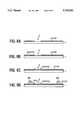
- FIGS. 1A and 1Bare cross-sectional views showing a first, transmission-mode embodiment according to the light modulator of the present invention.
- FIG. 1Ais a cross-sectional side view of the light modulator.
- FIG. 1Bis a top view showing how the shutter plate suspension connects the shutter plate to the spacers.
- FIGS. 2A and 2Bcorrespond to FIGS. 1A and B, and show how the shutter plate moves in response to the drive voltage.
- FIGS. 3A-3Cshow a second, reflection-mode, embodiment of the light modulator according to the present invention.
- FIG. 4A and 4Bshow a third embodiment of the light modulator according to the present invention in which multiple shutter plates are connected in series.
- FIG. 5shows a variation of the light modulator according to the present invention in which the shutter plate is segmented into three parallel plate groups, each plate group composed of multiple, serially-arranged, shutter plate segments.
- FIG. 6shows a fourth embodiment of the light modulator according to the present invention in which the light shielding layer is located on the second substrate, and one of the electrodes is common to all the shutter plates in one cell.
- FIG. 7shows part of a color display composed of multiple light modulators according to the present invention, each light modulator forming a cell of the display.
- the light shielding layeris located on the second substrate, one of the electrodes is common to all the shutter plate segments of the cell, and a color filter chip is located in the window.
- FIGS. 8A-8Dillustrate the process that may be used to fabricate the first substrate assembly.
- FIGS. 9A-9Eillustrate the process that may be used to fabricate the second substrate assembly.
- the light modulator according to the present inventionincludes a substratepair composed of a first substrate placed parallel to a second substrate todefine a cavity between the substrates.
- An opaque light shielding layer defining a translucent windowis formed on one or both substrates.
- the light modulatoradditionally includes a shutter assembly, preferably composed of a polymer material.
- the shutter assemblyincludes a shutter plate and a shutter suspension.
- the shutter plateis located in the cavity, adjacent the translucent window, and is capable of movement parallel to the substrates to overlap the window. The shutter varies the amount of light transmitted between the first substrate and the second substrate, or vice versa, depending on the overlap between the shutter plate and the translucent window.
- the shutter suspensionis elastic and supports the shutter plate in the cavity between the substrates. One end of the shutter suspension is fixed to the substrate pair. The other end of the shutter suspension is attachedto the shutter plate.
- the shutter suspensionmay be composed of two elastic suspension members disposed on opposite sides of the shutter plate in the direction of motionof the shutter plate, for example. One end of each suspension member can befixed to the substrate pair with the other end of each suspension member attached to the shutter plate.
- the shutter platemay be segmented into multiple shutter plate segments.
- the shutter suspensionsupports the whole segmented shutter plate.
- the shutter plate segmentsmay be serially disposed relative to one another in the direction of motion of the shutterplate, or may be disposed parallel to one another, in a direction perpendicular to the direction of motion, or may form an array, with some shutter plate segments disposed in the direction of motion, and others disposed perpendicular to the direction of motion.
- the shutter plate segmentsmay be attached to one another, and the whole segmented shutter plate attached to the suspension members.
- the number of suspension members forming the shutter suspensioncan be increased when appropriate.
- the shutter plateis moved by electrostatic force exerted by at least two electrodes, to be described below. After the shutter plate has been moved, the shuttersuspension generates the force to restore the shutter plate to a mechanically-stable position.
- the mechanically-stable position of the shutter platemay correspond to no overlap between the shutter plate and the translucent window, or alternatively may correspond to a complete overlap between the shutter plate and the translucent window.
- the shutter assemblymay additionally include intervening parts such as spacers that extend between the first substrate and the second substrate and to which the elastic suspension members are fixed.
- the shutter assemblyincluding the shutter plate and the suspension members can be formed as an integral unitwith at least part of the spacers.
- the shutter plateis moved by electrostatic force created by applying a drive voltage to electrodes located on at least two of the following: the shutter assembly, the first substrate, and the second substrate.
- the electrostatic forcemay move the shutter plate by attraction or repulsion.
- the drive voltageis usually a unidirectional pulse.
- the electrodesnormally include a single pair of electrodes, but may include more electrodes than this. Movement of the shutter plate changes the overlap between the shutter plate and the translucent window.
- the shutter suspensionelasticallyrestores the shutter plate to its mechanically-stable position.
- the light modulatorcan be structured so that the shutter plate has approximately zero overlap with the translucent window at the mechanically-stable position.
- applying the drive voltage to the electrodesincreases the overlap.
- a sufficiently high drive voltagewill move the shutter plate to a position where it completely overlaps thewindow.
- the shutter platecan completely overlap the translucent window at its mechanically-stable position.
- applying the drive voltage to the electrodesreduces the overlap.
- a sufficiently high drive voltagewill move the shutter plate to a position where it has approximately zero overlap with the window.
- the first and second substratesare both translucent and the light shielding layer can be formed on one or both of them.
- moving theshutter platechanges the amount of light that passes through the translucent window after passing into the cavity from the second substrateor the first substrate.
- the first substrateis translucent, the light shielding layer is formed on the first substrate, and a light reflecting layer is formed on the inside surface of the secondsubstrate.
- the inside surface of each substrateis the surface of the substrate that faces the other substrate.
- the light reflecting layeris formed on the inside surface of the first substrate. In this variation, light entersand leaves the cavity through the second substrate, which should have a lowreflectivity.
- the cavity between the first and second substrates constituting the substrate pairmay be created by placing spacers between the substrates.
- Multiple light modulators according to the inventionmay be arranged in anarray and may be used to provide a display.
- each individual light modulatorcomposed of at least one shutter assembly and at least two electrodes, will be referred to as a cell.
- Each cellprovidesone pixel of the display.
- the cavitymay belong exclusively to a single cell. Alternatively, the cavity may be common to multiple cells.
- a fluidmay be sealed in the cavity. Filling the cavity with a fluid enables the shutter plate to be moved a given distancerelative to the window using a smaller drive voltage.
- the light modulator according to the inventionmay employ what will be termed a "conductive" shutter plate.
- the resistivity of the material of the shutter plateis less than about 10 10 ⁇ cm.
- the resistivity of the fluidshould be at least ten times greater than that ofthe material of the shutter plate, and in any case should be greater than about 10 7 ⁇ cm.
- the light modulatormay employ what will be termed "conductive" fluid.
- the resistivity of the fluidis less than about 10 10 ⁇ cm.
- the resistivity of the material of the shutter plateshould be at least ten times greater than that of the fluid, and in any case should be greater than about 10 7 ⁇ cm.
- the light modulator according to the inventionmay employ what will be termed a "low dielectric constant" shutter plate.
- the dielectric constant of the material of the shutter plateis less than about five.
- the dielectric constant of the fluidshould be at least twice that of the material of the shutter plate.
- the resistivities of both the fluid and the material of the shutter plateshould be greater than about 10 7 ⁇ cm.
- the light modulator according to the inventionmay employ what will be termed a "high dielectric constant" shutter plate.
- the dielectric constant of the material of the shutter plateisgreater than about five.
- the dielectric constant of the material of the shutter plateshould be at least twice that of the fluid.
- the resistivities of both the fluid and the material of the shutter plateshould be greater than about 10 7 ⁇ cm.
- Arrays of the light modulators according to the inventioncan be used in such devices as monochrome or color displays and overhead projectors.
- a matrix of red, green, and blue trichromatic filterscan be formed on the first or second substrate, one filter for each cell.
- FIG. 1The first embodiment of a light modulator according to the present invention will now be described with reference to FIGS. 1A and 1B. These figures will be collectively referred to as FIG. 1.
- FIG. 1Ashows a side view of the light modulator 100.
- the light modulatormay be a single light modulator, or may be one cell in of an array of light modulators constituting a display.
- the light modulator 100includes a substrate pair composed of the first substrate 1 and the second substrate 2. Spacers, collectively indicated by the reference numeral 8, separate the first substrate from the second substrate to form the cavity 4.
- the spacersmay have the planar rectangular shape shown in FIG. 1B. In FIG. 1, the spacers 8A and 8B are shown as examples of the spacers 8.
- the first and second substrates 1 and 2are both translucent. Each substrate may be a glass plate, but other suitable planar translucent materials may be used. For example, an organic polymer film can be used toreduce weight and provide greater mechanical flexibility.
- a light source(not shown) is located adjacent the second substrate 2, remote from the first substrate 1.
- the opaque light shielding layer 10is formed on the inside surface of the first substrate 1.
- the inside surface of a substrateis the surface of the substrate that faces the other substrate.
- An aperture in the light shielding layerdefines the translucent window 3.
- the light modulator 100constitutes one cell of a display, for example, multiple apertures are formed in the light shielding layer to define an array of windows.
- the substrates 1 and 2define the cavity 4 which is filled with the dielectric fluid L.
- the shutter suspension 6extends between the spacers 8A and 8B and the shutter plate 5.
- the shutter suspension 6is composed of the elastic suspension members 6A and 6B. One end of each suspension member 6A and 6B is fixed to the spacers 8A and 8B, respectively. The other end of each suspension member is attached to the shutter plate.
- the suspension members 6A and 6Bhave a folded-beam structure that makes the shutter suspension compliant in the direction of motion of the shutter plate.
- the shutter suspension 6supports the shutter plate 5 parallel to the substrates 1 and 2 in the cavity 4 and allows the shutter plate to move parallel to the substrates in a direction that changes the overlap between the shutter plate and the window 3.
- the shutter plate 5is formed of an opaque material. As will be discussed in more detail below, the material of the shutter plate may have a resistivity ranging from high to low, and may have a dielectric constant ranging from high to low.
- the width and length of the shutter plate(in the x and y directions shown in FIG. 1B) are slightly larger than the width and length, respectively, of the window 3. Changing the overlap between the shutter plate and the window 3 changes the amount of light transmitted through the window.
- the shutter suspension6holds the shutter plate in a mechanically-stable position where the shutter plate has a zero overlap with the window. However, the shutter suspension is formed to allow the shutter plate to move to a position where the shutter plate completely overlaps the window and prevents light from being transmitted through the window.
- the shutter plate 5is moved from its mechanically-stable position by an electrostatic force exerted by applying a drive voltage to the electrodes 7A and 7B.
- the electrode 7Acovers the window 3 on the inside surface of the first substrate 1.
- the electrode 7Bis located on the inside surface the second substrate 2, opposite the electrode 7A.
- the electrodes 7A and 7Bare both translucent in this embodiment.
- the power source 9is connected between the electrodes. The power source 9 can apply a specific value of the drive voltage Vd between the electrodes to move the shutter plate 5 by electrostatic attraction.
- the light modulator 100preferably requires a drive voltage Vd of less than10 V, and even more preferably requires a drive voltage of less than several volts.
- the value of the drive voltage Vdgreatly depends on the spring constants of the suspension members 6A and 6B.
- the spring constantsof the suspension membersdepend on the coefficient of elasticity of the material of the suspension members, and on the dimensions of the suspension members. Inorganic materials, such as silicon or aluminum, generally have large coefficients of elasticity. Suspension members made of these materials must have cross-sectional dimensions as small as about 0.1 ⁇ m for a drive voltage Vd of less than about 10 V to be used.
- the coefficient of elasticity of organic polymer materialssuch as polyimide or polymethyl methacrylate (PMMA) is usually less than one tenthof that of the above-mentioned inorganic materials. Therefore, the suspension members 6A and 6B are preferably formed using polyimides. This enables the suspension members to have larger cross-sectional dimensions while keeping the drive voltage Vd below about 10 V.
- the suspension members 6A and 6Bare about 1 ⁇ m, the suspension members can be inexpensively formed with a high yield using conventional photolithographic processing employing a contact-type photomask. If a drive voltage somewhat higher than about 10 Vcan be used, the cross-sectional dimensions of the suspension members can be increased beyond 1 ⁇ m. This would allow the suspension members 6A and 6B to be formed using printing techniques that are even lower in cost.
- dielectric fluid Lcan be used as many different liquids.
- An example of a dielectricliquid with such characteristicsis the liquid fluorocarbon sold under the brand name FluorinertTM.
- Dielectric liquids with a dielectric constant of 20 or more at room temperature, such as water, ethanol, methanol, ethylene glycol, and formamidemay also be used.
- a liquid crystalwas used as the fluid L.
- the dielectric fluidLis also used to damp the movement of the shutter plate 5, and therefore must have a viscosity suitable for this purpose. The preferred viscosity depends on a number of factors including the desired response speed of thelight modulator, the spring constant of the shutter suspension, the drive voltage, etc.
- Using a low resistivity liquid, such as water, as the dielectric fluid Lresults in a high leakage current. This results in the equilibrium state of the shutter plate 5 having a short hold time.
- a short hold timeis generally undesirable, and a hold time of some length is usually preferable.
- dielectric fluid LTo obtain the desired combination of resistivity, dielectric constant and viscosity, several different liquids may be mixed to form the dielectric fluid L.
- a conductive polymer materialcan be used as the shutter plate 5.
- the preferred materials of the shutter plateare polyimide or PMMA. Both of these materials normally have a very high resistivity, but the resistivity of these materials can be significantly reduced by injecting carbon or nitrogen ions into the material.
- a conducting layermay be formed in or on the shutter plate 5.
- FIG. 1Bis a top view showing how the suspension members 6A and 6B constituting the shutter suspension 6 connect the shutter plate 5 to the spacers 8A and 8B.
- the suspension membersare formed so that when the drive voltage Vd is 0 V, the shutter suspension holds the shutter plate 5 in a mechanically-stable position where there is no overlap between the shutter plate and the window 3.
- the input light Bin, incident on the second substrate 2passes through the second substrate and into the cavity 4, and then passes through the window and the first substrate 1 as the output light Bout.
- FIG. 1shows the state of the light modulator 100 when the drive voltage Vdis 0V.
- FIGS. 2A and 2Bcollectively referred to as FIG. 2, show the state of the light modulator when the drive voltage is greater than 0V.
- the voltage applied to the electrodes 7A and 7Bhasmoved the shutter plate 5 sufficiently towards the electrodes in the x-direction that the shutter plate completely overlaps the window 3.
- the amount of incident light Bin that passes through the windowis determined by the position of the shutter plate 5 relative to the window.
- either the electrode 7A or the electrode7Bmay be omitted, and the drive voltage Vd applied to the shutter plate 5. If this is done, a relatively conductive material should be used for the shutter plate 5. However, applying the drive voltage to the shutter plate subjects the shutter plate to an electrostatic force in the z direction, perpendicular to the first and second substrates 1 and 2. This force causes friction between the shutter plate and the adjacent substrate, which prevents the shutter plate 5 from moving smoothly.
- the direct drive voltage Vdis not applied directly to the shutter plate 5.
- the electrodes 7A and 7Bapply equal and opposite electrostatic forces to the shutter plate in the z-direction. Consequently, the forces applied to the shutter plate cancel out, and the shutter plate can move smoothly back and forth.
- the material of the shutter plate 5is polyimide that has been modified as described above to make it relatively conductive, and the dielectric fluid L is a liquid crystal having a relatively high dielectric constant.
- the material of the shutter plate 5may alternatively have a relatively high dielectric constant. In this case, the shutter plate 5 can be moved by electrostatic attraction as described above if the dielectric fluid has a smaller dielectric constant than that of the material of the shutter plate.
- the shutter plate 5can alternatively be constructed from a material havinga relatively low dielectric material, and the dielectric fluid L can be a liquid having a greater dielectric constant than that of the material of the shutter plate.
- the shutter plateis moved by electrostatic repulsion.
- the shutter suspension 6is configured to have a mechanically-stable position in which the shutter plate is located at the position shown in FIG. 2. Increasing the drive voltage Vd from 0 V moves the shutter plate in the -x direction away from the electrodes 7A and 7B until the shutter plate reaches the position shown in FIG. 1.
- the shutter plate 5can be formed froma material having a low conductivity, and the dielectric fluid L can have agreater conductivity greater than that of the shutter plate. In this case, the shutter plate 5 is moved by electrostatic repulsion. However, to prevent current from flowing between the electrodes 7A and 7B, the electrodes must be covered with a thin insulating film. In addition, when the light modulator constitutes a cell in an array of cells constituting adisplay, the cavity of the cell must be insulated from the cavities of neighboring cells to prevent interaction between neighboring cells.
- the spacers 8may serve as suitable insulators, for example.
- FIGS. 3A-3Cshow a second embodiment of the light modulator according to the present invention.
- the embodiment shown FIG. 3operates by reflection.
- the incident light Binpasses throughthe window 3 into the cavity 4, and is reflected by a light-reflective layer formed on the second substrate 2.
- the fraction of the incident lightthat is reflectedis changed by the position of the shutter plate 5.
- the reflected lightpasses back through the window 3 as the output light Bout.
- the electrode 7B' on the second substrate 2serves as the reflective layer in the light modulator shown in FIG. 3.
- the electrode 7B'is a layer of a conductive material having a high reflectivity, such as aluminum.
- the material of the shutter plate 5has a low transmissivity and reflectivity,and preferably contains a black pigment.
- the fraction of the incident light Bin reflected as the output light Boutis changed by changing the position of the shutter plate 5. Specifically, when the shutter plate 5 is in the position shown in FIG. 3A, the shutter plate blocks none of the incident light Bin from reaching the reflective electrode 7B', and the fraction of the incident light Bin reflected as the output light Bout is close to 100%. When the shutter plate is in the position shown in FIG. 3B, the shutter plate blocks a portion of the incident light Bin from reaching thereflective electrode 7B', and reflective electrode reflects the fraction ofthe incident light Bin that is not blocked as the output light Bout. When the shutter plate is in the position shown in FIG. 3C, the shutter plate 5blocks all of the incident light Bin from reaching the reflective electrode, and none of the incident light is reflected as the output lightBout.
- the efficiency of the light modulator described abovedepends on the ratio of the area of the window 3 to the area of the first substrate 1 or the second substrate 2 occupied by the cell. This ratio will be called the aperture ratio.
- the efficiency of the light modulatoris increased by increasing the aperture ratio, which, in turn, is increased by increasing the area of the window relative to the area of the cell.
- Increasing the area of the window 3 to increase the aperture ratiorequires that the areaof the shutter plate 5 also be increased. This increases the distance that the shutter plate 5 must move, which increases the drive voltage Vd.
- thinner suspension members 6A and 6Bit may be necessary to use thinner suspension members 6A and 6B. However, as discussed above, thinner suspension members are more expensive to produce.
- FIGS. 4A and 4Bcollectively referred to as FIG. 4, show a third embodiment of the light modulator according to the invention.
- the area of the window 3is increased without the problems just described by dividing the shutter plate into multiple, serially-connected, shutter plate segments.
- the window 3is divided into multiple window segments, each corresponding to one of the shutter plate segments; and each of the electrodes 7A and 7B is divided into multiple, electrically-interconnected electrode segments, each corresponding to one of the shutter segments.
- the shutter plate 5is divided into the three shutter plate segments 51, 52 and 53, and the window and the electrodes are therefore each divided into three segments, each corresponding to one of the shutterplate segments.
- the size of one pixelis roughly 200 ⁇ m ⁇ 200 ⁇ m.
- a high-resolution display using an array of light modulators similar to the embodiment shown in FIG. 4if the size ofeach of the windows 3 is 10 ⁇ m ⁇ 200 ⁇ m, then a cell using ten, serially-arranged shutter plates 5 will provide a pixel of roughly 200 ⁇ m ⁇ 200 ⁇ m.
- a shutter plate composed of multiple, serially-connected shutter plate segments 51-53instead of one large shutter plate has the following advantages.
- the electrostatic force applied to the shutter plateis substantially proportional to the number of shutter plate segments, the electrostatic force applied to a shutter plate composed of n serially-connected shutter plate segments for a given drive voltage Vd is n times the force applied to a single shutter plate of the same area. This has the advantage of further lowering the drive voltage Vd, or allowing the cross-sectional dimensions of the suspension members 6A and 6B to be increased.
- FIG. 5shows the shutter plate 5, suspension members 61A, 61B, 61C and 61D, and spacers 8 of a variation on the third embodiment of the light modulator according to the invention.
- the shutter plateis divided into 13 shutter plate segments arranged in three shutter plate groups 5A, 5B and 5C.
- the shutter plate groupsare disposed parallel to one another.
- the shutter plate segments forming each shutter plate groupare serially interconnected in a fixed spatial relationship.
- the shutter plate groups 5A, 5B and 5Care composed of the shutter plate segments 5A, to 5A 4 , 5B 1 to 5B 5 , and 5C 1 to 5C 4 , respectively.
- the shutter plate groups 5A-5Care interconnected in parallel in a fixed spatial relationship to form the shutter plate 5.
- the shutter plate 5is connected to the spacers 8 by the suspension members 61A-61D installed at appropriate positions.
- the spacers 8C and 8Dare shown as examples of the spacers 8.
- two suspension members 61A and 61Bare connected to the shutter plate segment 5B 1 and the suspension members 61C and 61C are connected to the shutter plate segments 5A 4 and 5C 4 , respectively.
- all the electrode segments on the first substrateare electrically connected to one another, and all the electrodesegments on the second substrate are electrically connected to one another,similar to the electrode segments shown in FIG. 4.
- a light modulator using the shutter plate shown in FIG. 5, composed of the shutter plate groups 5A-5C, the suspension members 61A-61D, and the corresponding segmented electrodes and segmented windowsmay be used as a cell constituting one pixel of a display.
- the light modulator shown in FIG. 1is assembled by joining together a first substrate assembly and a second substrate assembly.
- the first substrate assemblyis composed of the first substrate 1, on which are mounted a first portion of each of the spacers 8A and 8B, the light shielding layer 10, and the electrode 7A.
- the second substrate assemblyis composed of the second substrate 2, on which are mounted the remaining second portion of each of the spacers 8A and 8B, the shutter suspension 6, the shutter plate 5, and the electrode 7B.
- FIG. 6A fourth embodiment of the light modulator according to the invention that eliminates the above problem is shown in FIG. 6.
- the embodiment shown in FIG. 6has the same segmented shutter plate 5 as in the embodiment shown in FIG. 4.
- the light shielding layer 10is formed on the inside surface of the second substrate 2, and the electrode 7A is reflective, andis not segmented. Instead, a continuous, extended electrode 7A is common toall the shutter plate segments 51, 52 and 53.
- the electrode 7A on the first substrate 1can be made common to all the shutter plate segments 51, 52, 53, . . . in the cell.
- the electrode 7A on the first substratecan be made common to all of the cells in the display, or to a subset of all the cells.
- the electrodes 7A and 7Bare asymmetrical, irrespective of whether the electrode 7A is common to the shutter plate segments of one cell or is common to the shutter plate segments of multiple cells. Fringe effects caused by the asymmetrical electrodes generate an electrostatic force in the z direction. However, this electrostatic force is usually small, so the effect of this force on the shutter plate 5 can be counteracted by increasing the rigidity of the shutter suspension 6 in the z direction.
- each shutter plate 5, or each shutter plate groupcan be driven directly by its own individual driver since the number of pixels is extremely small.
- the drive methodis basically the same as the matrix drive circuit used in a twisted nematic (TN) liquid crystal display.
- TNtwisted nematic
- each shutter plate 5can bedirectly driven by a matrix circuit.
- each shutter plate 5can be driven by inserting the nonlinear elements, such as transistors or diodes, as areoften used in liquid crystal displays, between the electrodes 7A and 7B anda matrix circuit.
- Driving liquid crystal displays with a prolonged unidirectional voltagecandegrade the characteristics of the display.
- a voltage drive whose polarity periodically reversesis therefore preferred to prevent the characteristics of the display from being degraded. This makes the drive circuit complex, and can easily generate flicker.
- a display based on the light modulators according to the present inventionis designed to be driven using a unidirectional voltage, so deterioration similar to that which can occur in a liquid crystal display does not occur, the drive circuit is simplified, and flicker is less likely to occur.
- the light modulators described abovecan be applied to monochrome displays with the light source being ambient lighting, such as indoor lighting or natural lighting, or artificial lighting (backlighting), or to color displays that use artificial lighting.
- the transmitted light or reflected light that is modulated in a two dimensional array in a monochrome displayforms an image corresponding to the signal generated by the drive circuit.
- an array of trichromatic red (R), green (G), and blue (B) filter chipsmay be arranged on the surface of the first substrate 1 or the second substrate 2, with one filter chip corresponding to each cell.
- FIG. 7shows an example of part of a transmission-mode color display incorporating three light modulators according to the invention.
- FIG. 7shows an arrangement of three cells. In each cell, a different one of a red (R) filter chip 141, a green (G) filter chip 142 and a blue (B) filterchip 143 covers the window 3 of the cell.
- the translucent electrode 7Ais common to the three cells, and may be common to all the cells constitutingthe display.
- Each cellincludes the transparent electrode 7B connected to the thin-film transistor (TFT) 11.
- the TFTselectively connects the drive voltage to the electrode 7B.
- the electrodes of the TFT of the cell having the red filter chip 141are indicated by the reference numerals 111-113.
- the light sourceis composed of the light-conducting shutter plate 12 and the fluorescent lamp 13.
- the light Bin from the light-conducting shutter plateis incident on the second substrate 2.
- the spacersare indicated by reference numeral 8.
- the shutter suspension of the cell having the red filter chipare indicated by the reference numeral 6.
- the color filter chips 141-143can be formed and can be mounted on the substrate I using the same technology used form forming and mounting such filters in conventional color liquid crystal displays. Accordingly, the method of forming and mounting the color filters will not be described in detail.
- the light modulator of the present inventionmay be combined with an optical system and can be applied to a projection display such as an overhead projector.
- the light modulator described abovecan easily be made using micro-lithography or printing, depending on the circumstances.
- the light modulatoris a transmission-mode light modulator, and is one of multiple light modulators constituting the cells of a display having a simple matrix drive. Fabrication of a single light modulator willbe described. In practice, all of the light modulators constituting the display are made simultaneously using common processing.
- the first substrate 1is a sheet of glass about 1 mm thick.
- a layer of chromium about 1,000 ⁇ thickis deposited on one surface of the first substrate to provide the light shielding layer 10. Parts of the layer of chromium is removed to form the window 3, as shown in FIG. 8A.
- a layer of SiO 2 about 1,000 ⁇ thickis next deposited, as shown in FIG. 8B.
- ITOindium tin oxide
- a layer of polyimide about 3 ⁇ m thickis deposited. Parts of the polyimide layer are selectively remove to form the 1.5 ⁇ m-thick first spacer portions 8X, as shown in FIG. 8D.
- the second substrate 2is a sheet of glass about 1 mm thick.
- a layer of indium tin oxide (ITO) about 1,000 ⁇ thickis deposited on one surface of the second substrate. Parts of the ITO layer are selectively removed to define the electrode 7B, as shown in FIG. 9A.
- ITOindium tin oxide
- the second substrateis coated with a layer of resist about 1.5 ⁇ mthick, and holes through which the second spacer portions 8Y will contact the second substrate are opened in the resist, as shown in FIG. 9B.
- the second substrateis next coated with a layer of a photosensitive polyimide about 6 ⁇ m thick, as shown in FIG. 9C.
- the polyimide usedcontains a black pigment and has a dielectric constant of about 3.
- the second substrateis then heat treated to drive off solvents in the polyimide. This reduces the thickness of the polyimide layer to the required 3 ⁇ m.
- step (2-e)The remainder of the layer of resist coated in step (2-b) is removed.This leaves the shutter plate 5 connected to the second spacer portions 8Y by the shutter suspension 6. The shutter plate and the shutter suspension are separated from the second substrate by the thickness of the removed resist layer, as shown in FIG. 9E.
- the first substrate assembly and the second substrate assembly, fabricated as described above,are bonded together so that the surfaces of the first and second substrates on which the components are formed face one another.
- the lateral positions of the substrate assembliesare set so that each of the first spacer portions 8X mate with its corresponding second spacer portion 8Y to form one of the spacers 8.
- liquid crystal with a dielectric constant of 25is injected into the cavity 4 created by the spacers between the substrates. Complete filling of the cavity 4 can be ensured by bonding the first substrate assembly and the second substrate while the substrates are immersed in a bath of the liquid crystal.
- the light modulator according to the present invention and having one of the structures described abovecan be applied to two-dimensional filters for various electromagnetic waves, two-dimensional light modulators, and two-dimensional optical computers so that such devices can be made using asimple structure not possible before.
- the light modulator according to the present inventioncan used as a cell of a display.
- Using the light modulator according to the invention in a displayconfers on such a display the main advantages of both cathode ray tubes and liquid crystal displays without their attendantdisadvantages.
Landscapes
- Physics & Mathematics (AREA)
- General Physics & Mathematics (AREA)
- Engineering & Computer Science (AREA)
- Optics & Photonics (AREA)
- Theoretical Computer Science (AREA)
- Nonlinear Science (AREA)
- Ceramic Engineering (AREA)
- Crystallography & Structural Chemistry (AREA)
- Chemical & Material Sciences (AREA)
- Mechanical Light Control Or Optical Switches (AREA)
- Devices For Indicating Variable Information By Combining Individual Elements (AREA)
- Liquid Crystal (AREA)
- Electrochromic Elements, Electrophoresis, Or Variable Reflection Or Absorption Elements (AREA)
Abstract
Description
Claims (20)
Applications Claiming Priority (2)
| Application Number | Priority Date | Filing Date | Title |
|---|---|---|---|
| JP7-352615 | 1995-12-29 | ||
| JP35261595AJP3799092B2 (en) | 1995-12-29 | 1995-12-29 | Light modulation device and display device |
Publications (1)
| Publication Number | Publication Date |
|---|---|
| US5745281Atrue US5745281A (en) | 1998-04-28 |
Family
ID=18425264
Family Applications (1)
| Application Number | Title | Priority Date | Filing Date |
|---|---|---|---|
| US08/771,566Expired - Fee RelatedUS5745281A (en) | 1995-12-29 | 1996-12-20 | Electrostatically-driven light modulator and display |
Country Status (4)
| Country | Link |
|---|---|
| US (1) | US5745281A (en) |
| EP (1) | EP0786679A3 (en) |
| JP (1) | JP3799092B2 (en) |
| KR (1) | KR970048702A (en) |
Cited By (265)
| Publication number | Priority date | Publication date | Assignee | Title |
|---|---|---|---|---|
| US6191883B1 (en)* | 1998-12-30 | 2001-02-20 | Texas Instruments Incorporated | Five transistor SRAM cell for small micromirror elements |
| US6249370B1 (en)* | 1998-09-18 | 2001-06-19 | Ngk Insulators, Ltd. | Display device |
| US6275320B1 (en)* | 1999-09-27 | 2001-08-14 | Jds Uniphase, Inc. | MEMS variable optical attenuator |
| US6288824B1 (en)* | 1998-11-03 | 2001-09-11 | Alex Kastalsky | Display device based on grating electromechanical shutter |
| US6296383B1 (en)* | 1996-04-17 | 2001-10-02 | Dicon A/S | Method and apparatus for controlling light |
| US6327071B1 (en)* | 1998-10-16 | 2001-12-04 | Fuji Photo Film Co., Ltd. | Drive methods of array-type light modulation element and flat-panel display |
| WO2001096928A1 (en)* | 2000-06-09 | 2001-12-20 | University Of Hawaii | Mems optical components |
| US6356254B1 (en)* | 1998-09-25 | 2002-03-12 | Fuji Photo Film Co., Ltd. | Array-type light modulating device and method of operating flat display unit |
| US20020075555A1 (en)* | 1994-05-05 | 2002-06-20 | Iridigm Display Corporation | Interferometric modulation of radiation |
| US6495944B2 (en) | 2001-04-18 | 2002-12-17 | International Business Machines Corporation | Electrostatic microactuator with viscous liquid damping |
| US6538796B1 (en)* | 2000-03-31 | 2003-03-25 | The United States Of America As Represented By The Administrator Of The National Aeronautics And Space Administration | MEMS device for spacecraft thermal control applications |
| US6560002B2 (en)* | 2000-11-15 | 2003-05-06 | Japan Aviation Electronics Industry, Limited | Optical switch |
| US6574032B1 (en)* | 2002-01-23 | 2003-06-03 | Eastman Kodak Company | Imaging apparatus using dither to minimize pixel effects |
| US20030202265A1 (en)* | 2002-04-30 | 2003-10-30 | Reboa Paul F. | Micro-mirror device including dielectrophoretic liquid |
| US20030202266A1 (en)* | 2002-04-30 | 2003-10-30 | Ring James W. | Micro-mirror device with light angle amplification |
| US6667823B2 (en)* | 2002-05-22 | 2003-12-23 | Lucent Technologies Inc. | Monolithic in-plane shutter switch |
| US20040160143A1 (en)* | 2003-02-14 | 2004-08-19 | Shreeve Robert W. | Micro-mirror device with increased mirror tilt |
| US20040165162A1 (en)* | 2003-02-24 | 2004-08-26 | Eastman Kodak Company | Method and apparatus for translating a spatial light modulator to provide dithering |
| US20040179281A1 (en)* | 2003-03-12 | 2004-09-16 | Reboa Paul F. | Micro-mirror device including dielectrophoretic liquid |
| US20040179773A1 (en)* | 2003-03-13 | 2004-09-16 | Aksyuk Vladimir A. | Waveguide/MEMS switch |
| US20040233503A1 (en)* | 2003-05-23 | 2004-11-25 | Fuji Photo Film Co., Ltd. | Transmissive spatial light modulator and method of manufacturing the same |
| US20040240032A1 (en)* | 1994-05-05 | 2004-12-02 | Miles Mark W. | Interferometric modulation of radiation |
| US20040263944A1 (en)* | 2003-06-24 | 2004-12-30 | Miles Mark W. | Thin film precursor stack for MEMS manufacturing |
| US6859299B1 (en) | 1999-06-11 | 2005-02-22 | Jung-Chih Chiao | MEMS optical components |
| US6876484B2 (en) | 2003-03-24 | 2005-04-05 | Lucent Technologies Inc. | Deformable segmented MEMS mirror |
| US20050073736A1 (en)* | 2003-10-02 | 2005-04-07 | James Guo | Micro mirror device with spring and method for the same |
| US20050122559A1 (en)* | 2003-12-09 | 2005-06-09 | Reboa Paul F. | Light modulator |
| US20050122560A1 (en)* | 2003-12-09 | 2005-06-09 | Sampsell Jeffrey B. | Area array modulation and lead reduction in interferometric modulators |
| US20050152017A1 (en)* | 2002-04-30 | 2005-07-14 | Reboa Paul F. | Micro-mirror device including dielectrophoretic microemulsion |
| US20050168431A1 (en)* | 2004-02-03 | 2005-08-04 | Clarence Chui | Driver voltage adjuster |
| US20050195464A1 (en)* | 2004-03-05 | 2005-09-08 | Kenneth Faase | Micro mirror device with adjacently suspended spring and method for the same |
| US20050212738A1 (en)* | 2004-03-06 | 2005-09-29 | Brian Gally | Method and system for color optimization in a display |
| US20050243921A1 (en)* | 2004-03-26 | 2005-11-03 | The Hong Kong University Of Science And Technology | Efficient multi-frame motion estimation for video compression |
| US20050247477A1 (en)* | 2004-05-04 | 2005-11-10 | Manish Kothari | Modifying the electro-mechanical behavior of devices |
| US20050254115A1 (en)* | 2004-05-12 | 2005-11-17 | Iridigm Display Corporation | Packaging for an interferometric modulator |
| US20050270613A1 (en)* | 2003-05-29 | 2005-12-08 | Asml Holding N.V. | System and method for dose control in a lithographic system |
| US20050277277A1 (en)* | 2000-10-13 | 2005-12-15 | Taiwan Semiconductor Manufacturing Company, Ltd. | Dual damascene process |
| US20050286114A1 (en)* | 1996-12-19 | 2005-12-29 | Miles Mark W | Interferometric modulation of radiation |
| US20050286113A1 (en)* | 1995-05-01 | 2005-12-29 | Miles Mark W | Photonic MEMS and structures |
| US20060001942A1 (en)* | 2004-07-02 | 2006-01-05 | Clarence Chui | Interferometric modulators with thin film transistors |
| US20060025146A1 (en)* | 2002-10-18 | 2006-02-02 | Gallagher Michael D | Architecture of an unlicensed wireless communication system with a generic access point |
| US20060044928A1 (en)* | 2004-08-27 | 2006-03-02 | Clarence Chui | Drive method for MEMS devices |
| US7012726B1 (en) | 2003-11-03 | 2006-03-14 | Idc, Llc | MEMS devices with unreleased thin film components |
| US20060056004A1 (en)* | 2004-09-14 | 2006-03-16 | Adel Jilani | Flexure |
| US20060057754A1 (en)* | 2004-08-27 | 2006-03-16 | Cummings William J | Systems and methods of actuating MEMS display elements |
| US20060066560A1 (en)* | 2004-09-27 | 2006-03-30 | Gally Brian J | Systems and methods of actuating MEMS display elements |
| US20060067641A1 (en)* | 2004-09-27 | 2006-03-30 | Lauren Palmateer | Method and device for packaging a substrate |
| US20060067652A1 (en)* | 2004-09-27 | 2006-03-30 | Cummings William J | Methods for visually inspecting interferometric modulators for defects |
| US20060066557A1 (en)* | 2004-09-27 | 2006-03-30 | Floyd Philip D | Method and device for reflective display with time sequential color illumination |
| US20060065043A1 (en)* | 2004-09-27 | 2006-03-30 | William Cummings | Method and system for detecting leak in electronic devices |
| US20060066871A1 (en)* | 2004-09-27 | 2006-03-30 | William Cummings | Process control monitors for interferometric modulators |
| US20060066542A1 (en)* | 2004-09-27 | 2006-03-30 | Clarence Chui | Interferometric modulators having charge persistence |
| US20060066559A1 (en)* | 2004-09-27 | 2006-03-30 | Clarence Chui | Method and system for writing data to MEMS display elements |
| US20060066541A1 (en)* | 2004-09-27 | 2006-03-30 | Gally Brian J | Method and device for manipulating color in a display |
| US20060066598A1 (en)* | 2004-09-27 | 2006-03-30 | Floyd Philip D | Method and device for electrically programmable display |
| US20060066938A1 (en)* | 2004-09-27 | 2006-03-30 | Clarence Chui | Method and device for multistate interferometric light modulation |
| US20060066937A1 (en)* | 2004-09-27 | 2006-03-30 | Idc, Llc | Mems switch with set and latch electrodes |
| US20060066503A1 (en)* | 2004-09-27 | 2006-03-30 | Sampsell Jeffrey B | Controller and driver features for bi-stable display |
| US20060065436A1 (en)* | 2004-09-27 | 2006-03-30 | Brian Gally | System and method for protecting microelectromechanical systems array using back-plate with non-flat portion |
| US20060066600A1 (en)* | 2004-09-27 | 2006-03-30 | Lauren Palmateer | System and method for display device with reinforcing substance |
| US20060067600A1 (en)* | 2004-09-27 | 2006-03-30 | Gally Brian J | Display element having filter material diffused in a substrate of the display element |
| US20060066936A1 (en)* | 2004-09-27 | 2006-03-30 | Clarence Chui | Interferometric optical modulator using filler material and method |
| US20060066594A1 (en)* | 2004-09-27 | 2006-03-30 | Karen Tyger | Systems and methods for driving a bi-stable display element |
| US20060067633A1 (en)* | 2004-09-27 | 2006-03-30 | Gally Brian J | Device and method for wavelength filtering |
| US20060067642A1 (en)* | 2004-09-27 | 2006-03-30 | Karen Tyger | Method and device for providing electronic circuitry on a backplate |
| US20060066597A1 (en)* | 2004-09-27 | 2006-03-30 | Sampsell Jeffrey B | Method and system for reducing power consumption in a display |
| US20060067648A1 (en)* | 2004-09-27 | 2006-03-30 | Clarence Chui | MEMS switches with deforming membranes |
| US20060066863A1 (en)* | 2004-09-27 | 2006-03-30 | Cummings William J | Electro-optical measurement of hysteresis in interferometric modulators |
| US20060072187A1 (en)* | 2004-10-05 | 2006-04-06 | Mckinnell James | Systems and methods for amorphous flexures in micro-electro mechanical systems |
| US20060077512A1 (en)* | 2004-09-27 | 2006-04-13 | Cummings William J | Display device having an array of spatial light modulators with integrated color filters |
| US20060079098A1 (en)* | 2004-09-27 | 2006-04-13 | Floyd Philip D | Method and system for sealing a substrate |
| US20060077527A1 (en)* | 2004-09-27 | 2006-04-13 | Cummings William J | Methods and devices for inhibiting tilting of a mirror in an interferometric modulator |
| US20060077393A1 (en)* | 2004-09-27 | 2006-04-13 | Gally Brian J | System and method for implementation of interferometric modulator displays |
| US20060077524A1 (en)* | 2004-09-27 | 2006-04-13 | Lauren Palmateer | System and method for display device with end-of-life phenomena |
| US20060076634A1 (en)* | 2004-09-27 | 2006-04-13 | Lauren Palmateer | Method and system for packaging MEMS devices with incorporated getter |
| US20060077122A1 (en)* | 2004-09-27 | 2006-04-13 | Gally Brian J | Apparatus and method for reducing perceived color shift |
| US20060077503A1 (en)* | 2004-09-27 | 2006-04-13 | Lauren Palmateer | System and method of providing MEMS device with anti-stiction coating |
| US20060077523A1 (en)* | 2004-09-27 | 2006-04-13 | Cummings William J | Electrical characterization of interferometric modulators |
| US20060077514A1 (en)* | 2004-09-27 | 2006-04-13 | Sampsell Jeffrey B | System and method of reducing color shift in a display |
| US20060077149A1 (en)* | 2004-09-27 | 2006-04-13 | Gally Brian J | Method and device for manipulating color in a display |
| US20060077126A1 (en)* | 2004-09-27 | 2006-04-13 | Manish Kothari | Apparatus and method for arranging devices into an interconnected array |
| US20060103643A1 (en)* | 2004-09-27 | 2006-05-18 | Mithran Mathew | Measuring and modeling power consumption in displays |
| US20060103613A1 (en)* | 2004-09-27 | 2006-05-18 | Clarence Chui | Interferometric modulator array with integrated MEMS electrical switches |
| US20060114438A1 (en)* | 2003-05-29 | 2006-06-01 | Asml Holding N.V. | Maskless lithography systems and methods utilizing spatial light modulator arrays |
| US7119945B2 (en) | 2004-03-03 | 2006-10-10 | Idc, Llc | Altering temporal response of microelectromechanical elements |
| US7123216B1 (en) | 1994-05-05 | 2006-10-17 | Idc, Llc | Photonic MEMS and structures |
| US20060250335A1 (en)* | 2005-05-05 | 2006-11-09 | Stewart Richard A | System and method of driving a MEMS display device |
| US7138984B1 (en) | 2001-06-05 | 2006-11-21 | Idc, Llc | Directly laminated touch sensitive screen |
| US7142346B2 (en) | 2003-12-09 | 2006-11-28 | Idc, Llc | System and method for addressing a MEMS display |
| US20060274400A1 (en)* | 1995-11-06 | 2006-12-07 | Miles Mark W | Method and device for modulating light with optical compensation |
| US20060277486A1 (en)* | 2005-06-02 | 2006-12-07 | Skinner David N | File or user interface element marking system |
| US7161730B2 (en) | 2004-09-27 | 2007-01-09 | Idc, Llc | System and method for providing thermal compensation for an interferometric modulator display |
| US7172915B2 (en) | 2003-01-29 | 2007-02-06 | Qualcomm Mems Technologies Co., Ltd. | Optical-interference type display panel and method for making the same |
| US20070042524A1 (en)* | 2005-08-19 | 2007-02-22 | Lior Kogut | MEMS devices having support structures with substantially vertical sidewalls and methods for fabricating the same |
| US20070047900A1 (en)* | 2005-07-22 | 2007-03-01 | Sampsell Jeffrey B | MEMS devices having support structures and methods of fabricating the same |
| US20070053652A1 (en)* | 2005-09-02 | 2007-03-08 | Marc Mignard | Method and system for driving MEMS display elements |
| US20070058095A1 (en)* | 1994-05-05 | 2007-03-15 | Miles Mark W | System and method for charge control in a MEMS device |
| US7193768B2 (en) | 2003-08-26 | 2007-03-20 | Qualcomm Mems Technologies, Inc. | Interference display cell |
| US7198973B2 (en) | 2003-04-21 | 2007-04-03 | Qualcomm Mems Technologies, Inc. | Method for fabricating an interference display unit |
| US20070086078A1 (en)* | 2005-02-23 | 2007-04-19 | Pixtronix, Incorporated | Circuits for controlling display apparatus |
| US20070147688A1 (en)* | 2005-12-22 | 2007-06-28 | Mithran Mathew | System and method for power reduction when decompressing video streams for interferometric modulator displays |
| US7250315B2 (en) | 2002-02-12 | 2007-07-31 | Idc, Llc | Method for fabricating a structure for a microelectromechanical system (MEMS) device |
| US20070177129A1 (en)* | 2006-01-06 | 2007-08-02 | Manish Kothari | System and method for providing residual stress test structures |
| US20070195026A1 (en)* | 2005-02-23 | 2007-08-23 | Pixtronix, Incorporated | Display methods and apparatus |
| US20070223080A1 (en)* | 2005-02-23 | 2007-09-27 | Pixtronix, Inc. | Methods and apparatus for actuating displays |
| US20070247704A1 (en)* | 2006-04-21 | 2007-10-25 | Marc Mignard | Method and apparatus for providing brightness control in an interferometric modulator (IMOD) display |
| US7289259B2 (en) | 2004-09-27 | 2007-10-30 | Idc, Llc | Conductive bus structure for interferometric modulator array |
| US7291921B2 (en) | 2003-09-30 | 2007-11-06 | Qualcomm Mems Technologies, Inc. | Structure of a micro electro mechanical system and the manufacturing method thereof |
| US7297471B1 (en) | 2003-04-15 | 2007-11-20 | Idc, Llc | Method for manufacturing an array of interferometric modulators |
| US7302157B2 (en) | 2004-09-27 | 2007-11-27 | Idc, Llc | System and method for multi-level brightness in interferometric modulation |
| US7304784B2 (en) | 2004-09-27 | 2007-12-04 | Idc, Llc | Reflective display device having viewable display on both sides |
| US7310179B2 (en) | 2004-09-27 | 2007-12-18 | Idc, Llc | Method and device for selective adjustment of hysteresis window |
| US20070290961A1 (en)* | 2006-06-15 | 2007-12-20 | Sampsell Jeffrey B | Method and apparatus for low range bit depth enhancement for MEMS display architectures |
| US20080002210A1 (en)* | 2006-06-30 | 2008-01-03 | Kostadin Djordjev | Determination of interferometric modulator mirror curvature and airgap variation using digital photographs |
| US7317568B2 (en) | 2004-09-27 | 2008-01-08 | Idc, Llc | System and method of implementation of interferometric modulators for display mirrors |
| US7321457B2 (en) | 2006-06-01 | 2008-01-22 | Qualcomm Incorporated | Process and structure for fabrication of MEMS device having isolated edge posts |
| US7321456B2 (en) | 2004-09-27 | 2008-01-22 | Idc, Llc | Method and device for corner interferometric modulation |
| US20080025849A1 (en)* | 2006-07-31 | 2008-01-31 | Hitachi, Ltd. | High-Pressure Fuel Pump Control Apparatus for an Internal Combustion Engine |
| US7327510B2 (en) | 2004-09-27 | 2008-02-05 | Idc, Llc | Process for modifying offset voltage characteristics of an interferometric modulator |
| US20080030827A1 (en)* | 2005-02-23 | 2008-02-07 | Pixtronix, Inc. | Display methods and apparatus |
| US20080037104A1 (en)* | 2005-02-23 | 2008-02-14 | Pixtronix, Inc. | Alignment methods in fluid-filled MEMS displays |
| US7343080B2 (en) | 2004-09-27 | 2008-03-11 | Idc, Llc | System and method of testing humidity in a sealed MEMS device |
| US20080062500A1 (en)* | 2005-02-23 | 2008-03-13 | Pixtronix, Inc. | Methods and apparatus for spatial light modulation |
| US7349139B2 (en) | 2004-09-27 | 2008-03-25 | Idc, Llc | System and method of illuminating interferometric modulators using backlighting |
| US7349136B2 (en) | 2004-09-27 | 2008-03-25 | Idc, Llc | Method and device for a display having transparent components integrated therein |
| US20080094853A1 (en)* | 2006-10-20 | 2008-04-24 | Pixtronix, Inc. | Light guides and backlight systems incorporating light redirectors at varying densities |
| US20080094686A1 (en)* | 2006-10-19 | 2008-04-24 | U Ren Gregory David | Sacrificial spacer process and resultant structure for MEMS support structure |
| US7369294B2 (en) | 2004-09-27 | 2008-05-06 | Idc, Llc | Ornamental display device |
| US7369292B2 (en) | 2006-05-03 | 2008-05-06 | Qualcomm Mems Technologies, Inc. | Electrode and interconnect materials for MEMS devices |
| US7369296B2 (en) | 2004-09-27 | 2008-05-06 | Idc, Llc | Device and method for modifying actuation voltage thresholds of a deformable membrane in an interferometric modulator |
| US7373026B2 (en) | 2004-09-27 | 2008-05-13 | Idc, Llc | MEMS device fabricated on a pre-patterned substrate |
| US7372613B2 (en) | 2004-09-27 | 2008-05-13 | Idc, Llc | Method and device for multistate interferometric light modulation |
| US7382515B2 (en) | 2006-01-18 | 2008-06-03 | Qualcomm Mems Technologies, Inc. | Silicon-rich silicon nitrides as etch stops in MEMS manufacture |
| US7385744B2 (en) | 2006-06-28 | 2008-06-10 | Qualcomm Mems Technologies, Inc. | Support structure for free-standing MEMS device and methods for forming the same |
| US20080158635A1 (en)* | 2005-02-23 | 2008-07-03 | Pixtronix, Inc. | Display apparatus and methods for manufacture thereof |
| USRE40436E1 (en) | 2001-08-01 | 2008-07-15 | Idc, Llc | Hermetic seal and method to create the same |
| US7405863B2 (en) | 2006-06-01 | 2008-07-29 | Qualcomm Mems Technologies, Inc. | Patterning of mechanical layer in MEMS to reduce stresses at supports |
| US7405924B2 (en) | 2004-09-27 | 2008-07-29 | Idc, Llc | System and method for protecting microelectromechanical systems array using structurally reinforced back-plate |
| US7405861B2 (en) | 2004-09-27 | 2008-07-29 | Idc, Llc | Method and device for protecting interferometric modulators from electrostatic discharge |
| US20080201665A1 (en)* | 2007-02-15 | 2008-08-21 | Teac Corporation | Electronic equipment having plural function keys |
| US7417784B2 (en) | 2006-04-19 | 2008-08-26 | Qualcomm Mems Technologies, Inc. | Microelectromechanical device and method utilizing a porous surface |
| US7417783B2 (en) | 2004-09-27 | 2008-08-26 | Idc, Llc | Mirror and mirror layer for optical modulator and method |
| US7417735B2 (en) | 2004-09-27 | 2008-08-26 | Idc, Llc | Systems and methods for measuring color and contrast in specular reflective devices |
| US7420728B2 (en) | 2004-09-27 | 2008-09-02 | Idc, Llc | Methods of fabricating interferometric modulators by selectively removing a material |
| US7420725B2 (en) | 2004-09-27 | 2008-09-02 | Idc, Llc | Device having a conductive light absorbing mask and method for fabricating same |
| US7450295B2 (en) | 2006-03-02 | 2008-11-11 | Qualcomm Mems Technologies, Inc. | Methods for producing MEMS with protective coatings using multi-component sacrificial layers |
| US20080278798A1 (en)* | 2005-02-23 | 2008-11-13 | Pixtronix, Inc. | MEMs display apparatus |
| US7453579B2 (en) | 2004-09-27 | 2008-11-18 | Idc, Llc | Measurement of the dynamic characteristics of interferometric modulators |
| US20080283175A1 (en)* | 2007-05-18 | 2008-11-20 | Pixtronix, Inc. | Methods for manufacturing fluid-filled mems displays |
| US7460246B2 (en) | 2004-09-27 | 2008-12-02 | Idc, Llc | Method and system for sensing light using interferometric elements |
| US7460291B2 (en) | 1994-05-05 | 2008-12-02 | Idc, Llc | Separable modulator |
| US20080310008A1 (en)* | 2007-06-14 | 2008-12-18 | Qualcomm Incorporated | Method of patterning mechanical layer for mems structures |
| US20090009444A1 (en)* | 2007-07-03 | 2009-01-08 | Qualcomm Incorporated | Mems devices having improved uniformity and methods for making them |
| US7476327B2 (en) | 2004-05-04 | 2009-01-13 | Idc, Llc | Method of manufacture for microelectromechanical devices |
| US7492502B2 (en) | 2004-09-27 | 2009-02-17 | Idc, Llc | Method of fabricating a free-standing microstructure |
| US7499208B2 (en) | 2004-08-27 | 2009-03-03 | Udc, Llc | Current mode display driver circuit realization feature |
| US7515147B2 (en) | 2004-08-27 | 2009-04-07 | Idc, Llc | Staggered column drive circuit systems and methods |
| US20090103161A1 (en)* | 2007-10-19 | 2009-04-23 | Qualcomm Mems Technologies, Inc. | Display with integrated photovoltaic device |
| US7527998B2 (en) | 2006-06-30 | 2009-05-05 | Qualcomm Mems Technologies, Inc. | Method of manufacturing MEMS devices providing air gap control |
| US7527995B2 (en) | 2004-09-27 | 2009-05-05 | Qualcomm Mems Technologies, Inc. | Method of making prestructure for MEMS systems |
| US7527996B2 (en) | 2006-04-19 | 2009-05-05 | Qualcomm Mems Technologies, Inc. | Non-planar surface structures and process for microelectromechanical systems |
| US7532377B2 (en) | 1998-04-08 | 2009-05-12 | Idc, Llc | Movable micro-electromechanical device |
| US7535466B2 (en) | 2004-09-27 | 2009-05-19 | Idc, Llc | System with server based control of client device display features |
| US7534640B2 (en) | 2005-07-22 | 2009-05-19 | Qualcomm Mems Technologies, Inc. | Support structure for MEMS device and methods therefor |
| US7535621B2 (en) | 2006-12-27 | 2009-05-19 | Qualcomm Mems Technologies, Inc. | Aluminum fluoride films for microelectromechanical system applications |
| US20090141330A1 (en)* | 2007-12-03 | 2009-06-04 | Seiko Epson Corporation | Electro-optical display device and electronic device |
| US7547565B2 (en) | 2005-02-04 | 2009-06-16 | Qualcomm Mems Technologies, Inc. | Method of manufacturing optical interference color display |
| US7547568B2 (en) | 2006-02-22 | 2009-06-16 | Qualcomm Mems Technologies, Inc. | Electrical conditioning of MEMS device and insulating layer thereof |
| US20090151771A1 (en)* | 2007-12-17 | 2009-06-18 | Qualcomm Mems Technologies, Inc. | Photovoltaics with interferometric ribbon masks |
| US7550810B2 (en) | 2006-02-23 | 2009-06-23 | Qualcomm Mems Technologies, Inc. | MEMS device having a layer movable at asymmetric rates |
| US7551344B2 (en) | 2005-02-23 | 2009-06-23 | Pixtronix, Inc. | Methods for manufacturing displays |
| US7550794B2 (en) | 2002-09-20 | 2009-06-23 | Idc, Llc | Micromechanical systems device comprising a displaceable electrode and a charge-trapping layer |
| US7551159B2 (en) | 2004-08-27 | 2009-06-23 | Idc, Llc | System and method of sensing actuation and release voltages of an interferometric modulator |
| US7554714B2 (en) | 2004-09-27 | 2009-06-30 | Idc, Llc | Device and method for manipulation of thermal response in a modulator |
| US7554711B2 (en) | 1998-04-08 | 2009-06-30 | Idc, Llc. | MEMS devices with stiction bumps |
| US7553684B2 (en) | 2004-09-27 | 2009-06-30 | Idc, Llc | Method of fabricating interferometric devices using lift-off processing techniques |
| US7564612B2 (en) | 2004-09-27 | 2009-07-21 | Idc, Llc | Photonic MEMS and structures |
| US7566664B2 (en) | 2006-08-02 | 2009-07-28 | Qualcomm Mems Technologies, Inc. | Selective etching of MEMS using gaseous halides and reactive co-etchants |
| US7567373B2 (en) | 2004-07-29 | 2009-07-28 | Idc, Llc | System and method for micro-electromechanical operation of an interferometric modulator |
| US7582952B2 (en) | 2006-02-21 | 2009-09-01 | Qualcomm Mems Technologies, Inc. | Method for providing and removing discharging interconnect for chip-on-glass output leads and structures thereof |
| US20090244678A1 (en)* | 2005-02-23 | 2009-10-01 | Pixtronix, Inc. | Display apparatus and methods for manufacture thereof |
| US7623287B2 (en) | 2006-04-19 | 2009-11-24 | Qualcomm Mems Technologies, Inc. | Non-planar surface structures and process for microelectromechanical systems |
| US7626581B2 (en) | 2004-09-27 | 2009-12-01 | Idc, Llc | Device and method for display memory using manipulation of mechanical response |
| US7630119B2 (en) | 2004-09-27 | 2009-12-08 | Qualcomm Mems Technologies, Inc. | Apparatus and method for reducing slippage between structures in an interferometric modulator |
| US7630114B2 (en) | 2005-10-28 | 2009-12-08 | Idc, Llc | Diffusion barrier layer for MEMS devices |
| US7643203B2 (en) | 2006-04-10 | 2010-01-05 | Qualcomm Mems Technologies, Inc. | Interferometric optical display system with broadband characteristics |
| US7649671B2 (en) | 2006-06-01 | 2010-01-19 | Qualcomm Mems Technologies, Inc. | Analog interferometric modulator device with electrostatic actuation and release |
| US7653371B2 (en) | 2004-09-27 | 2010-01-26 | Qualcomm Mems Technologies, Inc. | Selectable capacitance circuit |
| US20100027100A1 (en)* | 2008-08-04 | 2010-02-04 | Pixtronix, Inc. | Display with controlled formation of bubbles |
| US7675669B2 (en) | 2004-09-27 | 2010-03-09 | Qualcomm Mems Technologies, Inc. | Method and system for driving interferometric modulators |
| US7679627B2 (en) | 2004-09-27 | 2010-03-16 | Qualcomm Mems Technologies, Inc. | Controller and driver features for bi-stable display |
| US7679812B2 (en) | 2005-07-22 | 2010-03-16 | Qualcomm Mems Technologies Inc. | Support structure for MEMS device and methods therefor |
| US20100067737A1 (en)* | 1995-07-27 | 2010-03-18 | Miller Marc D | Steganographic Systems and Methods |
| US7702192B2 (en) | 2006-06-21 | 2010-04-20 | Qualcomm Mems Technologies, Inc. | Systems and methods for driving MEMS display |
| US7701631B2 (en) | 2004-09-27 | 2010-04-20 | Qualcomm Mems Technologies, Inc. | Device having patterned spacers for backplates and method of making the same |
| US7706042B2 (en) | 2006-12-20 | 2010-04-27 | Qualcomm Mems Technologies, Inc. | MEMS device and interconnects for same |
| US7706050B2 (en) | 2004-03-05 | 2010-04-27 | Qualcomm Mems Technologies, Inc. | Integrated modulator illumination |
| US7706044B2 (en) | 2003-05-26 | 2010-04-27 | Qualcomm Mems Technologies, Inc. | Optical interference display cell and method of making the same |
| US7711239B2 (en) | 2006-04-19 | 2010-05-04 | Qualcomm Mems Technologies, Inc. | Microelectromechanical device and method utilizing nanoparticles |
| US20100110518A1 (en)* | 2008-10-27 | 2010-05-06 | Pixtronix, Inc. | Mems anchors |
| US7719500B2 (en) | 2004-09-27 | 2010-05-18 | Qualcomm Mems Technologies, Inc. | Reflective display pixels arranged in non-rectangular arrays |
| US7719752B2 (en) | 2007-05-11 | 2010-05-18 | Qualcomm Mems Technologies, Inc. | MEMS structures, methods of fabricating MEMS components on separate substrates and assembly of same |
| US7742016B2 (en) | 2005-02-23 | 2010-06-22 | Pixtronix, Incorporated | Display methods and apparatus |
| US7755582B2 (en) | 2005-02-23 | 2010-07-13 | Pixtronix, Incorporated | Display methods and apparatus |
| US7763546B2 (en) | 2006-08-02 | 2010-07-27 | Qualcomm Mems Technologies, Inc. | Methods for reducing surface charges during the manufacture of microelectromechanical systems devices |
| US20100188443A1 (en)* | 2007-01-19 | 2010-07-29 | Pixtronix, Inc | Sensor-based feedback for display apparatus |
| US7777715B2 (en) | 2006-06-29 | 2010-08-17 | Qualcomm Mems Technologies, Inc. | Passive circuits for de-multiplexing display inputs |
| US7781850B2 (en) | 2002-09-20 | 2010-08-24 | Qualcomm Mems Technologies, Inc. | Controlling electromechanical behavior of structures within a microelectromechanical systems device |
| US7795061B2 (en) | 2005-12-29 | 2010-09-14 | Qualcomm Mems Technologies, Inc. | Method of creating MEMS device cavities by a non-etching process |
| US20100230044A1 (en)* | 2009-03-12 | 2010-09-16 | Shih-Kang Fan | Bubbleless packaging method |
| US20100245370A1 (en)* | 2009-03-25 | 2010-09-30 | Qualcomm Mems Technologies, Inc. | Em shielding for display devices |
| US7835061B2 (en) | 2006-06-28 | 2010-11-16 | Qualcomm Mems Technologies, Inc. | Support structures for free-standing electromechanical devices |
| US7863079B2 (en) | 2008-02-05 | 2011-01-04 | Qualcomm Mems Technologies, Inc. | Methods of reducing CD loss in a microelectromechanical device |
| USRE42119E1 (en) | 2002-02-27 | 2011-02-08 | Qualcomm Mems Technologies, Inc. | Microelectrochemical systems device and method for fabricating same |
| US7893919B2 (en) | 2004-09-27 | 2011-02-22 | Qualcomm Mems Technologies, Inc. | Display region architectures |
| US20110051225A1 (en)* | 2009-09-03 | 2011-03-03 | Edward Pakhchyan | Electromechanical display and backlight |
| US7903047B2 (en) | 2006-04-17 | 2011-03-08 | Qualcomm Mems Technologies, Inc. | Mode indicator for interferometric modulator displays |
| US7916980B2 (en) | 2006-01-13 | 2011-03-29 | Qualcomm Mems Technologies, Inc. | Interconnect structure for MEMS device |
| US7920135B2 (en) | 2004-09-27 | 2011-04-05 | Qualcomm Mems Technologies, Inc. | Method and system for driving a bi-stable display |
| US7936497B2 (en) | 2004-09-27 | 2011-05-03 | Qualcomm Mems Technologies, Inc. | MEMS device having deformable membrane characterized by mechanical persistence |
| US7948457B2 (en) | 2005-05-05 | 2011-05-24 | Qualcomm Mems Technologies, Inc. | Systems and methods of actuating MEMS display elements |
| US20110148948A1 (en)* | 2005-02-23 | 2011-06-23 | Pixtronix, Inc. | Circuits for controlling display apparatus |
| US20110157679A1 (en)* | 2008-08-04 | 2011-06-30 | Pixtronix, Inc. | Methods for manufacturing cold seal fluid-filled display apparatus |
| US20110157676A1 (en)* | 2009-12-30 | 2011-06-30 | Samsung Electronics Co., Ltd. | Microelectromechanical system substrate and display apparatus having the same |
| US8008736B2 (en) | 2004-09-27 | 2011-08-30 | Qualcomm Mems Technologies, Inc. | Analog interferometric modulator device |
| US8045252B2 (en) | 2004-02-03 | 2011-10-25 | Qualcomm Mems Technologies, Inc. | Spatial light modulator with integrated optical compensation structure |
| US8049713B2 (en) | 2006-04-24 | 2011-11-01 | Qualcomm Mems Technologies, Inc. | Power consumption optimized display update |
| CN102236224A (en)* | 2010-04-30 | 2011-11-09 | 北京京东方光电科技有限公司 | Display panel, manufacture method and display |
| US20120019573A1 (en)* | 2006-11-09 | 2012-01-26 | International Business Machines Corporation | Device And System For Reflective Digital Light Processing (DLP) |
| US8124434B2 (en) | 2004-09-27 | 2012-02-28 | Qualcomm Mems Technologies, Inc. | Method and system for packaging a display |
| US8159428B2 (en) | 2005-02-23 | 2012-04-17 | Pixtronix, Inc. | Display methods and apparatus |
| US8174469B2 (en) | 2005-05-05 | 2012-05-08 | Qualcomm Mems Technologies, Inc. | Dynamic driver IC and display panel configuration |
| US8194056B2 (en) | 2006-02-09 | 2012-06-05 | Qualcomm Mems Technologies Inc. | Method and system for writing data to MEMS display elements |
| US8248560B2 (en) | 2008-04-18 | 2012-08-21 | Pixtronix, Inc. | Light guides and backlight systems incorporating prismatic structures and light redirectors |
| US8310441B2 (en) | 2004-09-27 | 2012-11-13 | Qualcomm Mems Technologies, Inc. | Method and system for writing data to MEMS display elements |
| US8482496B2 (en) | 2006-01-06 | 2013-07-09 | Pixtronix, Inc. | Circuits for controlling MEMS display apparatus on a transparent substrate |
| US8519945B2 (en) | 2006-01-06 | 2013-08-27 | Pixtronix, Inc. | Circuits for controlling display apparatus |
| US8526096B2 (en) | 2006-02-23 | 2013-09-03 | Pixtronix, Inc. | Mechanical light modulators with stressed beams |
| US8659816B2 (en) | 2011-04-25 | 2014-02-25 | Qualcomm Mems Technologies, Inc. | Mechanical layer and methods of making the same |
| US8670171B2 (en) | 2010-10-18 | 2014-03-11 | Qualcomm Mems Technologies, Inc. | Display having an embedded microlens array |
| US8736590B2 (en) | 2009-03-27 | 2014-05-27 | Qualcomm Mems Technologies, Inc. | Low voltage driver scheme for interferometric modulators |
| US8749538B2 (en) | 2011-10-21 | 2014-06-10 | Qualcomm Mems Technologies, Inc. | Device and method of controlling brightness of a display based on ambient lighting conditions |
| US8798425B2 (en) | 2007-12-07 | 2014-08-05 | Qualcomm Mems Technologies, Inc. | Decoupled holographic film and diffuser |
| US8817357B2 (en) | 2010-04-09 | 2014-08-26 | Qualcomm Mems Technologies, Inc. | Mechanical layer and methods of forming the same |
| US8848294B2 (en) | 2010-05-20 | 2014-09-30 | Qualcomm Mems Technologies, Inc. | Method and structure capable of changing color saturation |
| US8872085B2 (en) | 2006-10-06 | 2014-10-28 | Qualcomm Mems Technologies, Inc. | Display device having front illuminator with turning features |
| US8878825B2 (en) | 2004-09-27 | 2014-11-04 | Qualcomm Mems Technologies, Inc. | System and method for providing a variable refresh rate of an interferometric modulator display |
| US8885244B2 (en) | 2004-09-27 | 2014-11-11 | Qualcomm Mems Technologies, Inc. | Display device |
| US8928967B2 (en) | 1998-04-08 | 2015-01-06 | Qualcomm Mems Technologies, Inc. | Method and device for modulating light |
| US8963159B2 (en) | 2011-04-04 | 2015-02-24 | Qualcomm Mems Technologies, Inc. | Pixel via and methods of forming the same |
| US9001412B2 (en) | 2004-09-27 | 2015-04-07 | Qualcomm Mems Technologies, Inc. | Electromechanical device with optical function separated from mechanical and electrical function |
| US9019183B2 (en) | 2006-10-06 | 2015-04-28 | Qualcomm Mems Technologies, Inc. | Optical loss structure integrated in an illumination apparatus |
| US9025235B2 (en) | 2002-12-25 | 2015-05-05 | Qualcomm Mems Technologies, Inc. | Optical interference type of color display having optical diffusion layer between substrate and electrode |
| US9082353B2 (en) | 2010-01-05 | 2015-07-14 | Pixtronix, Inc. | Circuits for controlling display apparatus |
| US20150198782A1 (en)* | 2007-03-28 | 2015-07-16 | Albert Ting | Packaging mems in fluidic environments |
| US9134552B2 (en) | 2013-03-13 | 2015-09-15 | Pixtronix, Inc. | Display apparatus with narrow gap electrostatic actuators |
| US9134527B2 (en) | 2011-04-04 | 2015-09-15 | Qualcomm Mems Technologies, Inc. | Pixel via and methods of forming the same |
| US9135868B2 (en) | 2005-02-23 | 2015-09-15 | Pixtronix, Inc. | Direct-view MEMS display devices and methods for generating images thereon |
| US9170421B2 (en) | 2013-02-05 | 2015-10-27 | Pixtronix, Inc. | Display apparatus incorporating multi-level shutters |
| US9183812B2 (en) | 2013-01-29 | 2015-11-10 | Pixtronix, Inc. | Ambient light aware display apparatus |
| US9261694B2 (en) | 2005-02-23 | 2016-02-16 | Pixtronix, Inc. | Display apparatus and methods for manufacture thereof |
| US9291813B2 (en) | 2010-12-20 | 2016-03-22 | Pixtronix, Inc. | Systems and methods for MEMS light modulator arrays with reduced acoustic emission |
| US9398666B2 (en) | 2010-03-11 | 2016-07-19 | Pixtronix, Inc. | Reflective and transflective operation modes for a display device |
| WO2019241747A1 (en)* | 2018-06-15 | 2019-12-19 | Silicon Light Machines Corporation | Mems posting for increased thermal dissipation |
| WO2021021020A1 (en)* | 2019-07-26 | 2021-02-04 | National University Of Singapore | An imaging system and a light encoding device therefor |
Families Citing this family (15)
| Publication number | Priority date | Publication date | Assignee | Title |
|---|---|---|---|---|
| KR100368637B1 (en)* | 2000-05-15 | 2003-01-24 | (주)해라시스템 | Flat Panel Display using Microelectromchanical System Devices |
| US20030202264A1 (en)* | 2002-04-30 | 2003-10-30 | Weber Timothy L. | Micro-mirror device |
| CA2795302C (en)* | 2005-02-23 | 2015-06-23 | Pixtronix, Inc. | Methods and apparatus for actuating displays |
| CN102060258B (en)* | 2005-02-23 | 2013-07-10 | 皮克斯特隆尼斯有限公司 | Microelectronic mechanical shutter device |
| BRPI0607879A2 (en)* | 2005-02-23 | 2009-10-20 | Pixtronix Inc | visualization apparatus and method of forming an image in a visualization device |
| US7675665B2 (en) | 2005-02-23 | 2010-03-09 | Pixtronix, Incorporated | Methods and apparatus for actuating displays |
| WO2007075832A2 (en)* | 2005-12-19 | 2007-07-05 | Pixtronix, Inc. | Direct-view mems display devices and methods for generating images thereon |
| EP2264507A3 (en)* | 2007-01-19 | 2011-07-20 | Pixtronix Inc. | A display apparatus |
| US7852546B2 (en) | 2007-10-19 | 2010-12-14 | Pixtronix, Inc. | Spacers for maintaining display apparatus alignment |
| KR101682931B1 (en)* | 2010-03-26 | 2016-12-07 | 삼성디스플레이 주식회사 | Mems shutter and display apparatus having the same |
| JP2012242495A (en)* | 2011-05-17 | 2012-12-10 | Japan Display East Co Ltd | Display device |
| JP5856758B2 (en)* | 2011-05-23 | 2016-02-10 | ピクストロニクス,インコーポレイテッド | Display device and manufacturing method thereof |
| US9195051B2 (en) | 2013-03-15 | 2015-11-24 | Pixtronix, Inc. | Multi-state shutter assembly for use in an electronic display |
| US20150103387A1 (en)* | 2013-10-11 | 2015-04-16 | Pixtronix, Inc. | Shutter-based light modulators incorporating integrated sidewall reflectors |
| US9897796B2 (en) | 2014-04-18 | 2018-02-20 | Snaptrack, Inc. | Encapsulated spacers for electromechanical systems display apparatus |
Citations (3)
| Publication number | Priority date | Publication date | Assignee | Title |
|---|---|---|---|---|
| US5631764A (en)* | 1993-03-23 | 1997-05-20 | Daewoo Electronics Co., Ltd. | Electrodisplacive actuator for use in an actuated mirror array |
| US5646772A (en)* | 1996-05-10 | 1997-07-08 | Lucent Technologies Inc. | Methods and apparatus for a multi-electrode micromechanical optical modulator |
| US5654819A (en)* | 1994-01-27 | 1997-08-05 | Lucent Technologies Inc. | Micromechanical modulator |
Family Cites Families (2)
| Publication number | Priority date | Publication date | Assignee | Title |
|---|---|---|---|---|
| JPS6235321A (en)* | 1985-08-09 | 1987-02-16 | Canon Inc | electromechanical light modulator |
| US5062689A (en)* | 1990-08-21 | 1991-11-05 | Koehler Dale R | Electrostatically actuatable light modulating device |
- 1995
- 1995-12-29JPJP35261595Apatent/JP3799092B2/ennot_activeExpired - Fee Related
- 1996
- 1996-12-20USUS08/771,566patent/US5745281A/ennot_activeExpired - Fee Related
- 1996-12-24EPEP96309485Apatent/EP0786679A3/ennot_activeWithdrawn
- 1996-12-28KRKR1019960075231Apatent/KR970048702A/ennot_activeWithdrawn
Patent Citations (3)
| Publication number | Priority date | Publication date | Assignee | Title |
|---|---|---|---|---|
| US5631764A (en)* | 1993-03-23 | 1997-05-20 | Daewoo Electronics Co., Ltd. | Electrodisplacive actuator for use in an actuated mirror array |
| US5654819A (en)* | 1994-01-27 | 1997-08-05 | Lucent Technologies Inc. | Micromechanical modulator |
| US5646772A (en)* | 1996-05-10 | 1997-07-08 | Lucent Technologies Inc. | Methods and apparatus for a multi-electrode micromechanical optical modulator |
Non-Patent Citations (4)
| Title |
|---|
| Hornbeck, Larry J., "Current Status of the Digital Micromirror Device (DMD) for Projection Television Applications", IEEE IEDM Meeting, Dec. 5-8, 1993, pp. 381-384. |
| Hornbeck, Larry J., Current Status of the Digital Micromirror Device (DMD) for Projection Television Applications , IEEE IEDM Meeting, Dec. 5 8, 1993, pp. 381 384.* |
| Sampsell, J.B., "The Digital Micromirror Device and its Application to Projection Displays", The 7th Intl. Confrerence on Solid-State Sensors and Actuators, pp. 24-27. (no date available). |
| Sampsell, J.B., The Digital Micromirror Device and its Application to Projection Displays , The 7th Intl. Confrerence on Solid State Sensors and Actuators, pp. 24 27. (no date available).* |
Cited By (484)
| Publication number | Priority date | Publication date | Assignee | Title |
|---|---|---|---|---|
| US7123216B1 (en) | 1994-05-05 | 2006-10-17 | Idc, Llc | Photonic MEMS and structures |
| US20050231790A1 (en)* | 1994-05-05 | 2005-10-20 | Miles Mark W | Method and device for modulating light with a time-varying signal |
| US20060028708A1 (en)* | 1994-05-05 | 2006-02-09 | Miles Mark W | Method and device for modulating light |
| US7012732B2 (en) | 1994-05-05 | 2006-03-14 | Idc, Llc | Method and device for modulating light with a time-varying signal |
| US8284474B2 (en) | 1994-05-05 | 2012-10-09 | Qualcomm Mems Technologies, Inc. | Method and system for interferometric modulation in projection or peripheral devices |
| US8059326B2 (en) | 1994-05-05 | 2011-11-15 | Qualcomm Mems Technologies Inc. | Display devices comprising of interferometric modulator and sensor |
| US7280265B2 (en) | 1994-05-05 | 2007-10-09 | Idc, Llc | Interferometric modulation of radiation |
| US8014059B2 (en) | 1994-05-05 | 2011-09-06 | Qualcomm Mems Technologies, Inc. | System and method for charge control in a MEMS device |
| US20020075555A1 (en)* | 1994-05-05 | 2002-06-20 | Iridigm Display Corporation | Interferometric modulation of radiation |
| US20020126364A1 (en)* | 1994-05-05 | 2002-09-12 | Iridigm Display Corporation, A Delaware Corporation | Interferometric modulation of radiation |
| US20050244949A1 (en)* | 1994-05-05 | 2005-11-03 | Miles Mark W | Method and device for modulating light |
| US20070132843A1 (en)* | 1994-05-05 | 2007-06-14 | Idc, Llc | Method and system for interferometric modulation in projection or peripheral devices |
| US7372619B2 (en) | 1994-05-05 | 2008-05-13 | Idc, Llc | Display device having a movable structure for modulating light and method thereof |
| US20070058095A1 (en)* | 1994-05-05 | 2007-03-15 | Miles Mark W | System and method for charge control in a MEMS device |
| US7379227B2 (en) | 1994-05-05 | 2008-05-27 | Idc, Llc | Method and device for modulating light |
| US7692844B2 (en) | 1994-05-05 | 2010-04-06 | Qualcomm Mems Technologies, Inc. | Interferometric modulation of radiation |
| US7460291B2 (en) | 1994-05-05 | 2008-12-02 | Idc, Llc | Separable modulator |
| US7463421B2 (en) | 1994-05-05 | 2008-12-09 | Idc, Llc | Method and device for modulating light |
| US7042643B2 (en) | 1994-05-05 | 2006-05-09 | Idc, Llc | Interferometric modulation of radiation |
| US20040240032A1 (en)* | 1994-05-05 | 2004-12-02 | Miles Mark W. | Interferometric modulation of radiation |
| US20070253054A1 (en)* | 1994-05-05 | 2007-11-01 | Miles Mark W | Display devices comprising of interferometric modulator and sensor |
| US7236284B2 (en) | 1995-05-01 | 2007-06-26 | Idc, Llc | Photonic MEMS and structures |
| US20050286113A1 (en)* | 1995-05-01 | 2005-12-29 | Miles Mark W | Photonic MEMS and structures |
| US7388706B2 (en) | 1995-05-01 | 2008-06-17 | Idc, Llc | Photonic MEMS and structures |
| US20100067737A1 (en)* | 1995-07-27 | 2010-03-18 | Miller Marc D | Steganographic Systems and Methods |
| US20060274400A1 (en)* | 1995-11-06 | 2006-12-07 | Miles Mark W | Method and device for modulating light with optical compensation |
| US20100214642A1 (en)* | 1995-11-06 | 2010-08-26 | Miles Mark W | Method and device for modulating light with optical compensation |
| US7907319B2 (en) | 1995-11-06 | 2011-03-15 | Qualcomm Mems Technologies, Inc. | Method and device for modulating light with optical compensation |
| US8422108B2 (en) | 1995-11-06 | 2013-04-16 | Qualcomm Mems Technologies, Inc. | Method and device for modulating light with optical compensation |
| US6296383B1 (en)* | 1996-04-17 | 2001-10-02 | Dicon A/S | Method and apparatus for controlling light |
| US20050286114A1 (en)* | 1996-12-19 | 2005-12-29 | Miles Mark W | Interferometric modulation of radiation |
| US7471444B2 (en) | 1996-12-19 | 2008-12-30 | Idc, Llc | Interferometric modulation of radiation |
| US9110289B2 (en) | 1998-04-08 | 2015-08-18 | Qualcomm Mems Technologies, Inc. | Device for modulating light with multiple electrodes |
| US8928967B2 (en) | 1998-04-08 | 2015-01-06 | Qualcomm Mems Technologies, Inc. | Method and device for modulating light |
| US7554711B2 (en) | 1998-04-08 | 2009-06-30 | Idc, Llc. | MEMS devices with stiction bumps |
| US7532377B2 (en) | 1998-04-08 | 2009-05-12 | Idc, Llc | Movable micro-electromechanical device |
| US6249370B1 (en)* | 1998-09-18 | 2001-06-19 | Ngk Insulators, Ltd. | Display device |
| US6356254B1 (en)* | 1998-09-25 | 2002-03-12 | Fuji Photo Film Co., Ltd. | Array-type light modulating device and method of operating flat display unit |
| US6327071B1 (en)* | 1998-10-16 | 2001-12-04 | Fuji Photo Film Co., Ltd. | Drive methods of array-type light modulation element and flat-panel display |
| US6288824B1 (en)* | 1998-11-03 | 2001-09-11 | Alex Kastalsky | Display device based on grating electromechanical shutter |
| US6191883B1 (en)* | 1998-12-30 | 2001-02-20 | Texas Instruments Incorporated | Five transistor SRAM cell for small micromirror elements |
| US6859299B1 (en) | 1999-06-11 | 2005-02-22 | Jung-Chih Chiao | MEMS optical components |
| US6275320B1 (en)* | 1999-09-27 | 2001-08-14 | Jds Uniphase, Inc. | MEMS variable optical attenuator |
| US7483197B2 (en) | 1999-10-05 | 2009-01-27 | Idc, Llc | Photonic MEMS and structures |
| US20060284877A1 (en)* | 1999-10-05 | 2006-12-21 | Miles Mark W | Photonic mems and structures |
| US20060250337A1 (en)* | 1999-10-05 | 2006-11-09 | Miles Mark W | Photonic MEMS and structures |
| US7830586B2 (en) | 1999-10-05 | 2010-11-09 | Qualcomm Mems Technologies, Inc. | Transparent thin films |
| US7110158B2 (en) | 1999-10-05 | 2006-09-19 | Idc, Llc | Photonic MEMS and structures |
| US7187489B2 (en) | 1999-10-05 | 2007-03-06 | Idc, Llc | Photonic MEMS and structures |
| US7355782B2 (en) | 1999-10-05 | 2008-04-08 | Idc, Llc | Systems and methods of controlling micro-electromechanical devices |
| US6538796B1 (en)* | 2000-03-31 | 2003-03-25 | The United States Of America As Represented By The Administrator Of The National Aeronautics And Space Administration | MEMS device for spacecraft thermal control applications |
| WO2001096928A1 (en)* | 2000-06-09 | 2001-12-20 | University Of Hawaii | Mems optical components |
| US20050277277A1 (en)* | 2000-10-13 | 2005-12-15 | Taiwan Semiconductor Manufacturing Company, Ltd. | Dual damascene process |
| US6560002B2 (en)* | 2000-11-15 | 2003-05-06 | Japan Aviation Electronics Industry, Limited | Optical switch |
| US6495944B2 (en) | 2001-04-18 | 2002-12-17 | International Business Machines Corporation | Electrostatic microactuator with viscous liquid damping |
| US7138984B1 (en) | 2001-06-05 | 2006-11-21 | Idc, Llc | Directly laminated touch sensitive screen |
| USRE40436E1 (en) | 2001-08-01 | 2008-07-15 | Idc, Llc | Hermetic seal and method to create the same |
| US6574032B1 (en)* | 2002-01-23 | 2003-06-03 | Eastman Kodak Company | Imaging apparatus using dither to minimize pixel effects |
| US7250315B2 (en) | 2002-02-12 | 2007-07-31 | Idc, Llc | Method for fabricating a structure for a microelectromechanical system (MEMS) device |
| US7642110B2 (en) | 2002-02-12 | 2010-01-05 | Qualcomm Mems Technologies, Inc. | Method for fabricating a structure for a microelectromechanical systems (MEMS) device |
| USRE42119E1 (en) | 2002-02-27 | 2011-02-08 | Qualcomm Mems Technologies, Inc. | Microelectrochemical systems device and method for fabricating same |
| US20050152017A1 (en)* | 2002-04-30 | 2005-07-14 | Reboa Paul F. | Micro-mirror device including dielectrophoretic microemulsion |
| US20030202265A1 (en)* | 2002-04-30 | 2003-10-30 | Reboa Paul F. | Micro-mirror device including dielectrophoretic liquid |
| US20030202266A1 (en)* | 2002-04-30 | 2003-10-30 | Ring James W. | Micro-mirror device with light angle amplification |
| US7023603B2 (en) | 2002-04-30 | 2006-04-04 | Hewlett-Packard Development Company, L.P. | Micro-mirror device including dielectrophoretic microemulsion |
| US6954297B2 (en) | 2002-04-30 | 2005-10-11 | Hewlett-Packard Development Company, L.P. | Micro-mirror device including dielectrophoretic liquid |
| US6972882B2 (en) | 2002-04-30 | 2005-12-06 | Hewlett-Packard Development Company, L.P. | Micro-mirror device with light angle amplification |
| US6667823B2 (en)* | 2002-05-22 | 2003-12-23 | Lucent Technologies Inc. | Monolithic in-plane shutter switch |
| US7781850B2 (en) | 2002-09-20 | 2010-08-24 | Qualcomm Mems Technologies, Inc. | Controlling electromechanical behavior of structures within a microelectromechanical systems device |
| US7550794B2 (en) | 2002-09-20 | 2009-06-23 | Idc, Llc | Micromechanical systems device comprising a displaceable electrode and a charge-trapping layer |
| US20060025146A1 (en)* | 2002-10-18 | 2006-02-02 | Gallagher Michael D | Architecture of an unlicensed wireless communication system with a generic access point |
| US9025235B2 (en) | 2002-12-25 | 2015-05-05 | Qualcomm Mems Technologies, Inc. | Optical interference type of color display having optical diffusion layer between substrate and electrode |
| US7172915B2 (en) | 2003-01-29 | 2007-02-06 | Qualcomm Mems Technologies Co., Ltd. | Optical-interference type display panel and method for making the same |
| US6903487B2 (en)* | 2003-02-14 | 2005-06-07 | Hewlett-Packard Development Company, L.P. | Micro-mirror device with increased mirror tilt |
| US20040160143A1 (en)* | 2003-02-14 | 2004-08-19 | Shreeve Robert W. | Micro-mirror device with increased mirror tilt |
| US6917462B2 (en)* | 2003-02-24 | 2005-07-12 | Eastman Kodak Company | Method and apparatus for translating a spatial light modulator to provide dithering |
| US20040165162A1 (en)* | 2003-02-24 | 2004-08-26 | Eastman Kodak Company | Method and apparatus for translating a spatial light modulator to provide dithering |
| US20050088767A1 (en)* | 2003-03-12 | 2005-04-28 | Reboa Paul F. | Micro-Mirror device including dielectrophoretic liquid |
| US6844953B2 (en) | 2003-03-12 | 2005-01-18 | Hewlett-Packard Development Company, L.P. | Micro-mirror device including dielectrophoretic liquid |
| US20040179281A1 (en)* | 2003-03-12 | 2004-09-16 | Reboa Paul F. | Micro-mirror device including dielectrophoretic liquid |
| US6924922B2 (en) | 2003-03-12 | 2005-08-02 | Hewlett-Packard Development Company, L.P. | Micro-mirror device including dielectrophoretic liquid |
| US20040179773A1 (en)* | 2003-03-13 | 2004-09-16 | Aksyuk Vladimir A. | Waveguide/MEMS switch |
| US6993219B2 (en) | 2003-03-13 | 2006-01-31 | Lucent Technologies Inc. | Waveguide/MEMS switch |
| US6876484B2 (en) | 2003-03-24 | 2005-04-05 | Lucent Technologies Inc. | Deformable segmented MEMS mirror |
| US7556917B2 (en) | 2003-04-15 | 2009-07-07 | Idc, Llc | Method for manufacturing an array of interferometric modulators |
| US20070269748A1 (en)* | 2003-04-15 | 2007-11-22 | Idc, Llc. | Method for manufacturing an array of interferometric modulators |
| US7723015B2 (en) | 2003-04-15 | 2010-05-25 | Qualcomm Mems Technologies, Inc. | Method for manufacturing an array of interferometeric modulators |
| US7297471B1 (en) | 2003-04-15 | 2007-11-20 | Idc, Llc | Method for manufacturing an array of interferometric modulators |
| US7198973B2 (en) | 2003-04-21 | 2007-04-03 | Qualcomm Mems Technologies, Inc. | Method for fabricating an interference display unit |
| US20040233503A1 (en)* | 2003-05-23 | 2004-11-25 | Fuji Photo Film Co., Ltd. | Transmissive spatial light modulator and method of manufacturing the same |
| US7154654B2 (en)* | 2003-05-23 | 2006-12-26 | Fuji Photo Film Co., Ltd. | Transmissive spatial light modulator and method of manufacturing the same |
| US7706044B2 (en) | 2003-05-26 | 2010-04-27 | Qualcomm Mems Technologies, Inc. | Optical interference display cell and method of making the same |
| US20060114438A1 (en)* | 2003-05-29 | 2006-06-01 | Asml Holding N.V. | Maskless lithography systems and methods utilizing spatial light modulator arrays |
| US6989920B2 (en)* | 2003-05-29 | 2006-01-24 | Asml Holding N.V. | System and method for dose control in a lithographic system |
| US7046413B2 (en) | 2003-05-29 | 2006-05-16 | Asml Holding N.V. | System and method for dose control in a lithographic system |
| US20050270613A1 (en)* | 2003-05-29 | 2005-12-08 | Asml Holding N.V. | System and method for dose control in a lithographic system |
| US7403266B2 (en) | 2003-05-29 | 2008-07-22 | Asml Holding N.V. | Maskless lithography systems and methods utilizing spatial light modulator arrays |
| US7616369B2 (en) | 2003-06-24 | 2009-11-10 | Idc, Llc | Film stack for manufacturing micro-electromechanical systems (MEMS) devices |
| US7221495B2 (en) | 2003-06-24 | 2007-05-22 | Idc Llc | Thin film precursor stack for MEMS manufacturing |
| US20040263944A1 (en)* | 2003-06-24 | 2004-12-30 | Miles Mark W. | Thin film precursor stack for MEMS manufacturing |
| US7193768B2 (en) | 2003-08-26 | 2007-03-20 | Qualcomm Mems Technologies, Inc. | Interference display cell |
| US7709964B2 (en) | 2003-09-30 | 2010-05-04 | Qualcomm, Inc. | Structure of a micro electro mechanical system and the manufacturing method thereof |
| US20080041817A1 (en)* | 2003-09-30 | 2008-02-21 | Qualcomm Mems Technologies, Inc. | Structure of a micro electro mechanical system and the manufacturing method thereof |
| US20080055699A1 (en)* | 2003-09-30 | 2008-03-06 | Qualcomm Mems Technologies, Inc | Structure of a micro electro mechanical system and the manufacturing method thereof |
| US7291921B2 (en) | 2003-09-30 | 2007-11-06 | Qualcomm Mems Technologies, Inc. | Structure of a micro electro mechanical system and the manufacturing method thereof |
| US20050073736A1 (en)* | 2003-10-02 | 2005-04-07 | James Guo | Micro mirror device with spring and method for the same |
| US6970282B2 (en) | 2003-10-02 | 2005-11-29 | Hewlett-Packard Development Company, L.P. | Micro mirror device with spring and method for the same |
| US6894824B2 (en) | 2003-10-02 | 2005-05-17 | Hewlett-Packard Development Company, L.P. | Micro mirror device with spring and method for the same |
| US20050122562A1 (en)* | 2003-10-02 | 2005-06-09 | James Guo | Micro mirror device with spring and method for the same |
| US7012726B1 (en) | 2003-11-03 | 2006-03-14 | Idc, Llc | MEMS devices with unreleased thin film components |
| US20050122560A1 (en)* | 2003-12-09 | 2005-06-09 | Sampsell Jeffrey B. | Area array modulation and lead reduction in interferometric modulators |
| US7242512B2 (en) | 2003-12-09 | 2007-07-10 | Idc, Llc | System and method for addressing a MEMS display |
| US20050122559A1 (en)* | 2003-12-09 | 2005-06-09 | Reboa Paul F. | Light modulator |
| US7196837B2 (en) | 2003-12-09 | 2007-03-27 | Idc, Llc | Area array modulation and lead reduction in interferometric modulators |
| US7388697B2 (en) | 2003-12-09 | 2008-06-17 | Idc, Llc | System and method for addressing a MEMS display |
| US6917456B2 (en) | 2003-12-09 | 2005-07-12 | Hewlett-Packard Development Company, L.P. | Light modulator |
| US20070035804A1 (en)* | 2003-12-09 | 2007-02-15 | Clarence Chui | System and method for addressing a MEMS display |
| US20070035805A1 (en)* | 2003-12-09 | 2007-02-15 | Clarence Chui | System and method for addressing a MEMS display |
| US7161728B2 (en) | 2003-12-09 | 2007-01-09 | Idc, Llc | Area array modulation and lead reduction in interferometric modulators |
| US7142346B2 (en) | 2003-12-09 | 2006-11-28 | Idc, Llc | System and method for addressing a MEMS display |
| US7532194B2 (en) | 2004-02-03 | 2009-05-12 | Idc, Llc | Driver voltage adjuster |
| US9019590B2 (en) | 2004-02-03 | 2015-04-28 | Qualcomm Mems Technologies, Inc. | Spatial light modulator with integrated optical compensation structure |
| US8045252B2 (en) | 2004-02-03 | 2011-10-25 | Qualcomm Mems Technologies, Inc. | Spatial light modulator with integrated optical compensation structure |
| US20050168431A1 (en)* | 2004-02-03 | 2005-08-04 | Clarence Chui | Driver voltage adjuster |
| US8111445B2 (en) | 2004-02-03 | 2012-02-07 | Qualcomm Mems Technologies, Inc. | Spatial light modulator with integrated optical compensation structure |
| US7119945B2 (en) | 2004-03-03 | 2006-10-10 | Idc, Llc | Altering temporal response of microelectromechanical elements |
| US7706050B2 (en) | 2004-03-05 | 2010-04-27 | Qualcomm Mems Technologies, Inc. | Integrated modulator illumination |
| US6999228B2 (en) | 2004-03-05 | 2006-02-14 | Hewlett-Packard Development Company, L.P. | Micro mirror device with adjacently suspended spring and method for the same |
| US20050195464A1 (en)* | 2004-03-05 | 2005-09-08 | Kenneth Faase | Micro mirror device with adjacently suspended spring and method for the same |
| US7880954B2 (en) | 2004-03-05 | 2011-02-01 | Qualcomm Mems Technologies, Inc. | Integrated modulator illumination |
| US7855824B2 (en) | 2004-03-06 | 2010-12-21 | Qualcomm Mems Technologies, Inc. | Method and system for color optimization in a display |
| US20050212738A1 (en)* | 2004-03-06 | 2005-09-29 | Brian Gally | Method and system for color optimization in a display |
| US20050243921A1 (en)* | 2004-03-26 | 2005-11-03 | The Hong Kong University Of Science And Technology | Efficient multi-frame motion estimation for video compression |
| US20050247477A1 (en)* | 2004-05-04 | 2005-11-10 | Manish Kothari | Modifying the electro-mechanical behavior of devices |
| US7476327B2 (en) | 2004-05-04 | 2009-01-13 | Idc, Llc | Method of manufacture for microelectromechanical devices |
| US7060895B2 (en) | 2004-05-04 | 2006-06-13 | Idc, Llc | Modifying the electro-mechanical behavior of devices |
| US7161094B2 (en) | 2004-05-04 | 2007-01-09 | Idc, Llc | Modifying the electro-mechanical behavior of devices |
| US20060219435A1 (en)* | 2004-05-04 | 2006-10-05 | Manish Kothari | Modifying the electro-mechanical behavior of devices |
| US8853747B2 (en) | 2004-05-12 | 2014-10-07 | Qualcomm Mems Technologies, Inc. | Method of making an electronic device with a curved backplate |
| US7164520B2 (en) | 2004-05-12 | 2007-01-16 | Idc, Llc | Packaging for an interferometric modulator |
| US20110053304A1 (en)* | 2004-05-12 | 2011-03-03 | Qualcomm Mems Technologies, Inc. | Method of making an electronic device with a curved backplate |
| US20050254115A1 (en)* | 2004-05-12 | 2005-11-17 | Iridigm Display Corporation | Packaging for an interferometric modulator |
| US7256922B2 (en) | 2004-07-02 | 2007-08-14 | Idc, Llc | Interferometric modulators with thin film transistors |
| US20060001942A1 (en)* | 2004-07-02 | 2006-01-05 | Clarence Chui | Interferometric modulators with thin film transistors |
| US7567373B2 (en) | 2004-07-29 | 2009-07-28 | Idc, Llc | System and method for micro-electromechanical operation of an interferometric modulator |
| US7928940B2 (en) | 2004-08-27 | 2011-04-19 | Qualcomm Mems Technologies, Inc. | Drive method for MEMS devices |
| US7560299B2 (en) | 2004-08-27 | 2009-07-14 | Idc, Llc | Systems and methods of actuating MEMS display elements |
| US20060044928A1 (en)* | 2004-08-27 | 2006-03-02 | Clarence Chui | Drive method for MEMS devices |
| US7551159B2 (en) | 2004-08-27 | 2009-06-23 | Idc, Llc | System and method of sensing actuation and release voltages of an interferometric modulator |
| US7889163B2 (en) | 2004-08-27 | 2011-02-15 | Qualcomm Mems Technologies, Inc. | Drive method for MEMS devices |
| US7515147B2 (en) | 2004-08-27 | 2009-04-07 | Idc, Llc | Staggered column drive circuit systems and methods |
| US20060057754A1 (en)* | 2004-08-27 | 2006-03-16 | Cummings William J | Systems and methods of actuating MEMS display elements |
| US7499208B2 (en) | 2004-08-27 | 2009-03-03 | Udc, Llc | Current mode display driver circuit realization feature |
| US7623142B2 (en) | 2004-09-14 | 2009-11-24 | Hewlett-Packard Development Company, L.P. | Flexure |
| US20060056004A1 (en)* | 2004-09-14 | 2006-03-16 | Adel Jilani | Flexure |
| US7920135B2 (en) | 2004-09-27 | 2011-04-05 | Qualcomm Mems Technologies, Inc. | Method and system for driving a bi-stable display |
| US8310441B2 (en) | 2004-09-27 | 2012-11-13 | Qualcomm Mems Technologies, Inc. | Method and system for writing data to MEMS display elements |
| US7289256B2 (en) | 2004-09-27 | 2007-10-30 | Idc, Llc | Electrical characterization of interferometric modulators |
| US20060066560A1 (en)* | 2004-09-27 | 2006-03-30 | Gally Brian J | Systems and methods of actuating MEMS display elements |
| US9097885B2 (en) | 2004-09-27 | 2015-08-04 | Qualcomm Mems Technologies, Inc. | Device having a conductive light absorbing mask and method for fabricating same |
| US9086564B2 (en) | 2004-09-27 | 2015-07-21 | Qualcomm Mems Technologies, Inc. | Conductive bus structure for interferometric modulator array |
| US7259449B2 (en) | 2004-09-27 | 2007-08-21 | Idc, Llc | Method and system for sealing a substrate |
| US7302157B2 (en) | 2004-09-27 | 2007-11-27 | Idc, Llc | System and method for multi-level brightness in interferometric modulation |
| US7299681B2 (en) | 2004-09-27 | 2007-11-27 | Idc, Llc | Method and system for detecting leak in electronic devices |
| US7304784B2 (en) | 2004-09-27 | 2007-12-04 | Idc, Llc | Reflective display device having viewable display on both sides |
| US7310179B2 (en) | 2004-09-27 | 2007-12-18 | Idc, Llc | Method and device for selective adjustment of hysteresis window |
| US20060067641A1 (en)* | 2004-09-27 | 2006-03-30 | Lauren Palmateer | Method and device for packaging a substrate |
| US20060067652A1 (en)* | 2004-09-27 | 2006-03-30 | Cummings William J | Methods for visually inspecting interferometric modulators for defects |
| US7317568B2 (en) | 2004-09-27 | 2008-01-08 | Idc, Llc | System and method of implementation of interferometric modulators for display mirrors |
| US9001412B2 (en) | 2004-09-27 | 2015-04-07 | Qualcomm Mems Technologies, Inc. | Electromechanical device with optical function separated from mechanical and electrical function |
| US7321456B2 (en) | 2004-09-27 | 2008-01-22 | Idc, Llc | Method and device for corner interferometric modulation |
| US8970939B2 (en) | 2004-09-27 | 2015-03-03 | Qualcomm Mems Technologies, Inc. | Method and device for multistate interferometric light modulation |
| US7327510B2 (en) | 2004-09-27 | 2008-02-05 | Idc, Llc | Process for modifying offset voltage characteristics of an interferometric modulator |
| US20060066557A1 (en)* | 2004-09-27 | 2006-03-30 | Floyd Philip D | Method and device for reflective display with time sequential color illumination |
| US8885244B2 (en) | 2004-09-27 | 2014-11-11 | Qualcomm Mems Technologies, Inc. | Display device |
| US7259865B2 (en) | 2004-09-27 | 2007-08-21 | Idc, Llc | Process control monitors for interferometric modulators |
| US8878825B2 (en) | 2004-09-27 | 2014-11-04 | Qualcomm Mems Technologies, Inc. | System and method for providing a variable refresh rate of an interferometric modulator display |
| US7343080B2 (en) | 2004-09-27 | 2008-03-11 | Idc, Llc | System and method of testing humidity in a sealed MEMS device |
| US8878771B2 (en) | 2004-09-27 | 2014-11-04 | Qualcomm Mems Technologies, Inc. | Method and system for reducing power consumption in a display |
| US7345805B2 (en) | 2004-09-27 | 2008-03-18 | Idc, Llc | Interferometric modulator array with integrated MEMS electrical switches |
| US7349139B2 (en) | 2004-09-27 | 2008-03-25 | Idc, Llc | System and method of illuminating interferometric modulators using backlighting |
| US7349136B2 (en) | 2004-09-27 | 2008-03-25 | Idc, Llc | Method and device for a display having transparent components integrated therein |
| US7355780B2 (en) | 2004-09-27 | 2008-04-08 | Idc, Llc | System and method of illuminating interferometric modulators using backlighting |
| US20060065043A1 (en)* | 2004-09-27 | 2006-03-30 | William Cummings | Method and system for detecting leak in electronic devices |
| US8791897B2 (en) | 2004-09-27 | 2014-07-29 | Qualcomm Mems Technologies, Inc. | Method and system for writing data to MEMS display elements |
| US7359066B2 (en) | 2004-09-27 | 2008-04-15 | Idc, Llc | Electro-optical measurement of hysteresis in interferometric modulators |
| US8735225B2 (en) | 2004-09-27 | 2014-05-27 | Qualcomm Mems Technologies, Inc. | Method and system for packaging MEMS devices with glass seal |
| US8682130B2 (en) | 2004-09-27 | 2014-03-25 | Qualcomm Mems Technologies, Inc. | Method and device for packaging a substrate |
| US7369294B2 (en) | 2004-09-27 | 2008-05-06 | Idc, Llc | Ornamental display device |
| US7368803B2 (en) | 2004-09-27 | 2008-05-06 | Idc, Llc | System and method for protecting microelectromechanical systems array using back-plate with non-flat portion |
| US8638491B2 (en) | 2004-09-27 | 2014-01-28 | Qualcomm Mems Technologies, Inc. | Device having a conductive light absorbing mask and method for fabricating same |
| US7369296B2 (en) | 2004-09-27 | 2008-05-06 | Idc, Llc | Device and method for modifying actuation voltage thresholds of a deformable membrane in an interferometric modulator |
| US7369252B2 (en) | 2004-09-27 | 2008-05-06 | Idc, Llc | Process control monitors for interferometric modulators |
| US7373026B2 (en) | 2004-09-27 | 2008-05-13 | Idc, Llc | MEMS device fabricated on a pre-patterned substrate |
| US7372613B2 (en) | 2004-09-27 | 2008-05-13 | Idc, Llc | Method and device for multistate interferometric light modulation |
| US20060066871A1 (en)* | 2004-09-27 | 2006-03-30 | William Cummings | Process control monitors for interferometric modulators |
| US8362987B2 (en) | 2004-09-27 | 2013-01-29 | Qualcomm Mems Technologies, Inc. | Method and device for manipulating color in a display |
| US7289259B2 (en) | 2004-09-27 | 2007-10-30 | Idc, Llc | Conductive bus structure for interferometric modulator array |
| US20060066542A1 (en)* | 2004-09-27 | 2006-03-30 | Clarence Chui | Interferometric modulators having charge persistence |
| US8226836B2 (en) | 2004-09-27 | 2012-07-24 | Qualcomm Mems Technologies, Inc. | Mirror and mirror layer for optical modulator and method |
| US8124434B2 (en) | 2004-09-27 | 2012-02-28 | Qualcomm Mems Technologies, Inc. | Method and system for packaging a display |
| US20060066559A1 (en)* | 2004-09-27 | 2006-03-30 | Clarence Chui | Method and system for writing data to MEMS display elements |
| US20080144163A1 (en)* | 2004-09-27 | 2008-06-19 | Idc, Llc | Device and method for modifying actuation voltage thresholds of a deformable membrane in an interferometric modulator |
| US20060066541A1 (en)* | 2004-09-27 | 2006-03-30 | Gally Brian J | Method and device for manipulating color in a display |
| US20060066598A1 (en)* | 2004-09-27 | 2006-03-30 | Floyd Philip D | Method and device for electrically programmable display |
| US20070041079A1 (en)* | 2004-09-27 | 2007-02-22 | Clarence Chui | Interferometric modulators having charge persistence |
| US8040588B2 (en) | 2004-09-27 | 2011-10-18 | Qualcomm Mems Technologies, Inc. | System and method of illuminating interferometric modulators using backlighting |
| US7403323B2 (en) | 2004-09-27 | 2008-07-22 | Idc, Llc | Process control monitors for interferometric modulators |
| US20060066938A1 (en)* | 2004-09-27 | 2006-03-30 | Clarence Chui | Method and device for multistate interferometric light modulation |
| US7405924B2 (en) | 2004-09-27 | 2008-07-29 | Idc, Llc | System and method for protecting microelectromechanical systems array using structurally reinforced back-plate |
| US7405861B2 (en) | 2004-09-27 | 2008-07-29 | Idc, Llc | Method and device for protecting interferometric modulators from electrostatic discharge |
| US7415186B2 (en) | 2004-09-27 | 2008-08-19 | Idc, Llc | Methods for visually inspecting interferometric modulators for defects |
| US8008736B2 (en) | 2004-09-27 | 2011-08-30 | Qualcomm Mems Technologies, Inc. | Analog interferometric modulator device |
| US7936497B2 (en) | 2004-09-27 | 2011-05-03 | Qualcomm Mems Technologies, Inc. | MEMS device having deformable membrane characterized by mechanical persistence |
| US7417783B2 (en) | 2004-09-27 | 2008-08-26 | Idc, Llc | Mirror and mirror layer for optical modulator and method |
| US7417735B2 (en) | 2004-09-27 | 2008-08-26 | Idc, Llc | Systems and methods for measuring color and contrast in specular reflective devices |
| US7420728B2 (en) | 2004-09-27 | 2008-09-02 | Idc, Llc | Methods of fabricating interferometric modulators by selectively removing a material |
| US7420725B2 (en) | 2004-09-27 | 2008-09-02 | Idc, Llc | Device having a conductive light absorbing mask and method for fabricating same |
| US7424198B2 (en) | 2004-09-27 | 2008-09-09 | Idc, Llc | Method and device for packaging a substrate |
| US7429334B2 (en) | 2004-09-27 | 2008-09-30 | Idc, Llc | Methods of fabricating interferometric modulators by selectively removing a material |
| US7446927B2 (en) | 2004-09-27 | 2008-11-04 | Idc, Llc | MEMS switch with set and latch electrodes |
| US7928928B2 (en) | 2004-09-27 | 2011-04-19 | Qualcomm Mems Technologies, Inc. | Apparatus and method for reducing perceived color shift |
| US20060066937A1 (en)* | 2004-09-27 | 2006-03-30 | Idc, Llc | Mems switch with set and latch electrodes |
| US7453579B2 (en) | 2004-09-27 | 2008-11-18 | Idc, Llc | Measurement of the dynamic characteristics of interferometric modulators |
| US20060066503A1 (en)* | 2004-09-27 | 2006-03-30 | Sampsell Jeffrey B | Controller and driver features for bi-stable display |
| US7460246B2 (en) | 2004-09-27 | 2008-12-02 | Idc, Llc | Method and system for sensing light using interferometric elements |
| US7161730B2 (en) | 2004-09-27 | 2007-01-09 | Idc, Llc | System and method for providing thermal compensation for an interferometric modulator display |
| US7916103B2 (en) | 2004-09-27 | 2011-03-29 | Qualcomm Mems Technologies, Inc. | System and method for display device with end-of-life phenomena |
| US7911428B2 (en) | 2004-09-27 | 2011-03-22 | Qualcomm Mems Technologies, Inc. | Method and device for manipulating color in a display |
| US20080314866A1 (en)* | 2004-09-27 | 2008-12-25 | Idc, Llc. | Mirror and mirror layer for optical modulator and method |
| US7136213B2 (en) | 2004-09-27 | 2006-11-14 | Idc, Llc | Interferometric modulators having charge persistence |
| US20060065436A1 (en)* | 2004-09-27 | 2006-03-30 | Brian Gally | System and method for protecting microelectromechanical systems array using back-plate with non-flat portion |
| US20060066600A1 (en)* | 2004-09-27 | 2006-03-30 | Lauren Palmateer | System and method for display device with reinforcing substance |
| US7898521B2 (en) | 2004-09-27 | 2011-03-01 | Qualcomm Mems Technologies, Inc. | Device and method for wavelength filtering |
| US7130104B2 (en) | 2004-09-27 | 2006-10-31 | Idc, Llc | Methods and devices for inhibiting tilting of a mirror in an interferometric modulator |
| US7486429B2 (en) | 2004-09-27 | 2009-02-03 | Idc, Llc | Method and device for multistate interferometric light modulation |
| US7893919B2 (en) | 2004-09-27 | 2011-02-22 | Qualcomm Mems Technologies, Inc. | Display region architectures |
| US20060066872A1 (en)* | 2004-09-27 | 2006-03-30 | William Cummings | Process control monitors for interferometric modulators |
| US7492502B2 (en) | 2004-09-27 | 2009-02-17 | Idc, Llc | Method of fabricating a free-standing microstructure |
| US20060103613A1 (en)* | 2004-09-27 | 2006-05-18 | Clarence Chui | Interferometric modulator array with integrated MEMS electrical switches |
| US20060103643A1 (en)* | 2004-09-27 | 2006-05-18 | Mithran Mathew | Measuring and modeling power consumption in displays |
| US20060067600A1 (en)* | 2004-09-27 | 2006-03-30 | Gally Brian J | Display element having filter material diffused in a substrate of the display element |
| US20060066936A1 (en)* | 2004-09-27 | 2006-03-30 | Clarence Chui | Interferometric optical modulator using filler material and method |
| US7527995B2 (en) | 2004-09-27 | 2009-05-05 | Qualcomm Mems Technologies, Inc. | Method of making prestructure for MEMS systems |
| US20060066594A1 (en)* | 2004-09-27 | 2006-03-30 | Karen Tyger | Systems and methods for driving a bi-stable display element |
| US20060077126A1 (en)* | 2004-09-27 | 2006-04-13 | Manish Kothari | Apparatus and method for arranging devices into an interconnected array |
| US20060077149A1 (en)* | 2004-09-27 | 2006-04-13 | Gally Brian J | Method and device for manipulating color in a display |
| US7532195B2 (en) | 2004-09-27 | 2009-05-12 | Idc, Llc | Method and system for reducing power consumption in a display |
| US7535466B2 (en) | 2004-09-27 | 2009-05-19 | Idc, Llc | System with server based control of client device display features |
| US7843410B2 (en) | 2004-09-27 | 2010-11-30 | Qualcomm Mems Technologies, Inc. | Method and device for electrically programmable display |
| US20060067633A1 (en)* | 2004-09-27 | 2006-03-30 | Gally Brian J | Device and method for wavelength filtering |
| US7813026B2 (en) | 2004-09-27 | 2010-10-12 | Qualcomm Mems Technologies, Inc. | System and method of reducing color shift in a display |
| US7808703B2 (en) | 2004-09-27 | 2010-10-05 | Qualcomm Mems Technologies, Inc. | System and method for implementation of interferometric modulator displays |
| US7545550B2 (en) | 2004-09-27 | 2009-06-09 | Idc, Llc | Systems and methods of actuating MEMS display elements |
| US7807488B2 (en) | 2004-09-27 | 2010-10-05 | Qualcomm Mems Technologies, Inc. | Display element having filter material diffused in a substrate of the display element |
| US20060067642A1 (en)* | 2004-09-27 | 2006-03-30 | Karen Tyger | Method and device for providing electronic circuitry on a backplate |
| US20060066597A1 (en)* | 2004-09-27 | 2006-03-30 | Sampsell Jeffrey B | Method and system for reducing power consumption in a display |
| US7724993B2 (en) | 2004-09-27 | 2010-05-25 | Qualcomm Mems Technologies, Inc. | MEMS switches with deforming membranes |
| US20060067648A1 (en)* | 2004-09-27 | 2006-03-30 | Clarence Chui | MEMS switches with deforming membranes |
| US20060077514A1 (en)* | 2004-09-27 | 2006-04-13 | Sampsell Jeffrey B | System and method of reducing color shift in a display |
| US20060077523A1 (en)* | 2004-09-27 | 2006-04-13 | Cummings William J | Electrical characterization of interferometric modulators |
| US7554714B2 (en) | 2004-09-27 | 2009-06-30 | Idc, Llc | Device and method for manipulation of thermal response in a modulator |
| US20060077503A1 (en)* | 2004-09-27 | 2006-04-13 | Lauren Palmateer | System and method of providing MEMS device with anti-stiction coating |
| US7553684B2 (en) | 2004-09-27 | 2009-06-30 | Idc, Llc | Method of fabricating interferometric devices using lift-off processing techniques |
| US20060077381A1 (en)* | 2004-09-27 | 2006-04-13 | William Cummings | Process control monitors for interferometric modulators |
| US20060077122A1 (en)* | 2004-09-27 | 2006-04-13 | Gally Brian J | Apparatus and method for reducing perceived color shift |
| US7719500B2 (en) | 2004-09-27 | 2010-05-18 | Qualcomm Mems Technologies, Inc. | Reflective display pixels arranged in non-rectangular arrays |
| US7564612B2 (en) | 2004-09-27 | 2009-07-21 | Idc, Llc | Photonic MEMS and structures |
| US7710632B2 (en) | 2004-09-27 | 2010-05-04 | Qualcomm Mems Technologies, Inc. | Display device having an array of spatial light modulators with integrated color filters |
| US20060066864A1 (en)* | 2004-09-27 | 2006-03-30 | William Cummings | Process control monitors for interferometric modulators |
| US20060076634A1 (en)* | 2004-09-27 | 2006-04-13 | Lauren Palmateer | Method and system for packaging MEMS devices with incorporated getter |
| US7570865B2 (en) | 2004-09-27 | 2009-08-04 | Idc, Llc | System and method of testing humidity in a sealed MEMS device |
| US7710629B2 (en) | 2004-09-27 | 2010-05-04 | Qualcomm Mems Technologies, Inc. | System and method for display device with reinforcing substance |
| US7586484B2 (en) | 2004-09-27 | 2009-09-08 | Idc, Llc | Controller and driver features for bi-stable display |
| US20060066863A1 (en)* | 2004-09-27 | 2006-03-30 | Cummings William J | Electro-optical measurement of hysteresis in interferometric modulators |
| US7701631B2 (en) | 2004-09-27 | 2010-04-20 | Qualcomm Mems Technologies, Inc. | Device having patterned spacers for backplates and method of making the same |
| US7602375B2 (en) | 2004-09-27 | 2009-10-13 | Idc, Llc | Method and system for writing data to MEMS display elements |
| US20060077524A1 (en)* | 2004-09-27 | 2006-04-13 | Lauren Palmateer | System and method for display device with end-of-life phenomena |
| US20060077512A1 (en)* | 2004-09-27 | 2006-04-13 | Cummings William J | Display device having an array of spatial light modulators with integrated color filters |
| US7618831B2 (en) | 2004-09-27 | 2009-11-17 | Idc, Llc | Method of monitoring the manufacture of interferometric modulators |
| US7692839B2 (en) | 2004-09-27 | 2010-04-06 | Qualcomm Mems Technologies, Inc. | System and method of providing MEMS device with anti-stiction coating |
| US20060077393A1 (en)* | 2004-09-27 | 2006-04-13 | Gally Brian J | System and method for implementation of interferometric modulator displays |
| US7623752B2 (en) | 2004-09-27 | 2009-11-24 | Idc, Llc | System and method of testing humidity in a sealed MEMS device |
| US7684104B2 (en) | 2004-09-27 | 2010-03-23 | Idc, Llc | MEMS using filler material and method |
| US7626581B2 (en) | 2004-09-27 | 2009-12-01 | Idc, Llc | Device and method for display memory using manipulation of mechanical response |
| US7630119B2 (en) | 2004-09-27 | 2009-12-08 | Qualcomm Mems Technologies, Inc. | Apparatus and method for reducing slippage between structures in an interferometric modulator |
| US20060079098A1 (en)* | 2004-09-27 | 2006-04-13 | Floyd Philip D | Method and system for sealing a substrate |
| US7679627B2 (en) | 2004-09-27 | 2010-03-16 | Qualcomm Mems Technologies, Inc. | Controller and driver features for bi-stable display |
| US7675669B2 (en) | 2004-09-27 | 2010-03-09 | Qualcomm Mems Technologies, Inc. | Method and system for driving interferometric modulators |
| US7667884B2 (en) | 2004-09-27 | 2010-02-23 | Qualcomm Mems Technologies, Inc. | Interferometric modulators having charge persistence |
| US20060077527A1 (en)* | 2004-09-27 | 2006-04-13 | Cummings William J | Methods and devices for inhibiting tilting of a mirror in an interferometric modulator |
| US7668415B2 (en) | 2004-09-27 | 2010-02-23 | Qualcomm Mems Technologies, Inc. | Method and device for providing electronic circuitry on a backplate |
| US7653371B2 (en) | 2004-09-27 | 2010-01-26 | Qualcomm Mems Technologies, Inc. | Selectable capacitance circuit |
| US7660031B2 (en) | 2004-09-27 | 2010-02-09 | Qualcomm Mems Technologies, Inc. | Device and method for modifying actuation voltage thresholds of a deformable membrane in an interferometric modulator |
| US20060072187A1 (en)* | 2004-10-05 | 2006-04-06 | Mckinnell James | Systems and methods for amorphous flexures in micro-electro mechanical systems |
| US7184193B2 (en)* | 2004-10-05 | 2007-02-27 | Hewlett-Packard Development Company, L.P. | Systems and methods for amorphous flexures in micro-electro mechanical systems |
| US7547565B2 (en) | 2005-02-04 | 2009-06-16 | Qualcomm Mems Technologies, Inc. | Method of manufacturing optical interference color display |
| US20080062500A1 (en)* | 2005-02-23 | 2008-03-13 | Pixtronix, Inc. | Methods and apparatus for spatial light modulation |
| US7898714B2 (en) | 2005-02-23 | 2011-03-01 | Pixtronix, Inc. | Methods and apparatus for actuating displays |
| US7636189B2 (en)* | 2005-02-23 | 2009-12-22 | Pixtronix, Inc. | Display methods and apparatus |
| US20070086078A1 (en)* | 2005-02-23 | 2007-04-19 | Pixtronix, Incorporated | Circuits for controlling display apparatus |
| US20130010341A1 (en)* | 2005-02-23 | 2013-01-10 | Pixtronix, Inc. | Alignment methods in fluid-filled mems displays |
| US9530344B2 (en) | 2005-02-23 | 2016-12-27 | Snaptrack, Inc. | Circuits for controlling display apparatus |
| US8310442B2 (en) | 2005-02-23 | 2012-11-13 | Pixtronix, Inc. | Circuits for controlling display apparatus |
| US7619806B2 (en)* | 2005-02-23 | 2009-11-17 | Pixtronix, Inc. | Methods and apparatus for spatial light modulation |
| US8519923B2 (en) | 2005-02-23 | 2013-08-27 | Pixtronix, Inc. | Display methods and apparatus |
| US20090244678A1 (en)* | 2005-02-23 | 2009-10-01 | Pixtronix, Inc. | Display apparatus and methods for manufacture thereof |
| KR101323307B1 (en)* | 2005-02-23 | 2013-10-30 | 픽스트로닉스 인코포레이티드 | Methods and apparatus for spatial light modulation |
| US9500853B2 (en) | 2005-02-23 | 2016-11-22 | Snaptrack, Inc. | MEMS-based display apparatus |
| KR101355523B1 (en) | 2005-02-23 | 2014-01-24 | 픽스트로닉스 인코포레이티드 | Methods and apparatus for spatial light modulation |
| US9336732B2 (en) | 2005-02-23 | 2016-05-10 | Pixtronix, Inc. | Circuits for controlling display apparatus |
| US8159428B2 (en) | 2005-02-23 | 2012-04-17 | Pixtronix, Inc. | Display methods and apparatus |
| US20080158636A1 (en)* | 2005-02-23 | 2008-07-03 | Pixtronix, Inc. | Methods and apparatus for spatial light modulation |
| US20080158635A1 (en)* | 2005-02-23 | 2008-07-03 | Pixtronix, Inc. | Display apparatus and methods for manufacture thereof |
| US7999994B2 (en) | 2005-02-23 | 2011-08-16 | Pixtronix, Inc. | Display apparatus and methods for manufacture thereof |
| US9274333B2 (en)* | 2005-02-23 | 2016-03-01 | Pixtronix, Inc. | Alignment methods in fluid-filled MEMS displays |
| CN104134409A (en)* | 2005-02-23 | 2014-11-05 | 皮克斯特隆尼斯有限公司 | Methods for forming image |
| US9261694B2 (en) | 2005-02-23 | 2016-02-16 | Pixtronix, Inc. | Display apparatus and methods for manufacture thereof |
| US7551344B2 (en) | 2005-02-23 | 2009-06-23 | Pixtronix, Inc. | Methods for manufacturing displays |
| US20080037104A1 (en)* | 2005-02-23 | 2008-02-14 | Pixtronix, Inc. | Alignment methods in fluid-filled MEMS displays |
| US7729037B2 (en) | 2005-02-23 | 2010-06-01 | Pixtronix, Inc. | Methods and apparatus for spatial light modulation |
| US20080030827A1 (en)* | 2005-02-23 | 2008-02-07 | Pixtronix, Inc. | Display methods and apparatus |
| US7927654B2 (en) | 2005-02-23 | 2011-04-19 | Pixtronix, Inc. | Methods and apparatus for spatial light modulation |
| US7742215B2 (en)* | 2005-02-23 | 2010-06-22 | Pixtronix, Inc. | Methods and apparatus for spatial light modulation |
| US7742016B2 (en) | 2005-02-23 | 2010-06-22 | Pixtronix, Incorporated | Display methods and apparatus |
| US7746529B2 (en) | 2005-02-23 | 2010-06-29 | Pixtronix, Inc. | MEMS display apparatus |
| US20080278798A1 (en)* | 2005-02-23 | 2008-11-13 | Pixtronix, Inc. | MEMs display apparatus |
| US7755582B2 (en) | 2005-02-23 | 2010-07-13 | Pixtronix, Incorporated | Display methods and apparatus |
| US9229222B2 (en)* | 2005-02-23 | 2016-01-05 | Pixtronix, Inc. | Alignment methods in fluid-filled MEMS displays |
| US20110148948A1 (en)* | 2005-02-23 | 2011-06-23 | Pixtronix, Inc. | Circuits for controlling display apparatus |
| US9177523B2 (en) | 2005-02-23 | 2015-11-03 | Pixtronix, Inc. | Circuits for controlling display apparatus |
| US20090034052A1 (en)* | 2005-02-23 | 2009-02-05 | Pixtronix, Inc. | Methods and apparatus for actuating displays |
| US20070195026A1 (en)* | 2005-02-23 | 2007-08-23 | Pixtronix, Incorporated | Display methods and apparatus |
| CN102419958B (en)* | 2005-02-23 | 2015-10-14 | 皮克斯特隆尼斯有限公司 | Display device |
| US9087486B2 (en) | 2005-02-23 | 2015-07-21 | Pixtronix, Inc. | Circuits for controlling display apparatus |
| US7839356B2 (en) | 2005-02-23 | 2010-11-23 | Pixtronix, Incorporated | Display methods and apparatus |
| US9158106B2 (en) | 2005-02-23 | 2015-10-13 | Pixtronix, Inc. | Display methods and apparatus |
| US9135868B2 (en) | 2005-02-23 | 2015-09-15 | Pixtronix, Inc. | Direct-view MEMS display devices and methods for generating images thereon |
| US20070223080A1 (en)* | 2005-02-23 | 2007-09-27 | Pixtronix, Inc. | Methods and apparatus for actuating displays |
| US20060250335A1 (en)* | 2005-05-05 | 2006-11-09 | Stewart Richard A | System and method of driving a MEMS display device |
| US7948457B2 (en) | 2005-05-05 | 2011-05-24 | Qualcomm Mems Technologies, Inc. | Systems and methods of actuating MEMS display elements |
| US8174469B2 (en) | 2005-05-05 | 2012-05-08 | Qualcomm Mems Technologies, Inc. | Dynamic driver IC and display panel configuration |
| US7920136B2 (en) | 2005-05-05 | 2011-04-05 | Qualcomm Mems Technologies, Inc. | System and method of driving a MEMS display device |
| US20060277486A1 (en)* | 2005-06-02 | 2006-12-07 | Skinner David N | File or user interface element marking system |
| US20100147790A1 (en)* | 2005-07-22 | 2010-06-17 | Qualcomm Mems Technologies, Inc. | Support structure for mems device and methods therefor |
| US8218229B2 (en) | 2005-07-22 | 2012-07-10 | Qualcomm Mems Technologies, Inc. | Support structure for MEMS device and methods therefor |
| US20100149627A1 (en)* | 2005-07-22 | 2010-06-17 | Qualcomm Mems Technologies, Inc. | Support structure for mems device and methods therefor |
| US7875485B2 (en) | 2005-07-22 | 2011-01-25 | Qualcomm Mems Technologies, Inc. | Methods of fabricating MEMS devices having overlying support structures |
| US7936031B2 (en) | 2005-07-22 | 2011-05-03 | Qualcomm Mems Technologies, Inc. | MEMS devices having support structures |
| US7566940B2 (en) | 2005-07-22 | 2009-07-28 | Qualcomm Mems Technologies, Inc. | Electromechanical devices having overlying support structures |
| US8149497B2 (en) | 2005-07-22 | 2012-04-03 | Qualcomm Mems Technologies, Inc. | Support structure for MEMS device and methods therefor |
| US7679812B2 (en) | 2005-07-22 | 2010-03-16 | Qualcomm Mems Technologies Inc. | Support structure for MEMS device and methods therefor |
| US7534640B2 (en) | 2005-07-22 | 2009-05-19 | Qualcomm Mems Technologies, Inc. | Support structure for MEMS device and methods therefor |
| US20070047900A1 (en)* | 2005-07-22 | 2007-03-01 | Sampsell Jeffrey B | MEMS devices having support structures and methods of fabricating the same |
| US20100019336A1 (en)* | 2005-07-22 | 2010-01-28 | Qualcomm Mems Technologies, Inc. | Mems devices having overlying support structures and methods of fabricating the same |
| US8298847B2 (en) | 2005-08-19 | 2012-10-30 | Qualcomm Mems Technologies, Inc. | MEMS devices having support structures with substantially vertical sidewalls and methods for fabricating the same |
| US7747109B2 (en) | 2005-08-19 | 2010-06-29 | Qualcomm Mems Technologies, Inc. | MEMS device having support structures configured to minimize stress-related deformation and methods for fabricating same |
| US7704773B2 (en) | 2005-08-19 | 2010-04-27 | Qualcomm Mems Technologies, Inc. | MEMS devices having support structures with substantially vertical sidewalls and methods for fabricating the same |
| US7486867B2 (en) | 2005-08-19 | 2009-02-03 | Qualcomm Mems Technologies, Inc. | Methods for forming layers within a MEMS device using liftoff processes to achieve a tapered edge |
| US20100202039A1 (en)* | 2005-08-19 | 2010-08-12 | Qualcomm Mems Technologies, Inc. | Mems devices having support structures with substantially vertical sidewalls and methods for fabricating the same |
| US20070042524A1 (en)* | 2005-08-19 | 2007-02-22 | Lior Kogut | MEMS devices having support structures with substantially vertical sidewalls and methods for fabricating the same |
| US7355779B2 (en) | 2005-09-02 | 2008-04-08 | Idc, Llc | Method and system for driving MEMS display elements |
| US20070053652A1 (en)* | 2005-09-02 | 2007-03-08 | Marc Mignard | Method and system for driving MEMS display elements |
| US7630114B2 (en) | 2005-10-28 | 2009-12-08 | Idc, Llc | Diffusion barrier layer for MEMS devices |
| US8391630B2 (en) | 2005-12-22 | 2013-03-05 | Qualcomm Mems Technologies, Inc. | System and method for power reduction when decompressing video streams for interferometric modulator displays |
| US20070147688A1 (en)* | 2005-12-22 | 2007-06-28 | Mithran Mathew | System and method for power reduction when decompressing video streams for interferometric modulator displays |
| US7795061B2 (en) | 2005-12-29 | 2010-09-14 | Qualcomm Mems Technologies, Inc. | Method of creating MEMS device cavities by a non-etching process |
| US8394656B2 (en) | 2005-12-29 | 2013-03-12 | Qualcomm Mems Technologies, Inc. | Method of creating MEMS device cavities by a non-etching process |
| US8519945B2 (en) | 2006-01-06 | 2013-08-27 | Pixtronix, Inc. | Circuits for controlling display apparatus |
| US7636151B2 (en) | 2006-01-06 | 2009-12-22 | Qualcomm Mems Technologies, Inc. | System and method for providing residual stress test structures |
| US8482496B2 (en) | 2006-01-06 | 2013-07-09 | Pixtronix, Inc. | Circuits for controlling MEMS display apparatus on a transparent substrate |
| US20070177129A1 (en)* | 2006-01-06 | 2007-08-02 | Manish Kothari | System and method for providing residual stress test structures |
| US7916980B2 (en) | 2006-01-13 | 2011-03-29 | Qualcomm Mems Technologies, Inc. | Interconnect structure for MEMS device |
| US8971675B2 (en) | 2006-01-13 | 2015-03-03 | Qualcomm Mems Technologies, Inc. | Interconnect structure for MEMS device |
| US8064124B2 (en) | 2006-01-18 | 2011-11-22 | Qualcomm Mems Technologies, Inc. | Silicon-rich silicon nitrides as etch stops in MEMS manufacture |
| US7382515B2 (en) | 2006-01-18 | 2008-06-03 | Qualcomm Mems Technologies, Inc. | Silicon-rich silicon nitrides as etch stops in MEMS manufacture |
| US8194056B2 (en) | 2006-02-09 | 2012-06-05 | Qualcomm Mems Technologies Inc. | Method and system for writing data to MEMS display elements |
| US7582952B2 (en) | 2006-02-21 | 2009-09-01 | Qualcomm Mems Technologies, Inc. | Method for providing and removing discharging interconnect for chip-on-glass output leads and structures thereof |
| US7547568B2 (en) | 2006-02-22 | 2009-06-16 | Qualcomm Mems Technologies, Inc. | Electrical conditioning of MEMS device and insulating layer thereof |
| US9128277B2 (en) | 2006-02-23 | 2015-09-08 | Pixtronix, Inc. | Mechanical light modulators with stressed beams |
| US8526096B2 (en) | 2006-02-23 | 2013-09-03 | Pixtronix, Inc. | Mechanical light modulators with stressed beams |
| US7550810B2 (en) | 2006-02-23 | 2009-06-23 | Qualcomm Mems Technologies, Inc. | MEMS device having a layer movable at asymmetric rates |
| US7450295B2 (en) | 2006-03-02 | 2008-11-11 | Qualcomm Mems Technologies, Inc. | Methods for producing MEMS with protective coatings using multi-component sacrificial layers |
| US7643203B2 (en) | 2006-04-10 | 2010-01-05 | Qualcomm Mems Technologies, Inc. | Interferometric optical display system with broadband characteristics |
| US7903047B2 (en) | 2006-04-17 | 2011-03-08 | Qualcomm Mems Technologies, Inc. | Mode indicator for interferometric modulator displays |
| US7623287B2 (en) | 2006-04-19 | 2009-11-24 | Qualcomm Mems Technologies, Inc. | Non-planar surface structures and process for microelectromechanical systems |
| US7564613B2 (en) | 2006-04-19 | 2009-07-21 | Qualcomm Mems Technologies, Inc. | Microelectromechanical device and method utilizing a porous surface |
| US7527996B2 (en) | 2006-04-19 | 2009-05-05 | Qualcomm Mems Technologies, Inc. | Non-planar surface structures and process for microelectromechanical systems |
| US7417784B2 (en) | 2006-04-19 | 2008-08-26 | Qualcomm Mems Technologies, Inc. | Microelectromechanical device and method utilizing a porous surface |
| US7711239B2 (en) | 2006-04-19 | 2010-05-04 | Qualcomm Mems Technologies, Inc. | Microelectromechanical device and method utilizing nanoparticles |
| US8004743B2 (en) | 2006-04-21 | 2011-08-23 | Qualcomm Mems Technologies, Inc. | Method and apparatus for providing brightness control in an interferometric modulator (IMOD) display |
| US20070247704A1 (en)* | 2006-04-21 | 2007-10-25 | Marc Mignard | Method and apparatus for providing brightness control in an interferometric modulator (IMOD) display |
| US8049713B2 (en) | 2006-04-24 | 2011-11-01 | Qualcomm Mems Technologies, Inc. | Power consumption optimized display update |
| US7369292B2 (en) | 2006-05-03 | 2008-05-06 | Qualcomm Mems Technologies, Inc. | Electrode and interconnect materials for MEMS devices |
| US7405863B2 (en) | 2006-06-01 | 2008-07-29 | Qualcomm Mems Technologies, Inc. | Patterning of mechanical layer in MEMS to reduce stresses at supports |
| US7321457B2 (en) | 2006-06-01 | 2008-01-22 | Qualcomm Incorporated | Process and structure for fabrication of MEMS device having isolated edge posts |
| US7649671B2 (en) | 2006-06-01 | 2010-01-19 | Qualcomm Mems Technologies, Inc. | Analog interferometric modulator device with electrostatic actuation and release |
| US7471442B2 (en) | 2006-06-15 | 2008-12-30 | Qualcomm Mems Technologies, Inc. | Method and apparatus for low range bit depth enhancements for MEMS display architectures |
| US20070290961A1 (en)* | 2006-06-15 | 2007-12-20 | Sampsell Jeffrey B | Method and apparatus for low range bit depth enhancement for MEMS display architectures |
| US7702192B2 (en) | 2006-06-21 | 2010-04-20 | Qualcomm Mems Technologies, Inc. | Systems and methods for driving MEMS display |
| US7385744B2 (en) | 2006-06-28 | 2008-06-10 | Qualcomm Mems Technologies, Inc. | Support structure for free-standing MEMS device and methods for forming the same |
| US7835061B2 (en) | 2006-06-28 | 2010-11-16 | Qualcomm Mems Technologies, Inc. | Support structures for free-standing electromechanical devices |
| US7777715B2 (en) | 2006-06-29 | 2010-08-17 | Qualcomm Mems Technologies, Inc. | Passive circuits for de-multiplexing display inputs |
| US20080002210A1 (en)* | 2006-06-30 | 2008-01-03 | Kostadin Djordjev | Determination of interferometric modulator mirror curvature and airgap variation using digital photographs |
| US7527998B2 (en) | 2006-06-30 | 2009-05-05 | Qualcomm Mems Technologies, Inc. | Method of manufacturing MEMS devices providing air gap control |
| US7388704B2 (en) | 2006-06-30 | 2008-06-17 | Qualcomm Mems Technologies, Inc. | Determination of interferometric modulator mirror curvature and airgap variation using digital photographs |
| US8964280B2 (en) | 2006-06-30 | 2015-02-24 | Qualcomm Mems Technologies, Inc. | Method of manufacturing MEMS devices providing air gap control |
| US20080025849A1 (en)* | 2006-07-31 | 2008-01-31 | Hitachi, Ltd. | High-Pressure Fuel Pump Control Apparatus for an Internal Combustion Engine |
| US7763546B2 (en) | 2006-08-02 | 2010-07-27 | Qualcomm Mems Technologies, Inc. | Methods for reducing surface charges during the manufacture of microelectromechanical systems devices |
| US7566664B2 (en) | 2006-08-02 | 2009-07-28 | Qualcomm Mems Technologies, Inc. | Selective etching of MEMS using gaseous halides and reactive co-etchants |
| US8872085B2 (en) | 2006-10-06 | 2014-10-28 | Qualcomm Mems Technologies, Inc. | Display device having front illuminator with turning features |
| US9019183B2 (en) | 2006-10-06 | 2015-04-28 | Qualcomm Mems Technologies, Inc. | Optical loss structure integrated in an illumination apparatus |
| US7545552B2 (en) | 2006-10-19 | 2009-06-09 | Qualcomm Mems Technologies, Inc. | Sacrificial spacer process and resultant structure for MEMS support structure |
| US20080094686A1 (en)* | 2006-10-19 | 2008-04-24 | U Ren Gregory David | Sacrificial spacer process and resultant structure for MEMS support structure |
| US20080094853A1 (en)* | 2006-10-20 | 2008-04-24 | Pixtronix, Inc. | Light guides and backlight systems incorporating light redirectors at varying densities |
| US8262274B2 (en) | 2006-10-20 | 2012-09-11 | Pitronix, Inc. | Light guides and backlight systems incorporating light redirectors at varying densities |
| US8545084B2 (en) | 2006-10-20 | 2013-10-01 | Pixtronix, Inc. | Light guides and backlight systems incorporating light redirectors at varying densities |
| US9316884B2 (en) | 2006-11-09 | 2016-04-19 | International Business Machines Corporation | Device and system for reflective digital light processing (DLP) |
| US20120019573A1 (en)* | 2006-11-09 | 2012-01-26 | International Business Machines Corporation | Device And System For Reflective Digital Light Processing (DLP) |
| US8830555B2 (en)* | 2006-11-09 | 2014-09-09 | International Business Machines Corporation | Device and system for reflective digital light processing (DLP) |
| US7706042B2 (en) | 2006-12-20 | 2010-04-27 | Qualcomm Mems Technologies, Inc. | MEMS device and interconnects for same |
| US7535621B2 (en) | 2006-12-27 | 2009-05-19 | Qualcomm Mems Technologies, Inc. | Aluminum fluoride films for microelectromechanical system applications |
| US20100188443A1 (en)* | 2007-01-19 | 2010-07-29 | Pixtronix, Inc | Sensor-based feedback for display apparatus |
| US20080201665A1 (en)* | 2007-02-15 | 2008-08-21 | Teac Corporation | Electronic equipment having plural function keys |
| US10712525B2 (en)* | 2007-03-28 | 2020-07-14 | Albert Ting | Packaging MEMS in fluidic environments |
| US20150198782A1 (en)* | 2007-03-28 | 2015-07-16 | Albert Ting | Packaging mems in fluidic environments |
| US20100182675A1 (en)* | 2007-05-11 | 2010-07-22 | Qualcomm Mems Technologies, Inc. | Methods of fabricating mems with spacers between plates and devices formed by same |
| US8284475B2 (en) | 2007-05-11 | 2012-10-09 | Qualcomm Mems Technologies, Inc. | Methods of fabricating MEMS with spacers between plates and devices formed by same |
| US7719752B2 (en) | 2007-05-11 | 2010-05-18 | Qualcomm Mems Technologies, Inc. | MEMS structures, methods of fabricating MEMS components on separate substrates and assembly of same |
| US8830557B2 (en) | 2007-05-11 | 2014-09-09 | Qualcomm Mems Technologies, Inc. | Methods of fabricating MEMS with spacers between plates and devices formed by same |
| US9176318B2 (en) | 2007-05-18 | 2015-11-03 | Pixtronix, Inc. | Methods for manufacturing fluid-filled MEMS displays |
| US20080283175A1 (en)* | 2007-05-18 | 2008-11-20 | Pixtronix, Inc. | Methods for manufacturing fluid-filled mems displays |
| US7625825B2 (en) | 2007-06-14 | 2009-12-01 | Qualcomm Mems Technologies, Inc. | Method of patterning mechanical layer for MEMS structures |
| US20080310008A1 (en)* | 2007-06-14 | 2008-12-18 | Qualcomm Incorporated | Method of patterning mechanical layer for mems structures |
| US20090009444A1 (en)* | 2007-07-03 | 2009-01-08 | Qualcomm Incorporated | Mems devices having improved uniformity and methods for making them |
| US8068268B2 (en) | 2007-07-03 | 2011-11-29 | Qualcomm Mems Technologies, Inc. | MEMS devices having improved uniformity and methods for making them |
| US8797628B2 (en) | 2007-10-19 | 2014-08-05 | Qualcomm Memstechnologies, Inc. | Display with integrated photovoltaic device |
| US8130440B2 (en) | 2007-10-19 | 2012-03-06 | Qualcomm Mems Technologies, Inc. | Display with integrated photovoltaic device |
| US20090103161A1 (en)* | 2007-10-19 | 2009-04-23 | Qualcomm Mems Technologies, Inc. | Display with integrated photovoltaic device |
| US7999987B2 (en) | 2007-12-03 | 2011-08-16 | Seiko Epson Corporation | Electro-optical display device and electronic device |
| US20090141330A1 (en)* | 2007-12-03 | 2009-06-04 | Seiko Epson Corporation | Electro-optical display device and electronic device |
| US8798425B2 (en) | 2007-12-07 | 2014-08-05 | Qualcomm Mems Technologies, Inc. | Decoupled holographic film and diffuser |
| US20090151771A1 (en)* | 2007-12-17 | 2009-06-18 | Qualcomm Mems Technologies, Inc. | Photovoltaics with interferometric ribbon masks |
| US20090242024A1 (en)* | 2007-12-17 | 2009-10-01 | Qualcomm Mems Technologies, Inc. | Photovoltaics with interferometric back side masks |
| US8193441B2 (en) | 2007-12-17 | 2012-06-05 | Qualcomm Mems Technologies, Inc. | Photovoltaics with interferometric ribbon masks |
| US7863079B2 (en) | 2008-02-05 | 2011-01-04 | Qualcomm Mems Technologies, Inc. | Methods of reducing CD loss in a microelectromechanical device |
| US8441602B2 (en) | 2008-04-18 | 2013-05-14 | Pixtronix, Inc. | Light guides and backlight systems incorporating prismatic structures and light redirectors |
| US9243774B2 (en) | 2008-04-18 | 2016-01-26 | Pixtronix, Inc. | Light guides and backlight systems incorporating prismatic structures and light redirectors |
| US8248560B2 (en) | 2008-04-18 | 2012-08-21 | Pixtronix, Inc. | Light guides and backlight systems incorporating prismatic structures and light redirectors |
| US8891152B2 (en) | 2008-08-04 | 2014-11-18 | Pixtronix, Inc. | Methods for manufacturing cold seal fluid-filled display apparatus |
| US7920317B2 (en) | 2008-08-04 | 2011-04-05 | Pixtronix, Inc. | Display with controlled formation of bubbles |
| US20110157679A1 (en)* | 2008-08-04 | 2011-06-30 | Pixtronix, Inc. | Methods for manufacturing cold seal fluid-filled display apparatus |
| US8520285B2 (en) | 2008-08-04 | 2013-08-27 | Pixtronix, Inc. | Methods for manufacturing cold seal fluid-filled display apparatus |
| US20100027100A1 (en)* | 2008-08-04 | 2010-02-04 | Pixtronix, Inc. | Display with controlled formation of bubbles |
| US8599463B2 (en) | 2008-10-27 | 2013-12-03 | Pixtronix, Inc. | MEMS anchors |
| US9182587B2 (en) | 2008-10-27 | 2015-11-10 | Pixtronix, Inc. | Manufacturing structure and process for compliant mechanisms |
| US8169679B2 (en) | 2008-10-27 | 2012-05-01 | Pixtronix, Inc. | MEMS anchors |
| US20100110518A1 (en)* | 2008-10-27 | 2010-05-06 | Pixtronix, Inc. | Mems anchors |
| US9116344B2 (en) | 2008-10-27 | 2015-08-25 | Pixtronix, Inc. | MEMS anchors |
| US20100230044A1 (en)* | 2009-03-12 | 2010-09-16 | Shih-Kang Fan | Bubbleless packaging method |
| US20100245370A1 (en)* | 2009-03-25 | 2010-09-30 | Qualcomm Mems Technologies, Inc. | Em shielding for display devices |
| US8736590B2 (en) | 2009-03-27 | 2014-05-27 | Qualcomm Mems Technologies, Inc. | Low voltage driver scheme for interferometric modulators |
| US20110051225A1 (en)* | 2009-09-03 | 2011-03-03 | Edward Pakhchyan | Electromechanical display and backlight |
| US7995261B2 (en) | 2009-09-03 | 2011-08-09 | Edward Pakhchyan | Electromechanical display and backlight |
| US20110157676A1 (en)* | 2009-12-30 | 2011-06-30 | Samsung Electronics Co., Ltd. | Microelectromechanical system substrate and display apparatus having the same |
| US8896902B2 (en)* | 2009-12-30 | 2014-11-25 | Samsung Display Co., Ltd. | Microelectromechanical system substrate and display apparatus having the same |
| US9400382B2 (en) | 2010-01-05 | 2016-07-26 | Pixtronix, Inc. | Circuits for controlling display apparatus |
| US9082353B2 (en) | 2010-01-05 | 2015-07-14 | Pixtronix, Inc. | Circuits for controlling display apparatus |
| US9398666B2 (en) | 2010-03-11 | 2016-07-19 | Pixtronix, Inc. | Reflective and transflective operation modes for a display device |
| US8817357B2 (en) | 2010-04-09 | 2014-08-26 | Qualcomm Mems Technologies, Inc. | Mechanical layer and methods of forming the same |
| CN102236224B (en)* | 2010-04-30 | 2014-01-15 | 北京京东方光电科技有限公司 | Display panel, manufacture method and display |
| CN102236224A (en)* | 2010-04-30 | 2011-11-09 | 北京京东方光电科技有限公司 | Display panel, manufacture method and display |
| US8848294B2 (en) | 2010-05-20 | 2014-09-30 | Qualcomm Mems Technologies, Inc. | Method and structure capable of changing color saturation |
| US8670171B2 (en) | 2010-10-18 | 2014-03-11 | Qualcomm Mems Technologies, Inc. | Display having an embedded microlens array |
| US9291813B2 (en) | 2010-12-20 | 2016-03-22 | Pixtronix, Inc. | Systems and methods for MEMS light modulator arrays with reduced acoustic emission |
| US9134527B2 (en) | 2011-04-04 | 2015-09-15 | Qualcomm Mems Technologies, Inc. | Pixel via and methods of forming the same |
| US8963159B2 (en) | 2011-04-04 | 2015-02-24 | Qualcomm Mems Technologies, Inc. | Pixel via and methods of forming the same |
| US8659816B2 (en) | 2011-04-25 | 2014-02-25 | Qualcomm Mems Technologies, Inc. | Mechanical layer and methods of making the same |
| US8749538B2 (en) | 2011-10-21 | 2014-06-10 | Qualcomm Mems Technologies, Inc. | Device and method of controlling brightness of a display based on ambient lighting conditions |
| US9183812B2 (en) | 2013-01-29 | 2015-11-10 | Pixtronix, Inc. | Ambient light aware display apparatus |
| US9170421B2 (en) | 2013-02-05 | 2015-10-27 | Pixtronix, Inc. | Display apparatus incorporating multi-level shutters |
| US9134552B2 (en) | 2013-03-13 | 2015-09-15 | Pixtronix, Inc. | Display apparatus with narrow gap electrostatic actuators |
| WO2019241747A1 (en)* | 2018-06-15 | 2019-12-19 | Silicon Light Machines Corporation | Mems posting for increased thermal dissipation |
| WO2021021020A1 (en)* | 2019-07-26 | 2021-02-04 | National University Of Singapore | An imaging system and a light encoding device therefor |
Also Published As
| Publication number | Publication date |
|---|---|
| EP0786679A2 (en) | 1997-07-30 |
| JP3799092B2 (en) | 2006-07-19 |
| KR970048702A (en) | 1997-07-29 |
| EP0786679A3 (en) | 1998-09-16 |
| JPH09189869A (en) | 1997-07-22 |
Similar Documents
| Publication | Publication Date | Title |
|---|---|---|
| US5745281A (en) | Electrostatically-driven light modulator and display | |
| US6329967B1 (en) | Bistable paper white direct view display | |
| JP4149888B2 (en) | Electrophoretic display device | |
| JP3919954B2 (en) | Array type light modulation element and flat display driving method | |
| CN112639602B (en) | Backplane with hexagonal and triangular electrodes | |
| TWI788646B (en) | Electro-optic displays and methods of driving the same | |
| JP2000028933A (en) | Array type optical modulation element, array type exposure element, plane display device, and method for driving array type optical modulation element | |
| JP2006518481A (en) | Electrophoretic multi-color display device | |
| CN103066069A (en) | TFT array substrate, electronic paper display panel and forming method thereof | |
| CN119620485A (en) | Electrophoretic display with color filter structure | |
| CN119620497A (en) | Electrophoretic display with high aperture ratio | |
| US20010024310A1 (en) | Flat panel display using microelectromechanical device | |
| JP2001356281A (en) | Display element and display device | |
| US20060152472A1 (en) | Display and method for driving same | |
| US7289101B1 (en) | Multi-color electrophoretic image display | |
| Feenstra et al. | A video‐speed reflective display based on electrowetting: principle and properties | |
| RU2407047C2 (en) | Reflecting display device with control electric field | |
| US6952305B2 (en) | Electrophoretic display | |
| JP2003131270A (en) | Display device | |
| JPS59143124A (en) | electro-optical device | |
| JP2002169105A (en) | Display device | |
| JPS617823A (en) | Liquid crystal panel | |
| JPS6043631A (en) | Display panel | |
| CN116047746B (en) | Electrowetting film layer, backlight module and display device | |
| JPS61166523A (en) | Image forming device |
Legal Events
| Date | Code | Title | Description |
|---|---|---|---|
| AS | Assignment | Owner name:HEWLETT-PACKARD COMPANY, CALIFORNIA Free format text:ASSIGNMENT OF ASSIGNORS INTEREST;ASSIGNORS:YI, YOU-WEN;SAITO, MITSUCHIKA;REEL/FRAME:008674/0383;SIGNING DATES FROM 19970324 TO 19970407 | |
| AS | Assignment | Owner name:HEWLETT-PACKARD COMPANY, A DELAWARE CORPORATION, C Free format text:MERGER;ASSIGNOR:HEWLETT-PACKARD COMPANY, A CALIFORNIA CORPORATION;REEL/FRAME:010841/0649 Effective date:19980520 | |
| AS | Assignment | Owner name:AGILENT TECHNOLOGIES INC, CALIFORNIA Free format text:ASSIGNMENT OF ASSIGNORS INTEREST;ASSIGNOR:HEWLETT-PACKARD COMPANY;REEL/FRAME:010977/0540 Effective date:19991101 | |
| FPAY | Fee payment | Year of fee payment:4 | |
| FEPP | Fee payment procedure | Free format text:PAYOR NUMBER ASSIGNED (ORIGINAL EVENT CODE: ASPN); ENTITY STATUS OF PATENT OWNER: LARGE ENTITY | |
| FPAY | Fee payment | Year of fee payment:8 | |
| AS | Assignment | Owner name:AVAGO TECHNOLOGIES GENERAL IP PTE. LTD., SINGAPORE Free format text:ASSIGNMENT OF ASSIGNORS INTEREST;ASSIGNOR:AGILENT TECHNOLOGIES, INC.;REEL/FRAME:017207/0020 Effective date:20051201 | |
| REMI | Maintenance fee reminder mailed | ||
| LAPS | Lapse for failure to pay maintenance fees | ||
| LAPS | Lapse for failure to pay maintenance fees | Free format text:PATENT EXPIRED FOR FAILURE TO PAY MAINTENANCE FEES (ORIGINAL EVENT CODE: EXP.); ENTITY STATUS OF PATENT OWNER: LARGE ENTITY | |
| STCH | Information on status: patent discontinuation | Free format text:PATENT EXPIRED DUE TO NONPAYMENT OF MAINTENANCE FEES UNDER 37 CFR 1.362 | |
| FP | Lapsed due to failure to pay maintenance fee | Effective date:20100428 | |
| AS | Assignment | Owner name:AVAGO TECHNOLOGIES GENERAL IP (SINGAPORE) PTE. LTD Free format text:CORRECTIVE ASSIGNMENT TO CORRECT THE NAME OF THE ASSIGNEE PREVIOUSLY RECORDED ON REEL 017207 FRAME 0020. ASSIGNOR(S) HEREBY CONFIRMS THE ASSIGNMENT;ASSIGNOR:AGILENT TECHNOLOGIES, INC.;REEL/FRAME:038633/0001 Effective date:20051201 |