US5745085A - Display panel and driving method for display panel - Google Patents
Display panel and driving method for display panelDownload PDFInfo
- Publication number
- US5745085A US5745085AUS08/412,137US41213795AUS5745085AUS 5745085 AUS5745085 AUS 5745085AUS 41213795 AUS41213795 AUS 41213795AUS 5745085 AUS5745085 AUS 5745085A
- Authority
- US
- United States
- Prior art keywords
- display
- display panel
- current
- cell portions
- value
- Prior art date
- Legal status (The legal status is an assumption and is not a legal conclusion. Google has not performed a legal analysis and makes no representation as to the accuracy of the status listed.)
- Expired - Lifetime
Links
Images


Classifications
- G—PHYSICS
- G09—EDUCATION; CRYPTOGRAPHY; DISPLAY; ADVERTISING; SEALS
- G09G—ARRANGEMENTS OR CIRCUITS FOR CONTROL OF INDICATING DEVICES USING STATIC MEANS TO PRESENT VARIABLE INFORMATION
- G09G3/00—Control arrangements or circuits, of interest only in connection with visual indicators other than cathode-ray tubes
- G09G3/20—Control arrangements or circuits, of interest only in connection with visual indicators other than cathode-ray tubes for presentation of an assembly of a number of characters, e.g. a page, by composing the assembly by combination of individual elements arranged in a matrix no fixed position being assigned to or needed to be assigned to the individual characters or partial characters
- G09G3/22—Control arrangements or circuits, of interest only in connection with visual indicators other than cathode-ray tubes for presentation of an assembly of a number of characters, e.g. a page, by composing the assembly by combination of individual elements arranged in a matrix no fixed position being assigned to or needed to be assigned to the individual characters or partial characters using controlled light sources
- G09G3/28—Control arrangements or circuits, of interest only in connection with visual indicators other than cathode-ray tubes for presentation of an assembly of a number of characters, e.g. a page, by composing the assembly by combination of individual elements arranged in a matrix no fixed position being assigned to or needed to be assigned to the individual characters or partial characters using controlled light sources using luminous gas-discharge panels, e.g. plasma panels
- G09G3/288—Control arrangements or circuits, of interest only in connection with visual indicators other than cathode-ray tubes for presentation of an assembly of a number of characters, e.g. a page, by composing the assembly by combination of individual elements arranged in a matrix no fixed position being assigned to or needed to be assigned to the individual characters or partial characters using controlled light sources using luminous gas-discharge panels, e.g. plasma panels using AC panels
- G09G3/291—Control arrangements or circuits, of interest only in connection with visual indicators other than cathode-ray tubes for presentation of an assembly of a number of characters, e.g. a page, by composing the assembly by combination of individual elements arranged in a matrix no fixed position being assigned to or needed to be assigned to the individual characters or partial characters using controlled light sources using luminous gas-discharge panels, e.g. plasma panels using AC panels controlling the gas discharge to control a cell condition, e.g. by means of specific pulse shapes
- G09G3/294—Control arrangements or circuits, of interest only in connection with visual indicators other than cathode-ray tubes for presentation of an assembly of a number of characters, e.g. a page, by composing the assembly by combination of individual elements arranged in a matrix no fixed position being assigned to or needed to be assigned to the individual characters or partial characters using controlled light sources using luminous gas-discharge panels, e.g. plasma panels using AC panels controlling the gas discharge to control a cell condition, e.g. by means of specific pulse shapes for lighting or sustain discharge
- G09G3/2944—Control arrangements or circuits, of interest only in connection with visual indicators other than cathode-ray tubes for presentation of an assembly of a number of characters, e.g. a page, by composing the assembly by combination of individual elements arranged in a matrix no fixed position being assigned to or needed to be assigned to the individual characters or partial characters using controlled light sources using luminous gas-discharge panels, e.g. plasma panels using AC panels controlling the gas discharge to control a cell condition, e.g. by means of specific pulse shapes for lighting or sustain discharge by varying the frequency of sustain pulses or the number of sustain pulses proportionally in each subfield of the whole frame
- G—PHYSICS
- G09—EDUCATION; CRYPTOGRAPHY; DISPLAY; ADVERTISING; SEALS
- G09G—ARRANGEMENTS OR CIRCUITS FOR CONTROL OF INDICATING DEVICES USING STATIC MEANS TO PRESENT VARIABLE INFORMATION
- G09G2300/00—Aspects of the constitution of display devices
- G09G2300/02—Composition of display devices
- G09G2300/026—Video wall, i.e. juxtaposition of a plurality of screens to create a display screen of bigger dimensions
- G—PHYSICS
- G09—EDUCATION; CRYPTOGRAPHY; DISPLAY; ADVERTISING; SEALS
- G09G—ARRANGEMENTS OR CIRCUITS FOR CONTROL OF INDICATING DEVICES USING STATIC MEANS TO PRESENT VARIABLE INFORMATION
- G09G2320/00—Control of display operating conditions
- G09G2320/02—Improving the quality of display appearance
- G09G2320/0233—Improving the luminance or brightness uniformity across the screen
- G—PHYSICS
- G09—EDUCATION; CRYPTOGRAPHY; DISPLAY; ADVERTISING; SEALS
- G09G—ARRANGEMENTS OR CIRCUITS FOR CONTROL OF INDICATING DEVICES USING STATIC MEANS TO PRESENT VARIABLE INFORMATION
- G09G2320/00—Control of display operating conditions
- G09G2320/06—Adjustment of display parameters
- G09G2320/0626—Adjustment of display parameters for control of overall brightness
- G—PHYSICS
- G09—EDUCATION; CRYPTOGRAPHY; DISPLAY; ADVERTISING; SEALS
- G09G—ARRANGEMENTS OR CIRCUITS FOR CONTROL OF INDICATING DEVICES USING STATIC MEANS TO PRESENT VARIABLE INFORMATION
- G09G2330/00—Aspects of power supply; Aspects of display protection and defect management
- G09G2330/02—Details of power systems and of start or stop of display operation
- G09G2330/021—Power management, e.g. power saving
- G—PHYSICS
- G09—EDUCATION; CRYPTOGRAPHY; DISPLAY; ADVERTISING; SEALS
- G09G—ARRANGEMENTS OR CIRCUITS FOR CONTROL OF INDICATING DEVICES USING STATIC MEANS TO PRESENT VARIABLE INFORMATION
- G09G2330/00—Aspects of power supply; Aspects of display protection and defect management
- G09G2330/04—Display protection
- G09G2330/045—Protection against panel overheating
- G—PHYSICS
- G09—EDUCATION; CRYPTOGRAPHY; DISPLAY; ADVERTISING; SEALS
- G09G—ARRANGEMENTS OR CIRCUITS FOR CONTROL OF INDICATING DEVICES USING STATIC MEANS TO PRESENT VARIABLE INFORMATION
- G09G2360/00—Aspects of the architecture of display systems
- G09G2360/16—Calculation or use of calculated indices related to luminance levels in display data
- G—PHYSICS
- G09—EDUCATION; CRYPTOGRAPHY; DISPLAY; ADVERTISING; SEALS
- G09G—ARRANGEMENTS OR CIRCUITS FOR CONTROL OF INDICATING DEVICES USING STATIC MEANS TO PRESENT VARIABLE INFORMATION
- G09G3/00—Control arrangements or circuits, of interest only in connection with visual indicators other than cathode-ray tubes
- G09G3/20—Control arrangements or circuits, of interest only in connection with visual indicators other than cathode-ray tubes for presentation of an assembly of a number of characters, e.g. a page, by composing the assembly by combination of individual elements arranged in a matrix no fixed position being assigned to or needed to be assigned to the individual characters or partial characters
- G09G3/22—Control arrangements or circuits, of interest only in connection with visual indicators other than cathode-ray tubes for presentation of an assembly of a number of characters, e.g. a page, by composing the assembly by combination of individual elements arranged in a matrix no fixed position being assigned to or needed to be assigned to the individual characters or partial characters using controlled light sources
- G09G3/28—Control arrangements or circuits, of interest only in connection with visual indicators other than cathode-ray tubes for presentation of an assembly of a number of characters, e.g. a page, by composing the assembly by combination of individual elements arranged in a matrix no fixed position being assigned to or needed to be assigned to the individual characters or partial characters using controlled light sources using luminous gas-discharge panels, e.g. plasma panels
- G09G3/282—Control arrangements or circuits, of interest only in connection with visual indicators other than cathode-ray tubes for presentation of an assembly of a number of characters, e.g. a page, by composing the assembly by combination of individual elements arranged in a matrix no fixed position being assigned to or needed to be assigned to the individual characters or partial characters using controlled light sources using luminous gas-discharge panels, e.g. plasma panels using DC panels
Definitions
- This inventionrelates to a display panel and, more particularly, to a flat-display panel providing stable brightness irrespective of changes in the display voltage applied to the display panel.
- ELelectroluminescence
- a flat displaypermits an electric charge accumulated between electrodes to be discharged, upon application of a predetermined voltage, to emit light or luminescence which is used for display.
- a plasma displayThe general principle of a plasma display will be briefly described below in connection with its constitution and operation.
- Plasma displaysthat have heretofore been well known include those of the two-electrode type which effect selective discharge (address discharge) and sustained discharge using two electrodes and those of the three-electrode type which effect address discharge using a third electrode.
- a fluorescent substance which is formed in a discharge cellis excited by an ultraviolet rays generated by electric discharge.
- the fluorescent substancehowever, has a defect in that it is weak against bombardment thereof by positively charged ions that are also generated by the electric discharge.
- the fluorescent substanceis so arranged as to be directly exposed to the bombardment of ions and thus has a short life.
- the color plasma displaysgenerally employ a three-electrode structure to utilize a surface discharge.
- the three-electrode type displayscan be grouped into those in which the third electrode is formed on a substrate on which the first and second electrodes are arranged to sustain the discharge, and those in which the third electrode is disposed on another opposing substrate.
- visible light emitted from the fluorescent substancemay be either viewed as it transmits through the fluorescent substance or as it is reflected by the fluorescent substance.
- the flat-display panels of various types inclusive of those of the above-mentioned plasma displaysall have the same operating principle, even though their constitutions and types may be more or less different. Therefore, concretely described below is a flat-display panel which is constituted by a first substrate having first and second electrodes for sustaining electric discharge and by a third electrode formed on a second substrate which is different from the first substrate and is opposed to the first substrate.
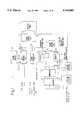
- FIG. 7is a schematic plan view showing the general constitution of the AC-type three-electrode plasma display panel (PDP) mentioned above, and FIG. 8 is a schematic sectional view of a discharge cell 10 of the plasma display panel shown in FIG. 7.
- PDPAC-type three-electrode plasma display panel
- the plasma display panelis constituted by two glass substrates 12 and 13.
- the first substrate 13includes first electrodes (X-electrodes) 14 that are disposed in parallel with one another and work as sustaining electrodes, and second electrodes (Y-electrodes) 15 which are covered with a dielectric layer 18.
- a film 21composed of MgO (magnesium oxide) or the like which serves as a protective film.
- electrodes 16that work as third electrodes or address electrodes and intersect the sustaining electrodes 14 and 15 at right angles.
- a fluorescent substance 19having any one of red, green and blue light-emitting properties on the same surface as the surface of the second substrate 12 on which the address electrode is disposed within a discharge space 20 defined by wall portions 17.
- each of the discharge cells 10 in the plasma displayis partitioned by walls (barrier walls).
- the first electrodes (X-electrodes) 14 and the second electrodes (Y-electrodes) 15are arranged in parallel with each other to form pairs, the second electrodes (Y-electrodes) 15 being separately driven whereas the first electrodes (X-electrodes) 14 constituting a common electrode so as to be driven by a single driver.
- FIG. 9is a schematic block diagram showing peripheral circuits for driving the plasma display shown in FIGS. 7 and 8, wherein a display panel 30 having, for example, the structure as described above displays a predetermined picture being controlled by a panel driver circuit 31 which includes an address driver means for driving the address electrodes, and a driver means for separately driving the X- and Y-electrodes.
- a dot-clock signalwhich is an address data for driving the address electrodes and display data are input to a data control circuit 33.
- the above signalsare input to the panel driver circuit 31 to drive a predetermined address electrode and to apply a predetermined display data to, for example, a predetermined cell portion of a selected Y-electrode.
- a VSYNC signalwhich is a vertical synchronizing signal output for every frame
- a signal HSYNCwhich is a horizontal synchronizing signal output for every sub-frame
- the scan control circuit 34changes the frequency of the discharge-sustaining voltage pulses applied to the X- and Y-electrodes in order to sustain electric discharges in the above-mentioned selected cell portion and to control the brightness of the display screen. More specifically, a current detecting means 37 detects the current consumed by the display panel when a display voltage Vs is applied to the display panel, the value of which is converted into 8-bit digital data through an analog/digital converter 36, and then the 8-bit data is converted into, for example, a 7-bit control code through a microcontroller (MPU) 35, and is input to a sustain counter 45 provided in the scan control circuit 34, in order to suitably change the frequency of the discharge-sustaining pulses and to adjust the brightness.
- MPUmicrocontroller
- the electrodes arranged on the inner surfaces of the two opposing glass substrates 12 and 13do not include the X-electrodes shown in FIG. 7, but include anodes (anode electrodes) Al to AM that correspond to address electrodes and cathodes (cathode electrodes) Kl to KN that correspond to Y-electrodes of FIG. 7 and that intersect the anodes (anode electrodes) at right angles.
- the panel 10is constituted by disposing two glass substrates, i.e., the front glass substrate 12 and the rear glass substrate 13, in an opposing manner as in FIG. 8.
- a mixture gascomprising, for example, helium He and xenon Xe is sealed between the two glass substrates, and a predetermined discharge space is formed by suitable wall portions 17.
- a suitable voltageis applied across the cathode KN and the anode AM whereby electric discharge takes place in a space partitioned by the wall portions 17, i.e., between the cathode KN and the anode AM in the display cell, and the fluorescent substance is excited by ultraviolet rays produced at this moment to thereby emit light.
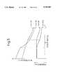
- the brightness of the display panel 30 in the plasma display (DC-PDP)abruptly increases with an increase in the discharge voltage pulse. That is, when attention is given to a discharge spot unit 70 at a cell portion 10 constituted at an intersecting point of the anode electrode AM and the cathode electrode KN, the discharge area of the discharge spot 70 abruptly increases with an increase in the discharge voltage pulse as represented by a change from FIG. 10(A) to FIG. 1O(B), and the dot brightness at the light-emitting portion increases.
- the discharge spot 20occurs only inside the discharge gap when the applied voltage is small, as shown in FIG. 11(A), but the area of the discharge spot 70 increases with an increase in the voltage as shown in FIG. 11(B), and brightness at the light-emitting portion increases.
- the high voltage Vs for display applied to the displayis input to the panel drive circuit 31 through the current detecting circuit 37, the detected current value is converted into 8-bit data through the 8-bit A/D converter 36 and is input to a calculation unit or MDU (constituted by a microcontroller, etc.) 35 which determines whether the detected current value is larger than a preset current converging value.
- MDUconstituted by a microcontroller, etc.
- a frequency conversion control signal for the discharge-sustaining pulsesis output in the form of a 7-bit code from the calculation means 35 to the scan control circuit 34.
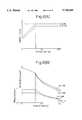
- FIGS. 12 and 13are graphs respectively showing the relationship between the current I s flowing into the display panel, and the brightness and frequency of discharge-sustaining pulses (sustaining pulses) using the display voltage Vs as a parameter when the display rate (%) is changed in the flat-display panel of the prior art.
- the current I sincreases with an increase in the display rate as shown in FIG. 12, and a difference develops depending upon the voltage Vs, as represented by curve a and curve b.
- the curve ashows a case when the voltage Vs is large
- the curve bshows a case when the voltage Vs is small.
- the brightnesstends to decrease as the display rate increases, and the degree of brightness becomes higher as the voltage Vs becomes higher, as represented by a curve e, and the brightness decreases as the voltage Vs becomes small, as represented by a curve d.
- the level of brightnesscan be changed depending upon the display rate by changing the frequency.
- the brightnesschanges as represented by curves d and e inclusive of dotted line curves in FIG. 13 and when the frequency is changed, the brightness can be changed as represented by solid line curves d' and e'.
- the level of brightnessdecreases with an increase in the display rate and there exists a large difference in the brightness depending upon a difference in the display voltage Vs.
- the frequency of the discharge-sustaining pulsesis lowered so that a current larger than a predetermined value will not flow, i.e., so that the current will not become larger than a predetermined value as represented by a solid curve c in FIG. 12.
- the current flowing into the display panelshould be decreased by lowering the frequency as represented by curves f and g in FIG. 13.
- the brightnessdecreases with a decrease in the frequency as a matter of course.
- the problemis how to attain the optimum display rate and brightness with the optimum current consumption by adjusting the above-mentioned factors.
- a maximum currentis set depending upon the specifications as described above. Therefore, the maximum current must be determined by taking the worst conditions into account.
- a setpoint voltagemust have a margin and, hence, must be determined with a maximum display voltage Vs as a reference.
- a limit currentis determined by the maximum value of the display voltage Vs and, hence, the brightness is determined accordingly.
- the brightnessdiffers to a considerable degree depending upon the difference in the setpoint voltage, i.e., on the display voltage Vs. Therefore, the brightness undergoes a change depending upon a change in the setpoint display voltage Vs, causing the quality of image to deteriorate.
- a display panelin which at least two electrode arrays having a plurality of electrodes forming cell portions that constitute pixels, and said cell portions have a function for emitting light in accordance with suitable display data and drive voltage pulses applied to said electrodes, characterized by the provision of a control means for controlling a current which increases with an increase in the turn-on display rate of said cell portions, a current detecting means for detecting the current flowing into said cell portions, and a current converging value setting means for arbitrarily setting a converting value of the current flowing into said cell portions.
- the flat-display panel according to the present inventionemploys the technical constitution that is described above. Basically, therefore, the invention is based on a technical idea in which attention is given to the electric power, i.e., the electric power is maintained constant and, under this condition, the current to be converged is increased when the voltage is low, i.e., when the display voltage Vs is low, making it possible to increase the brightness.
- the frequencyis changed by changing the current converging value depending upon the display voltage Vs, whereby the difference in the brightness due to a difference in the display voltage Vs is minimized in order to realize an image display maintaining stable brightness.
- the level of the current value to be convergedis set to be high whereby the frequency of drive voltage pulses is increased to increase the brightness. Accordingly, the level of brightness becomes high when the display voltage Vs is low and is brought close to the brightness level of when the display voltage Vs is high. Thus, a change in the brightness caused by a difference in the display voltage Vs is decreased.
- FIG. 1is a block diagram illustrating the constitution of a flat-display panel according to an embodiment of this invention.
- FIG. 2is a block diagram illustrating the constitution of a current detecting means employed in the flat-display panel according to the embodiment of this invention.
- FIG. 3is a block diagram illustrating the constitution of a voltage detecting means employed in the flat-display panel according to the embodiment of this invention.
- FIG. 4is a graph showing the relationship between the display rate and the current when the display operation is carried out by the flat-display panel of this invention.
- FIG. 5is a graph showing the relationship between the display rate, the brightness and the frequency when the display operation is carried out by the flat-display panel of this invention.
- FIG. 6(A)is a graph showing the relationship between the display rate and the current when another display operation is carried out by the flat-display panel of this invention
- FIG. 6(B)is a graph showing the relationship between the display rate, the brightness and the frequency.
- FIG. 7is a plan view illustrating the constitution of a display means employed in a prior art flat-display panel which is an AC-type plasma display.
- FIG. 8is a sectional view illustrating the constitution of a cell portion in the prior art flat-display panel which is the AC-type plasma display.
- FIG. 9is a block diagram illustrating the constitution of a drive circuit in the prior art flat-display panel.
- FIGS. 1O(A) and 10(B)are diagrams showing the state of electric discharge in a cell portion in the prior art flat-display panel.
- FIGS. 11(A) and 11(B)are diagrams showing the state of electric discharge in a cell portion in the prior art flat-display panel.
- FIG. 12is a graph showing the relationship between the display rate and the current during the display driving of a prior art flat-display panel.
- FIG. 13is a graph showing the relationship between the display rate, the brightness and the frequency during the display driving of the prior art flat-display panel.
- FIG. 14is a diagram showing an example of frequency control data used in the flat-display panel according to this invention.
- FIG. 15is a block diagram illustrating the constitution of a scan controller circuit used in the flat-display panel according to the embodiment of this invention.
- FIG. 16is a plan view illustrating the constitution of a display means employed in a prior art flat-display panel which is a DC-type plasma display.
- FIG. 17is a sectional view illustrating the constitution of a cell portion in the prior art flat-display panel which is the DC-type plasma display.
- FIG. 18is a diagram illustrating a large planar display system using the flat-displays panel according to this invention.
- FIG. 19is a diagram illustrating a large cylindrical display system using the flat-displays panel according to this invention.
- the basic constitution of the flat-display panel of the present inventionis concerned with a flat-display panel in which at least two electrode arrays, each having a plurality of electrodes, define cell portions that constitute pixels, and said cell portions have a function of emitting light in accordance with suitable display data and drive voltage pulses applied to said electrodes, characterized by the provision of a control means for controlling a current which increases with an increase in the turn-on display rate of said cell portions, a current detecting means for detecting the current flowing into said cell portions, and a current converging value setting means for arbitrarily setting a converging value of the current flowing into said cell portions.
- the flat-display panelmay be a plasma display or an electroluminescence display.
- the drive voltage pulsemay be a discharge-sustaining voltage pulse and the cell portion should have a function for emitting light upon discharge, in accordance with suitable display data and the discharge-sustaining voltage pulse applied to the electrodes.
- control means for controlling the currentis a turn-on frequency control means which controls said current based upon the frequency of said drive voltage pulses.
- FIG. 1is a block diagram illustrating a concrete constitution ofthe flat-display panel of the invention, i.e., illustrating a flat-display panel in which at least two substrates having electrodes arranged on the surfaces thereof are disposed adjacent to each other so that said electrodes face each other at right angles, a suitable fluorescent substance is inserted between the substrates, a plurality of right-angled intersecting portions constituted between said electrodes have display-means-forming cell portions that constitute pixels, and said cell portions have a function for emitting light upon discharge in accordance with suitable display data and discharge-sustaining pulses applied to saidelectrodes, characterized by the provision of a turn-on frequency control unit for controlling a current which increases with an increase in the turn-on display rate of said display means based upon the frequency of said discharge-sustaining pulses, a current detecting means for detecting the current flowing into said cell portions, and a current converging value setting means for arbitrarily setting a conver
- the flat-display panel according to the present inventionmay be a plasma display or an electroluminescence display.
- the electroluminescence displayone substrate, on both opposite surfaces of which corresponding pluralities of electrodes are arranged, may be used.
- the flat-display panel 30may be of anytype, provided the cell portions constituting the display panel 30 of the flat-display panel are so constituted that the operation for emitting light upon discharge can be controlled by changing the frequency of the discharge-sustaining pulses.
- FIG. 1The basic constitution of the flat-display panel system according to the present invention shown in FIG. 1 is nearly the same as that of the prior art flat-display panel shown in FIG. 9, and the same circuits and same means are denoted by the same reference numerals but their details are undepeated here.
- the characteristic constitution of the flat-display panel system 1 according to the present inventionis as shown in FIG. 1, wherein a voltage detector 39 for detecting the display voltage Vs is disposed in series with a current detector 37, and an output of the voltage detector 39 and an output of the current detector 37 are separately input to a selector 38 which outputs predetermined data to the 8-bit A/C converter 36in response to a suitable select command SL1, so that the 8-bit detected data is input to the microcontroller 35.
- a current converging value setting 41which stores data related to predetermined current converging values, is connected to the microcontroller 35.
- the current converging value setting unit 41Upon receiving a request signal from the microcontroller 35, the current converging value setting unit 41 readsthe current converging value data, corresponding to the data of display voltage Vs received by the microcontroller 35, and sends the data to the microcontroller 35.
- the microcontroller 35sets a predetermined current converging value, basedupon the control data, so that it can be used as a basis for the subsequentcalculation.
- the turn-on frequency control unit 40 in the flat-display panel system 1 in accordance with this inventionso controls the frequency of the discharge-sustaining pulses of the cell portions that the current, flowing into the cell portions of the display panel 30, is converged into the current converging value set by the current converging value setting panel 41.
- the calculation panel 35constituted by a microcontroller or the like, which is provided with a frequency setting unit 47 which changes the frequency of the discharge-sustaining pulses, which sustain the discharge,by alternatingly changing the polarity of the display voltage Vs applied tothe cell portions of the display panel 30, relying upon the input current data and in compliance with a predetermined calculation program.
- the data for controlling the discharge-sustaining pulsesare formed by the frequency setting unit 47 and are input to a sustain counter circuit 45 provided in the scan controller circuit 34.
- the above-mentioned control operationcan be executed relying basically upon the current data detected by the current detector 37. Furthermore, in order to realize the object of this invention more correctly and concretely, there may be further provided a voltage detector to detect the display voltage Vs, and conditions may be introduced so as to maintain the electric power constant by using both thecurrent value and the display voltage value Vs, and the current value and the voltage value many be changed in order to accomplish the production ofan image display which maintains a predetermined stable brightness while consuming a reduced amount of electrical power.
- the flat-display panel system according to the present inventionmay be further provided with a voltage detector 39 for detecting the turn-on display voltage applied to the display 30, and with an electric power calculator unit 46 in the MPU 35, constituted by a microcontroller or the like, in order to calculate the power (voltage x current) value from an output of the voltage detector 39 and an output of the current detector 37and in which the turn-on frequency control unit 40 may so control the frequency of the discharge-sustaining pulses that the power value is maintained constant.
- Constitutions of the current detector 37 and voltage detector 39 used in the flat-display panel system 1 in accordance with this inventionare not specifically limited, and any known detectors may be used.
- An example of the current detector 37is shown in FIG. 2 and an example of the voltage detector 39 is shown in FIG. 3.
- FIG. 2illustrates a concrete constitution of the current detector 37 used in the present invention.
- the current detector 37is provided in the circuit which connects the power source of the display voltage Vs to the panel drive circuit 31; a resistor R4 is inserted in the circuit, the emitters of bipolar transistors TR1 and TR2 are connected to respective, opposite ends of the resistor R4, and the bases of the transistors TR1 andTR2 are connected in common.
- the collector of the transistor TR2is grounded via resistor R3 and is further connected to the base of the transistor TR2.
- the collector of the transistor TR1is grounded via resistor R1 and is further connected to an end of a capacitor Cl via resistor R2, and the connection point, or node, thereof is connected to a comparator circuit 4 which will be described later.
- the current value detected by the current detector 37is input to a terminal A of the selector circuit 38 provided in the turn-on frequency control unit 40.
- FIG. 3illustrates the constitution of a display voltage Vs detecting circuit 39 that can be used in the present invention.
- the voltage detector 39is provided in the circuit that connects the power source of the display voltage Vs to the panel drive circuit 31.
- Resistor R5is connected to node N1 in the interconnecting circuit and in series at node N2 with resistor R6 and, further, resistor R6 is connected to ground.
- Resistor R7is connected to node N2 and in series at node N3 with capacitor C2 and capacitor C2 further is connected to ground.
- a voltage detected at node N3, at which the resistor R7 and the capacitor C2 are connected together,is input to aterminal B of the selector circuit 38 provided in the turn-on frequency control unit 40.
- the current and voltage according to this inventioncan be stored in a suitable memory 42 provided in the MPU 40, that is constituted by a microcontroller or the like, in the turn-on frequency control unit 40.
- the voltage valueis specific to the display unit 30 that is used and, once it is measured, then the same voltage is obtained hereinafter. Accordingly, if a voltage measured first is stored in the memory means 42, the voltage data can be read out from the memory means 42and can be used at any time.
- the memorymay store the data in such a manner that a first control data is used when a high voltage is detected, a second control data is used when an intermediate voltage is detected and a third control data is used when a low voltage is detected. Then, suitable control data can be read out from the memory depending upon a voltage that is subsequently detected.
- the current converging value setting unit 41 used in the present inventionstores the control data related to an optimum current converging value that corresponds to a predetermined valvein the form of, for example, a look-up table, and feeds predetermined control data, corresponding to the detected voltage, to the turn-on frequency control unit 40.
- the turn-on frequency control unit 40is provided with a frequency setting unit 47 for attaining a proper brightness by taking into consideration thecurrent and voltage values that are detected and the current converging data fed from the current converging value setting unit 41 under the condition where the electric power output from the electric power calculator 46 remains constant.
- the frequency setting unit 47outputs a signal for controlling the scan control circuit 34 so as to accomplish a predetermined frequency of the discharge-sustaining pulses.
- a look-up tableis prepared in which control data related to the frequency for controlling the scan control circuit 34 are 7-bit coded. A predetermined control data is selected from the look-up table and is fed to the scan control circuit 34.
- the look-up tableis constituted by, for example, 128 steps of different frequency control data.
- FIG. 14An example of the look-up table is shown in FIG. 14.
- the scan control circuit 34repeats the operation in which a head address of the minimum data unit of the waveform program is latched and the head address previously latched at the final address of the minimum data unit is loadedinto the address counter, and the program is shifted to the next minimum data unit.
- an input signal Vccauses the blocks to be reset, and the address counter 52 starts operating.
- the head address, at which the counted value enters into the scan cycle,islatched by the address latch 50 in response to a latch clock from an address latch counter control ROM 57, and the latched address data is loaded into the address counter 52 in response to a load signal from the address latch counter control ROM 57 at the time of a last address in the scan cycle.
- the address counter 52leaves the scan cycle and enters into the sustain cycle. Even in the sustain cycle, the same operation as the scan cycle is carried out at places of the head address and the last address.
- the sustain counter 57counts the number of sustaining pulses and, when thecounted value coincides with the output of the comparator 58, the load signal is inhibited and the sustain counter leaves the scan cycle.
- the output of the comparator 58is determined by the outputstate of a field counter 60 and by the output state of a brightness switch 61.
- the address counteris reset by a reset signal (RESET) from the address latch counter control ROM57 and starts operating from the write cycle.
- RESETreset signal
- the field counter 60counts up every time all of the cycles are finished.
- the frequency of the discharge-sustaining pulsesis changed by inputting a control signal to the above-mentioned brightness switch SW 61 from the frequency setting means 47 provided in the calculation means 35 which is constituted by a microcontroller or the likein accordance with the present invention.
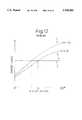
- FIGS. 4 and 5are graphs showing the effects when the image display scanning is executed by using the aforementioned flat-display panel of thepresent invention.
- the current value to be convergedis changed from the conventional fixed system into a variable system, based upon the technical idea of maintaining the electric power constant. Therefore, the state of optimum brightness is easily maintained despite a change in the display voltage Vs.
- the difference in the brightness level due to a difference in the display voltage Vsdecreases in a region of high display rate, making it possible to display an image stably and with high quality.
- the brightness levelin a state where the display voltage Vs is low, can be brought close to the brightness level in a state where the display voltage Vs is high since theelectric power is maintained to be not larger than a predetermined value.
- FIGS. 6(A) and 6(B)are graphs showing effects obtained by the flat-displaypanel system according to another embodiment of this invention, wherein theoperation as a whole is carried out at higher frequencies by eliminating the difference in the brightness level caused by a difference in the display voltage Vs even when the turn-on frequency is low, and setting thedisplay voltage Vs at a minimum value which does not cause any problem in the display, so that uniform and stable brightness is obtained over the whole range of display rates.
- the frequencyis set to be high in order to eliminate a difference in the brightness between when the display voltage Vs is highand when the display voltage Vs is low. It will therefore be recognized that the current is increased, and the control operation is started with asmall (i.e., low) display rate in which the current is maintained constant,by the microcontroller 35.
- the frequencyis adjusted in a region where the display rate is low in order to eliminate the difference in the brightness caused by a change in the display voltage Vs.
- the flat-display panel according to this inventionminimizes the difference in the brightness level caused by a difference inthe display voltage Vs. Therefore, even when a large multiple display is constituted by arranging a plurality of the flat-displays panel in the form of a matrix, little difference in the brightness is exhibited by the flat-displays panel and the thus constituted large display appears even.
- a plurality of the displaysmay be arranged in a cylindrical formto constitute a large public display.
- FIG. 18shows the constitution of a large planar display system in which a plurality of displays according to the present invention are arranged in the form of a matrix on a predetermined panel unit 181. In this case, sixteen of the flat-displays panel 182 of the present invention are used.
- FIG. 19shows a large cylindrical display constituted by arranging thirty-two flat-display panels 192 of this invention in the form of a matrix on the surface of a suitable cylindrical member 191.
- the method of driving the flat-display panel according to this inventionis already obvious from the foregoing description, a basic technical constitution therefor will be briefly described below.
- the first display driving method of controlling the flat-display panela current flowing into the display panel 30 is detected in the above-constituted flat-display panel system and the current converging value is set to a given value in response to the detected current so that the current is controlled to acquire a predetermined value.
- the second display driving method of controlling the flat-display panelin controlling the turn-on display rate, the frequency of the discharge-sustaining voltage pulses is controlled in a manner that the current flowing into the display means is converged into a value set by the preset current converging value.
- the voltage for turning-on the display applied to the display meansis detected in the flat-display panel and, at the same time,the power (voltage ⁇ current) value is calculated from an output of thevoltage detecting means and an output of the current detecting means, and the frequency of the discharge-sustaining voltage pulses is so controlled that the power value is maintained constant.
- the frequency of the discharge-sustaining voltage pulsesis set to a predetermined value in response to the detected displayvoltage in the above-mentioned methods of driving the flat-display panel.
- control data corresponding to the detected voltage valueis stored and, when the voltage is again detected, the control data corresponding to the detected voltage is compared with the stored data to control the display in the above-mentioned methods of driving the flat-display panel.
- the current converging valueis changed depending upon the display voltage Vs thereby to change the frequency, and the difference in the brightness caused by a difference in the display voltage Vs is minimized, making it possible to realize a display maintaining a stabilized brightness.
- the current value to be convergedis set to a high level in order to increase the frequency of the discharge-sustaining pulses and hence to increase the brightness. Therefore, the brightness level when the display voltage Vs is low is heightened to become close to the brightness level when the display voltage Vs is high, making it possible to decrease a change in the brightness caused by a difference in the display voltage Vs.
- the flat-display panelis capable of displaying an image with a stabilized brightness while suppressing a change in the brightness,regardless of a change in the display rate or a change in the display voltage Vs.
Landscapes
- Engineering & Computer Science (AREA)
- Physics & Mathematics (AREA)
- Power Engineering (AREA)
- Plasma & Fusion (AREA)
- Computer Hardware Design (AREA)
- General Physics & Mathematics (AREA)
- Theoretical Computer Science (AREA)
- Control Of Indicators Other Than Cathode Ray Tubes (AREA)
Abstract
Description
Claims (20)
Priority Applications (1)
| Application Number | Priority Date | Filing Date | Title |
|---|---|---|---|
| US08/412,137US5745085A (en) | 1993-12-06 | 1995-03-28 | Display panel and driving method for display panel |
Applications Claiming Priority (5)
| Application Number | Priority Date | Filing Date | Title |
|---|---|---|---|
| JP5-305415 | 1993-12-06 | ||
| JP30541593 | 1993-12-06 | ||
| US18890994A | 1994-01-31 | 1994-01-31 | |
| US38437195A | 1995-02-02 | 1995-02-02 | |
| US08/412,137US5745085A (en) | 1993-12-06 | 1995-03-28 | Display panel and driving method for display panel |
Related Parent Applications (1)
| Application Number | Title | Priority Date | Filing Date |
|---|---|---|---|
| US38437195AContinuation-In-Part | 1993-12-06 | 1995-02-02 |
Publications (1)
| Publication Number | Publication Date |
|---|---|
| US5745085Atrue US5745085A (en) | 1998-04-28 |
Family
ID=27338751
Family Applications (1)
| Application Number | Title | Priority Date | Filing Date |
|---|---|---|---|
| US08/412,137Expired - LifetimeUS5745085A (en) | 1993-12-06 | 1995-03-28 | Display panel and driving method for display panel |
Country Status (1)
| Country | Link |
|---|---|
| US (1) | US5745085A (en) |
Cited By (39)
| Publication number | Priority date | Publication date | Assignee | Title |
|---|---|---|---|---|
| US5889502A (en)* | 1996-01-12 | 1999-03-30 | Sony Corporation | Discharge voltage control for plasma addressed display device |
| WO2000017845A1 (en)* | 1998-09-18 | 2000-03-30 | Matsushita Electric Industrial Co., Ltd. | Colour display apparatus |
| EP0991051A1 (en)* | 1998-09-30 | 2000-04-05 | Mitsubishi Denki Kabushiki Kaisha | Control circuit for display panel |
| US6069597A (en)* | 1997-08-29 | 2000-05-30 | Candescent Technologies Corporation | Circuit and method for controlling the brightness of an FED device |
| US6160541A (en)* | 1997-01-21 | 2000-12-12 | Lear Automotive Dearborn Inc. | Power consumption control for a visual screen display by utilizing a total number of pixels to be energized in the image to determine an order of pixel energization in a manner that conserves power |
| US6204610B1 (en)* | 1999-03-18 | 2001-03-20 | Sanyo Electric Co., Ltd. | Electroluminescence display device |
| US6278421B1 (en)* | 1996-11-06 | 2001-08-21 | Fujitsu Limited | Method and apparatus for controlling power consumption of display unit, display system equipped with the same, and storage medium with program stored therein for implementing the same |
| US20010033252A1 (en)* | 2000-04-18 | 2001-10-25 | Shunpei Yamazaki | Display device |
| US20020044145A1 (en)* | 1993-11-19 | 2002-04-18 | Fujitsu Limited Of Kawasaki | Flat display panel having internal lower supply circuit for reducing power consumption |
| US6400346B2 (en)* | 1997-12-10 | 2002-06-04 | Matsushita Electric Industrial Co., Ltd. | Display apparatus capable of adjusting subfield number according to brightness |
| US6424326B2 (en)* | 2000-01-11 | 2002-07-23 | Semiconductor Energy Laboratory Co., Ltd. | Semiconductor display device having a display portion and a sensor portion |
| US6426732B1 (en)* | 1997-05-30 | 2002-07-30 | Nec Corporation | Method of energizing plasma display panel |
| US6437848B1 (en)* | 1999-08-02 | 2002-08-20 | Minolta Co., Ltd. | Liquid crystal light modulating element |
| US6445368B1 (en)* | 1998-03-27 | 2002-09-03 | Sony Corporation | Display device having intergrated operating means |
| US20020149548A1 (en)* | 2001-04-13 | 2002-10-17 | Hitachi, Ltd. | Plasma display panel driving method, driving circuit and image displaying device |
| US20020167381A1 (en)* | 2001-05-08 | 2002-11-14 | Pioneer Corporation | Display panel drive apparatus |
| US6522314B1 (en)* | 1993-11-19 | 2003-02-18 | Fujitsu Limited | Flat display panel having internal power supply circuit for reducing power consumption |
| US6570559B1 (en)* | 1997-05-15 | 2003-05-27 | Sony Corporation | Information display apparatus, and display state detection method, display state adjustment method and maintenance management method therefor |
| US20030098822A1 (en)* | 2001-11-24 | 2003-05-29 | Park Chung Hoo | Apparatus and method for driving plasma display panel |
| US20030122813A1 (en)* | 2001-12-28 | 2003-07-03 | Pioneer Corporation | Panel display driving device and driving method |
| US20030132716A1 (en)* | 2000-06-13 | 2003-07-17 | Semiconductor Energy Laboratory Co., Ltd, A Japan Corporation | Display device |
| US6701263B2 (en)* | 2000-09-01 | 2004-03-02 | Lg Electronics Inc. | Method and apparatus for displaying electric power elements for video display appliance |
| US20040085265A1 (en)* | 2002-10-31 | 2004-05-06 | Samsung Electronics Co., Ltd. | Low power consumption PDP with high speed response |
| EP1437705A1 (en)* | 2003-01-10 | 2004-07-14 | Deutsche Thomson-Brandt Gmbh | Method for optimizing brightness in a display device and apparatus for implementing the method |
| US6822644B1 (en)* | 1999-06-30 | 2004-11-23 | Fujitsu Limited | Method and circuit for driving capacitive load |
| US20050007027A1 (en)* | 2003-07-07 | 2005-01-13 | Fryer Christopher James Newton | Control of electroluminescent displays |
| US20050024357A1 (en)* | 2000-08-29 | 2005-02-03 | Atsushi Kota | Driving circuit of display and display device |
| US6914595B1 (en)* | 1999-09-29 | 2005-07-05 | Sanyo Electric Co., Ltd. | Digitizing apparatus |
| US20060027822A1 (en)* | 2004-08-05 | 2006-02-09 | Jin-Hyun Choi | Light emitting display and driving method thereof |
| US20070139406A1 (en)* | 2005-12-05 | 2007-06-21 | Sony Corporation | Self light emission display device, power consumption detecting device, and program |
| EP1437706A3 (en)* | 2003-01-10 | 2007-10-10 | Thomson Licensing | Method for optimizing brightness in a display device and apparatus for implementing the method |
| US20080079664A1 (en)* | 2004-07-21 | 2008-04-03 | Satoshi Ikeda | Plasma Display Device |
| CN100442346C (en)* | 2003-06-11 | 2008-12-10 | 精工爱普生株式会社 | semiconductor integrated circuit |
| EP1594114A3 (en)* | 2004-05-07 | 2009-09-16 | Pioneer Corporation | Display device |
| US20100013747A1 (en)* | 2008-07-16 | 2010-01-21 | Semiconductor Energy Laboratory Co., Ltd. | Light-Emitting Device and Driving Method Thereof |
| US8144146B2 (en) | 2004-05-21 | 2012-03-27 | Semiconductor Energy Laboratory Co., Ltd. | Display device and electronic device |
| US8194006B2 (en) | 2004-08-23 | 2012-06-05 | Semiconductor Energy Laboratory Co., Ltd. | Display device, driving method of the same, and electronic device comprising monitoring elements |
| US8960593B2 (en) | 2011-05-03 | 2015-02-24 | Raytheon Company | Horizon scanning system for a rotary wing aircraft including sensors housed within a tubercle on a rotor blade |
| US10363409B2 (en) | 2011-09-01 | 2019-07-30 | Zoll Medical Corporation | Medical equipment electrodes |
Citations (12)
| Publication number | Priority date | Publication date | Assignee | Title |
|---|---|---|---|---|
| US4032818A (en)* | 1975-11-10 | 1977-06-28 | Burroughs Corporation | Uniform current level control for display panels |
| US4414544A (en)* | 1981-06-12 | 1983-11-08 | Interstate Electronics Corp. | Constant data rate brightness control for an AC plasma panel |
| US4692665A (en)* | 1985-07-05 | 1987-09-08 | Nec Corporation | Driving method for driving plasma display with improved power consumption and driving device for performing the same method |
| JPH01193797A (en)* | 1988-01-28 | 1989-08-03 | Deikushii Kk | Spontaneous light emission type display device |
| US4859910A (en)* | 1986-07-22 | 1989-08-22 | Nec Corporation | Plasma display apparatus |
| JPH03182792A (en)* | 1989-12-12 | 1991-08-08 | Fujitsu Ltd | Plasma display panel drive device |
| US5068740A (en)* | 1988-07-21 | 1991-11-26 | Magnascreen Corporation | Modular flat-screen television displays and modules and circuit drives therefor |
| JPH03269482A (en)* | 1990-03-19 | 1991-12-02 | Fujitsu Ltd | Display device |
| JPH04128874A (en)* | 1990-09-20 | 1992-04-30 | Fujitsu Ltd | Drive circuit for light emitting display device |
| US5126632A (en)* | 1988-05-10 | 1992-06-30 | Parker William P | Luminous panel display device |
| JPH05181430A (en)* | 1991-06-17 | 1993-07-23 | Toshiba Corp | Device and method for power source control for computer system |
| US5325107A (en)* | 1988-11-30 | 1994-06-28 | Sharp Kabushiki Kaisha | Method and apparatus for driving a display device |
- 1995
- 1995-03-28USUS08/412,137patent/US5745085A/ennot_activeExpired - Lifetime
Patent Citations (12)
| Publication number | Priority date | Publication date | Assignee | Title |
|---|---|---|---|---|
| US4032818A (en)* | 1975-11-10 | 1977-06-28 | Burroughs Corporation | Uniform current level control for display panels |
| US4414544A (en)* | 1981-06-12 | 1983-11-08 | Interstate Electronics Corp. | Constant data rate brightness control for an AC plasma panel |
| US4692665A (en)* | 1985-07-05 | 1987-09-08 | Nec Corporation | Driving method for driving plasma display with improved power consumption and driving device for performing the same method |
| US4859910A (en)* | 1986-07-22 | 1989-08-22 | Nec Corporation | Plasma display apparatus |
| JPH01193797A (en)* | 1988-01-28 | 1989-08-03 | Deikushii Kk | Spontaneous light emission type display device |
| US5126632A (en)* | 1988-05-10 | 1992-06-30 | Parker William P | Luminous panel display device |
| US5068740A (en)* | 1988-07-21 | 1991-11-26 | Magnascreen Corporation | Modular flat-screen television displays and modules and circuit drives therefor |
| US5325107A (en)* | 1988-11-30 | 1994-06-28 | Sharp Kabushiki Kaisha | Method and apparatus for driving a display device |
| JPH03182792A (en)* | 1989-12-12 | 1991-08-08 | Fujitsu Ltd | Plasma display panel drive device |
| JPH03269482A (en)* | 1990-03-19 | 1991-12-02 | Fujitsu Ltd | Display device |
| JPH04128874A (en)* | 1990-09-20 | 1992-04-30 | Fujitsu Ltd | Drive circuit for light emitting display device |
| JPH05181430A (en)* | 1991-06-17 | 1993-07-23 | Toshiba Corp | Device and method for power source control for computer system |
Cited By (84)
| Publication number | Priority date | Publication date | Assignee | Title |
|---|---|---|---|---|
| US20090303221A1 (en)* | 1993-11-19 | 2009-12-10 | Hitachi Plasma Patent Licensin Co., Ltd. | Flat display panel having internal power supply circuit for reducing power consumption |
| US6522314B1 (en)* | 1993-11-19 | 2003-02-18 | Fujitsu Limited | Flat display panel having internal power supply circuit for reducing power consumption |
| US7592976B2 (en) | 1993-11-19 | 2009-09-22 | Hitachi Plasma Patent Licensing Co., Ltd. | Flat display panel having internal power supply circuit for reducing power consumption |
| US20020044145A1 (en)* | 1993-11-19 | 2002-04-18 | Fujitsu Limited Of Kawasaki | Flat display panel having internal lower supply circuit for reducing power consumption |
| US7068264B2 (en) | 1993-11-19 | 2006-06-27 | Hitachi, Ltd. | Flat display panel having internal power supply circuit for reducing power consumption |
| US20060176248A1 (en)* | 1993-11-19 | 2006-08-10 | Hitachi, Ltd. | Flat display panel having internal lower supply circuit for reducing power consumption |
| US5889502A (en)* | 1996-01-12 | 1999-03-30 | Sony Corporation | Discharge voltage control for plasma addressed display device |
| US6278421B1 (en)* | 1996-11-06 | 2001-08-21 | Fujitsu Limited | Method and apparatus for controlling power consumption of display unit, display system equipped with the same, and storage medium with program stored therein for implementing the same |
| US6160541A (en)* | 1997-01-21 | 2000-12-12 | Lear Automotive Dearborn Inc. | Power consumption control for a visual screen display by utilizing a total number of pixels to be energized in the image to determine an order of pixel energization in a manner that conserves power |
| US6570559B1 (en)* | 1997-05-15 | 2003-05-27 | Sony Corporation | Information display apparatus, and display state detection method, display state adjustment method and maintenance management method therefor |
| US6426732B1 (en)* | 1997-05-30 | 2002-07-30 | Nec Corporation | Method of energizing plasma display panel |
| US6069597A (en)* | 1997-08-29 | 2000-05-30 | Candescent Technologies Corporation | Circuit and method for controlling the brightness of an FED device |
| US6400346B2 (en)* | 1997-12-10 | 2002-06-04 | Matsushita Electric Industrial Co., Ltd. | Display apparatus capable of adjusting subfield number according to brightness |
| US6445368B1 (en)* | 1998-03-27 | 2002-09-03 | Sony Corporation | Display device having intergrated operating means |
| US6380943B1 (en) | 1998-09-18 | 2002-04-30 | Matsushita Electric Industrial Co., Ltd. | Color display apparatus |
| WO2000017845A1 (en)* | 1998-09-18 | 2000-03-30 | Matsushita Electric Industrial Co., Ltd. | Colour display apparatus |
| US6313814B1 (en) | 1998-09-30 | 2001-11-06 | Mitsubishi Denki Kabushiki Kaisha | Display control circuit for display panel |
| EP0991051A1 (en)* | 1998-09-30 | 2000-04-05 | Mitsubishi Denki Kabushiki Kaisha | Control circuit for display panel |
| CN1110784C (en)* | 1998-09-30 | 2003-06-04 | 三菱电机株式会社 | Display control circuit for display panel |
| US6204610B1 (en)* | 1999-03-18 | 2001-03-20 | Sanyo Electric Co., Ltd. | Electroluminescence display device |
| US6822644B1 (en)* | 1999-06-30 | 2004-11-23 | Fujitsu Limited | Method and circuit for driving capacitive load |
| US6437848B1 (en)* | 1999-08-02 | 2002-08-20 | Minolta Co., Ltd. | Liquid crystal light modulating element |
| US6914595B1 (en)* | 1999-09-29 | 2005-07-05 | Sanyo Electric Co., Ltd. | Digitizing apparatus |
| US7629610B2 (en) | 2000-01-11 | 2009-12-08 | Semiconductor Energy Laboratory Co., Ltd. | Semiconductor display device |
| US20050056841A1 (en)* | 2000-01-11 | 2005-03-17 | Semiconductor Energy Laboratory Co., Ltd., A Japan Corporation | Semiconductor display device |
| US7173279B2 (en) | 2000-01-11 | 2007-02-06 | Semiconductor Energy Laboratory Co., Ltd. | Semiconductor display device |
| US20070114532A1 (en)* | 2000-01-11 | 2007-05-24 | Semiconductor Energy Laboratory Co., Ltd. | Semiconductor display device |
| US7397064B2 (en) | 2000-01-11 | 2008-07-08 | Semiconductor Energy Laboratory Co., Ltd. | Semiconductor display device |
| US20080272374A1 (en)* | 2000-01-11 | 2008-11-06 | Semiconductor Energy Laboratory Co., Ltd. | Semiconductor display device |
| US20020180672A1 (en)* | 2000-01-11 | 2002-12-05 | Semiconductor Energy Laboratory Co., Ltd., A Japan Corporation | Semiconductor display device |
| US6828951B2 (en) | 2000-01-11 | 2004-12-07 | Semiconductor Energy Laboratory Co., Ltd. | Semiconductor display device |
| US6424326B2 (en)* | 2000-01-11 | 2002-07-23 | Semiconductor Energy Laboratory Co., Ltd. | Semiconductor display device having a display portion and a sensor portion |
| US20050017964A1 (en)* | 2000-04-18 | 2005-01-27 | Semiconductor Energy Laboratory Co., Ltd., A Japan Corporation | Display device |
| US7623099B2 (en) | 2000-04-18 | 2009-11-24 | Semiconductor Energy Laboratory Co., Ltd. | Display device |
| US7221338B2 (en) | 2000-04-18 | 2007-05-22 | Semiconductor Energy Laboratory Co., Ltd. | Display device |
| US20010033252A1 (en)* | 2000-04-18 | 2001-10-25 | Shunpei Yamazaki | Display device |
| US20050012731A1 (en)* | 2000-04-18 | 2005-01-20 | Semiconductor Energy Laboratory Co., Ltd., A Japan Corporation | Display device |
| US20110140997A1 (en)* | 2000-04-18 | 2011-06-16 | Semiconductor Energy Laboratory Co., Ltd. | Display device |
| US7623100B2 (en) | 2000-04-18 | 2009-11-24 | Semiconductor Energy Laboratory Co., Ltd. | Display device |
| US20050017963A1 (en)* | 2000-04-18 | 2005-01-27 | Semiconductor Energy Laboratory Co., Ltd., A Japan Corporation | Display device |
| US7990348B2 (en) | 2000-04-18 | 2011-08-02 | Semiconductor Energy Laboratory Co., Ltd. | Display device |
| US7623098B2 (en) | 2000-04-18 | 2009-11-24 | Semiconductor Energy Laboratory Co., Ltd. | Display device |
| US8194008B2 (en) | 2000-04-18 | 2012-06-05 | Semiconductor Energy Laboratory Co., Ltd. | Display device |
| US8400379B2 (en) | 2000-04-18 | 2013-03-19 | Semiconductor Energy Laboratory Co., Ltd. | Display device |
| US8638278B2 (en) | 2000-04-18 | 2014-01-28 | Semiconductor Energy Laboratory Co., Ltd. | Display device |
| US9196663B2 (en) | 2000-04-18 | 2015-11-24 | Semiconductor Energy Laboratory Co., Ltd. | Display device |
| US7298347B2 (en) | 2000-06-13 | 2007-11-20 | Semiconductor Energy Laboratory Co., Ltd. | Display device |
| US20030132716A1 (en)* | 2000-06-13 | 2003-07-17 | Semiconductor Energy Laboratory Co., Ltd, A Japan Corporation | Display device |
| US7239307B2 (en)* | 2000-08-29 | 2007-07-03 | Samsung Sdi Co., Ltd. | Driving circuit of display and display device |
| US20050024357A1 (en)* | 2000-08-29 | 2005-02-03 | Atsushi Kota | Driving circuit of display and display device |
| US6701263B2 (en)* | 2000-09-01 | 2004-03-02 | Lg Electronics Inc. | Method and apparatus for displaying electric power elements for video display appliance |
| US6947015B2 (en)* | 2001-04-13 | 2005-09-20 | Hitachi, Ltd. | Plasma display panel driving method, driving circuit and image displaying device |
| US20020149548A1 (en)* | 2001-04-13 | 2002-10-17 | Hitachi, Ltd. | Plasma display panel driving method, driving circuit and image displaying device |
| US7133006B2 (en)* | 2001-05-08 | 2006-11-07 | Pioneer Corporation | Display panel drive apparatus |
| US20020167381A1 (en)* | 2001-05-08 | 2002-11-14 | Pioneer Corporation | Display panel drive apparatus |
| US7170472B2 (en)* | 2001-11-24 | 2007-01-30 | Lg Electronics Inc. | Apparatus and method for driving plasma display panel |
| US20030098822A1 (en)* | 2001-11-24 | 2003-05-29 | Park Chung Hoo | Apparatus and method for driving plasma display panel |
| US7274363B2 (en)* | 2001-12-28 | 2007-09-25 | Pioneer Corporation | Panel display driving device and driving method |
| US20030122813A1 (en)* | 2001-12-28 | 2003-07-03 | Pioneer Corporation | Panel display driving device and driving method |
| US20040085265A1 (en)* | 2002-10-31 | 2004-05-06 | Samsung Electronics Co., Ltd. | Low power consumption PDP with high speed response |
| EP1437706A3 (en)* | 2003-01-10 | 2007-10-10 | Thomson Licensing | Method for optimizing brightness in a display device and apparatus for implementing the method |
| EP1437705A1 (en)* | 2003-01-10 | 2004-07-14 | Deutsche Thomson-Brandt Gmbh | Method for optimizing brightness in a display device and apparatus for implementing the method |
| US7173580B2 (en) | 2003-01-10 | 2007-02-06 | Thomson Licensing | Method for optimizing brightness in a display device and apparatus for implementing the method |
| US20040164933A1 (en)* | 2003-01-10 | 2004-08-26 | Sebastien Weitbruch | Method for optimizing brightness in a display device and apparatus for implementing the method |
| CN100442346C (en)* | 2003-06-11 | 2008-12-10 | 精工爱普生株式会社 | semiconductor integrated circuit |
| US7075240B2 (en)* | 2003-07-07 | 2006-07-11 | Pelikon Limited | Control of electroluminescent displays |
| US20050007027A1 (en)* | 2003-07-07 | 2005-01-13 | Fryer Christopher James Newton | Control of electroluminescent displays |
| EP1594114A3 (en)* | 2004-05-07 | 2009-09-16 | Pioneer Corporation | Display device |
| US8144146B2 (en) | 2004-05-21 | 2012-03-27 | Semiconductor Energy Laboratory Co., Ltd. | Display device and electronic device |
| US20080079664A1 (en)* | 2004-07-21 | 2008-04-03 | Satoshi Ikeda | Plasma Display Device |
| US7710356B2 (en) | 2004-07-21 | 2010-05-04 | Panasonic Corporation | Plasma display device |
| US7808458B2 (en)* | 2004-08-05 | 2010-10-05 | Samsung Mobile Display Co., Ltd. | Light emitting display and driving method thereof |
| US20060027822A1 (en)* | 2004-08-05 | 2006-02-09 | Jin-Hyun Choi | Light emitting display and driving method thereof |
| US8194006B2 (en) | 2004-08-23 | 2012-06-05 | Semiconductor Energy Laboratory Co., Ltd. | Display device, driving method of the same, and electronic device comprising monitoring elements |
| US8576147B2 (en) | 2004-08-23 | 2013-11-05 | Semiconductor Energy Laboratory Co., Ltd. | Display device and electronic device |
| US8902132B2 (en)* | 2005-12-05 | 2014-12-02 | Sony Corporation | Self light emission display device, power consumption detecting device, and program |
| US20070139406A1 (en)* | 2005-12-05 | 2007-06-21 | Sony Corporation | Self light emission display device, power consumption detecting device, and program |
| US20100013747A1 (en)* | 2008-07-16 | 2010-01-21 | Semiconductor Energy Laboratory Co., Ltd. | Light-Emitting Device and Driving Method Thereof |
| US9076694B2 (en) | 2008-07-16 | 2015-07-07 | Semiconductor Energy Laboratory Co., Ltd. | Light-emitting device and driving method thereof |
| US8441418B2 (en) | 2008-07-16 | 2013-05-14 | Semiconductor Energy Laboratory Co., Ltd. | Light-emitting device and driving method thereof |
| US8960593B2 (en) | 2011-05-03 | 2015-02-24 | Raytheon Company | Horizon scanning system for a rotary wing aircraft including sensors housed within a tubercle on a rotor blade |
| US10363409B2 (en) | 2011-09-01 | 2019-07-30 | Zoll Medical Corporation | Medical equipment electrodes |
| US11224738B2 (en) | 2011-09-01 | 2022-01-18 | Zoll Medical Corporation | Medical equipment electrodes |
| US12214185B2 (en) | 2011-09-01 | 2025-02-04 | Zoll Medical Corporation | Medical equipment electrodes |
Similar Documents
| Publication | Publication Date | Title |
|---|---|---|
| US5745085A (en) | Display panel and driving method for display panel | |
| US6720940B2 (en) | Method and device for driving plasma display panel | |
| JP2000047634A (en) | Driving method of plasma display device | |
| EP1406238B1 (en) | Method and apparatus for driving plasma display panel | |
| EP1748407A1 (en) | Plasma display apparatus and driving method of the same | |
| US7663573B2 (en) | Plasma display panel and driving method thereof | |
| US6400347B1 (en) | Method for driving sustain lines in a plasma display panel | |
| JP3918134B2 (en) | Flat display device and driving method thereof | |
| US20030214464A1 (en) | Method for driving plasma display panel | |
| KR100798519B1 (en) | Plasma display device | |
| US7592974B2 (en) | Display device | |
| US6400342B2 (en) | Method of driving a plasma display panel before erase addressing | |
| US6876342B2 (en) | Plasma display apparatus and driving method thereof | |
| US20070120769A1 (en) | Plasma display apparatus and method of driving the same | |
| US20090009435A1 (en) | Method of Driving Plasma Display Panel and Plasma Display Unit | |
| KR100509756B1 (en) | Method Of Driving Plasma Display Panel Using High Frequency | |
| KR20070057372A (en) | Plasma display device and driving method thereof | |
| KR100520822B1 (en) | Apparatus for Driving Plasma Display Panel with Radio Frequency and Method thereof | |
| KR100705822B1 (en) | Driving method of plasma display device and plasma display panel | |
| KR100312503B1 (en) | Controlling Method of Driving Plasma Display Panel Of High Frequency | |
| KR100515339B1 (en) | A plasma display panel and a driving method thereof | |
| KR100323976B1 (en) | Driving Method of Plasma Display Panel Using High Frequency | |
| KR100784533B1 (en) | Plasma display device | |
| KR100293519B1 (en) | Plasma display panel using high frequency and its driving method | |
| JP3265125B2 (en) | Gas discharge type display device and driving method thereof |
Legal Events
| Date | Code | Title | Description |
|---|---|---|---|
| AS | Assignment | Owner name:FUJITSU LIMITED, JAPAN Free format text:ASSIGNMENT OF ASSIGNORS INTEREST;ASSIGNORS:TOMIO, SHIGETOSHI;UEDA, TOSHIO;REEL/FRAME:007424/0334 Effective date:19950308 | |
| STCF | Information on status: patent grant | Free format text:PATENTED CASE | |
| FEPP | Fee payment procedure | Free format text:PAYOR NUMBER ASSIGNED (ORIGINAL EVENT CODE: ASPN); ENTITY STATUS OF PATENT OWNER: LARGE ENTITY | |
| CC | Certificate of correction | ||
| FPAY | Fee payment | Year of fee payment:4 | |
| FPAY | Fee payment | Year of fee payment:8 | |
| AS | Assignment | Owner name:HITACHI, LTD., JAPAN Free format text:ASSIGNMENT OF ASSIGNORS INTEREST;ASSIGNOR:FUJITSU LIMITED;REEL/FRAME:017105/0910 Effective date:20051018 | |
| AS | Assignment | Owner name:HITACHI PLASMA PATENT LICENSING CO., LTD.,JAPAN Free format text:TRUST AGREEMENT REGARDING PATENT RIGHTS, ETC. DATED JULY 27, 2005 AND MEMORANDUM OF UNDERSTANDING REGARDING TRUST DATED MARCH 28, 2007;ASSIGNOR:HITACHI LTD.;REEL/FRAME:019147/0847 Effective date:20050727 Owner name:HITACHI PLASMA PATENT LICENSING CO., LTD., JAPAN Free format text:TRUST AGREEMENT REGARDING PATENT RIGHTS, ETC. DATED JULY 27, 2005 AND MEMORANDUM OF UNDERSTANDING REGARDING TRUST DATED MARCH 28, 2007;ASSIGNOR:HITACHI LTD.;REEL/FRAME:019147/0847 Effective date:20050727 | |
| AS | Assignment | Owner name:HITACHI PLASMA PATENT LICENSING CO., LTD., JAPAN Free format text:ASSIGNMENT OF ASSIGNORS INTEREST;ASSIGNOR:HITACHI LTD.;REEL/FRAME:021785/0512 Effective date:20060901 | |
| FPAY | Fee payment | Year of fee payment:12 | |
| AS | Assignment | Owner name:HITACHI CONSUMER ELECTRONICS CO., LTD., JAPAN Free format text:ASSIGNMENT OF ASSIGNORS INTEREST;ASSIGNOR:HITACHI PLASMA PATENT LICENSING CO., LTD.;REEL/FRAME:030074/0077 Effective date:20130305 | |
| AS | Assignment | Owner name:HITACHI MAXELL, LTD., JAPAN Free format text:ASSIGNMENT OF ASSIGNORS INTEREST;ASSIGNORS:HITACHI CONSUMER ELECTRONICS CO., LTD.;HITACHI CONSUMER ELECTRONICS CO, LTD.;REEL/FRAME:033694/0745 Effective date:20140826 |