US5744991A - System for distributing clocks using a delay lock loop in a programmable logic circuit - Google Patents
System for distributing clocks using a delay lock loop in a programmable logic circuitDownload PDFInfo
- Publication number
- US5744991A US5744991AUS08/543,420US54342095AUS5744991AUS 5744991 AUS5744991 AUS 5744991AUS 54342095 AUS54342095 AUS 54342095AUS 5744991 AUS5744991 AUS 5744991A
- Authority
- US
- United States
- Prior art keywords
- clock signal
- reference clock
- signal
- delay
- feedback
- Prior art date
- Legal status (The legal status is an assumption and is not a legal conclusion. Google has not performed a legal analysis and makes no representation as to the accuracy of the status listed.)
- Expired - Fee Related
Links
Images


Classifications
- H—ELECTRICITY
- H03—ELECTRONIC CIRCUITRY
- H03K—PULSE TECHNIQUE
- H03K19/00—Logic circuits, i.e. having at least two inputs acting on one output; Inverting circuits
- H03K19/02—Logic circuits, i.e. having at least two inputs acting on one output; Inverting circuits using specified components
- H03K19/173—Logic circuits, i.e. having at least two inputs acting on one output; Inverting circuits using specified components using elementary logic circuits as components
- H03K19/177—Logic circuits, i.e. having at least two inputs acting on one output; Inverting circuits using specified components using elementary logic circuits as components arranged in matrix form
- H03K19/17736—Structural details of routing resources
- H03K19/1774—Structural details of routing resources for global signals, e.g. clock, reset
- G—PHYSICS
- G06—COMPUTING OR CALCULATING; COUNTING
- G06F—ELECTRIC DIGITAL DATA PROCESSING
- G06F1/00—Details not covered by groups G06F3/00 - G06F13/00 and G06F21/00
- G06F1/04—Generating or distributing clock signals or signals derived directly therefrom
- G06F1/10—Distribution of clock signals, e.g. skew
- H—ELECTRICITY
- H03—ELECTRONIC CIRCUITRY
- H03K—PULSE TECHNIQUE
- H03K19/00—Logic circuits, i.e. having at least two inputs acting on one output; Inverting circuits
- H03K19/02—Logic circuits, i.e. having at least two inputs acting on one output; Inverting circuits using specified components
- H03K19/173—Logic circuits, i.e. having at least two inputs acting on one output; Inverting circuits using specified components using elementary logic circuits as components
- H03K19/177—Logic circuits, i.e. having at least two inputs acting on one output; Inverting circuits using specified components using elementary logic circuits as components arranged in matrix form
- H03K19/17724—Structural details of logic blocks
- H03K19/17732—Macroblocks
- H—ELECTRICITY
- H03—ELECTRONIC CIRCUITRY
- H03L—AUTOMATIC CONTROL, STARTING, SYNCHRONISATION OR STABILISATION OF GENERATORS OF ELECTRONIC OSCILLATIONS OR PULSES
- H03L7/00—Automatic control of frequency or phase; Synchronisation
- H03L7/06—Automatic control of frequency or phase; Synchronisation using a reference signal applied to a frequency- or phase-locked loop
- H03L7/08—Details of the phase-locked loop
- H03L7/081—Details of the phase-locked loop provided with an additional controlled phase shifter
- H03L7/0812—Details of the phase-locked loop provided with an additional controlled phase shifter and where no voltage or current controlled oscillator is used
- H03L7/0814—Details of the phase-locked loop provided with an additional controlled phase shifter and where no voltage or current controlled oscillator is used the phase shifting device being digitally controlled
- H—ELECTRICITY
- H03—ELECTRONIC CIRCUITRY
- H03L—AUTOMATIC CONTROL, STARTING, SYNCHRONISATION OR STABILISATION OF GENERATORS OF ELECTRONIC OSCILLATIONS OR PULSES
- H03L7/00—Automatic control of frequency or phase; Synchronisation
- H03L7/06—Automatic control of frequency or phase; Synchronisation using a reference signal applied to a frequency- or phase-locked loop
- H03L7/08—Details of the phase-locked loop
- H03L7/081—Details of the phase-locked loop provided with an additional controlled phase shifter
- H03L7/0812—Details of the phase-locked loop provided with an additional controlled phase shifter and where no voltage or current controlled oscillator is used
- H03L7/0816—Details of the phase-locked loop provided with an additional controlled phase shifter and where no voltage or current controlled oscillator is used the controlled phase shifter and the frequency- or phase-detection arrangement being connected to a common input
- H—ELECTRICITY
- H03—ELECTRONIC CIRCUITRY
- H03L—AUTOMATIC CONTROL, STARTING, SYNCHRONISATION OR STABILISATION OF GENERATORS OF ELECTRONIC OSCILLATIONS OR PULSES
- H03L7/00—Automatic control of frequency or phase; Synchronisation
- H03L7/06—Automatic control of frequency or phase; Synchronisation using a reference signal applied to a frequency- or phase-locked loop
- H03L7/08—Details of the phase-locked loop
- H03L7/085—Details of the phase-locked loop concerning mainly the frequency- or phase-detection arrangement including the filtering or amplification of its output signal
- H03L7/087—Details of the phase-locked loop concerning mainly the frequency- or phase-detection arrangement including the filtering or amplification of its output signal using at least two phase detectors or a frequency and phase detector in the loop
- H—ELECTRICITY
- H03—ELECTRONIC CIRCUITRY
- H03L—AUTOMATIC CONTROL, STARTING, SYNCHRONISATION OR STABILISATION OF GENERATORS OF ELECTRONIC OSCILLATIONS OR PULSES
- H03L7/00—Automatic control of frequency or phase; Synchronisation
- H03L7/06—Automatic control of frequency or phase; Synchronisation using a reference signal applied to a frequency- or phase-locked loop
- H03L7/08—Details of the phase-locked loop
- H03L7/081—Details of the phase-locked loop provided with an additional controlled phase shifter
- H03L7/0812—Details of the phase-locked loop provided with an additional controlled phase shifter and where no voltage or current controlled oscillator is used
- H03L7/0818—Details of the phase-locked loop provided with an additional controlled phase shifter and where no voltage or current controlled oscillator is used the controlled phase shifter comprising coarse and fine delay or phase-shifting means
Definitions
- This inventionrelates generally to clock distribution in integrated circuits and specifically to a clock distribution scheme using a delay lock loop.
- Clock signals in modern programmable logic devicesmay drive several thousand registers. This is a considerable load to the clock driver.
- Clock tree structurescan be implemented on-chip to minimize clock skew among registers.
- the base trunk clock drivermust be capable of driving this clock tree structure and, as a result, a buffer delay of several nanoseconds is typically incurred.
- phase locked loopuses a phase-locked loop to synchronize a clock distribution signal to a reference clock signal. Since the phase-locked loop generates an internal clock signal and synchronizes it to the reference clock signal from an external source, the reference clock signal does not drive the clock tree structure.
- PFDphase frequency detector
- charge pumpcharge pump
- low pass filterlow pass filter
- the present inventionuses a delay lock loop (DLL) which can be fabricated using digital (DDLL) or analog circuitry (ADLL).
- DLLdelay lock loop
- DDLLdigital
- ADLLanalog circuitry
- the DLLachieves advantages over the PLL.
- Specific embodiments of a DLLfurther reduce the components necessary to implement the DLL.
- the DLL circuit of the present inventionmay be used in many types of integrated circuits including memories, microprocessors, ASICs, and programmable logic devices.
- a DLL circuitis formed on a substrate.
- the DLL circuitincludes a reference clock input for receiving an external reference signal; a feedback clock signal derived from the reference clock signal; a digital phase detector coupled to the reference clock signal and the feedback clock signal, wherein the digital phase detector determines the phase difference between the reference clock signal and the feedback clock signal and outputs a phase error signal at a phase error signal output.
- the embodimentfurther includes a delay selector coupled to the phase error signal and the reference clock signal in response to the phase error signal, wherein the delay selector outputs the delayed reference clock signal as the feedback clock signal.
- a synchronized clock outputis coupled to the feedback clock signal for outputting the synchronized clock.
- a DLL circuitincludes a reference clock input for receiving an external reference clock signal; a feedback clock signal derived from the reference clock signal; a macro phase detector coupled to the reference clock signal and the delayed feedback signal, wherein the macro phase detector outputs a macro phase error signal indicating the phase difference between the reference clock signal and the delayed feedback signal, and wherein the macro phase error signal indicates phase differences of at least a first amount.
- the second embodimentfurther includes a micro phase detector coupled to the reference clock signal and the delayed feedback signal, wherein the micro phase detector outputs a micro phase error signal indicating the phase difference between the reference clock signal and the delayed feedback signal.
- the micro phase error signalindicates phase differences of at least a second amount, wherein the second amount is smaller than the first amount.
- a micro delay selector responsive to the macro phase error signalis also included for outputting a delayed reference clock signal.
- the circuitfurther includes a micro delay selector coupled to the output of a micro delay selector, wherein the micro delay selector outputs a further delayed reference clock signal; and a synchronized clock signal derived from the further delayed reference clock signal.
- FIG. 1Ais a block diagram of a digital system incorporating a programmable logic device integrated circuit
- FIG. 1Bis a block diagram showing the overall architecture of a programmable logic device
- FIG. 1Cis a simplified block diagram of a logic array block (LAB) of a programmable logic device
- FIG. 1Dshows the basic functional blocks in a digital or analog delay lock loop circuit of the present invention
- FIG. 2shows a timing diagram of the signals in the circuit of FIG. 1D;
- FIG. 3Ais a diagram of a circuit for achieving a phase frequency detector function
- FIG. 3Bis a timing diagram showing a reference clock and flip-flop input waveforms
- FIG. 4shows a delay lock loop block diagram using macro and micro phase detectors
- FIG. 5shows a circuit diagram where synchronized or reference clocks are selectable for distribution to different parts of an integrated circuit
- FIG. 6shows the circuit of FIG. 5 with more detail for one of the functional blocks
- FIG. 7is a state diagram for the delay lock loop block diagram of FIG. 4.
- FIG. 8shows a macro phase error detector circuit
- FIG. 9shows a micro phase error detector circuit.
- FIG. 1Ashows a block diagram of a digital system within which the present invention may be embodied.
- a processing unit 101Ais coupled to a memory 105a and an I/O 111A and incorporates a programmable logic device (PLD) 121A.
- PLD 121Amay be specially coupled to memory 105A through connection 131A and to I/O 111A through connection 135A.
- the systemmay be a programmed digital computer system, digital signal processing system, specialized digital switching network, or other processing system.
- the systemmay be a generalpurpose computer, a special purpose computer (such as telecommunications equipment) optimized for an application-specific task such as programming PLD 121A, or a combination of a general purpose computer and auxiliary special purpose hardware.
- Processing unit 101Amay direct data to an appropriate system component forprocessing or storage, execute a program stored in memory 105A or input using I/O 111A, or other similar function.
- Processing unit 101Amay be a central processing unit (CPU), microprocessor, floating point coprocessor,graphics coprocessor, hardware controller, microcontroller, programmable logic device programmed for use as a controller, or other processing unit.Furthermore, in many embodiments, there is often no need for a CPU. For example, instead of a CPU, one or more PLDs 121A may control the logical operations of the system.
- CPUcentral processing unit
- PLDs 121Amay control the logical operations of the system.
- processing unit 101Amay even be a computer system.
- source codemay be stored in memory 105A, compiled into machine language, and executed by processing unit 101A.
- Processing unit 101Aneed not contain a CPU and in one embodiment, instructions may be executed by one or more PLDs 121A. Instead of storing source code in memory 105A, only the machine language representation of the source code, without the source code, may be stored in memory 105A for execution by processing unit 101A.
- Memory 105Amay be a random access memory (RAM), read only memory (ROM), fixed or flexible disk media, PC Card flash disk memory, tape, or any other storage retrieval means, or any combination of these storage retrieval means.
- Processing unit 101Auses I/O 111A to provide an input and output path for user interaction.
- a usermay input logical functions to be programmed into programmable logic device 121A.
- I/O 111Amay be a keyboard, mouse, track ball, digitizing tablet, text or graphical display,touch screen, pen tablet, printer, or other input or output means, or any combination of these means.
- I/O 111Aincludes a printerused for printing a hard copy of any processing unit 101A output.
- a usermay print a copy of a document preparedusing a word processing program executed using processing unit 101A. In other cases, a user may print out a copy of the source code or a listing of the logical functions contained within PLD 121A.
- PLD 121Amay serve many different purposes within the system in FIG. 1A.
- PLD 121Amay be a logical building block of processing unit 101A, supporting its internal and external operations.
- PLD 121Ais programmed toimplement the logical functions necessary to carry on its particular role in system operation.
- FIG. 1Bis a simplified block diagram of the overall internal architecture and organization of PLD 121A of FIG. 1A. Many details of PLD architecture,organization, and circuit design are not necessary for an understanding of the present invention and such details are not shown in FIG. 1B.
- FIG. 1Bshows a six-by-six two-dimensional array of thirty-six logic array blocks (LABs) 200A.
- LAB 200Ais a physically grouped set of logical resources that is configured or programmed to perform logical functions.
- the internal architecture of a LABwill be described in more detail below in connection with FIG. 1C.
- PLDsmay contain any arbitrary number of LABs,more or less than the PLD 121A shown in FIG. 1B.
- LABs 200Aneed not be organized in a square matrix; for example, the array may be organized in a five-by-seven or a twenty-by-seventy matrix of LABs.
- LAB 200Ahas inputs and outputs (not shown) which may or may not be programmably connected to a global interconnect structure, comprising an array of global horizontal interconnects (GHs) 210A and global vertical interconnects (GVs) 220A. Although shown as single lines in FIG. 1B, each GH 210A and GV 220A line represents a plurality of signal conductors.
- the inputs and outputs of LAB 200Aare programmably connectable to an adjacentGH 210A and an adjacent GV 220A. Utilizing GH 210A and GV 220A interconnects, multiple LABs 200A may be connected and combined to implement larger, more complex logic functions than can be realized using a single LAB 200A.
- GH 210A and GV 220A conductorsmay or may not be programmably connectable at intersections 225A of these conductors. Moreover, GH 210A and GV 220A conductors may make multiple connections to other GH 210A and GV 220A conductors. Various GH 210A and GV 220A conductors may be programmably connected together to create a signal path from a LAB 200A at one location on PLD 121A to another LAB 200A at anotherlocation on PLD 121A. Furthermore, an output signal from one LAB 200A can be directed into the inputs of one or more LABs 200A.
- signals from a LAB 200Acan be fed back into the sameLAB 200A.
- only selected GH 210A conductorsare programmably connectable to a selection of GV 220A conductors.
- GH 210A and GV 220Aconductorsmay be specifically used for passing signal in a specific direction, such as input or output, but not both.
- the PLD architecture in FIG. 1Bfurther shows at the peripheries of the chip, input-output drivers 230A.
- Input-output drivers 230Aare for interfacing the PLD to external, off-chip circuitry.
- FIG. 1Bshows thirty-two input-output drivers 230A; however, a PLD may contain any number of input-output drivers, more or less than the number depicted.
- Each input-output driver 230Ais configurable for use as an input driver, output driver, or bidirectional driver.
- FIG. 1Cshows a simplified block diagram of LAB 200A of FIG. 1B.
- LAB 200Ais comprised of a varying number of logic elements (LEs) 300A, sometimes referred to as "logic cells," and a local (or internal) interconnect structure 310A.
- LEslogic elements
- LAB 200Ahas eight LEs 300A, but LAB 200A may have any number of LEs, more or less than eight.
- LAB 200Ahas two "banks" of eight LEs for a total of sixteen LEs, where each bank has separate inputs, outputs, control signals, and carry chains.
- LE 300Ais the smallest logical building block of a PLD. Signals external to the LAB, such as fromGHs 210A and GVs 220A, are programmably connected to LE 300A through local interconnect structure 310A, although LE 300A may be implemented in many architectures other than those shown in FIGS. 1A-C.
- LE 300A of the present inventionincorporates a function generator that is configurable to provide a logical function of a number of variables, such a four-variable Boolean operation. As well as combinatorial functions, LE 300A also provides support for sequential and registered functions using, for example, D flip-flops.
- LE 300Aprovides combinatorial and registered outputs that are connectable to the GHs 210A and GVs 220A, outside LAB 200A. Furthermore, the outputs from LE 300A may be internally fed back into local interconnect structure 310A; through local interconnect structure 310A, an output from one LE 300A may be programmably connected to the inputs of other LEs 300A, without using the global interconnect structure's GHs 210A and GVs 220A.
- Local interconnect structure 310Aallows short-distance interconnection ofLEs, without utilizing the limited global resources, GHs 210A and GVs 220A.Through local interconnect structure 310A and local feedback, LEs 300A are programmably connectable to form larger, more complex logical functions than can be realized using a single LE 300A. Furthermore, because of its reduced size and shorter length, local interconnect structure 310A has reduced parasitics compared to the global interconnection structure. Consequently, local interconnect structure 310A generally allows signals to propagate faster than through the global interconnect structure.
- the present inventionmay be used in various places in many types of integrated circuits, including a PLD as described above.
- a PLDthe present invention may be used to drive a clock signal throughout the PLD components, with minimal clock skew between the components.
- a clock generated using the techniques of the present inventionmay be routed to the look-up tables, sequential machines, registers, function generators, programmable interconnect, multiplexers, I/Os and other components of the PLD.
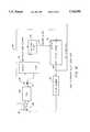
- FIG. 1Dshows the basic functional blocks in a DLL circuit 100, which may be embodied in the digital system of FIG. 1A.
- the circuitmay be digital, analog or a combination of both.
- a reference clock 102is provided from a source external to circuit 100.
- Reference clock 102is input along with an internal, or "feedback" clock 104, to PFD 106.
- PFD 106outputs signals UP 108 and DWN 110 which are input to current pump 112.
- PFD106detects frequency and phase differences between reference clock 102 andinternal clock 104.
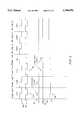
- FIG. 2shows a timing diagram of signals in the DLL circuit 100 of FIG. 1D.
- reference clock 102is shown as waveform 150
- internal clock 104is shown as waveform 152.
- the phase difference between referenceclock waveform 150 and internal clock waveform 152is shown, for example, at 154. Because internal clock waveform 152, rises from low to high, before reference clock waveform 150, the internal clock signal is said to "lead" the reference clock signal.
- the amount of lead in the internal clock waveform 152is used to generate asignal on UP signal 108.
- Signal 108is in the form of a square wave having a duration of the same interval as the lead time between clock waveforms 150 and 152.
- Signal 108is shown at 160 in the timing diagram of FIG. 2.
- the case where the internal clock waveform 152 "lags," the reference clock waveform 150is shown at 162.
- PFD 106outputs a signal on the DWN signal line to produce a square wave with a duration equivalent to the amount of lag between the clock waveforms.
- DWN signal 110is shown at 164 in the timing diagram of FIG. 2.
- the UP and DWN signals 108 and 110are input to current pump 112.
- Current pump 112sends a charge to low pass filter 114 corresponding to signals 108 and 110 from PFD 106.
- the output of low pass filter 114is an analog voltage level as shown by waveform 166of FIG. 2. This analog signal output by low pass filter 114 is shown as signal 116 in FIG. 1D.
- Signal 116is fed to delay chain 118 to control theamount of delay applied to the reference clock signal.
- the delayed reference clock signalis output at 120 to delay element 122.
- the output 120is also the clock output distributed to components on the integrated circuit in which the digital/analog DLL of FIG. 1D is acting as the clock distribution circuit.
- Delay element 122serves to further delay the already delayed reference clock signal from delay chain 118. This further delay compensates for internal delays across a chip on which the circuit is fabricated. By matching all of the delays on the chip the DLL can compensate for the worst case delay.
- the output of delay element 122is used as the input to PFD 106.
- the method of distributing the clock throughout the integrated circuitmay include programmable delay elements.
- the clock outputmay be distributed to components of an integrated circuit through a plurality of programmable delay elements.
- These programmable delay elementsmay be programmed to provide a uniform delay for the synchronized clock throughout the integrated circuit. For example, for a component a longer distance away from the clock generator, a longer programmable delay may beused that for a component closer to the clock generator. Programmable delays may be used in this way to equalize the delay and skew of the clocksignal at the various components, regardless of their distance from the clock generator.
- the programmable delay elementsmay be programmable metal elements, providing an RC delay.
- delay chain 118 and delay element 122may be implemented using programmable delay elements.
- a clock signalis routed long distances from the clock source.
- the present inventionpermits these long runs of a clock signal line, and minimizes the clock skew between the signal lines.
- a zeronanoseconds clock skewmay be obtained with the present invention.
- thismay improve, for example, the setup and hold times for components, functional blocks and I/Os on the integrated circuit.
- FIG. 3Ais a diagram of a circuit for achieving the PFD function shown in FIG. 1D's PFD 106.
- FIG. 3Ashows a digital approach to implementing a PFD.
- the circuit of 3Ais only a phase detector, since it is incapable of detecting frequency errors, as discussed below.
- An advantage to using the digital phase-only circuit detector of FIG. 3Ais that the space required to fabricate the circuit on a silicon substrate is small. Also, the circuit of FIG. 3A uses standard digital components and is easily fabricated in an integrated circuit.
- FIG. 3Ashows two flip-flops, FF1 and FF2. These flip-flops are of the D-latch type as is commonly known in the art. Each flip-flop is clocked bythe reference clock signal, REF CLK. The input to each flip-flop is derivedfrom the feedback clock signal shown as the internal clock signal 104 in FIG. 1D. FF1 receives a delayed feedback clock. The delay is due to inverters at 180. The use of two inverters is arbitrary and affects the phase error detection as discussed below. It will be apparent that any number of inverters and/or buffers may be used in place of the two inverters at 180 to create a delay for the input signal to FF1. FF2 receives the undelayed feedback clock as shown in FIG. 3A.
- FIG. 3Bis a timing diagram showing the reference clock signal, FF1 input signal and FF2 input signal, respectively, as waveforms 182, 184 and 186. Since the input to FF1, labelled “FF1 D”, is delayed with respect to the input of FF2, there is an interval, "d,” between the leading edges of eachof these waveforms as shown in FIG. 3B.
- FF1 Dthe input to FF1
- dan interval between the leading edges of eachof these waveforms as shown in FIG. 3B.
- each rising edge of the reference clockoccurs between the leading edges of the FF1 and FF2 signal inputs.
- Combinational logic at 188 in FIG. 3Areceives the outputs of FF1 and FF2 and generates a combined signal output.
- combinational logic 188could be a simple 2-input exclusive OR gate with the inputs to the exclusive OR gate being the outputs of each of FF1 and FF2.
- the output of combinational logic 188will be high, or a "1.” This is because the outputs of FF1 and FF2 will notbe the same at the leading edge of the reference clock since the reference clock goes high after FF2 has gone high and before FF1 has gone high.
- the outputs of FF1 and FF2are the same and the output of the exclusive OR gate (i.e., the output of combinational logic 188) is a low or "0" logic level.
- combinational logic 188Another possibility for combinational logic 188, is to use an AND gate to output a high logic signal when the feedback clock is leading the reference clock by a sufficient margin so that high signals on both of theFF1 and FF2 inputs are sampled.
- a NOR gatecould be used to output a logic high when the feedback clock is sufficiently lagging the reference clock so that the reference clock leading edge samples a low signal on both of the FF1 and FF2 inputs. In this latter case, there are two lines output from combinational logic 188. Many approaches, including different combinations of gates, to detect and generate a phase error signal are possible.
- the present inventionapplies digital delay lock loops (DDLL), analog delaylock loops, (ADLL), and phase lock loops (PLL), to name a few.
- DDLLdigital delay lock loops
- ADLLanalog delaylock loops
- PLLphase lock loops
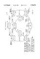
- FIG. 4shows a digital DLL (DDLL) block diagram using macro and micro phasedetectors. This circuit functions similarly to the circuits discussed abovefor a DLL, except that the phase error detection and delay selection is implemented in two separate stages amounting to a coarse and fine adjustment of the delay. Further, the circuit of FIG. 4 uses standard digital parts such as a shift register and a counter to implement the delay selection function, shown as delay chain 118 of FIG. 1D, discussed above.
- block diagram 200shows macro phase detector 202 having a REF CLK input at 204 and a feedback clock input at 206.
- Macro phase detector 202can be implemented by a circuit similar to that ofFIG. 3A discussed above. Macro phase detector 202 outputs a left/right/idlesignal 208 to shift register 210.
- the left/right/idle signalcan be one or more lines that indicate to shift register 210 whether the reference clockis leading or lagging the internal clock by at least a fixed time duration called the macro error threshold.
- Micro phase detector 218functions similarly to macro phase detector 202, except that micro detector 218 is sensitive to a smaller fixed time duration, i.e., the micro error threshold, than macro detector 202. In other words, micro phase detector 218 will have a smaller value for d, shown in FIG. 3B, so that micro phase detector 218 can be used to detect smaller phase differences between the internal, or feedback, clock and reference clock. Micro phase detector 218 outputs up/down/idle signal 222 to counter 220.
- FIGS. 8 and 9Examples of a macro phase error detector circuit and a micro phase error detector circuit are shown in FIGS. 8 and 9, respectively.
- signals NDN, NUP and IDLEimplement the left/right/idle signal 208 of FIG.4.
- the left/right/idle signalis implemented with three signals, NDN, NUP and IDLE for controlling shift register 210.
- NUPis active shift register 210 shifts right
- NDNis active shift register 210 shifts left
- IDLEactive no shifting occurs.
- the micro phase error detector circuit of FIG. 9operates similarly to the macro phase error detector circuit of FIG. 8.
- signals DN, UP and LOCKare used to, respectively, increment, decrement and preserve a count in counter 220.
- the micro phase error detector circuit of FIG. 9is provided with control signals INCWIN and DECWIN for modifying the delay "window" to make the circuit more or less sensitive to timing differences between the CLK and NREFCLK signals.
- Signals INCWIN and DECWINmay be controlled by external circuitry, such as other circuitry on the same chipas the delay lock loop circuit.
- Shift register 210along with variable macro delay 212, perform a macro delay selector function to delay the reference clock signal according to the phase error detected by macro phase detector 202.
- shift register 210is preset with a value that is shifted according to the signal 208 from macro phase detector 202.
- shift register 210can be preset with a value such as binary 11100 (or 11000; 10000) that is shifted left when macro phase detector 202 indicatesthat the feedback clock on line 206 is leading the reference clock 204.
- shift register 210could shift the preset value to the right when macro phase detector 202 indicates that the feedback clock 206 lags the reference clock 204.
- variable macro delay 212can be, e.g., a multiplexer that selects one of several delay values to apply to the reference clock input to variable macro delay212 via line 213.
- the choice of using a counter or shift register devicescan be made according to layout considerations and speed of the specific device.
- the preferred embodimentuses a shift register for the macro delayand a counter for the micro delay.
- variable macro delay 212the delayed reference clock signal is output to variable micro delay 216 via line 215.Variable micro delay 216 and counter 220 form a micro delay selector similar to the macro delay selector described above.
- Micro phase detector 218outputs the up/down/idle signal 222 to counter 220.
- Counter 220uses the signal 222 to increment or decrement a count value depending on whether the micro phase detector 218 determines that the feedback clock signal on line 230 leads, or lags, respectively, the reference clock signal on line 232. For example, if micro phase detector 218 determines that the feedback clock signal 230 leads the reference clock signal 232, then micro phase detector will output an up signal on signal 222 to directcounter 220 to increment its count value.
- variable micro delay 216selects one of several delay values to apply to the delayed reference clock on line 215. This generates a further delayed reference clock signal that is output by variable micro delay 216 onto line 217.
- CLK OUT signalis obtained from line 217 as the clock signal to be distributed to the various components on the integrated circuit for which the digital delay lock loop (DDLL) of FIG. 4 is acting as the clock distribution circuit.
- lumped delay 214receives the further delayed reference clock signal on line 217, applies a fixed delay,and outputs the feedback clock signal at 221. Lumped delay 214 matches loading seen on the chip.
- FIG. 5shows a circuit diagram where a PLL or DLL (P/DLL) generates a synchronized clock signal 302 from a reference clock signal input at pad 300 and where the synchronized or reference clocks are selectable for distribution to different parts of the integrated circuit on which the P/DLL resides.
- P/DLLPLL or DLL
- the circuit shown in FIG. 5allows either the synchronized or reference clocks to be distributed to five different areas of an integrated circuit,or chip.
- the selection of one of the clocksis performed by the five multiplexers shown as MUX 304, 306, 308, 310 and 312.
- the multiplexersareused to select one of the two clocks via control signals (not shown) which may be driven by, e.g., a register that is loadable under the direction ofa micro processor on the chip.
- Delay elements L1-5are used to match the delay across the chip. By modifying the amount of delay at each of the elements through line matching, the GCLKs can be brought into close synchronization.
- the synchronized clockis output by P/DLL circuitry in block 320 and may be, e.g., the DLL circuit discussed above in connection with FIGS. 1-4.
- FIG. 6shows the circuit of FIG. 5 with more detail in P/DLL block 320 of FIG. 5.
- FIG. 6shows that any of three synchronization approaches can be selected by using demultiplexer 350 and multiplexer 352 within P/DLL block354.
- demultiplexer 350 and multiplexer 352any of the three clocksynchronization systems shown as DDLL, ADLL and APLL may be selected.
- Theseclock synchronization systemsare, respectively, a digital delay lock loop,an analog delay lock loop and an analog phase lock loop.
- the digital delay lockmay be implemented by, e.g., a circuit as shown in FIG. 1D, and may include any of the additional circuit details discussed in FIGS. 2-4.
- the analog delay lock loopcan be implemented with the circuit as shown in FIG. 1D by using an analog design approach as is known in the art.
- the analog phase lock loopmay be implemented with an analog phase lock loop design as is known in the art.
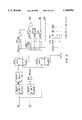
- FIG. 7is a state diagram 400 for the delay lock loop circuit of FIG. 4.
- the circuit of FIG. 4is initialized. This includes, for example, resetting shift register 210 and counter 220. Also, if the circuit of FIG. 3A is used to perform phase detection then flip-flops FF1 and FF2 may be reset. From state 402 macro phase detector 202 determines whether to shift up or down. State 404 represents the state where the feedback clock is lagging behind the reference clock so that the shift register shifts up. State 406 represents the state where the feedback clock is leading the reference clock so that the shift register shifts down.
- State 404remains the current state for as long as the circuit of FIG. 4 isin a condition where the feedback clock signal lags the reference clock signal by an amount that equals or exceeds a macro error threshold.
- the value for the macro error thresholdis 1.5 nS while the micro error threshold, or window, is 0.2 nS.
- An analogous operationpertains to state 406 where the shift register is shifted down as long as the feedback clock leads the reference clock by an amount that is greater than the macro error threshold.
- the stateprogresses from state 404 to state 414, or from state 406 to state 418.
- the micro phase detectorwill increment the counter 220 as long as the feedback clock lags the reference clock by at least the micro error threshold amount.
- the micro phase detectordecrements the counter as long as the feedback clock leads the reference clock by at least the micro error threshold amount. If the counter overflows at state 414 then states 410 and 408 are entered to reset the counter. The counter reset changes the micro delay to approximately match the delay change in the macro delay. If the counter underflows from the decrement operation at state 418 then states 412 and 408 are entered to reset the counter.
- state 404is entered if the counter hasrolled over to perform a macro adjustment to increase the delay to the feedback signal. Similarly, if the counter has rolled under then from state 408 state 406 is entered to perform a macro adjustment to decrease the delay to the feedback signal.
- state 416is entered to indicate that the feedback and reference clocks are locked together. This occurs when the phase error difference between the two clock signals is less than the micro error threshold. Should the phase error increase beyond the micro error threshold then either state 414 or state 418 is again entered depending on whether the phase error indicates that the feedback clock leads the reference clock or lags the reference clock, respectively.
Landscapes
- Physics & Mathematics (AREA)
- Engineering & Computer Science (AREA)
- Mathematical Physics (AREA)
- General Engineering & Computer Science (AREA)
- Theoretical Computer Science (AREA)
- Computer Hardware Design (AREA)
- Computing Systems (AREA)
- General Physics & Mathematics (AREA)
- Computer Networks & Wireless Communication (AREA)
- Stabilization Of Oscillater, Synchronisation, Frequency Synthesizers (AREA)
- Design And Manufacture Of Integrated Circuits (AREA)
- Pulse Circuits (AREA)
Abstract
Description
This invention relates generally to clock distribution in integrated circuits and specifically to a clock distribution scheme using a delay lock loop.
As the level of integration in semiconductor integrated circuits (ICs) increases, signal delays due to parasitic resistance-capacitance loading become larger. This is especially true of high fan-out global signal lines such as synchronous clocks. Clock signals in modern programmable logic devices may drive several thousand registers. This is a considerable load to the clock driver. Clock tree structures can be implemented on-chip to minimize clock skew among registers. However, the base trunk clock driver must be capable of driving this clock tree structure and, as a result, a buffer delay of several nanoseconds is typically incurred.
One approach to clock distribution uses a phase locked loop (PLL). This approach uses a phase-locked loop to synchronize a clock distribution signal to a reference clock signal. Since the phase-locked loop generates an internal clock signal and synchronizes it to the reference clock signal from an external source, the reference clock signal does not drive the clock tree structure.
However, some problems exist with implementing a PLL in a typical integrated circuit since the PLL uses analog devices such as a phase frequency detector (PFD), charge pump and low pass filter. These problems include, among others, poor stability and performance in a noisy environment.
It is desirable to use a circuit which achieves clock distribution while minimizing the number of components, thus reducing the area on the chip used by the clock distribution circuit.
The present invention uses a delay lock loop (DLL) which can be fabricated using digital (DDLL) or analog circuitry (ADLL). The DLL achieves advantages over the PLL. Specific embodiments of a DLL further reduce the components necessary to implement the DLL. The DLL circuit of the present invention may be used in many types of integrated circuits including memories, microprocessors, ASICs, and programmable logic devices.
In one embodiment, a DLL circuit is formed on a substrate. The DLL circuit includes a reference clock input for receiving an external reference signal; a feedback clock signal derived from the reference clock signal; a digital phase detector coupled to the reference clock signal and the feedback clock signal, wherein the digital phase detector determines the phase difference between the reference clock signal and the feedback clock signal and outputs a phase error signal at a phase error signal output.
The embodiment further includes a delay selector coupled to the phase error signal and the reference clock signal in response to the phase error signal, wherein the delay selector outputs the delayed reference clock signal as the feedback clock signal. A synchronized clock output is coupled to the feedback clock signal for outputting the synchronized clock.
Another embodiment of a DLL circuit includes a reference clock input for receiving an external reference clock signal; a feedback clock signal derived from the reference clock signal; a macro phase detector coupled to the reference clock signal and the delayed feedback signal, wherein the macro phase detector outputs a macro phase error signal indicating the phase difference between the reference clock signal and the delayed feedback signal, and wherein the macro phase error signal indicates phase differences of at least a first amount.
The second embodiment further includes a micro phase detector coupled to the reference clock signal and the delayed feedback signal, wherein the micro phase detector outputs a micro phase error signal indicating the phase difference between the reference clock signal and the delayed feedback signal. The micro phase error signal indicates phase differences of at least a second amount, wherein the second amount is smaller than the first amount.
A micro delay selector responsive to the macro phase error signal is also included for outputting a delayed reference clock signal. The circuit further includes a micro delay selector coupled to the output of a micro delay selector, wherein the micro delay selector outputs a further delayed reference clock signal; and a synchronized clock signal derived from the further delayed reference clock signal.
Other objects, features, and advantages of the present invention will become apparent upon consideration of the following detailed description and the accompanying drawings, in which like reference designations represent like features throughout the figures.
FIG. 1A is a block diagram of a digital system incorporating a programmable logic device integrated circuit;
FIG. 1B is a block diagram showing the overall architecture of a programmable logic device;
FIG. 1C is a simplified block diagram of a logic array block (LAB) of a programmable logic device;
FIG. 1D shows the basic functional blocks in a digital or analog delay lock loop circuit of the present invention;
FIG. 2 shows a timing diagram of the signals in the circuit of FIG. 1D;
FIG. 3A is a diagram of a circuit for achieving a phase frequency detector function;
FIG. 3B is a timing diagram showing a reference clock and flip-flop input waveforms;
FIG. 4 shows a delay lock loop block diagram using macro and micro phase detectors;
FIG. 5 shows a circuit diagram where synchronized or reference clocks are selectable for distribution to different parts of an integrated circuit;
FIG. 6 shows the circuit of FIG. 5 with more detail for one of the functional blocks;
FIG. 7 is a state diagram for the delay lock loop block diagram of FIG. 4;
FIG. 8 shows a macro phase error detector circuit; and
FIG. 9 shows a micro phase error detector circuit.
FIG. 1A shows a block diagram of a digital system within which the present invention may be embodied. In the particular embodiment of FIG. 1A, aprocessing unit 101A is coupled to a memory 105a and an I/O 111A and incorporates a programmable logic device (PLD) 121A. PLD 121A may be specially coupled tomemory 105A throughconnection 131A and to I/O 111A throughconnection 135A. The system may be a programmed digital computer system, digital signal processing system, specialized digital switching network, or other processing system. Moreover, the system may be a generalpurpose computer, a special purpose computer (such as telecommunications equipment) optimized for an application-specific task such as programming PLD 121A, or a combination of a general purpose computer and auxiliary special purpose hardware.
In some embodiments,processing unit 101A may even be a computer system. Inone embodiment, source code may be stored inmemory 105A, compiled into machine language, and executed byprocessing unit 101A.Processing unit 101A need not contain a CPU and in one embodiment, instructions may be executed by one ormore PLDs 121A. Instead of storing source code inmemory 105A, only the machine language representation of the source code, without the source code, may be stored inmemory 105A for execution byprocessing unit 101A.Memory 105A may be a random access memory (RAM), read only memory (ROM), fixed or flexible disk media, PC Card flash disk memory, tape, or any other storage retrieval means, or any combination of these storage retrieval means.
FIG. 1B is a simplified block diagram of the overall internal architecture and organization ofPLD 121A of FIG. 1A. Many details of PLD architecture,organization, and circuit design are not necessary for an understanding of the present invention and such details are not shown in FIG. 1B.
FIG. 1B shows a six-by-six two-dimensional array of thirty-six logic array blocks (LABs) 200A.LAB 200A is a physically grouped set of logical resources that is configured or programmed to perform logical functions. The internal architecture of a LAB will be described in more detail below in connection with FIG. 1C. PLDs may contain any arbitrary number of LABs,more or less than thePLD 121A shown in FIG. 1B. Generally, in the future, as technology advances and improves, programmable logic devices with even greater numbers of logic array blocks will undoubtedly be created. Furthermore,LABs 200A need not be organized in a square matrix; for example, the array may be organized in a five-by-seven or a twenty-by-seventy matrix of LABs.
In one embodiment,GH 210A andGV 220A conductors may or may not be programmably connectable atintersections 225A of these conductors. Moreover,GH 210A andGV 220A conductors may make multiple connections toother GH 210A andGV 220A conductors.Various GH 210A andGV 220A conductors may be programmably connected together to create a signal path from aLAB 200A at one location onPLD 121A to anotherLAB 200A at anotherlocation onPLD 121A. Furthermore, an output signal from oneLAB 200A can be directed into the inputs of one ormore LABs 200A. Also, using the global interconnect, signals from aLAB 200A can be fed back into thesameLAB 200A. In other embodiments or the present invention, only selectedGH 210A conductors are programmably connectable to a selection ofGV 220A conductors. Furthermore, in still further embodiments,GH 210A and GV 220Aconductors may be specifically used for passing signal in a specific direction, such as input or output, but not both.
The PLD architecture in FIG. 1B further shows at the peripheries of the chip, input-output drivers 230A. Input-output drivers 230A are for interfacing the PLD to external, off-chip circuitry. FIG. 1B shows thirty-two input-output drivers 230A; however, a PLD may contain any number of input-output drivers, more or less than the number depicted. Each input-output driver 230A is configurable for use as an input driver, output driver, or bidirectional driver.
FIG. 1C shows a simplified block diagram ofLAB 200A of FIG. 1B.LAB 200A is comprised of a varying number of logic elements (LEs) 300A, sometimes referred to as "logic cells," and a local (or internal)interconnect structure 310A.LAB 200A has eightLEs 300A, butLAB 200A may have any number of LEs, more or less than eight. In a further embodiment of the present invention,LAB 200A has two "banks" of eight LEs for a total of sixteen LEs, where each bank has separate inputs, outputs, control signals, and carry chains.
A general overview ofLE 300A is presented here, sufficient to provide a basic understanding of the present invention.LE 300A is the smallest logical building block of a PLD. Signals external to the LAB, such asfromGHs 210A andGVs 220A, are programmably connected toLE 300A throughlocal interconnect structure 310A, althoughLE 300A may be implemented in many architectures other than those shown in FIGS. 1A-C. In one embodiment,LE 300A of the present invention incorporates a function generator that is configurable to provide a logical function of a number of variables, such a four-variable Boolean operation. As well as combinatorial functions,LE 300A also provides support for sequential and registered functions using, for example, D flip-flops.
The present invention may be used in various places in many types of integrated circuits, including a PLD as described above. For example, in aPLD, the present invention may be used to drive a clock signal throughout the PLD components, with minimal clock skew between the components. In oneembodiment of the present invention, there is no clock skew between the components. A clock generated using the techniques of the present invention may be routed to the look-up tables, sequential machines, registers, function generators, programmable interconnect, multiplexers, I/Os and other components of the PLD.
FIG. 1D shows the basic functional blocks in aDLL circuit 100, which may be embodied in the digital system of FIG. 1A. The circuit may be digital, analog or a combination of both. In FIG. 1D, areference clock 102 is provided from a source external tocircuit 100.Reference clock 102 is input along with an internal, or "feedback"clock 104, toPFD 106. PFD 106outputs signals UP 108 andDWN 110 which are input tocurrent pump 112. PFD106 detects frequency and phase differences betweenreference clock 102andinternal clock 104.
FIG. 2 shows a timing diagram of signals in theDLL circuit 100 of FIG. 1D.In FIG. 2,reference clock 102 is shown aswaveform 150, whileinternal clock 104 is shown aswaveform 152. The phase difference betweenreferenceclock waveform 150 andinternal clock waveform 152 is shown, for example, at 154. Becauseinternal clock waveform 152, rises from low to high, beforereference clock waveform 150, the internal clock signal is said to "lead" the reference clock signal.
The amount of lead in theinternal clock waveform 152 is used to generate asignal onUP signal 108.Signal 108 is in the form of a square wave having a duration of the same interval as the lead time betweenclock waveforms Signal 108 is shown at 160 in the timing diagram of FIG. 2. Similarly, the case where theinternal clock waveform 152 "lags," thereference clock waveform 150 is shown at 162. In this case,PFD 106 outputs a signal on the DWN signal line to produce a square wave with a duration equivalent to the amount of lag between the clock waveforms. DWN signal 110 is shown at 164 in the timing diagram of FIG. 2.
Returning to FIG. 1D, the UP and DWN signals 108 and 110 respectively, are input tocurrent pump 112.Current pump 112 sends a charge tolow pass filter 114 corresponding tosignals PFD 106. The output oflow pass filter 114 is an analog voltage level as shown by waveform 166of FIG. 2. This analog signal output bylow pass filter 114 is shown assignal 116 in FIG. 1D.Signal 116 is fed to delaychain 118 to control theamount of delay applied to the reference clock signal. The delayed reference clock signal is output at 120 to delayelement 122. Theoutput 120 is also the clock output distributed to components on the integrated circuit in which the digital/analog DLL of FIG. 1D is acting as the clock distribution circuit.Delay element 122 serves to further delay the already delayed reference clock signal fromdelay chain 118. This further delay compensates for internal delays across a chip on which the circuit is fabricated. By matching all of the delays on the chip the DLL can compensate for the worst case delay. The output ofdelay element 122 is used as the input toPFD 106.
The method of distributing the clock throughout the integrated circuit may include programmable delay elements. For example, the clock output may be distributed to components of an integrated circuit through a plurality of programmable delay elements. These programmable delay elements may be programmed to provide a uniform delay for the synchronized clock throughout the integrated circuit. For example, for a component a longer distance away from the clock generator, a longer programmable delay may beused that for a component closer to the clock generator. Programmable delays may be used in this way to equalize the delay and skew of the clocksignal at the various components, regardless of their distance from the clock generator. In a preferred embodiment, the programmable delay elements may be programmable metal elements, providing an RC delay. Similarly,delay chain 118 anddelay element 122 may be implemented using programmable delay elements.
There are many benefits due to clock synthesis. For example, on many integrated circuits, a clock signal is routed long distances from the clock source. The present invention permits these long runs of a clock signal line, and minimizes the clock skew between the signal lines. A zeronanoseconds clock skew may be obtained with the present invention. By minimizing the skew between the clock lines, this may improve, for example, the setup and hold times for components, functional blocks and I/Os on the integrated circuit.
There are many ways of implementing the functional blocks of FIG. 1D. Next,some of the possible implementations are discussed as preferred embodiments.
FIG. 3A is a diagram of a circuit for achieving the PFD function shown in FIG. 1D'sPFD 106. FIG. 3A shows a digital approach to implementing a PFD.The circuit of 3A is only a phase detector, since it is incapable of detecting frequency errors, as discussed below. An advantage to using the digital phase-only circuit detector of FIG. 3A is that the space required to fabricate the circuit on a silicon substrate is small. Also, the circuit of FIG. 3A uses standard digital components and is easily fabricated in an integrated circuit.
FIG. 3A shows two flip-flops, FF1 and FF2. These flip-flops are of the D-latch type as is commonly known in the art. Each flip-flop is clocked bythe reference clock signal, REF CLK. The input to each flip-flop is derivedfrom the feedback clock signal shown as theinternal clock signal 104 in FIG. 1D. FF1 receives a delayed feedback clock. The delay is due to inverters at 180. The use of two inverters is arbitrary and affects the phase error detection as discussed below. It will be apparent that any number of inverters and/or buffers may be used in place of the two inverters at 180 to create a delay for the input signal to FF1. FF2 receives the undelayed feedback clock as shown in FIG. 3A.
FIG. 3B is a timing diagram showing the reference clock signal, FF1 input signal and FF2 input signal, respectively, aswaveforms
Combinational logic at 188 in FIG. 3A receives the outputs of FF1 and FF2 and generates a combined signal output. For example,combinational logic 188 could be a simple 2-input exclusive OR gate with the inputs to the exclusive OR gate being the outputs of each of FF1 and FF2. In this case, in normal operation when the feedback clock is synchronized to the reference clock in normal operation, the output of combinational logic 188will be high, or a "1." This is because the outputs of FF1 and FF2 will notbe the same at the leading edge of the reference clock since the reference clock goes high after FF2 has gone high and before FF1 has gone high.
However, in the case where the feedback clock is not synchronized closely to the reference clock, i.e., the phase error between the reference clock and the feedback clock is large, then the outputs of FF1 and FF2 are the same and the output of the exclusive OR gate (i.e., the output of combinational logic 188) is a low or "0" logic level.
For example, where the input to FF2 has a leading edge which does not rise until after t=1, then the reference clock leading edge samples a low signal on both the inputs to FF1 and FF2. Also, where the feedback clock is leading the reference clock sufficiently so that the leading edge of FF1 (which is delayed) occurs before t=1, the reference clock will, likewise, sample a high signal on both of the inputs to FF1 and FF2 resulting in a low logic output fromcombinational logic 188.
Another possibility forcombinational logic 188, is to use an AND gate to output a high logic signal when the feedback clock is leading the reference clock by a sufficient margin so that high signals on both of theFF1 and FF2 inputs are sampled. A NOR gate could be used to output a logic high when the feedback clock is sufficiently lagging the reference clock so that the reference clock leading edge samples a low signal on both of the FF1 and FF2 inputs. In this latter case, there are two lines output fromcombinational logic 188. Many approaches, including different combinations of gates, to detect and generate a phase error signal are possible.
The present invention applies digital delay lock loops (DDLL), analog delaylock loops, (ADLL), and phase lock loops (PLL), to name a few. An example of an embodiment with DDLL is described below.
FIG. 4 shows a digital DLL (DDLL) block diagram using macro and micro phasedetectors. This circuit functions similarly to the circuits discussed abovefor a DLL, except that the phase error detection and delay selection is implemented in two separate stages amounting to a coarse and fine adjustment of the delay. Further, the circuit of FIG. 4 uses standard digital parts such as a shift register and a counter to implement the delay selection function, shown asdelay chain 118 of FIG. 1D, discussed above. In FIG. 4, block diagram 200 showsmacro phase detector 202 having a REF CLK input at 204 and a feedback clock input at 206.
Micro phase detector 218 functions similarly tomacro phase detector 202, except that micro detector 218 is sensitive to a smaller fixed time duration, i.e., the micro error threshold, thanmacro detector 202. In other words, micro phase detector 218 will have a smaller value for d, shown in FIG. 3B, so that micro phase detector 218 can be used to detect smaller phase differences between the internal, or feedback, clock and reference clock. Micro phase detector 218 outputs up/down/idle signal 222 to counter 220.
Examples of a macro phase error detector circuit and a micro phase error detector circuit are shown in FIGS. 8 and 9, respectively. In FIG. 8, signals NDN, NUP and IDLE implement the left/right/idle signal 208 of FIG.4. The left/right/idle signal is implemented with three signals, NDN, NUP and IDLE for controllingshift register 210. When NUP isactive shift register 210 shifts right, when NDN isactive shift register 210 shifts left, when IDLE is active no shifting occurs.
The micro phase error detector circuit of FIG. 9 operates similarly to the macro phase error detector circuit of FIG. 8. In FIG. 9, signals DN, UP and LOCK are used to, respectively, increment, decrement and preserve a count incounter 220. The micro phase error detector circuit of FIG. 9 is provided with control signals INCWIN and DECWIN for modifying the delay "window" to make the circuit more or less sensitive to timing differences between the CLK and NREFCLK signals. Signals INCWIN and DECWIN may be controlled by external circuitry, such as other circuitry on the same chipas the delay lock loop circuit.
Once the delay is applied by variablemacro delay 212, the delayed reference clock signal is output to variablemicro delay 216 via line 215.Variablemicro delay 216 and counter 220 form a micro delay selector similar to the macro delay selector described above. Micro phase detector 218 outputs the up/down/idle signal 222 to counter 220.Counter 220 uses thesignal 222 to increment or decrement a count value depending on whether the micro phase detector 218 determines that the feedback clock signal online 230 leads, or lags, respectively, the reference clock signal online 232. For example, if micro phase detector 218 determines that thefeedback clock signal 230 leads thereference clock signal 232, then micro phase detector will output an up signal onsignal 222 to directcounter 220 to increment its count value.
The count value is transferred to variablemicro delay 216 alongline 219. Variablemicro delay 216 selects one of several delay values to apply to the delayed reference clock online 215. This generates a further delayed reference clock signal that is output by variablemicro delay 216 ontoline 217. Note that CLK OUT signal is obtained fromline 217 as the clock signal to be distributed to the various components on the integrated circuit for which the digital delay lock loop (DDLL) of FIG. 4 is acting as the clock distribution circuit. Finally, lumpeddelay 214 receives the further delayed reference clock signal online 217, applies a fixed delay,and outputs the feedback clock signal at 221. Lumpeddelay 214 matches loading seen on the chip.
FIG. 5 shows a circuit diagram where a PLL or DLL (P/DLL) generates asynchronized clock signal 302 from a reference clock signal input atpad 300 and where the synchronized or reference clocks are selectable for distribution to different parts of the integrated circuit on which the P/DLL resides. The advantage to this scheme is that the P/DLL is placed near the pads so that the reference clock is not delayed much before it reaches the P/DLL. For the P/DLL to work properly a very stable reference clock must be provided. If the reference clock is not stable then an external circuit can switch the P/DLL off and the reference clock can be used to directly feed the circuitry on the chip.
The circuit shown in FIG. 5 allows either the synchronized or reference clocks to be distributed to five different areas of an integrated circuit,or chip. The selection of one of the clocks is performed by the five multiplexers shown asMUX block 320 and may be, e.g., the DLL circuit discussed above in connection with FIGS. 1-4.
FIG. 6 shows the circuit of FIG. 5 with more detail in P/DLL block 320 of FIG. 5. FIG. 6 shows that any of three synchronization approaches can be selected by usingdemultiplexer 350 andmultiplexer 352 within P/DLL block354. By usingdemultiplexer 350 andmultiplexer 352, any of the three clocksynchronization systems shown as DDLL, ADLL and APLL may be selected. Theseclock synchronization systems are, respectively, a digital delay lock loop,an analog delay lock loop and an analog phase lock loop. The digital delay lock may be implemented by, e.g., a circuit as shown in FIG. 1D, and may include any of the additional circuit details discussed in FIGS. 2-4. The analog delay lock loop can be implemented with the circuit as shown in FIG. 1D by using an analog design approach as is known in the art. The analog phase lock loop may be implemented with an analog phase lock loop design as is known in the art.
FIG. 7 is a state diagram 400 for the delay lock loop circuit of FIG. 4. InFIG. 7, atstate 402 the circuit of FIG. 4 is initialized. This includes, for example, resettingshift register 210 andcounter 220. Also, if the circuit of FIG. 3A is used to perform phase detection then flip-flops FF1 and FF2 may be reset. Fromstate 402macro phase detector 202 determines whether to shift up or down.State 404 represents the state where the feedback clock is lagging behind the reference clock so that the shift register shifts up.State 406 represents the state where the feedback clock is leading the reference clock so that the shift register shifts down.
Assuming that the phase error between the feedback and reference clocks is no longer greater than the macro error threshold, the state progresses fromstate 404 tostate 414, or fromstate 406 tostate 418. Atstate 414,the micro phase detector will increment thecounter 220 as long as the feedback clock lags the reference clock by at least the micro error threshold amount. Similarly, atstate 418 the micro phase detector decrements the counter as long as the feedback clock leads the reference clock by at least the micro error threshold amount. If the counter overflows atstate 414 then states 410 and 408 are entered to reset the counter. The counter reset changes the micro delay to approximately match the delay change in the macro delay. If the counter underflows from the decrement operation atstate 418 then states 412 and 408 are entered to reset the counter. Fromstate 408,state 404 is entered if the counter hasrolled over to perform a macro adjustment to increase the delay to the feedback signal. Similarly, if the counter has rolled under then fromstate 408state 406 is entered to perform a macro adjustment to decrease the delay to the feedback signal.
Assuming, from either ofstates state 414 orstate 418 is again entered depending on whether the phase error indicates that the feedback clock leads the reference clock or lags the reference clock, respectively.
In the foregoing specification, the invention has been described with reference to a specific exemplary embodiment thereof. It will, however, beevident that various modifications and changes may be made without departing from the broader spirit and scope of the invention as set forth in the appended claims. Many such changes or modifications will be readilyapparent to one of ordinary skill in the art. The specification and drawings are, accordingly, to be regarded in an illustrative rather than arestrictive sense, the invention being limited only by the provided claims.
Claims (6)
1. A digital delay lock loop circuit for outputting a synchronized clock locked to a reference clock signal, the digital delay lock loop circuit comprising:
a reference clock input for receiving the reference clock signal;
a feedback clock signal derived from the reference clock signal;
a first digital phase detector coupled to the reference clock signal and the feedback clock signal, wherein the first digital phase detector determines a first phase difference between the reference clock signal and the feedback clock signal and outputs a first phase error signal at a first phase error signal output;
a second digital phase detector coupled to the reference clock signal and the feedback clock signal, wherein the second digital phase detector determines a second phase difference between the reference clock signal and the feedback clock signal and outputs a second phase error signal at a second phase error signal output, wherein the second phase error signal is coupled to delay the feedback clock signal in response to the second phase error signal;
a delay selector coupled to the first phase error signal and the reference clock signal for applying a delay to the reference clock signal in response to the first phase error signal, wherein the delay selector outputs a delayed reference clock signal as the feedback clock signal; and
wherein the synchronized clock output is coupled to the feedback clock signal.
2. The digital delay lock loop circuit of claim 1, further comprising:
wherein the first phase error signal indicates when the feedback clock signal leads the reference clock signal, and wherein the first phase error signal indicates when the feedback clock signal lags the reference clock signal;
wherein the delay selector includes
a shift register for shifting a value in a first direction when the first phase error signal indicates that the feedback clock signal leads the reference clock signal, and wherein the shift register shifts the value in a second direction when the first phase error signal indicates that the feedback clock signal lags the reference clock signal, wherein the shift register outputs the value on one or more output lines; and
a delay multiplexer coupled to the reference clock signal and the one or more output lines of the shift register, for applying one of a plurality of delay elements to the reference clock signal and outputting the resulting delayed signal as a delayed reference clock signal.
3. A digital delay lock loop circuit for outputting a synchronized clock locked to a reference clock signal, the digital delay lock loop circuit comprising:
a reference clock input for receiving the reference clock signal;
a macro phase detector coupled to the reference clock signal and a delayed feedback signal, wherein the macro phase detector outputs a macro phase error signal indicating the phase difference between the reference clock signal and the delayed feedback signal, wherein the macro phase error signal indicates phase differences of at least a first amount;
a micro phase detector coupled to the reference clock signal and the delayed feedback signal, wherein the micro phase detector outputs a micro phase error signal indicating the phase difference between the reference clock signal and the delayed feedback signal, wherein the micro phase error signal indicates phase differences of at least a second amount wherein the second amount is smaller than the first amount;
a macro delay selector responsive to the macro phase error signal for outputting a delayed reference clock signal;
a micro delay selector coupled to the output of the macro delay selector, wherein in response to the micro phase error signal, the micro delay selector outputs a further delayed reference clock signal; and
wherein the synchronized clock signal and said delayed feedback signal are the further delayed reference clock signal.
4. The digital delay lock loop circuit of claim 3, further comprising:
wherein the macro phase error signal indicates when the delayed feedback signal leads the reference clock signal by at least the first amount, and wherein the macro phase error signal indicates when the delayed feedback signal lags the reference clock signal by at least the first amount;
wherein the macro delay selector includes
a shift register coupled to the macro phase error signal so that a value in the shift register is shifted in response to the indication of the macro phase error signal, wherein the shift register outputs the value;
a variable macro delay coupled to the reference clock signal, wherein the variable macro delay applies a delay to the reference clock signal according to the value from the shift register to generate the delayed reference clock signal;
wherein the micro phase error signal indicates when the delayed feedback signal leads the reference clock signal by at least the second amount, and wherein the micro phase error signal indicates when the delayed feedback signal lags the reference clock signal by at least the second amount;
wherein the micro delay selector includes
a counter coupled to the micro phase error signal so that a count in the counter is changed in response to the indication of the micro phase error signal; and
a variable micro delay coupled to the delayed reference clock signal, wherein the variable micro delay applies a delay to the delayed reference clock signal according to the count from the counter to generate the further delayed reference clock signal.
5. A digital delay lock loop circuit for outputting a synchronized clock locked to a reference clock signal, the digital delay lock loop circuit comprising:
a reference clock input for receiving the reference clock signal;
a feedback clock signal derived from the reference clock signal;
a first digital phase detector coupled to the reference clock signal and the feedback clock signal, wherein the first digital phase detector determines a first phase difference between the reference clock signal and the feedback clock signal and outputs a first phase error signal at a first phase error signal output;
a second digital phase detector coupled to the reference clock signal and the feedback clock signal, wherein the second digital phase detector determines a second phase difference between the reference clock signal and the feedback clock signal and outputs a second phase error signal at a second phase error signal output, wherein the second phase error signal is coupled to delay the feedback clock signal in response to the second phase error signal;
a delay selector coupled to the first phase error signal and the reference clock signal for applying a delay to the reference clock signal in response to the first phase error signal, wherein the delay selector outputs a delayed reference clock signal as the feedback clock signal, wherein the synchronized clock output is coupled to the feedback clock signal, and
a plurality of programmable delay elements, through which the synchronized clock is distributed to components of an integrated circuit, each programmable delay element is programmed to provide a uniform delay for the synchronized clock throughout the integrated circuit.
6. A digital delay lock loop comprising:
a reference clock input, receiving a reference clock signal;
a feedback clock signal derived from the reference clock signal;
a first phase detector coupled to detect a first phase difference between the reference clock signal and the feedback clock signal;
a second phase detector coupled to detect a second phase difference between the reference clock signal and the feedback clock signal, wherein the second phase detector detects a phase difference of an amount smaller than the first phase detector;
a first delay selector, delaying the reference clock based on the first phase difference from the first phase detector, and generating a first delayed reference clock signal; and
a second delay selector, delaying the first delayed reference clock based on the second phase difference from the second phase detector, and generating a second delayed reference clock, wherein the second delayed reference clock is coupled to the feedback clock signal, whereby the second delayed reference clock is synchronized with the reference clock signal.
Priority Applications (5)
| Application Number | Priority Date | Filing Date | Title |
|---|---|---|---|
| US08/543,420US5744991A (en) | 1995-10-16 | 1995-10-16 | System for distributing clocks using a delay lock loop in a programmable logic circuit |
| US08/971,315US5963069A (en) | 1995-10-16 | 1997-11-17 | System for distributing clocks using a delay lock loop in a programmable logic circuit |
| US09/165,463US6130552A (en) | 1995-10-16 | 1998-10-02 | Programmable logic integrated circuit with on-chip DLL or PLL for clock distribution |
| US09/588,034US6292016B1 (en) | 1995-10-16 | 2000-06-05 | Programmable logic with on-chip DLL or PLL to distribute clock |
| US09/829,517US6657456B1 (en) | 1995-10-16 | 2001-04-09 | Programmable logic with on-chip DLL or PLL to distribute clock |
Applications Claiming Priority (1)
| Application Number | Priority Date | Filing Date | Title |
|---|---|---|---|
| US08/543,420US5744991A (en) | 1995-10-16 | 1995-10-16 | System for distributing clocks using a delay lock loop in a programmable logic circuit |
Related Child Applications (1)
| Application Number | Title | Priority Date | Filing Date |
|---|---|---|---|
| US08/971,315ContinuationUS5963069A (en) | 1995-10-16 | 1997-11-17 | System for distributing clocks using a delay lock loop in a programmable logic circuit |
Publications (1)
| Publication Number | Publication Date |
|---|---|
| US5744991Atrue US5744991A (en) | 1998-04-28 |
Family
ID=24167973
Family Applications (5)
| Application Number | Title | Priority Date | Filing Date |
|---|---|---|---|
| US08/543,420Expired - Fee RelatedUS5744991A (en) | 1995-10-16 | 1995-10-16 | System for distributing clocks using a delay lock loop in a programmable logic circuit |
| US08/971,315Expired - LifetimeUS5963069A (en) | 1995-10-16 | 1997-11-17 | System for distributing clocks using a delay lock loop in a programmable logic circuit |
| US09/165,463Expired - LifetimeUS6130552A (en) | 1995-10-16 | 1998-10-02 | Programmable logic integrated circuit with on-chip DLL or PLL for clock distribution |
| US09/588,034Expired - LifetimeUS6292016B1 (en) | 1995-10-16 | 2000-06-05 | Programmable logic with on-chip DLL or PLL to distribute clock |
| US09/829,517Expired - LifetimeUS6657456B1 (en) | 1995-10-16 | 2001-04-09 | Programmable logic with on-chip DLL or PLL to distribute clock |
Family Applications After (4)
| Application Number | Title | Priority Date | Filing Date |
|---|---|---|---|
| US08/971,315Expired - LifetimeUS5963069A (en) | 1995-10-16 | 1997-11-17 | System for distributing clocks using a delay lock loop in a programmable logic circuit |
| US09/165,463Expired - LifetimeUS6130552A (en) | 1995-10-16 | 1998-10-02 | Programmable logic integrated circuit with on-chip DLL or PLL for clock distribution |
| US09/588,034Expired - LifetimeUS6292016B1 (en) | 1995-10-16 | 2000-06-05 | Programmable logic with on-chip DLL or PLL to distribute clock |
| US09/829,517Expired - LifetimeUS6657456B1 (en) | 1995-10-16 | 2001-04-09 | Programmable logic with on-chip DLL or PLL to distribute clock |
Country Status (1)
| Country | Link |
|---|---|
| US (5) | US5744991A (en) |
Cited By (135)
| Publication number | Priority date | Publication date | Assignee | Title |
|---|---|---|---|---|
| US5963069A (en)* | 1995-10-16 | 1999-10-05 | Altera Corporation | System for distributing clocks using a delay lock loop in a programmable logic circuit |
| US5969552A (en)* | 1998-01-15 | 1999-10-19 | Silicon Image, Inc. | Dual loop delay-locked loop |
| US6046620A (en)* | 1997-12-18 | 2000-04-04 | Advanced Micro Devices, Inc. | Programmable delay line |
| US6047346A (en)* | 1998-02-02 | 2000-04-04 | Rambus Inc. | System for adjusting slew rate on an output of a drive circuit by enabling a plurality of pre-drivers and a plurality of output drivers |
| US6069507A (en)* | 1998-05-22 | 2000-05-30 | Silicon Magic Corporation | Circuit and method for reducing delay line length in delay-locked loops |
| US6072846A (en)* | 1996-07-22 | 2000-06-06 | Samsung Electronics, Co., Ltd. | Method and apparatus for distributing a clock signal to synchronous memory elements |
| US6092211A (en)* | 1997-08-14 | 2000-07-18 | Nec Corporation | Integrated circuit for supplying a clock signal and method for constructing the same |
| US6100721A (en)* | 1999-02-01 | 2000-08-08 | Motorola, Inc. | Circuit and method of extending the linear range of a phase frequency detector |
| US6100735A (en)* | 1998-11-19 | 2000-08-08 | Centillium Communications, Inc. | Segmented dual delay-locked loop for precise variable-phase clock generation |
| US6107826A (en)* | 1998-08-19 | 2000-08-22 | Xilinx, Inc. | Interconnect structure for FPGA with configurable delay locked loop |
| US6137334A (en)* | 1998-07-06 | 2000-10-24 | Micron Technology, Inc. | Logic circuit delay stage and delay line utilizing same |
| US6150856A (en)* | 1999-04-30 | 2000-11-21 | Micron Technology, Inc. | Delay lock loops, signal locking methods and methods of implementing delay lock loops |
| US6177844B1 (en) | 1999-01-08 | 2001-01-23 | Altera Corporation | Phase-locked loop or delay-locked loop circuitry for programmable logic devices |
| US6191613B1 (en) | 1999-07-29 | 2001-02-20 | Xilinx, Inc. | Programmable logic device with delay-locked loop |
| US6208183B1 (en)* | 1999-04-30 | 2001-03-27 | Conexant Systems, Inc. | Gated delay-locked loop for clock generation applications |
| US6218876B1 (en) | 1999-01-08 | 2001-04-17 | Altera Corporation | Phase-locked loop circuitry for programmable logic devices |
| US6252419B1 (en)* | 1999-01-08 | 2001-06-26 | Altera Corporation | LVDS interface incorporating phase-locked loop circuitry for use in programmable logic device |
| US6252443B1 (en)* | 1999-04-20 | 2001-06-26 | Infineon Technologies North America, Corp. | Delay element using a delay locked loop |
| US6275079B1 (en)* | 1999-02-25 | 2001-08-14 | Hyundai Electronics Industries Co., Ltd. | Analog delay locked loop circuit |
| US6321342B1 (en) | 1999-03-23 | 2001-11-20 | Lsi Logic Corporation | Method and apparatus for interfacing circuits that operate based upon different clock signals |
| US6326826B1 (en) | 1999-05-27 | 2001-12-04 | Silicon Image, Inc. | Wide frequency-range delay-locked loop circuit |
| US6369624B1 (en) | 1998-11-03 | 2002-04-09 | Altera Corporation | Programmable phase shift circuitry |
| US6388482B1 (en)* | 2000-06-21 | 2002-05-14 | Infineon Technologies North America Corp. | DLL lock scheme with multiple phase detection |
| US6437713B1 (en)* | 2000-10-06 | 2002-08-20 | Xilinx, Inc. | Programmable logic device having amplitude and phase modulation communication |
| US6445231B1 (en) | 2000-06-01 | 2002-09-03 | Micron Technology, Inc. | Digital dual-loop DLL design using coarse and fine loops |
| US6448820B1 (en) | 1998-11-04 | 2002-09-10 | Altera Corporation | Fast locking phase frequency detector |
| US20020157031A1 (en)* | 2001-04-19 | 2002-10-24 | Micron Technology, Inc. | Capture clock generator using master and slave delay locked loops |
| US6483886B1 (en) | 1999-01-08 | 2002-11-19 | Altera Corporation | Phase-locked loop circuitry for programmable logic devices |
| US20030012320A1 (en)* | 2001-07-11 | 2003-01-16 | Micron Technology, Inc | Delay locked loop fine tune |
| EP1125391A4 (en)* | 1998-10-27 | 2003-01-29 | Intel Corp | Phase difference magnifier |
| US6566924B2 (en)* | 2001-07-25 | 2003-05-20 | Hewlett-Packard Development Company L.P. | Parallel push algorithm detecting constraints to minimize clock skew |
| US6628154B2 (en)* | 2001-07-31 | 2003-09-30 | Cypress Semiconductor Corp. | Digitally controlled analog delay locked loop (DLL) |
| US6633185B2 (en) | 2001-10-16 | 2003-10-14 | Altera Corporation | PLL/DLL circuitry programmable for high bandwidth and low bandwidth applications |
| US20030201812A1 (en)* | 2002-04-30 | 2003-10-30 | Misao Suzuki | DLL circuit |
| US6642758B1 (en) | 1998-11-03 | 2003-11-04 | Altera Corporation | Voltage, temperature, and process independent programmable phase shift for PLL |
| US20030214339A1 (en)* | 1999-03-01 | 2003-11-20 | Yasuo Miyamoto | Timing generation circuit and method for timing generation |
| US20040075135A1 (en)* | 2000-02-24 | 2004-04-22 | Robert Plikat | Monolithcally integrated semiconductor component |
| US6727734B2 (en) | 2001-08-29 | 2004-04-27 | Micron Technology, Inc. | Variable delay circuit and method, and delay locked loop, memory device and computer system using same |
| US20040088058A1 (en)* | 2002-10-25 | 2004-05-06 | Lahoucine Ettaleb | Diagnostic for poorly tuned control loops |
| US6832173B1 (en) | 2002-07-30 | 2004-12-14 | Altera Corporation | Testing circuit and method for phase-locked loop |
| US20040257137A1 (en)* | 2003-06-20 | 2004-12-23 | Altera Corporation | Techniques for dynamically selecting phases of oscillator signals |
| US6836164B1 (en) | 1998-11-03 | 2004-12-28 | Altera Corporation | Programmable phase shift circuitry |
| US20050007166A1 (en)* | 2003-07-07 | 2005-01-13 | Samsung Electronics Co., Ltd. | Delay locked loop |
| US20050017774A1 (en)* | 2001-05-29 | 2005-01-27 | Stmicroelectronics, Inc. | Precision closed loop delay line for wide frequency data recovery |
| US20050052208A1 (en)* | 2003-09-05 | 2005-03-10 | Altera Corporation, A Corporation Of Delaware | Dual-gain loop circuitry for programmable logic device |
| US6867616B1 (en) | 2003-06-04 | 2005-03-15 | Altera Corporation | Programmable logic device serial interface having dual-use phase-locked loop circuitry |
| US20050111291A1 (en)* | 2003-10-23 | 2005-05-26 | Infineon Technologies Ag | Clock signal synchronizing device, and clock signal synchronizing method |
| US6924678B2 (en) | 2003-10-21 | 2005-08-02 | Altera Corporation | Programmable phase-locked loop circuitry for programmable logic device |
| US20050189175A1 (en)* | 2004-02-26 | 2005-09-01 | Gardner Richard J. | Ladder support apparatus and methods |
| US6959062B1 (en)* | 2000-01-28 | 2005-10-25 | Micron Technology, Inc. | Variable delay line |
| US20050265117A1 (en)* | 2000-08-18 | 2005-12-01 | Rambus Inc. | Apparatus and method for generating clock signals |
| US6996736B1 (en) | 2001-05-06 | 2006-02-07 | Altera Corporation | Programmable clock network for distributing clock signals to and between first and second sections of an integrated circuit |
| US7075365B1 (en) | 2004-04-22 | 2006-07-11 | Altera Corporation | Configurable clock network for programmable logic device |
| US7091760B1 (en) | 2004-02-25 | 2006-08-15 | Altera Corporation | DLL with adjustable phase shift using processed control signal |
| US7109765B1 (en) | 1998-11-03 | 2006-09-19 | Altera Corporation | Programmable phase shift circuitry |
| US20060220677A1 (en)* | 2005-03-31 | 2006-10-05 | Intel Corporation, A Delaware Corporation | Signal measurement systems and methods |
| US7119576B1 (en) | 2000-09-18 | 2006-10-10 | Altera Corporation | Devices and methods with programmable logic and digital signal processing regions |
| US7230495B2 (en) | 2004-04-28 | 2007-06-12 | Micron Technology, Inc. | Phase-locked loop circuits with reduced lock time |
| US20070185951A1 (en)* | 2006-02-09 | 2007-08-09 | Altera Corporation | Specialized processing block for programmable logic device |
| US20070185952A1 (en)* | 2006-02-09 | 2007-08-09 | Altera Corporation | Specialized processing block for programmable logic device |
| US7346644B1 (en) | 2000-09-18 | 2008-03-18 | Altera Corporation | Devices and methods with programmable logic and digital signal processing regions |
| US20080133627A1 (en)* | 2006-12-05 | 2008-06-05 | Altera Corporation | Large multiplier for programmable logic device |
| US7436228B1 (en) | 2005-12-22 | 2008-10-14 | Altera Corporation | Variable-bandwidth loop filter methods and apparatus |
| US7451337B1 (en)* | 2002-10-07 | 2008-11-11 | Advanced Micro Devices, Inc. | Guaranteed edge synchronization for multiple clocks |
| US20090128692A1 (en)* | 2007-11-21 | 2009-05-21 | Fujitsu Ten Limited | Video signal processing device |
| US20100052730A1 (en)* | 2005-09-23 | 2010-03-04 | Edward Grochowski | Method and apparatus for late timing transition detection |
| US20100228806A1 (en)* | 2009-03-03 | 2010-09-09 | Keone Streicher | Modular digital signal processing circuitry with optionally usable, dedicated connections between modules of the circuitry |
| US20100228807A1 (en)* | 2009-03-03 | 2010-09-09 | Altera Corporation | Digital signal processing circuitry with redundancy and bidirectional data paths |
| US7814137B1 (en) | 2007-01-09 | 2010-10-12 | Altera Corporation | Combined interpolation and decimation filter for programmable logic device |
| US7822799B1 (en) | 2006-06-26 | 2010-10-26 | Altera Corporation | Adder-rounder circuitry for specialized processing block in programmable logic device |
| US7836117B1 (en) | 2006-04-07 | 2010-11-16 | Altera Corporation | Specialized processing block for programmable logic device |
| US7865541B1 (en) | 2007-01-22 | 2011-01-04 | Altera Corporation | Configuring floating point operations in a programmable logic device |
| US7949699B1 (en) | 2007-08-30 | 2011-05-24 | Altera Corporation | Implementation of decimation filter in integrated circuit device using ram-based data storage |
| US7948267B1 (en) | 2010-02-09 | 2011-05-24 | Altera Corporation | Efficient rounding circuits and methods in configurable integrated circuit devices |
| US20110219052A1 (en)* | 2010-03-02 | 2011-09-08 | Altera Corporation | Discrete fourier transform in an integrated circuit device |
| US20110238720A1 (en)* | 2010-03-25 | 2011-09-29 | Altera Corporation | Solving linear matrices in an integrated circuit device |
| US8041759B1 (en) | 2006-02-09 | 2011-10-18 | Altera Corporation | Specialized processing block for programmable logic device |
| US8120429B1 (en) | 2006-05-19 | 2012-02-21 | Altera Corporation | Voltage-controlled oscillator methods and apparatus |
| US8244789B1 (en) | 2008-03-14 | 2012-08-14 | Altera Corporation | Normalization of floating point operations in a programmable integrated circuit device |
| US8255448B1 (en) | 2008-10-02 | 2012-08-28 | Altera Corporation | Implementing division in a programmable integrated circuit device |
| US8301681B1 (en) | 2006-02-09 | 2012-10-30 | Altera Corporation | Specialized processing block for programmable logic device |
| US8307023B1 (en) | 2008-10-10 | 2012-11-06 | Altera Corporation | DSP block for implementing large multiplier on a programmable integrated circuit device |
| US8386550B1 (en) | 2006-09-20 | 2013-02-26 | Altera Corporation | Method for configuring a finite impulse response filter in a programmable logic device |
| US8386553B1 (en) | 2006-12-05 | 2013-02-26 | Altera Corporation | Large multiplier for programmable logic device |
| US8396914B1 (en) | 2009-09-11 | 2013-03-12 | Altera Corporation | Matrix decomposition in an integrated circuit device |
| US8412756B1 (en) | 2009-09-11 | 2013-04-02 | Altera Corporation | Multi-operand floating point operations in a programmable integrated circuit device |
| US8458243B1 (en) | 2010-03-03 | 2013-06-04 | Altera Corporation | Digital signal processing circuit blocks with support for systolic finite-impulse-response digital filtering |
| US8468192B1 (en) | 2009-03-03 | 2013-06-18 | Altera Corporation | Implementing multipliers in a programmable integrated circuit device |
| US8484265B1 (en) | 2010-03-04 | 2013-07-09 | Altera Corporation | Angular range reduction in an integrated circuit device |
| US8510354B1 (en) | 2010-03-12 | 2013-08-13 | Altera Corporation | Calculation of trigonometric functions in an integrated circuit device |
| US8539016B1 (en) | 2010-02-09 | 2013-09-17 | Altera Corporation | QR decomposition in an integrated circuit device |
| US8543634B1 (en) | 2012-03-30 | 2013-09-24 | Altera Corporation | Specialized processing block for programmable integrated circuit device |
| US8577951B1 (en) | 2010-08-19 | 2013-11-05 | Altera Corporation | Matrix operations in an integrated circuit device |
| US8589463B2 (en) | 2010-06-25 | 2013-11-19 | Altera Corporation | Calculation of trigonometric functions in an integrated circuit device |
| US8620980B1 (en) | 2005-09-27 | 2013-12-31 | Altera Corporation | Programmable device with specialized multiplier blocks |
| US8626815B1 (en) | 2008-07-14 | 2014-01-07 | Altera Corporation | Configuring a programmable integrated circuit device to perform matrix multiplication |
| US8645451B2 (en) | 2011-03-10 | 2014-02-04 | Altera Corporation | Double-clocked specialized processing block in an integrated circuit device |
| US8645450B1 (en) | 2007-03-02 | 2014-02-04 | Altera Corporation | Multiplier-accumulator circuitry and methods |
| US8645449B1 (en) | 2009-03-03 | 2014-02-04 | Altera Corporation | Combined floating point adder and subtractor |
| US8650236B1 (en) | 2009-08-04 | 2014-02-11 | Altera Corporation | High-rate interpolation or decimation filter in integrated circuit device |
| US8650231B1 (en) | 2007-01-22 | 2014-02-11 | Altera Corporation | Configuring floating point operations in a programmable device |
| US8706790B1 (en) | 2009-03-03 | 2014-04-22 | Altera Corporation | Implementing mixed-precision floating-point operations in a programmable integrated circuit device |
| US8762443B1 (en) | 2011-11-15 | 2014-06-24 | Altera Corporation | Matrix operations in an integrated circuit device |
| US8812576B1 (en) | 2011-09-12 | 2014-08-19 | Altera Corporation | QR decomposition in an integrated circuit device |
| US8862650B2 (en) | 2010-06-25 | 2014-10-14 | Altera Corporation | Calculation of trigonometric functions in an integrated circuit device |
| US8886696B1 (en) | 2009-03-03 | 2014-11-11 | Altera Corporation | Digital signal processing circuitry with redundancy and ability to support larger multipliers |
| US8949298B1 (en) | 2011-09-16 | 2015-02-03 | Altera Corporation | Computing floating-point polynomials in an integrated circuit device |
| US8959137B1 (en) | 2008-02-20 | 2015-02-17 | Altera Corporation | Implementing large multipliers in a programmable integrated circuit device |
| CN104378111A (en)* | 2013-08-12 | 2015-02-25 | 龙芯中科技术有限公司 | Counter and phase-locked loop |
| US8996600B1 (en) | 2012-08-03 | 2015-03-31 | Altera Corporation | Specialized processing block for implementing floating-point multiplier with subnormal operation support |
| US9053045B1 (en) | 2011-09-16 | 2015-06-09 | Altera Corporation | Computing floating-point polynomials in an integrated circuit device |
| US9098332B1 (en) | 2012-06-01 | 2015-08-04 | Altera Corporation | Specialized processing block with fixed- and floating-point structures |
| US9189200B1 (en) | 2013-03-14 | 2015-11-17 | Altera Corporation | Multiple-precision processing block in a programmable integrated circuit device |
| US9207909B1 (en) | 2012-11-26 | 2015-12-08 | Altera Corporation | Polynomial calculations optimized for programmable integrated circuit device structures |
| US9348795B1 (en) | 2013-07-03 | 2016-05-24 | Altera Corporation | Programmable device using fixed and configurable logic to implement floating-point rounding |
| US9379687B1 (en) | 2014-01-14 | 2016-06-28 | Altera Corporation | Pipelined systolic finite impulse response filter |
| CN105932988A (en)* | 2016-04-18 | 2016-09-07 | 中国科学技术大学 | Programmable picosecond level delay pulse generation device and method |
| US9600278B1 (en) | 2011-05-09 | 2017-03-21 | Altera Corporation | Programmable device using fixed and configurable logic to implement recursive trees |
| US9684488B2 (en) | 2015-03-26 | 2017-06-20 | Altera Corporation | Combined adder and pre-adder for high-radix multiplier circuit |
| US9692429B1 (en) | 2012-11-15 | 2017-06-27 | Gsi Technology, Inc. | Systems and methods involving fast-acquisition lock features associated with phase locked loop circuitry |
| US10521229B2 (en) | 2016-12-06 | 2019-12-31 | Gsi Technology, Inc. | Computational memory cell and processing array device using memory cells |
| US10770133B1 (en) | 2016-12-06 | 2020-09-08 | Gsi Technology, Inc. | Read and write data processing circuits and methods associated with computational memory cells that provides write inhibits and read bit line pre-charge inhibits |
| US10777262B1 (en) | 2016-12-06 | 2020-09-15 | Gsi Technology, Inc. | Read data processing circuits and methods associated memory cells |
| US10847213B1 (en) | 2016-12-06 | 2020-11-24 | Gsi Technology, Inc. | Write data processing circuits and methods associated with computational memory cells |
| US10847212B1 (en) | 2016-12-06 | 2020-11-24 | Gsi Technology, Inc. | Read and write data processing circuits and methods associated with computational memory cells using two read multiplexers |
| US10854284B1 (en) | 2016-12-06 | 2020-12-01 | Gsi Technology, Inc. | Computational memory cell and processing array device with ratioless write port |
| US10860320B1 (en) | 2016-12-06 | 2020-12-08 | Gsi Technology, Inc. | Orthogonal data transposition system and method during data transfers to/from a processing array |
| US10877731B1 (en) | 2019-06-18 | 2020-12-29 | Gsi Technology, Inc. | Processing array device that performs one cycle full adder operation and bit line read/write logic features |
| US10891076B1 (en) | 2016-12-06 | 2021-01-12 | Gsi Technology, Inc. | Results processing circuits and methods associated with computational memory cells |
| US10930341B1 (en) | 2019-06-18 | 2021-02-23 | Gsi Technology, Inc. | Processing array device that performs one cycle full adder operation and bit line read/write logic features |
| US10942706B2 (en) | 2017-05-05 | 2021-03-09 | Intel Corporation | Implementation of floating-point trigonometric functions in an integrated circuit device |
| US10943648B1 (en) | 2016-12-06 | 2021-03-09 | Gsi Technology, Inc. | Ultra low VDD memory cell with ratioless write port |
| US10958272B2 (en) | 2019-06-18 | 2021-03-23 | Gsi Technology, Inc. | Computational memory cell and processing array device using complementary exclusive or memory cells |
| US10998040B2 (en) | 2016-12-06 | 2021-05-04 | Gsi Technology, Inc. | Computational memory cell and processing array device using the memory cells for XOR and XNOR computations |
| US11227653B1 (en) | 2016-12-06 | 2022-01-18 | Gsi Technology, Inc. | Storage array circuits and methods for computational memory cells |
Families Citing this family (151)
| Publication number | Priority date | Publication date | Assignee | Title |
|---|---|---|---|---|
| JP3847908B2 (en)* | 1997-07-23 | 2006-11-22 | キヤノン株式会社 | Signal processing device and clock generator |
| JP3560780B2 (en)* | 1997-07-29 | 2004-09-02 | 富士通株式会社 | Variable delay circuit and semiconductor integrated circuit device |
| JP2970845B2 (en)* | 1997-09-03 | 1999-11-02 | 日本電気株式会社 | Digital DLL circuit |
| KR100264077B1 (en)* | 1997-11-21 | 2000-08-16 | 김영환 | Clock compensator for semiconductor devices |
| US6389090B2 (en)* | 1998-02-06 | 2002-05-14 | 3Com Corporation | Digital clock/data signal recovery method and apparatus |
| US6327318B1 (en) | 1998-06-30 | 2001-12-04 | Mosaid Technologies Incorporated | Process, voltage, temperature independent switched delay compensation scheme |
| US6397374B1 (en)* | 1998-09-30 | 2002-05-28 | National Semiconductor Corporation | Zero hold time circuit for high speed bus applications |
| US6777995B1 (en)* | 1999-02-26 | 2004-08-17 | Micron Technology, Inc. | Interlaced delay-locked loops for controlling memory-circuit timing |
| JP2000306399A (en)* | 1999-04-22 | 2000-11-02 | Mitsubishi Electric Corp | Semiconductor device |
| JP4077979B2 (en)* | 1999-05-27 | 2008-04-23 | 株式会社日立製作所 | Semiconductor integrated circuit device |
| JP3304920B2 (en)* | 1999-05-31 | 2002-07-22 | 日本電気株式会社 | Semiconductor device, design apparatus and design method thereof, and storage medium storing wiring information of semiconductor device |
| US6456676B1 (en)* | 1999-08-27 | 2002-09-24 | Intel Corporation | Clock signal distribution and synchronization |
| US6487648B1 (en)* | 1999-12-15 | 2002-11-26 | Xilinx, Inc. | SDRAM controller implemented in a PLD |
| US6388464B1 (en) | 1999-12-30 | 2002-05-14 | Cypress Semiconductor Corp. | Configurable memory for programmable logic circuits |
| US6864710B1 (en)* | 1999-12-30 | 2005-03-08 | Cypress Semiconductor Corp. | Programmable logic device |
| US6594772B1 (en)* | 2000-01-14 | 2003-07-15 | Hewlett-Packard Development Company, L.P. | Clock distribution circuitry to different nodes on integrated circuit with clock coupling circuitry to maintain predetermined phase relation between output and input of adjacent nodes |
| US6417521B2 (en)* | 2000-01-19 | 2002-07-09 | Semiconductor Energy Laboratory Co., Ltd. | Transmission circuit and semiconductor device |
| GB2359706B (en) | 2000-02-28 | 2004-03-10 | Mitel Corp | Integrated data clock extractor |
| US6718477B1 (en) | 2000-03-06 | 2004-04-06 | William C. Plants | Delay locked loop for an FPGA architecture |
| US7171575B1 (en) | 2000-03-06 | 2007-01-30 | Actel Corporation | Delay locked loop for and FPGA architecture |
| US6608500B1 (en) | 2000-03-31 | 2003-08-19 | Cypress Semiconductor Corp. | I/O architecture/cell design for programmable logic device |
| US6583653B1 (en)* | 2000-03-31 | 2003-06-24 | Intel Corporation | Method and apparatus for generating a clock signal |
| KR100346835B1 (en) | 2000-05-06 | 2002-08-03 | 삼성전자 주식회사 | Semiconductor memory device implementing high speed operation of delay locked loop |
| US6462688B1 (en) | 2000-12-18 | 2002-10-08 | Marvell International, Ltd. | Direct drive programmable high speed power digital-to-analog converter |
| US6775529B1 (en) | 2000-07-31 | 2004-08-10 | Marvell International Ltd. | Active resistive summer for a transformer hybrid |
| US7194037B1 (en) | 2000-05-23 | 2007-03-20 | Marvell International Ltd. | Active replica transformer hybrid |
| US7312739B1 (en) | 2000-05-23 | 2007-12-25 | Marvell International Ltd. | Communication driver |
| US7095348B1 (en) | 2000-05-23 | 2006-08-22 | Marvell International Ltd. | Communication driver |
| US7433665B1 (en) | 2000-07-31 | 2008-10-07 | Marvell International Ltd. | Apparatus and method for converting single-ended signals to a differential signal, and transceiver employing same |
| USRE41831E1 (en) | 2000-05-23 | 2010-10-19 | Marvell International Ltd. | Class B driver |
| US7113121B1 (en) | 2000-05-23 | 2006-09-26 | Marvell International Ltd. | Communication driver |
| US6331792B1 (en)* | 2000-06-30 | 2001-12-18 | Conexant Systems, Inc. | Circuit and method for unlimited range frequency acquisition |
| US7606547B1 (en) | 2000-07-31 | 2009-10-20 | Marvell International Ltd. | Active resistance summer for a transformer hybrid |
| AU2002213444A1 (en)* | 2000-10-06 | 2002-04-15 | Flextronics Semiconductor Design, Inc. | Coherent expandable high speed interface |
| DE10051100C1 (en)* | 2000-10-14 | 2002-07-11 | Infineon Technologies Ag | Integrated semiconductor device with bridgeable input low-pass filter |
| US8103496B1 (en) | 2000-10-26 | 2012-01-24 | Cypress Semicondutor Corporation | Breakpoint control in an in-circuit emulation system |
| US7765095B1 (en) | 2000-10-26 | 2010-07-27 | Cypress Semiconductor Corporation | Conditional branching in an in-circuit emulation system |
| US8149048B1 (en) | 2000-10-26 | 2012-04-03 | Cypress Semiconductor Corporation | Apparatus and method for programmable power management in a programmable analog circuit block |
| US6724220B1 (en) | 2000-10-26 | 2004-04-20 | Cyress Semiconductor Corporation | Programmable microcontroller architecture (mixed analog/digital) |
| US8176296B2 (en) | 2000-10-26 | 2012-05-08 | Cypress Semiconductor Corporation | Programmable microcontroller architecture |
| US6326830B1 (en)* | 2000-12-29 | 2001-12-04 | Intel Corporation | Automatic clock calibration circuit |
| US20020093994A1 (en)* | 2000-12-30 | 2002-07-18 | Norm Hendrickson | Reverse data de-skew method and system |
| US20020093986A1 (en)* | 2000-12-30 | 2002-07-18 | Norm Hendrickson | Forward data de-skew method and system |
| US20020090045A1 (en)* | 2001-01-10 | 2002-07-11 | Norm Hendrickson | Digital clock recovery system |
| US7123678B2 (en) | 2001-02-01 | 2006-10-17 | Vitesse Semiconductor Corporation | RZ recovery |
| US6920552B2 (en) | 2001-03-16 | 2005-07-19 | Broadcom Corporation | Network interface with double data rate and delay locked loop |
| US6538957B2 (en) | 2001-05-14 | 2003-03-25 | Sony Computer Entertainment America Inc. | Apparatus and method for distributing a clock signal on a large scale integrated circuit |
| US6950487B2 (en)* | 2001-05-18 | 2005-09-27 | Micron Technology, Inc. | Phase splitter using digital delay locked loops |
| US7042971B1 (en)* | 2001-06-12 | 2006-05-09 | Lsi Logic Corporation | Delay-locked loop with built-in self-test of phase margin |
| US6556022B2 (en)* | 2001-06-29 | 2003-04-29 | Intel Corporation | Method and apparatus for local parameter variation compensation |
| US6798259B2 (en)* | 2001-08-03 | 2004-09-28 | Micron Technology, Inc. | System and method to improve the efficiency of synchronous mirror delays and delay locked loops |
| US6556489B2 (en)* | 2001-08-06 | 2003-04-29 | Micron Technology, Inc. | Method and apparatus for determining digital delay line entry point |
| US6714057B2 (en)* | 2001-08-28 | 2004-03-30 | Xilinx, Inc. | Multi-purpose digital frequency synthesizer circuit for a programmable logic device |
| KR100437611B1 (en)* | 2001-09-20 | 2004-06-30 | 주식회사 하이닉스반도체 | A mixed delay lock loop circuit |
| DE10148878B4 (en)* | 2001-10-04 | 2006-03-02 | Siemens Ag | System and method for transmitting digital data |
| US7406674B1 (en) | 2001-10-24 | 2008-07-29 | Cypress Semiconductor Corporation | Method and apparatus for generating microcontroller configuration information |
| US6976183B2 (en)* | 2001-11-09 | 2005-12-13 | Teradyne, Inc. | Clock architecture for a frequency-based tester |
| US8078970B1 (en) | 2001-11-09 | 2011-12-13 | Cypress Semiconductor Corporation | Graphical user interface with user-selectable list-box |
| US8042093B1 (en) | 2001-11-15 | 2011-10-18 | Cypress Semiconductor Corporation | System providing automatic source code generation for personalization and parameterization of user modules |
| US7774190B1 (en) | 2001-11-19 | 2010-08-10 | Cypress Semiconductor Corporation | Sleep and stall in an in-circuit emulation system |
| US7844437B1 (en) | 2001-11-19 | 2010-11-30 | Cypress Semiconductor Corporation | System and method for performing next placements and pruning of disallowed placements for programming an integrated circuit |
| US7770113B1 (en) | 2001-11-19 | 2010-08-03 | Cypress Semiconductor Corporation | System and method for dynamically generating a configuration datasheet |
| US8069405B1 (en) | 2001-11-19 | 2011-11-29 | Cypress Semiconductor Corporation | User interface for efficiently browsing an electronic document using data-driven tabs |
| US6971004B1 (en) | 2001-11-19 | 2005-11-29 | Cypress Semiconductor Corp. | System and method of dynamically reconfiguring a programmable integrated circuit |
| JP2003188720A (en)* | 2001-12-21 | 2003-07-04 | Mitsubishi Electric Corp | PLL circuit |
| US6650575B1 (en) | 2001-12-28 | 2003-11-18 | Netlogic Microsystems, Inc. | Programmable delay circuit within a content addressable memory |
| US6944040B1 (en) | 2001-12-28 | 2005-09-13 | Netlogic Microsystems, Inc. | Programmable delay circuit within a content addressable memory |
| US6795959B1 (en)* | 2002-03-21 | 2004-09-21 | Lattice Semiconductor Corporation | Integrated delay discriminator for use with a field-programmable gate array and a method of determining a time delay thereof |
| US8103497B1 (en) | 2002-03-28 | 2012-01-24 | Cypress Semiconductor Corporation | External interface for event architecture |
| US7308608B1 (en) | 2002-05-01 | 2007-12-11 | Cypress Semiconductor Corporation | Reconfigurable testing system and method |
| US6774667B1 (en) | 2002-05-09 | 2004-08-10 | Actel Corporation | Method and apparatus for a flexible chargepump scheme for field-programmable gate arrays |
| US6703884B2 (en) | 2002-05-30 | 2004-03-09 | Texas Instruments Incorporated | System and method for distributing a reference clock in an integrated circuit using filtered power supply line |
| US6657484B1 (en) | 2002-05-30 | 2003-12-02 | Texas Instruments Incorporated | System and method for decoupling capacitance for an integrated circuit chip |
| US7378867B1 (en) | 2002-06-04 | 2008-05-27 | Actel Corporation | Field-programmable gate array low voltage differential signaling driver utilizing two complimentary output buffers |
| US6891394B1 (en) | 2002-06-04 | 2005-05-10 | Actel Corporation | Field-programmable gate array low voltage differential signaling driver utilizing two complimentary output buffers |
| US6734703B1 (en)* | 2002-07-19 | 2004-05-11 | Xilinx, Inc. | Circuits and methods for analyzing timing characteristics of sequential logic elements |
| US6765427B1 (en) | 2002-08-08 | 2004-07-20 | Actel Corporation | Method and apparatus for bootstrapping a programmable antifuse circuit |
| US7434080B1 (en) | 2002-09-03 | 2008-10-07 | Actel Corporation | Apparatus for interfacing and testing a phase locked loop in a field programmable gate array |
| US7761845B1 (en) | 2002-09-09 | 2010-07-20 | Cypress Semiconductor Corporation | Method for parameterizing a user module |
| US6750674B1 (en) | 2002-10-02 | 2004-06-15 | Actel Corporation | Carry chain for use between logic modules in a field programmable gate array |
| US7269814B1 (en) | 2002-10-08 | 2007-09-11 | Actel Corporation | Parallel programmable antifuse field programmable gate array device (FPGA) and a method for programming and testing an antifuse FPGA |
| US6885218B1 (en) | 2002-10-08 | 2005-04-26 | Actel Corporation | Parallel programmable antifuse field programmable gate array device (FPGA) and a method for programming and testing an antifuse FPGA |
| US6727726B1 (en) | 2002-11-12 | 2004-04-27 | Actel Corporation | Field programmable gate array architecture including a buffer module and a method of distributing buffer modules in a field programmable gate array |
| KR100484252B1 (en)* | 2002-11-27 | 2005-04-22 | 주식회사 하이닉스반도체 | Dll circuit |
| KR100500925B1 (en)* | 2002-11-27 | 2005-07-14 | 주식회사 하이닉스반도체 | Low jitter dll using 2 coarse half delay line with digital phase mixer |
| US6946871B1 (en) | 2002-12-18 | 2005-09-20 | Actel Corporation | Multi-level routing architecture in a field programmable gate array having transmitters and receivers |
| US7385420B1 (en) | 2002-12-27 | 2008-06-10 | Actel Corporation | Repeatable block producing a non-uniform routing architecture in a field programmable gate array having segmented tracks |
| US6891396B1 (en) | 2002-12-27 | 2005-05-10 | Actel Corporation | Repeatable block producing a non-uniform routing architecture in a field programmable gate array having segmented tracks |
| US7020793B1 (en)* | 2003-01-31 | 2006-03-28 | Lsi Logic Corporation | Circuit for aligning signal with reference signal |
| US7107477B1 (en)* | 2003-01-31 | 2006-09-12 | Altera Corporation | Programmable logic devices with skewed clocking signals |
| US7313210B2 (en)* | 2003-02-28 | 2007-12-25 | Hewlett-Packard Development Company, L.P. | System and method for establishing a known timing relationship between two clock signals |
| US7031372B2 (en)* | 2003-04-22 | 2006-04-18 | Motorola, Inc. | Multiple user reconfigurable CDMA processor |
| US7254208B2 (en)* | 2003-05-20 | 2007-08-07 | Motorola, Inc. | Delay line based multiple frequency generator circuits for CDMA processing |
| US7114069B2 (en)* | 2003-04-22 | 2006-09-26 | Motorola, Inc. | Reconfigurable processing circuit including a delay locked loop multiple frequency generator for generating a plurality of clock signals which are configured in frequency by a control processor |
| US6838902B1 (en)* | 2003-05-28 | 2005-01-04 | Actel Corporation | Synchronous first-in/first-out block memory for a field programmable gate array |
| US6825690B1 (en) | 2003-05-28 | 2004-11-30 | Actel Corporation | Clock tree network in a field programmable gate array |
| US7375553B1 (en)* | 2003-05-28 | 2008-05-20 | Actel Corporation | Clock tree network in a field programmable gate array |
| US6867615B1 (en) | 2003-05-30 | 2005-03-15 | Actel Corporation | Dedicated input/output first in/first out module for a field programmable gate array |
| US7385419B1 (en)* | 2003-05-30 | 2008-06-10 | Actel Corporation | Dedicated input/output first in/first out module for a field programmable gate array |
| US7231537B2 (en)* | 2003-07-03 | 2007-06-12 | Micron Technology, Inc. | Fast data access mode in a memory device |
| US6990010B1 (en) | 2003-08-06 | 2006-01-24 | Actel Corporation | Deglitching circuits for a radiation-hardened static random access memory based programmable architecture |
| US20050046458A1 (en)* | 2003-08-28 | 2005-03-03 | Schroeder Charles G. | Digital delay elements constructed in a programmable logic device |
| US6995590B1 (en) | 2003-09-22 | 2006-02-07 | Altera Corporation | Hybrid phase/delay locked loop circuits and methods |
| US7009407B2 (en)* | 2004-02-19 | 2006-03-07 | Micron Technology, Inc. | Delay lock circuit having self-calibrating loop |
| US7295049B1 (en) | 2004-03-25 | 2007-11-13 | Cypress Semiconductor Corporation | Method and circuit for rapid alignment of signals |
| US7078950B2 (en)* | 2004-07-20 | 2006-07-18 | Micron Technology, Inc. | Delay-locked loop with feedback compensation |
| US7138845B2 (en) | 2004-07-22 | 2006-11-21 | Micron Technology, Inc. | Method and apparatus to set a tuning range for an analog delay |
| US8069436B2 (en) | 2004-08-13 | 2011-11-29 | Cypress Semiconductor Corporation | Providing hardware independence to automate code generation of processing device firmware |
| US7583115B2 (en) | 2004-08-26 | 2009-09-01 | Micron Technology, Inc. | Delay line off-state control with power reduction |
| US7664891B2 (en)* | 2004-12-06 | 2010-02-16 | Stmicroelectronics Inc. | Modular data transfer architecture |
| US7332976B1 (en) | 2005-02-04 | 2008-02-19 | Cypress Semiconductor Corporation | Poly-phase frequency synthesis oscillator |
| US7818705B1 (en) | 2005-04-08 | 2010-10-19 | Altera Corporation | Method and apparatus for implementing a field programmable gate array architecture with programmable clock skew |
| US7400183B1 (en) | 2005-05-05 | 2008-07-15 | Cypress Semiconductor Corporation | Voltage controlled oscillator delay cell and method |
| US7423919B2 (en)* | 2005-05-26 | 2008-09-09 | Micron Technology, Inc. | Method and system for improved efficiency of synchronous mirror delays and delay locked loops |
| US7276937B2 (en)* | 2005-07-19 | 2007-10-02 | Altera Corporation | Modular interconnect circuitry for multi-channel transceiver clock signals |
| US7312662B1 (en) | 2005-08-09 | 2007-12-25 | Marvell International Ltd. | Cascode gain boosting system and method for a transmitter |
| US7577892B1 (en) | 2005-08-25 | 2009-08-18 | Marvell International Ltd | High speed iterative decoder |
| WO2007027833A2 (en)* | 2005-09-02 | 2007-03-08 | Cypress Semiconductor Corp. | Circuit, system, and method for multiplexing signals with reduced jitter |
| KR100744069B1 (en)* | 2005-09-28 | 2007-07-30 | 주식회사 하이닉스반도체 | Delay Cell of Voltage Control Delay Line Using Digital and Analog Control |
| JP2009516414A (en)* | 2005-11-11 | 2009-04-16 | エヌエックスピー ビー ヴィ | Integrating analog-to-digital converter |
| US8085067B1 (en) | 2005-12-21 | 2011-12-27 | Cypress Semiconductor Corporation | Differential-to-single ended signal converter circuit and method |
| US8067948B2 (en) | 2006-03-27 | 2011-11-29 | Cypress Semiconductor Corporation | Input/output multiplexer bus |
| US7705628B1 (en) | 2006-03-31 | 2010-04-27 | Altera Corporation | Programmable logic device having logic elements with dedicated hardware to configure look up tables as registers |
| KR100856070B1 (en)* | 2007-03-30 | 2008-09-02 | 주식회사 하이닉스반도체 | Semiconductor memory device and driving method thereof |
| US8092083B2 (en) | 2007-04-17 | 2012-01-10 | Cypress Semiconductor Corporation | Temperature sensor with digital bandgap |
| US8130025B2 (en) | 2007-04-17 | 2012-03-06 | Cypress Semiconductor Corporation | Numerical band gap |
| US8040266B2 (en) | 2007-04-17 | 2011-10-18 | Cypress Semiconductor Corporation | Programmable sigma-delta analog-to-digital converter |
| US8026739B2 (en) | 2007-04-17 | 2011-09-27 | Cypress Semiconductor Corporation | System level interconnect with programmable switching |
| US8516025B2 (en) | 2007-04-17 | 2013-08-20 | Cypress Semiconductor Corporation | Clock driven dynamic datapath chaining |
| US7737724B2 (en) | 2007-04-17 | 2010-06-15 | Cypress Semiconductor Corporation | Universal digital block interconnection and channel routing |
| US9564902B2 (en) | 2007-04-17 | 2017-02-07 | Cypress Semiconductor Corporation | Dynamically configurable and re-configurable data path |
| US8065653B1 (en) | 2007-04-25 | 2011-11-22 | Cypress Semiconductor Corporation | Configuration of programmable IC design elements |
| US8266575B1 (en) | 2007-04-25 | 2012-09-11 | Cypress Semiconductor Corporation | Systems and methods for dynamically reconfiguring a programmable system on a chip |
| US9720805B1 (en) | 2007-04-25 | 2017-08-01 | Cypress Semiconductor Corporation | System and method for controlling a target device |
| US8049569B1 (en) | 2007-09-05 | 2011-11-01 | Cypress Semiconductor Corporation | Circuit and method for improving the accuracy of a crystal-less oscillator having dual-frequency modes |
| US7893772B1 (en) | 2007-12-03 | 2011-02-22 | Cypress Semiconductor Corporation | System and method of loading a programmable counter |
| US20090176001A1 (en)* | 2007-12-21 | 2009-07-09 | E.I. Du Pont De Nemours And Company | Soy protein products having altered characteristics |
| US7952404B2 (en) | 2008-08-15 | 2011-05-31 | Mosaid Technologies Incorporated | Apparatus and method for modeling coarse stepsize delay element and delay locked loop using same |
| US8013764B1 (en) | 2009-01-31 | 2011-09-06 | Xilinx, Inc. | Method and apparatus for shifting the bits of a wide data word |
| US9448964B2 (en) | 2009-05-04 | 2016-09-20 | Cypress Semiconductor Corporation | Autonomous control in a programmable system |
| US8228102B1 (en)* | 2010-03-03 | 2012-07-24 | Altera Corporation | Phase-locked loop architecture and clock distribution system |
| US8149038B1 (en) | 2010-03-22 | 2012-04-03 | Altera Corporation | Techniques for phase adjustment |
| CN108429800B (en) | 2010-11-22 | 2020-04-24 | 杭州硕文软件有限公司 | Mobile device |
| US8907681B2 (en)* | 2011-03-11 | 2014-12-09 | Taiwan Semiconductor Manufacturing Company, Ltd. | Timing skew characterization apparatus and method |
| US8493117B2 (en) | 2011-11-14 | 2013-07-23 | International Business Machines Corporation | Leakage tolerant delay locked loop circuit device |
| US9479151B2 (en) | 2013-10-04 | 2016-10-25 | Micron Technology, Inc. | Apparatuses and methods for controlling delay circuits during an idle state to reduce degradation of an electrical characteristic |
| TWI490515B (en)* | 2013-12-20 | 2015-07-01 | Chroma Ate Inc | Automatic test equipment and clock synchronization method |
| CN103905038B (en)* | 2014-03-24 | 2017-01-25 | 东南大学 | Periodical precomputation and skew compensation circuit and method for delaying locking loop in FPGA chip thereof |
| US9634667B2 (en)* | 2014-08-29 | 2017-04-25 | Cypress Semiconductor Corporation | Integrated circuit device with programmable analog subsystem |
| US11067630B2 (en) | 2016-04-22 | 2021-07-20 | University Of Florida Research Foundation, Incorporated | System and method for electronics timing delay calibration |
| WO2018160569A1 (en) | 2017-03-01 | 2018-09-07 | Analog Devices Global Unlimited Company | Feedforward phase noise compensation |
Citations (25)
| Publication number | Priority date | Publication date | Assignee | Title |
|---|---|---|---|---|
| US4604582A (en)* | 1985-01-04 | 1986-08-05 | Lockheed Electronics Company, Inc. | Digital phase correlator |
| US4609986A (en)* | 1984-06-14 | 1986-09-02 | Altera Corporation | Programmable logic array device using EPROM technology |
| US4617479A (en)* | 1984-05-03 | 1986-10-14 | Altera Corporation | Programmable logic array device using EPROM technology |
| US4637018A (en)* | 1984-08-29 | 1987-01-13 | Burroughs Corporation | Automatic signal delay adjustment method |
| US4677318A (en)* | 1985-04-12 | 1987-06-30 | Altera Corporation | Programmable logic storage element for programmable logic devices |
| US4689581A (en)* | 1983-11-04 | 1987-08-25 | Inmos Limited | Integrated circuit phase locked loop timing apparatus |
| US4713792A (en)* | 1985-06-06 | 1987-12-15 | Altera Corporation | Programmable macrocell using eprom or eeprom transistors for architecture control in programmable logic circuits |
| US4871930A (en)* | 1988-05-05 | 1989-10-03 | Altera Corporation | Programmable logic device with array blocks connected via programmable interconnect |
| US4899067A (en)* | 1988-07-22 | 1990-02-06 | Altera Corporation | Programmable logic devices with spare circuits for use in replacing defective circuits |
| US4912342A (en)* | 1988-05-05 | 1990-03-27 | Altera Corporation | Programmable logic device with array blocks with programmable clocking |
| US5079519A (en)* | 1991-02-14 | 1992-01-07 | Notorola, Inc. | Digital phase lock loop for a gate array |
| US5118975A (en)* | 1990-03-05 | 1992-06-02 | Thinking Machines Corporation | Digital clock buffer circuit providing controllable delay |
| US5121006A (en)* | 1991-04-22 | 1992-06-09 | Altera Corporation | Registered logic macrocell with product term allocation and adjacent product term stealing |
| US5173617A (en)* | 1988-06-27 | 1992-12-22 | Motorola, Inc. | Digital phase lock clock generator without local oscillator |
| US5204555A (en)* | 1990-04-05 | 1993-04-20 | Gazelle Microcircuits, Inc. | Logic array having high frequency internal clocking |
| US5223755A (en)* | 1990-12-26 | 1993-06-29 | Xerox Corporation | Extended frequency range variable delay locked loop for clock synchronization |
| US5241224A (en)* | 1991-04-25 | 1993-08-31 | Altera Corporation | High-density erasable programmable logic device architecture using multiplexer interconnections |
| US5260611A (en)* | 1991-09-03 | 1993-11-09 | Altera Corporation | Programmable logic array having local and long distance conductors |
| US5260608A (en)* | 1990-02-06 | 1993-11-09 | Bull, S.A. | Phase-locked loop and resulting frequency multiplier |
| US5260610A (en)* | 1991-09-03 | 1993-11-09 | Altera Corporation | Programmable logic element interconnections for programmable logic array integrated circuits |
| US5298866A (en)* | 1992-06-04 | 1994-03-29 | Kaplinsky Cecil H | Clock distribution circuit with active de-skewing |
| US5350954A (en)* | 1993-03-29 | 1994-09-27 | Altera Corporation | Macrocell with flexible product term allocation |
| US5355037A (en)* | 1992-06-15 | 1994-10-11 | Texas Instruments Incorporated | High performance digital phase locked loop |
| US5537069A (en)* | 1995-03-30 | 1996-07-16 | Intel Corporation | Apparatus and method for selecting a tap range in a digital delay line |
| US5544203A (en)* | 1993-02-17 | 1996-08-06 | Texas Instruments Incorporated | Fine resolution digital delay line with coarse and fine adjustment stages |
Family Cites Families (30)
| Publication number | Priority date | Publication date | Assignee | Title |
|---|---|---|---|---|
| US357979A (en)* | 1887-02-15 | Said coats | ||
| US4494021A (en)* | 1982-08-30 | 1985-01-15 | Xerox Corporation | Self-calibrated clock and timing signal generator for MOS/VLSI circuitry |
| US4719593A (en)* | 1984-07-09 | 1988-01-12 | Advanced Micro Devices, Inc. | Apparatus for generating digital timing waveforms |
| US4633488A (en)* | 1984-11-13 | 1986-12-30 | Digital Equipment Corporation | Phase-locked loop for MFM data recording |
| US4858178A (en)* | 1986-09-30 | 1989-08-15 | Texas Instruments Incorporated | Programmable sequence generator |
| US5133064A (en)* | 1987-04-27 | 1992-07-21 | Hitachi, Ltd. | Data processing system generating clock signal from an input clock, phase locked to the input clock and used for clocking logic devices |
| JPS6437646A (en)* | 1987-08-04 | 1989-02-08 | Nec Corp | Communication processor |
| JPH01137646A (en)* | 1987-11-25 | 1989-05-30 | Hitachi Ltd | Integrated circuit |
| US5349544A (en)* | 1988-06-15 | 1994-09-20 | Advanced Micro Devices, Inc. | Programmable system synchronizer |
| US4959646A (en)* | 1988-06-17 | 1990-09-25 | Dallas Semiconductor Corporation | Dynamic PLA timing circuit |
| US4868522A (en)* | 1988-12-13 | 1989-09-19 | Gazelle Microcircuits, Inc. | Clock signal distribution device |
| US5075575A (en)* | 1989-12-11 | 1991-12-24 | Fuji Photo Film Co., Ltd. | Externally synchronized programmable device |
| US5072195A (en)* | 1990-04-05 | 1991-12-10 | Gazelle Microcircuits, Inc. | Phase-locked loop with clamped voltage-controlled oscillator |
| US5218314A (en)* | 1992-05-29 | 1993-06-08 | National Semiconductor Corporation | High resolution, multi-frequency digital phase-locked loop |
| JP2792801B2 (en)* | 1992-12-28 | 1998-09-03 | 三菱電機株式会社 | Semiconductor integrated circuit, design method and manufacturing method thereof |
| US5355035A (en)* | 1993-01-08 | 1994-10-11 | Vora Madhukar B | High speed BICMOS switches and multiplexers |
| US5644251A (en)* | 1993-04-22 | 1997-07-01 | Lsi Logic Corporation | Switchable pull-ups and pull-downs for IDDQ testing of integrated circuits |
| JPH0774596A (en)* | 1993-08-31 | 1995-03-17 | Mitsubishi Electric Corp | Ring oscillator |
| US5579353A (en)* | 1993-10-12 | 1996-11-26 | Texas Instruments Incorporated | Dynamic clock mode switch |
| US5506878A (en)* | 1994-07-18 | 1996-04-09 | Xilinx, Inc. | Programmable clock having programmable delay and duty cycle based on a user-supplied reference clock |
| US5815016A (en)* | 1994-09-02 | 1998-09-29 | Xilinx, Inc. | Phase-locked delay loop for clock correction |
| US5646564A (en)* | 1994-09-02 | 1997-07-08 | Xilinx, Inc. | Phase-locked delay loop for clock correction |
| US5777360A (en)* | 1994-11-02 | 1998-07-07 | Lsi Logic Corporation | Hexagonal field programmable gate array architecture |
| US5635857A (en)* | 1994-12-08 | 1997-06-03 | Unisys Corporation | IC chip using a common multiplexor logic element for performing logic operations |
| US5742180A (en)* | 1995-02-10 | 1998-04-21 | Massachusetts Institute Of Technology | Dynamically programmable gate array with multiple contexts |
| US5744991A (en)* | 1995-10-16 | 1998-04-28 | Altera Corporation | System for distributing clocks using a delay lock loop in a programmable logic circuit |
| US5864564A (en)* | 1995-11-17 | 1999-01-26 | Sun Microsystems, Inc. | Control circuit for deterministic stopping of an integrated circuit internal clock |
| US6107826A (en)* | 1998-08-19 | 2000-08-22 | Xilinx, Inc. | Interconnect structure for FPGA with configurable delay locked loop |
| US6218876B1 (en)* | 1999-01-08 | 2001-04-17 | Altera Corporation | Phase-locked loop circuitry for programmable logic devices |
| US6487648B1 (en)* | 1999-12-15 | 2002-11-26 | Xilinx, Inc. | SDRAM controller implemented in a PLD |
- 1995
- 1995-10-16USUS08/543,420patent/US5744991A/ennot_activeExpired - Fee Related
- 1997
- 1997-11-17USUS08/971,315patent/US5963069A/ennot_activeExpired - Lifetime
- 1998
- 1998-10-02USUS09/165,463patent/US6130552A/ennot_activeExpired - Lifetime
- 2000
- 2000-06-05USUS09/588,034patent/US6292016B1/ennot_activeExpired - Lifetime
- 2001
- 2001-04-09USUS09/829,517patent/US6657456B1/ennot_activeExpired - Lifetime
Patent Citations (26)
| Publication number | Priority date | Publication date | Assignee | Title |
|---|---|---|---|---|
| US4689581A (en)* | 1983-11-04 | 1987-08-25 | Inmos Limited | Integrated circuit phase locked loop timing apparatus |
| US4617479A (en)* | 1984-05-03 | 1986-10-14 | Altera Corporation | Programmable logic array device using EPROM technology |
| US4617479B1 (en)* | 1984-05-03 | 1993-09-21 | Altera Semiconductor Corp. | Programmable logic array device using eprom technology |
| US4609986A (en)* | 1984-06-14 | 1986-09-02 | Altera Corporation | Programmable logic array device using EPROM technology |
| US4637018A (en)* | 1984-08-29 | 1987-01-13 | Burroughs Corporation | Automatic signal delay adjustment method |
| US4604582A (en)* | 1985-01-04 | 1986-08-05 | Lockheed Electronics Company, Inc. | Digital phase correlator |
| US4677318A (en)* | 1985-04-12 | 1987-06-30 | Altera Corporation | Programmable logic storage element for programmable logic devices |
| US4713792A (en)* | 1985-06-06 | 1987-12-15 | Altera Corporation | Programmable macrocell using eprom or eeprom transistors for architecture control in programmable logic circuits |
| US4871930A (en)* | 1988-05-05 | 1989-10-03 | Altera Corporation | Programmable logic device with array blocks connected via programmable interconnect |
| US4912342A (en)* | 1988-05-05 | 1990-03-27 | Altera Corporation | Programmable logic device with array blocks with programmable clocking |
| US5173617A (en)* | 1988-06-27 | 1992-12-22 | Motorola, Inc. | Digital phase lock clock generator without local oscillator |
| US4899067A (en)* | 1988-07-22 | 1990-02-06 | Altera Corporation | Programmable logic devices with spare circuits for use in replacing defective circuits |
| US5260608A (en)* | 1990-02-06 | 1993-11-09 | Bull, S.A. | Phase-locked loop and resulting frequency multiplier |
| US5118975A (en)* | 1990-03-05 | 1992-06-02 | Thinking Machines Corporation | Digital clock buffer circuit providing controllable delay |
| US5204555A (en)* | 1990-04-05 | 1993-04-20 | Gazelle Microcircuits, Inc. | Logic array having high frequency internal clocking |
| US5223755A (en)* | 1990-12-26 | 1993-06-29 | Xerox Corporation | Extended frequency range variable delay locked loop for clock synchronization |
| US5079519A (en)* | 1991-02-14 | 1992-01-07 | Notorola, Inc. | Digital phase lock loop for a gate array |
| US5121006A (en)* | 1991-04-22 | 1992-06-09 | Altera Corporation | Registered logic macrocell with product term allocation and adjacent product term stealing |
| US5241224A (en)* | 1991-04-25 | 1993-08-31 | Altera Corporation | High-density erasable programmable logic device architecture using multiplexer interconnections |
| US5260611A (en)* | 1991-09-03 | 1993-11-09 | Altera Corporation | Programmable logic array having local and long distance conductors |
| US5260610A (en)* | 1991-09-03 | 1993-11-09 | Altera Corporation | Programmable logic element interconnections for programmable logic array integrated circuits |
| US5298866A (en)* | 1992-06-04 | 1994-03-29 | Kaplinsky Cecil H | Clock distribution circuit with active de-skewing |
| US5355037A (en)* | 1992-06-15 | 1994-10-11 | Texas Instruments Incorporated | High performance digital phase locked loop |
| US5544203A (en)* | 1993-02-17 | 1996-08-06 | Texas Instruments Incorporated | Fine resolution digital delay line with coarse and fine adjustment stages |
| US5350954A (en)* | 1993-03-29 | 1994-09-27 | Altera Corporation | Macrocell with flexible product term allocation |
| US5537069A (en)* | 1995-03-30 | 1996-07-16 | Intel Corporation | Apparatus and method for selecting a tap range in a digital delay line |
Non-Patent Citations (10)
| Title |
|---|
| Dr. Dao Long Chen, Designing On Chip Clock Generators, Circuits and Devices, Jul. 1992, pp. 32 36.* |
| Dr. Dao-Long Chen, "Designing On-Chip Clock Generators," Circuits and Devices, Jul. 1992, pp. 32-36. |
| Florence Lee, "PLL Application Note," LSI Logic Corporation, Nov. 8, 1991, pp. 1-28. |
| Florence Lee, PLL Application Note, LSI Logic Corporation, Nov. 8, 1991, pp. 1 28.* |
| Ian A. Young, Jeffrey K. Greason, Keng L. Wong, "A PLL Clock Generator with 5 to 110 MHz of Lock Range for Microprocessors," IEEE Journal of Solid State Circuits, vol. 27, No. 11, Nov. 1992, pp. 1599-1607. |
| Ian A. Young, Jeffrey K. Greason, Keng L. Wong, A PLL Clock Generator with 5 to 110 MHz of Lock Range for Microprocessors, IEEE Journal of Solid State Circuits, vol. 27, No. 11, Nov. 1992, pp. 1599 1607.* |
| Mark G. Johnson, Edwin L. Hudson, "A Variable Delay Line PLL for CPU-Coprocessor Synchronization," IEEE Journal of Solid State Circuits, vol. 23 No. 5, pp. 1218-1223. |
| Mark G. Johnson, Edwin L. Hudson, A Variable Delay Line PLL for CPU Coprocessor Synchronization, IEEE Journal of Solid State Circuits, vol. 23 No. 5, pp. 1218 1223.* |
| Uming Ko, Shannon A Wichman, Shawn Castrianni, "A 30-ps Jitter, 3.6-us Locking 3.3-Volt Digital PLL for CMOS Gate Arrays," IEEE 1993 Custom Integrated Circuits Conference, pp. 23.3.1-23.3.4. |
| Uming Ko, Shannon A Wichman, Shawn Castrianni, A 30 ps Jitter, 3.6 us Locking 3.3 Volt Digital PLL for CMOS Gate Arrays, IEEE 1993 Custom Integrated Circuits Conference, pp. 23.3.1 23.3.4.* |
Cited By (216)
| Publication number | Priority date | Publication date | Assignee | Title |
|---|---|---|---|---|
| US6292016B1 (en) | 1995-10-16 | 2001-09-18 | Altera Corporation | Programmable logic with on-chip DLL or PLL to distribute clock |
| US5963069A (en)* | 1995-10-16 | 1999-10-05 | Altera Corporation | System for distributing clocks using a delay lock loop in a programmable logic circuit |
| US6657456B1 (en) | 1995-10-16 | 2003-12-02 | Altera Corporation | Programmable logic with on-chip DLL or PLL to distribute clock |
| US6130552A (en)* | 1995-10-16 | 2000-10-10 | Altera Corporation | Programmable logic integrated circuit with on-chip DLL or PLL for clock distribution |
| US6072846A (en)* | 1996-07-22 | 2000-06-06 | Samsung Electronics, Co., Ltd. | Method and apparatus for distributing a clock signal to synchronous memory elements |
| US6092211A (en)* | 1997-08-14 | 2000-07-18 | Nec Corporation | Integrated circuit for supplying a clock signal and method for constructing the same |
| US6046620A (en)* | 1997-12-18 | 2000-04-04 | Advanced Micro Devices, Inc. | Programmable delay line |
| US5969552A (en)* | 1998-01-15 | 1999-10-19 | Silicon Image, Inc. | Dual loop delay-locked loop |
| US6047346A (en)* | 1998-02-02 | 2000-04-04 | Rambus Inc. | System for adjusting slew rate on an output of a drive circuit by enabling a plurality of pre-drivers and a plurality of output drivers |
| US6069507A (en)* | 1998-05-22 | 2000-05-30 | Silicon Magic Corporation | Circuit and method for reducing delay line length in delay-locked loops |
| US6392458B1 (en) | 1998-07-06 | 2002-05-21 | Micron Technology, Inc. | Method and apparatus for digital delay locked loop circuits |
| US6137334A (en)* | 1998-07-06 | 2000-10-24 | Micron Technology, Inc. | Logic circuit delay stage and delay line utilizing same |
| US6359482B1 (en) | 1998-07-06 | 2002-03-19 | Micron Technology, Inc. | Method and apparatus for digital delay locked loop circuits |
| US6107826A (en)* | 1998-08-19 | 2000-08-22 | Xilinx, Inc. | Interconnect structure for FPGA with configurable delay locked loop |
| EP1125391A4 (en)* | 1998-10-27 | 2003-01-29 | Intel Corp | Phase difference magnifier |
| US7109765B1 (en) | 1998-11-03 | 2006-09-19 | Altera Corporation | Programmable phase shift circuitry |
| US7358783B1 (en) | 1998-11-03 | 2008-04-15 | Altera Corporation | Voltage, temperature, and process independent programmable phase shift for PLL |
| US6642758B1 (en) | 1998-11-03 | 2003-11-04 | Altera Corporation | Voltage, temperature, and process independent programmable phase shift for PLL |
| US6667641B1 (en)* | 1998-11-03 | 2003-12-23 | Altera Corporation | Programmable phase shift circuitry |
| US6836164B1 (en) | 1998-11-03 | 2004-12-28 | Altera Corporation | Programmable phase shift circuitry |
| US6369624B1 (en) | 1998-11-03 | 2002-04-09 | Altera Corporation | Programmable phase shift circuitry |
| US6617884B2 (en) | 1998-11-04 | 2003-09-09 | Altera Corporation | Fast locking phase frequency detector |
| US6448820B1 (en) | 1998-11-04 | 2002-09-10 | Altera Corporation | Fast locking phase frequency detector |
| US6100735A (en)* | 1998-11-19 | 2000-08-08 | Centillium Communications, Inc. | Segmented dual delay-locked loop for precise variable-phase clock generation |
| US6469553B1 (en) | 1999-01-08 | 2002-10-22 | Altera Corporation | Phase-locked loop circuitry for programmable logic devices |
| US7190755B1 (en)* | 1999-01-08 | 2007-03-13 | Altera Corporation | Phase-locked loop circuitry for programmable logic devices |
| US6373278B1 (en) | 1999-01-08 | 2002-04-16 | Altera Corporation | LVDS interface incorporating phase-locked loop circuitry for use in programmable logic device |
| US6252419B1 (en)* | 1999-01-08 | 2001-06-26 | Altera Corporation | LVDS interface incorporating phase-locked loop circuitry for use in programmable logic device |
| US6271729B2 (en) | 1999-01-08 | 2001-08-07 | Altera Corporation | Phase-locked loop or delay-locked loop circuitry for programmable logic devices |
| US6437650B1 (en) | 1999-01-08 | 2002-08-20 | Altera Corporation | Phase-locked loop or delay-locked loop circuitry for programmable logic devices |
| US6483886B1 (en) | 1999-01-08 | 2002-11-19 | Altera Corporation | Phase-locked loop circuitry for programmable logic devices |
| US6177844B1 (en) | 1999-01-08 | 2001-01-23 | Altera Corporation | Phase-locked loop or delay-locked loop circuitry for programmable logic devices |
| US6218876B1 (en) | 1999-01-08 | 2001-04-17 | Altera Corporation | Phase-locked loop circuitry for programmable logic devices |
| US6100721A (en)* | 1999-02-01 | 2000-08-08 | Motorola, Inc. | Circuit and method of extending the linear range of a phase frequency detector |
| US6275079B1 (en)* | 1999-02-25 | 2001-08-14 | Hyundai Electronics Industries Co., Ltd. | Analog delay locked loop circuit |
| US20030214339A1 (en)* | 1999-03-01 | 2003-11-20 | Yasuo Miyamoto | Timing generation circuit and method for timing generation |
| US6891416B2 (en)* | 1999-03-01 | 2005-05-10 | Sharp Kabushiki Kaisha | Timing generation circuit and method for timing generation |
| US6321342B1 (en) | 1999-03-23 | 2001-11-20 | Lsi Logic Corporation | Method and apparatus for interfacing circuits that operate based upon different clock signals |
| US6252443B1 (en)* | 1999-04-20 | 2001-06-26 | Infineon Technologies North America, Corp. | Delay element using a delay locked loop |
| US6150856A (en)* | 1999-04-30 | 2000-11-21 | Micron Technology, Inc. | Delay lock loops, signal locking methods and methods of implementing delay lock loops |
| US6208183B1 (en)* | 1999-04-30 | 2001-03-27 | Conexant Systems, Inc. | Gated delay-locked loop for clock generation applications |
| US6326826B1 (en) | 1999-05-27 | 2001-12-04 | Silicon Image, Inc. | Wide frequency-range delay-locked loop circuit |
| US6191613B1 (en) | 1999-07-29 | 2001-02-20 | Xilinx, Inc. | Programmable logic device with delay-locked loop |
| US6959062B1 (en)* | 2000-01-28 | 2005-10-25 | Micron Technology, Inc. | Variable delay line |
| US20040075135A1 (en)* | 2000-02-24 | 2004-04-22 | Robert Plikat | Monolithcally integrated semiconductor component |
| US6774690B2 (en) | 2000-06-01 | 2004-08-10 | Micron Technology, Inc. | Digital dual-loop DLL design using coarse and fine loops |
| US6445231B1 (en) | 2000-06-01 | 2002-09-03 | Micron Technology, Inc. | Digital dual-loop DLL design using coarse and fine loops |
| US6388482B1 (en)* | 2000-06-21 | 2002-05-14 | Infineon Technologies North America Corp. | DLL lock scheme with multiple phase detection |
| US20050265117A1 (en)* | 2000-08-18 | 2005-12-01 | Rambus Inc. | Apparatus and method for generating clock signals |
| US7346644B1 (en) | 2000-09-18 | 2008-03-18 | Altera Corporation | Devices and methods with programmable logic and digital signal processing regions |
| US7119576B1 (en) | 2000-09-18 | 2006-10-10 | Altera Corporation | Devices and methods with programmable logic and digital signal processing regions |
| US6437713B1 (en)* | 2000-10-06 | 2002-08-20 | Xilinx, Inc. | Programmable logic device having amplitude and phase modulation communication |
| US20020157031A1 (en)* | 2001-04-19 | 2002-10-24 | Micron Technology, Inc. | Capture clock generator using master and slave delay locked loops |
| US6839860B2 (en) | 2001-04-19 | 2005-01-04 | Mircon Technology, Inc. | Capture clock generator using master and slave delay locked loops |
| US20050083099A1 (en)* | 2001-04-19 | 2005-04-21 | Micron Technology, Inc. | Capture clock generator using master and slave delay locked loops |
| US6996736B1 (en) | 2001-05-06 | 2006-02-07 | Altera Corporation | Programmable clock network for distributing clock signals to and between first and second sections of an integrated circuit |
| US6985016B2 (en)* | 2001-05-29 | 2006-01-10 | Stmicroelectronics, Inc. | Precision closed loop delay line for wide frequency data recovery |
| US20050017774A1 (en)* | 2001-05-29 | 2005-01-27 | Stmicroelectronics, Inc. | Precision closed loop delay line for wide frequency data recovery |
| US7072433B2 (en) | 2001-07-11 | 2006-07-04 | Micron Technology, Inc. | Delay locked loop fine tune |
| US20060237473A1 (en)* | 2001-07-11 | 2006-10-26 | Micron Technology, Inc. | Delay locked loop fine tune |
| US20030012320A1 (en)* | 2001-07-11 | 2003-01-16 | Micron Technology, Inc | Delay locked loop fine tune |
| US6566924B2 (en)* | 2001-07-25 | 2003-05-20 | Hewlett-Packard Development Company L.P. | Parallel push algorithm detecting constraints to minimize clock skew |
| US6628154B2 (en)* | 2001-07-31 | 2003-09-30 | Cypress Semiconductor Corp. | Digitally controlled analog delay locked loop (DLL) |
| US6759883B2 (en) | 2001-08-29 | 2004-07-06 | Micron Technology, Inc. | Variable delay circuit and method, and delay locked loop, memory device and computer system using same |
| US6735148B2 (en) | 2001-08-29 | 2004-05-11 | Micron Technology, Inc. | Variable delay circuit and method, and delay locked loop, memory device and computer system using same |
| US6850107B2 (en) | 2001-08-29 | 2005-02-01 | Micron Technology, Inc. | Variable delay circuit and method, and delay locked loop, memory device and computer system using same |
| US6727734B2 (en) | 2001-08-29 | 2004-04-27 | Micron Technology, Inc. | Variable delay circuit and method, and delay locked loop, memory device and computer system using same |
| US6812756B2 (en) | 2001-10-16 | 2004-11-02 | Altera Corporation | PLL/DLL circuitry programmable for high bandwidth and low bandwidth applications |
| US20040056695A1 (en)* | 2001-10-16 | 2004-03-25 | Greg Starr | PLL/DLL circuitry programmable for high bandwidth and low bandwidth applications |
| US6633185B2 (en) | 2001-10-16 | 2003-10-14 | Altera Corporation | PLL/DLL circuitry programmable for high bandwidth and low bandwidth applications |
| US7023251B2 (en) | 2001-10-16 | 2006-04-04 | Altera Corporation | PLL/DLL circuitry programmable for high bandwidth and low bandwidth applications |
| US20050017775A1 (en)* | 2001-10-16 | 2005-01-27 | Greg Starr | PLL/DLL circuitry programmable for high bandwidth and low bandwidth applications |
| US6949966B2 (en) | 2002-04-30 | 2005-09-27 | Elpida Memory, Inc. | DLL circuit capable of preventing malfunctioning causing locking in an antiphase state |
| US20030201812A1 (en)* | 2002-04-30 | 2003-10-30 | Misao Suzuki | DLL circuit |
| US20050046455A1 (en)* | 2002-04-30 | 2005-03-03 | Misao Suzuki | DLL circuit |
| US6812759B2 (en)* | 2002-04-30 | 2004-11-02 | Elpida Memory, Inc. | DLL circuit capable of preventing locking in an antiphase state |
| US6832173B1 (en) | 2002-07-30 | 2004-12-14 | Altera Corporation | Testing circuit and method for phase-locked loop |
| US7451337B1 (en)* | 2002-10-07 | 2008-11-11 | Advanced Micro Devices, Inc. | Guaranteed edge synchronization for multiple clocks |
| US20040088058A1 (en)* | 2002-10-25 | 2004-05-06 | Lahoucine Ettaleb | Diagnostic for poorly tuned control loops |
| US6867616B1 (en) | 2003-06-04 | 2005-03-15 | Altera Corporation | Programmable logic device serial interface having dual-use phase-locked loop circuitry |
| US20040257137A1 (en)* | 2003-06-20 | 2004-12-23 | Altera Corporation | Techniques for dynamically selecting phases of oscillator signals |
| US6933761B2 (en) | 2003-06-20 | 2005-08-23 | Altera Corporation | Techniques for dynamically selecting phases of oscillator signals |
| US20050007166A1 (en)* | 2003-07-07 | 2005-01-13 | Samsung Electronics Co., Ltd. | Delay locked loop |
| US7034590B2 (en)* | 2003-07-07 | 2006-04-25 | Samsung Electronics Co., Ltd. | Delay locked loop circuits and methods preventing erroneous transition from coarse lock to fine lock due to noise or jitter |
| US7019570B2 (en)* | 2003-09-05 | 2006-03-28 | Altera Corporation | Dual-gain loop circuitry for programmable logic device |
| US20050052208A1 (en)* | 2003-09-05 | 2005-03-10 | Altera Corporation, A Corporation Of Delaware | Dual-gain loop circuitry for programmable logic device |
| GB2405756B (en)* | 2003-09-05 | 2006-05-03 | Altera Corp | Dual-gain loop circuitry for programmable device |
| US7071743B2 (en) | 2003-10-21 | 2006-07-04 | Altera Corporation | Programmable phase-locked loop circuitry for programmable logic device |
| US6924678B2 (en) | 2003-10-21 | 2005-08-02 | Altera Corporation | Programmable phase-locked loop circuitry for programmable logic device |
| US20060158233A1 (en)* | 2003-10-21 | 2006-07-20 | Gregory Starr | Programmable phase-locked loop circuitry for programmable logic device |
| US20050206415A1 (en)* | 2003-10-21 | 2005-09-22 | Altera Corporation, A Corporation Of Delaware | Programmable phase-locked loop circuitry for programmable logic device |
| US7307459B2 (en) | 2003-10-21 | 2007-12-11 | Altera Corporation | Programmable phase-locked loop circuitry for programmable logic device |
| US7230462B2 (en)* | 2003-10-23 | 2007-06-12 | Infineon Technologies Ag | Clock signal synchronizing device, and clock signal synchronizing method |
| US20050111291A1 (en)* | 2003-10-23 | 2005-05-26 | Infineon Technologies Ag | Clock signal synchronizing device, and clock signal synchronizing method |
| US7212054B1 (en) | 2004-02-25 | 2007-05-01 | Altera Corporation | DLL with adjustable phase shift using processed control signal |
| US7091760B1 (en) | 2004-02-25 | 2006-08-15 | Altera Corporation | DLL with adjustable phase shift using processed control signal |
| US20050189175A1 (en)* | 2004-02-26 | 2005-09-01 | Gardner Richard J. | Ladder support apparatus and methods |
| US8072260B1 (en) | 2004-04-22 | 2011-12-06 | Altera Corporation | Configurable clock network for programmable logic device |
| US9490812B1 (en) | 2004-04-22 | 2016-11-08 | Altera Corporation | Configurable clock network for programmable logic device |
| US8680913B1 (en) | 2004-04-22 | 2014-03-25 | Altera Corporation | Configurable clock network for programmable logic device |
| US7646237B1 (en) | 2004-04-22 | 2010-01-12 | Altera Corporation | Configurable clock network for programmable logic device |
| US7286007B1 (en) | 2004-04-22 | 2007-10-23 | Altera Corporation | Configurable clock network for programmable logic device |
| US7859329B1 (en) | 2004-04-22 | 2010-12-28 | Altera Corporation | Configurable clock network for programmable logic device |
| US8441314B1 (en) | 2004-04-22 | 2013-05-14 | Altera Corporation | Configurable clock network for programmable logic device |
| US8253484B1 (en) | 2004-04-22 | 2012-08-28 | Altera Corporation | Configurable clock network for programmable logic device |
| US7075365B1 (en) | 2004-04-22 | 2006-07-11 | Altera Corporation | Configurable clock network for programmable logic device |
| US7230495B2 (en) | 2004-04-28 | 2007-06-12 | Micron Technology, Inc. | Phase-locked loop circuits with reduced lock time |
| US7262632B2 (en)* | 2005-03-31 | 2007-08-28 | Intel Corporation | Signal measurement systems and methods |
| US20060220677A1 (en)* | 2005-03-31 | 2006-10-05 | Intel Corporation, A Delaware Corporation | Signal measurement systems and methods |
| US20100052730A1 (en)* | 2005-09-23 | 2010-03-04 | Edward Grochowski | Method and apparatus for late timing transition detection |
| US8125246B2 (en)* | 2005-09-23 | 2012-02-28 | Intel Corporation | Method and apparatus for late timing transition detection |
| US8620980B1 (en) | 2005-09-27 | 2013-12-31 | Altera Corporation | Programmable device with specialized multiplier blocks |
| US7436228B1 (en) | 2005-12-22 | 2008-10-14 | Altera Corporation | Variable-bandwidth loop filter methods and apparatus |
| US8301681B1 (en) | 2006-02-09 | 2012-10-30 | Altera Corporation | Specialized processing block for programmable logic device |
| US8266199B2 (en) | 2006-02-09 | 2012-09-11 | Altera Corporation | Specialized processing block for programmable logic device |
| US8266198B2 (en) | 2006-02-09 | 2012-09-11 | Altera Corporation | Specialized processing block for programmable logic device |
| US20070185952A1 (en)* | 2006-02-09 | 2007-08-09 | Altera Corporation | Specialized processing block for programmable logic device |
| US20070185951A1 (en)* | 2006-02-09 | 2007-08-09 | Altera Corporation | Specialized processing block for programmable logic device |
| US8041759B1 (en) | 2006-02-09 | 2011-10-18 | Altera Corporation | Specialized processing block for programmable logic device |
| US7836117B1 (en) | 2006-04-07 | 2010-11-16 | Altera Corporation | Specialized processing block for programmable logic device |
| US8120429B1 (en) | 2006-05-19 | 2012-02-21 | Altera Corporation | Voltage-controlled oscillator methods and apparatus |
| US7822799B1 (en) | 2006-06-26 | 2010-10-26 | Altera Corporation | Adder-rounder circuitry for specialized processing block in programmable logic device |
| US8386550B1 (en) | 2006-09-20 | 2013-02-26 | Altera Corporation | Method for configuring a finite impulse response filter in a programmable logic device |
| US8386553B1 (en) | 2006-12-05 | 2013-02-26 | Altera Corporation | Large multiplier for programmable logic device |
| US7930336B2 (en) | 2006-12-05 | 2011-04-19 | Altera Corporation | Large multiplier for programmable logic device |
| US9063870B1 (en) | 2006-12-05 | 2015-06-23 | Altera Corporation | Large multiplier for programmable logic device |
| US9395953B2 (en) | 2006-12-05 | 2016-07-19 | Altera Corporation | Large multiplier for programmable logic device |
| US20080133627A1 (en)* | 2006-12-05 | 2008-06-05 | Altera Corporation | Large multiplier for programmable logic device |
| US20110161389A1 (en)* | 2006-12-05 | 2011-06-30 | Altera Corporation | Large multiplier for programmable logic device |
| US8788562B2 (en) | 2006-12-05 | 2014-07-22 | Altera Corporation | Large multiplier for programmable logic device |
| US7814137B1 (en) | 2007-01-09 | 2010-10-12 | Altera Corporation | Combined interpolation and decimation filter for programmable logic device |
| US8650231B1 (en) | 2007-01-22 | 2014-02-11 | Altera Corporation | Configuring floating point operations in a programmable device |
| US7865541B1 (en) | 2007-01-22 | 2011-01-04 | Altera Corporation | Configuring floating point operations in a programmable logic device |
| US8645450B1 (en) | 2007-03-02 | 2014-02-04 | Altera Corporation | Multiplier-accumulator circuitry and methods |
| US7949699B1 (en) | 2007-08-30 | 2011-05-24 | Altera Corporation | Implementation of decimation filter in integrated circuit device using ram-based data storage |
| US20090128692A1 (en)* | 2007-11-21 | 2009-05-21 | Fujitsu Ten Limited | Video signal processing device |
| US8233092B2 (en)* | 2007-11-21 | 2012-07-31 | Fujitsu Ten Limited | Video signal processing device |
| US8959137B1 (en) | 2008-02-20 | 2015-02-17 | Altera Corporation | Implementing large multipliers in a programmable integrated circuit device |
| US8244789B1 (en) | 2008-03-14 | 2012-08-14 | Altera Corporation | Normalization of floating point operations in a programmable integrated circuit device |
| US8886695B1 (en) | 2008-03-14 | 2014-11-11 | Altera Corporation | Normalization of floating point operations in a programmable integrated circuit device |
| US8626815B1 (en) | 2008-07-14 | 2014-01-07 | Altera Corporation | Configuring a programmable integrated circuit device to perform matrix multiplication |
| US8255448B1 (en) | 2008-10-02 | 2012-08-28 | Altera Corporation | Implementing division in a programmable integrated circuit device |
| US8307023B1 (en) | 2008-10-10 | 2012-11-06 | Altera Corporation | DSP block for implementing large multiplier on a programmable integrated circuit device |
| US20100228806A1 (en)* | 2009-03-03 | 2010-09-09 | Keone Streicher | Modular digital signal processing circuitry with optionally usable, dedicated connections between modules of the circuitry |
| US8645449B1 (en) | 2009-03-03 | 2014-02-04 | Altera Corporation | Combined floating point adder and subtractor |
| US8886696B1 (en) | 2009-03-03 | 2014-11-11 | Altera Corporation | Digital signal processing circuitry with redundancy and ability to support larger multipliers |
| US8549055B2 (en) | 2009-03-03 | 2013-10-01 | Altera Corporation | Modular digital signal processing circuitry with optionally usable, dedicated connections between modules of the circuitry |
| US8805916B2 (en) | 2009-03-03 | 2014-08-12 | Altera Corporation | Digital signal processing circuitry with redundancy and bidirectional data paths |
| US8706790B1 (en) | 2009-03-03 | 2014-04-22 | Altera Corporation | Implementing mixed-precision floating-point operations in a programmable integrated circuit device |
| US8751551B2 (en) | 2009-03-03 | 2014-06-10 | Altera Corporation | Modular digital signal processing circuitry with optionally usable, dedicated connections between modules of the circuitry |
| US20100228807A1 (en)* | 2009-03-03 | 2010-09-09 | Altera Corporation | Digital signal processing circuitry with redundancy and bidirectional data paths |
| US8468192B1 (en) | 2009-03-03 | 2013-06-18 | Altera Corporation | Implementing multipliers in a programmable integrated circuit device |
| US8620977B1 (en) | 2009-03-03 | 2013-12-31 | Altera Corporation | Modular digital signal processing circuitry with optionally usable, dedicated connections between modules of the circuitry |
| US8650236B1 (en) | 2009-08-04 | 2014-02-11 | Altera Corporation | High-rate interpolation or decimation filter in integrated circuit device |
| US8412756B1 (en) | 2009-09-11 | 2013-04-02 | Altera Corporation | Multi-operand floating point operations in a programmable integrated circuit device |
| US8396914B1 (en) | 2009-09-11 | 2013-03-12 | Altera Corporation | Matrix decomposition in an integrated circuit device |
| US8539016B1 (en) | 2010-02-09 | 2013-09-17 | Altera Corporation | QR decomposition in an integrated circuit device |
| US7948267B1 (en) | 2010-02-09 | 2011-05-24 | Altera Corporation | Efficient rounding circuits and methods in configurable integrated circuit devices |
| US8601044B2 (en) | 2010-03-02 | 2013-12-03 | Altera Corporation | Discrete Fourier Transform in an integrated circuit device |
| US20110219052A1 (en)* | 2010-03-02 | 2011-09-08 | Altera Corporation | Discrete fourier transform in an integrated circuit device |
| US8732225B1 (en) | 2010-03-03 | 2014-05-20 | Altera Corporation | Digital signal processing circuit blocks with support for systolic finite-impulse-response digital filtering |
| US8589465B1 (en) | 2010-03-03 | 2013-11-19 | Altera Corporation | Digital signal processing circuit blocks with support for systolic finite-impulse-response digital filtering |
| US8458243B1 (en) | 2010-03-03 | 2013-06-04 | Altera Corporation | Digital signal processing circuit blocks with support for systolic finite-impulse-response digital filtering |
| US8484265B1 (en) | 2010-03-04 | 2013-07-09 | Altera Corporation | Angular range reduction in an integrated circuit device |
| US8510354B1 (en) | 2010-03-12 | 2013-08-13 | Altera Corporation | Calculation of trigonometric functions in an integrated circuit device |
| US20110238720A1 (en)* | 2010-03-25 | 2011-09-29 | Altera Corporation | Solving linear matrices in an integrated circuit device |
| US8539014B2 (en) | 2010-03-25 | 2013-09-17 | Altera Corporation | Solving linear matrices in an integrated circuit device |
| US8589463B2 (en) | 2010-06-25 | 2013-11-19 | Altera Corporation | Calculation of trigonometric functions in an integrated circuit device |
| US8812573B2 (en) | 2010-06-25 | 2014-08-19 | Altera Corporation | Calculation of trigonometric functions in an integrated circuit device |
| US8862650B2 (en) | 2010-06-25 | 2014-10-14 | Altera Corporation | Calculation of trigonometric functions in an integrated circuit device |
| US8577951B1 (en) | 2010-08-19 | 2013-11-05 | Altera Corporation | Matrix operations in an integrated circuit device |
| US8645451B2 (en) | 2011-03-10 | 2014-02-04 | Altera Corporation | Double-clocked specialized processing block in an integrated circuit device |
| US9600278B1 (en) | 2011-05-09 | 2017-03-21 | Altera Corporation | Programmable device using fixed and configurable logic to implement recursive trees |
| US8812576B1 (en) | 2011-09-12 | 2014-08-19 | Altera Corporation | QR decomposition in an integrated circuit device |
| US8949298B1 (en) | 2011-09-16 | 2015-02-03 | Altera Corporation | Computing floating-point polynomials in an integrated circuit device |
| US9053045B1 (en) | 2011-09-16 | 2015-06-09 | Altera Corporation | Computing floating-point polynomials in an integrated circuit device |
| US8762443B1 (en) | 2011-11-15 | 2014-06-24 | Altera Corporation | Matrix operations in an integrated circuit device |
| US8543634B1 (en) | 2012-03-30 | 2013-09-24 | Altera Corporation | Specialized processing block for programmable integrated circuit device |
| US9098332B1 (en) | 2012-06-01 | 2015-08-04 | Altera Corporation | Specialized processing block with fixed- and floating-point structures |
| US8996600B1 (en) | 2012-08-03 | 2015-03-31 | Altera Corporation | Specialized processing block for implementing floating-point multiplier with subnormal operation support |
| US9859902B2 (en) | 2012-11-15 | 2018-01-02 | Gsi Technology, Inc. | Systems and method involving fast-acquisition lock features associated with phase locked loop circuitry |
| US9692429B1 (en) | 2012-11-15 | 2017-06-27 | Gsi Technology, Inc. | Systems and methods involving fast-acquisition lock features associated with phase locked loop circuitry |
| US9207909B1 (en) | 2012-11-26 | 2015-12-08 | Altera Corporation | Polynomial calculations optimized for programmable integrated circuit device structures |
| US9189200B1 (en) | 2013-03-14 | 2015-11-17 | Altera Corporation | Multiple-precision processing block in a programmable integrated circuit device |
| US9348795B1 (en) | 2013-07-03 | 2016-05-24 | Altera Corporation | Programmable device using fixed and configurable logic to implement floating-point rounding |
| CN104378111B (en)* | 2013-08-12 | 2017-11-14 | 龙芯中科技术有限公司 | Counter and phaselocked loop |
| CN104378111A (en)* | 2013-08-12 | 2015-02-25 | 龙芯中科技术有限公司 | Counter and phase-locked loop |
| US9379687B1 (en) | 2014-01-14 | 2016-06-28 | Altera Corporation | Pipelined systolic finite impulse response filter |
| US9684488B2 (en) | 2015-03-26 | 2017-06-20 | Altera Corporation | Combined adder and pre-adder for high-radix multiplier circuit |
| CN105932988A (en)* | 2016-04-18 | 2016-09-07 | 中国科学技术大学 | Programmable picosecond level delay pulse generation device and method |
| CN105932988B (en)* | 2016-04-18 | 2018-11-02 | 中国科学技术大学 | A kind of programmable picosecond delay pulse generation device and method |
| US11094374B1 (en) | 2016-12-06 | 2021-08-17 | Gsi Technology, Inc. | Write data processing circuits and methods associated with computational memory cells |
| US10943648B1 (en) | 2016-12-06 | 2021-03-09 | Gsi Technology, Inc. | Ultra low VDD memory cell with ratioless write port |
| US10770133B1 (en) | 2016-12-06 | 2020-09-08 | Gsi Technology, Inc. | Read and write data processing circuits and methods associated with computational memory cells that provides write inhibits and read bit line pre-charge inhibits |
| US10777262B1 (en) | 2016-12-06 | 2020-09-15 | Gsi Technology, Inc. | Read data processing circuits and methods associated memory cells |
| US10847213B1 (en) | 2016-12-06 | 2020-11-24 | Gsi Technology, Inc. | Write data processing circuits and methods associated with computational memory cells |
| US10847212B1 (en) | 2016-12-06 | 2020-11-24 | Gsi Technology, Inc. | Read and write data processing circuits and methods associated with computational memory cells using two read multiplexers |
| US10854284B1 (en) | 2016-12-06 | 2020-12-01 | Gsi Technology, Inc. | Computational memory cell and processing array device with ratioless write port |
| US10860318B2 (en) | 2016-12-06 | 2020-12-08 | Gsi Technology, Inc. | Computational memory cell and processing array device using memory cells |
| US10860320B1 (en) | 2016-12-06 | 2020-12-08 | Gsi Technology, Inc. | Orthogonal data transposition system and method during data transfers to/from a processing array |
| US11763881B2 (en) | 2016-12-06 | 2023-09-19 | Gsi Technology, Inc. | Computational memory cell and processing array device using the memory cells for XOR and XNOR computations |
| US10891076B1 (en) | 2016-12-06 | 2021-01-12 | Gsi Technology, Inc. | Results processing circuits and methods associated with computational memory cells |
| US11409528B2 (en) | 2016-12-06 | 2022-08-09 | Gsi Technology, Inc. | Orthogonal data transposition system and method during data transfers to/from a processing array |
| US11257540B2 (en) | 2016-12-06 | 2022-02-22 | Gsi Technology, Inc. | Write data processing methods associated with computational memory cells |
| US10725777B2 (en) | 2016-12-06 | 2020-07-28 | Gsi Technology, Inc. | Computational memory cell and processing array device using memory cells |
| US11227653B1 (en) | 2016-12-06 | 2022-01-18 | Gsi Technology, Inc. | Storage array circuits and methods for computational memory cells |
| US10998040B2 (en) | 2016-12-06 | 2021-05-04 | Gsi Technology, Inc. | Computational memory cell and processing array device using the memory cells for XOR and XNOR computations |
| US10521229B2 (en) | 2016-12-06 | 2019-12-31 | Gsi Technology, Inc. | Computational memory cell and processing array device using memory cells |
| US11150903B2 (en) | 2016-12-06 | 2021-10-19 | Gsi Technology, Inc. | Computational memory cell and processing array device using memory cells |
| US11194519B2 (en) | 2016-12-06 | 2021-12-07 | Gsi Technology, Inc. | Results processing circuits and methods associated with computational memory cells |
| US11205476B1 (en) | 2016-12-06 | 2021-12-21 | Gsi Technology, Inc. | Read data processing circuits and methods associated with computational memory cells |
| US10942706B2 (en) | 2017-05-05 | 2021-03-09 | Intel Corporation | Implementation of floating-point trigonometric functions in an integrated circuit device |
| US11194548B2 (en) | 2019-06-18 | 2021-12-07 | Gsi Technology, Inc. | Processing array device that performs one cycle full adder operation and bit line read/write logic features |
| US10958272B2 (en) | 2019-06-18 | 2021-03-23 | Gsi Technology, Inc. | Computational memory cell and processing array device using complementary exclusive or memory cells |
| US10930341B1 (en) | 2019-06-18 | 2021-02-23 | Gsi Technology, Inc. | Processing array device that performs one cycle full adder operation and bit line read/write logic features |
| US10877731B1 (en) | 2019-06-18 | 2020-12-29 | Gsi Technology, Inc. | Processing array device that performs one cycle full adder operation and bit line read/write logic features |
Also Published As
| Publication number | Publication date |
|---|---|
| US5963069A (en) | 1999-10-05 |
| US6130552A (en) | 2000-10-10 |
| US6657456B1 (en) | 2003-12-02 |
| US6292016B1 (en) | 2001-09-18 |
Similar Documents
| Publication | Publication Date | Title |
|---|---|---|
| US5744991A (en) | System for distributing clocks using a delay lock loop in a programmable logic circuit | |
| US6922111B2 (en) | Adaptive frequency clock signal | |
| US6137325A (en) | Device and methods in a delay locked loop for generating quadrature and other off-phase clocks with improved resolution | |
| US6304117B1 (en) | Variable delay circuit and semiconductor integrated circuit device | |
| US6437650B1 (en) | Phase-locked loop or delay-locked loop circuitry for programmable logic devices | |
| US7009433B2 (en) | Digitally controlled delay cells | |
| US6798259B2 (en) | System and method to improve the efficiency of synchronous mirror delays and delay locked loops | |
| US6023180A (en) | Clock compensation circuit | |
| US5268656A (en) | Programmable clock skew adjustment circuit | |
| US6928571B1 (en) | Digital system of adjusting delays on circuit boards | |
| US20030071669A1 (en) | Deskewing global clock skew using localized DLLs | |
| US6320436B1 (en) | Clock skew removal apparatus | |
| US6275555B1 (en) | Digital delay locked loop for adaptive de-skew clock generation | |
| US6640310B2 (en) | Clock system for multiple component system | |
| JP2006516839A (en) | Adaptive input logic for phase adjustment | |
| US7023252B2 (en) | Chip level clock tree deskew circuit | |
| US7282971B2 (en) | Digital delay lock loop | |
| US7669151B1 (en) | Methods for reducing power supply simultaneous switching noise | |
| US20010043102A1 (en) | Internal clock signal generating circuit permitting rapid phase lock | |
| EP1335268A2 (en) | Glitchless clock selection circuit | |
| EP0616278B1 (en) | Synchronous gated clock generator | |
| US6933761B2 (en) | Techniques for dynamically selecting phases of oscillator signals | |
| KR20110134197A (en) | A delay locked loop circuit and a multiphase clock generator having a voltage control delay line and the voltage control delay line | |
| US5869990A (en) | Self-timed semiconductor integrated circuit device | |
| US11646740B2 (en) | Circuits and methods to alter a phase speed of an output clock |
Legal Events
| Date | Code | Title | Description |
|---|---|---|---|
| AS | Assignment | Owner name:ALTERA CORPORATION, CALIFORNIA Free format text:ASSIGNMENT OF ASSIGNORS INTEREST;ASSIGNORS:JEFFERSON, DAVID E.;COPE, L. TODD;REDDY, SRINIVAS;AND OTHERS;REEL/FRAME:008229/0479 Effective date:19960102 | |
| AS | Assignment | Owner name:ALTERA CORPORATION, A DELAWARE CORPORATION, CALIFO Free format text:MERGER;ASSIGNOR:ALTERA CORPORATION, A CALIFORNIA CORPORATION;REEL/FRAME:009045/0477 Effective date:19970325 | |
| FPAY | Fee payment | Year of fee payment:4 | |
| FPAY | Fee payment | Year of fee payment:8 | |
| REMI | Maintenance fee reminder mailed | ||
| LAPS | Lapse for failure to pay maintenance fees | ||
| STCH | Information on status: patent discontinuation | Free format text:PATENT EXPIRED DUE TO NONPAYMENT OF MAINTENANCE FEES UNDER 37 CFR 1.362 | |
| FP | Lapsed due to failure to pay maintenance fee | Effective date:20100428 |