US5742844A - IBM PC compatible multi-chip module - Google Patents
IBM PC compatible multi-chip moduleDownload PDFInfo
- Publication number
- US5742844A US5742844AUS08/564,688US56468895AUS5742844AUS 5742844 AUS5742844 AUS 5742844AUS 56468895 AUS56468895 AUS 56468895AUS 5742844 AUS5742844 AUS 5742844A
- Authority
- US
- United States
- Prior art keywords
- signal
- pin
- pins
- isa
- module
- Prior art date
- Legal status (The legal status is an assumption and is not a legal conclusion. Google has not performed a legal analysis and makes no representation as to the accuracy of the status listed.)
- Expired - Lifetime
Links
Images


Classifications
- H—ELECTRICITY
- H01—ELECTRIC ELEMENTS
- H01L—SEMICONDUCTOR DEVICES NOT COVERED BY CLASS H10
- H01L23/00—Details of semiconductor or other solid state devices
- H01L23/48—Arrangements for conducting electric current to or from the solid state body in operation, e.g. leads, terminal arrangements ; Selection of materials therefor
- H01L23/50—Arrangements for conducting electric current to or from the solid state body in operation, e.g. leads, terminal arrangements ; Selection of materials therefor for integrated circuit devices, e.g. power bus, number of leads
- G—PHYSICS
- G06—COMPUTING OR CALCULATING; COUNTING
- G06F—ELECTRIC DIGITAL DATA PROCESSING
- G06F15/00—Digital computers in general; Data processing equipment in general
- G06F15/76—Architectures of general purpose stored program computers
- G06F15/78—Architectures of general purpose stored program computers comprising a single central processing unit
- G06F15/7807—System on chip, i.e. computer system on a single chip; System in package, i.e. computer system on one or more chips in a single package
- G06F15/7814—Specially adapted for real time processing, e.g. comprising hardware timers
- H—ELECTRICITY
- H01—ELECTRIC ELEMENTS
- H01L—SEMICONDUCTOR DEVICES NOT COVERED BY CLASS H10
- H01L2924/00—Indexing scheme for arrangements or methods for connecting or disconnecting semiconductor or solid-state bodies as covered by H01L24/00
- H01L2924/0001—Technical content checked by a classifier
- H01L2924/0002—Not covered by any one of groups H01L24/00, H01L24/00 and H01L2224/00
- Y—GENERAL TAGGING OF NEW TECHNOLOGICAL DEVELOPMENTS; GENERAL TAGGING OF CROSS-SECTIONAL TECHNOLOGIES SPANNING OVER SEVERAL SECTIONS OF THE IPC; TECHNICAL SUBJECTS COVERED BY FORMER USPC CROSS-REFERENCE ART COLLECTIONS [XRACs] AND DIGESTS
- Y02—TECHNOLOGIES OR APPLICATIONS FOR MITIGATION OR ADAPTATION AGAINST CLIMATE CHANGE
- Y02D—CLIMATE CHANGE MITIGATION TECHNOLOGIES IN INFORMATION AND COMMUNICATION TECHNOLOGIES [ICT], I.E. INFORMATION AND COMMUNICATION TECHNOLOGIES AIMING AT THE REDUCTION OF THEIR OWN ENERGY USE
- Y02D10/00—Energy efficient computing, e.g. low power processors, power management or thermal management
Definitions
- This inventionrelates to a multi-chip module.
- the Cardio 386 developed by S-Mos Systemscomprises a full function, small footprint, X86 computer that includes a CPU, all standard PC-type I/O controllers, PGA graphics, floppy and hard disk drive interfaces, DRAM, flash memory, and transparent power management. It adopts a PC AT architecture which complies with the ISA (industry standard architecture) bus pin configuration. However, it makes use of a unique edge connector comprising a plurality of tracks formed into rows on a card. This is received in a complementary slot for connection to peripheral devices. The use of a connector for connecting the module to a board makes its implementation inherently unreliable since vibrations can compromise the electrical connections between the various tracks forming the pins, and the corresponding contacts of the slot connector. Furthermore, no provision is made for integrating the module with proprietary hardware of OEMs (original equipment manufacturers).
- the computer moduleincludes a CPU, I/O (a parallel port and two serial ports), a keyboard interface, a DRAM interface, floppy disk controller, hard disk controller, and flash disk functions based on Intel X86 architecture.
- a multi-chip modulethat provides an OEM (Original Equipment Manufacturer) with the facility for incorporating a feature set that is compatible with IBM PC/AT hardware, software, and bus pin configuration.
- a multi-chip modulecomprising a plurality of functional circuits provided on a substrate, the circuits defining a plurality of signal inputs and outputs, and a plurality of module pins secured in a single row along the periphery of the substrate and connected to the inputs and outputs, the module pins including a set of 91 pins, two ground pins, and a power pin, defining an ISA bus means, the signal pins having a configuration complying in number and signal type with the signal pins laid down under the IEEE-P996 specification, and as applied in the ISA (Industry Standard Architecture) requirements. For this reason it will hereinafter be referred as to as the ISA bus.
- the modulecan be rectangular in shape, having a first side, a second side opposite the first side, a third side, and a fourth side, and is defined by an upper surface, a lower surface, and a peripheral wall, and wherein the plurality of pins extend from the peripheral wall.
- the pins of the ISA bus means of the present inventionpreferably comprise: pin 38 corresponding to signal SA0; pin 39 corresponding to signal OSC; pin 40 corresponding to signal SA1; pin 41 corresponding signal SA2; pin 42 corresponding to signal BALE; pin 43 corresponding to signal SA3; pin 44 corresponding to signal SD15; pin 45 corresponding to signal TC; pin 46 corresponding to signal SA4; pin 47 corresponding to signal MASTER-; pin 48 corresponding to signal SD14; pin 49 corresponding to signal DACK2-; pin 50 corresponding to signal SA5; pin 51 corresponding to signal SD13; pin 52 corresponding to signal IRQ3; pin 53 corresponding to signal SA6; pin 54 corresponding to signal DRQ7; pin 55 corresponding to signal SD12; pin 56 corresponding to signal IRQ4; pin 57 corresponding to signal SA7; pin 58 corresponding to signal DACK7-; pin 59 corresponding to signal SD11; pin 60 corresponding to signal IRQ5; pin 61 corresponding to signal SA8; pin 62 corresponding to
- the functional circuits in a modulecan include a central processing unit.
- the functional circuitscan further include two serial interfaces, a parallel interface, a hard drive interface, a floppy disk interface, a keyboard interface, and flash memory.
- Other modulescan include functional circuits that include a PCMCIA interface, an Ethernet interface, or a display controller.
- the substratecan comprise a printed circuit board and the functional circuits comprise semiconductor devices which can be packaged or can be in bare die form secured to the printed circuit board.
- a multi-chip modulecomprising a plurality of functional circuits encapsulated in a rectangular housing, the housing having an upper surface and a lower surface, and a peripheral wall extending along a first side, a second side opposite the first side, a third side, and a fourth side; and a plurality of pins extending laterally from the peripheral wall, wherein the pins include a set of 91 signal pins, two ground pins and a power pin defining an ISA bus means, the signal pins of which comply in number and signal type, with the signal pins laid down under the IEEE-P996, and as applied in the ISA (Industry Standard Architecture) requirements.
- ISAIndustry Standard Architecture
- a module familycomprising a plurality of functionally different modules, wherein each module has a plurality of pins and the pins of each module include a set of 91 signal pins, two ground pins, and a power pin, defining an ISA bus means, the signal pins of which comply in number and signal type with the signal pins laid down under the IEEE-P996, and as applied in the ISA (Industry Standard Architecture) requirements.
- Each modulecan comprise at least one functional circuit encapsulated in a rectangular housing, the housing having an upper surface and a lower surface, and a peripheral wall extending along a first side, a second side opposite the first side, a third side, and a fourth side, and wherein the pins of the module extend laterally from the peripheral wall.
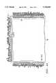
- FIG. 1is a plan view of a multi-chip module of the invention
- FIG. 2is a side view of the module of FIG. 1;
- FIG. 3is a block diagram of a multi-chip module of the invention.
- FIG. 4is a schematic representation of a multi-chip module of the invention indicating the configuration of the pins
- FIG. 5shows a PC board layout for a development board showing the mounting site for the module of FIG. 1, and
- FIG. 6is a schematic representation of a number of different modules in accordance with the invention connected to each other by means of their ISA buses to form a module family of the invention.
- Applications for such devicesinclude medical instruments, data logging devices, security systems, test equipment, point-of-sale terminals, communications devices, such as Internet and facsimile machines, and navigational instruments.
- OEMsoriginal equipment manufacturers typically use the Intel X86 architecture since it offers the world's largest body of hardware and software.
- the present inventionhas accordingly been developed to address the problems in the prior art by providing a multi-chip module packaged to resemble a large integrated circuit chip comprising a 240 pin QFP having an overall footprint of 59.54 ⁇ 79.88 min.
- the moduleincludes a set of pins constituting a bus for connection to the OEM designer's proprietary internal hardware.
- the inventionspecifically contemplates providing this bus with a configuration complying with the ISA (Industry Standard Architecture) requirements. This will allow the OEM designer quickly to incorporate IBM PC/AT hardware and software and to implement the module in ISA compatible proprietary product designs.
- FIGS. 1 and 2show a plan view and a side view, respectively, of the module.
- the module 10is a 240 pin QFP with gull wing pins having a 0.762 mm. pitch.
- the bodyis rectangular, the one side of which measures 76.2 mm and the overall footprint in this embodiment being 59.54 ⁇ 79.88 mm.
- the pinsthemselves are typically 0.5 mm wide, and the dimensions of distances 12 and 14 in FIG. 1 are 3.5 mm for this embodiment.
- trackscan be designed to lead directly from the pins to another device by making use of PC board tracks on one or both surfaces of the PC board without the need for several layers to route the various tracks. Since the pins are soldered directly to the interconnecting tracks, the system has inherent reliability in that it eliminates cables and mounting hardware that could otherwise vibrate loose. As many as half a dozen interconnecting cables, assorted connectors and mounting hardware required with many existing prior art single board computers, are thereby eliminated.
- the modulethus provides an Intel X86 compatible computer in an ultra-miniature form factor that can be integrated as easily as a semiconductor device and provides the full functionality of a desk top computer.
- Intel X86 compatible computerin an ultra-miniature form factor that can be integrated as easily as a semiconductor device and provides the full functionality of a desk top computer.
- peripheral controller modulesAs is described in greater detail below, the same concepts of using a chip-like module using a QFP package with gull wing pins and having an ISA compatible bus is extended also to peripheral controller modules.
- PC-AT ISAfull compatibility with PC-AT ISA allows for easy integration with low-cost hardware peripherals.
- ISA, compliant busmakes it easy to interface with proprietary hardware design.
- the module 10having a CPU as one of its functional circuits, is illustrated in FIG. 3 and includes the standard I/O interfaces, serial ports, a parallel port, and floppy and hard disk interfaces allowing standard hardware, cables, and software libraries to be incorporated in the design.
- the module 10includes an 80386 SX CPU 20 which is connected to a DRAM bus and an ISA bus 24 by means of core logic 26.
- the core logiccontrols AT-compatible DMA controllers, interrupt controllers, and timers/counters. It also controls the AT keyboard controller 28 and the real time clock 30.
- Two serial ports 32, 34 and a parallel port 36are provided, as are a floppy disk controller 40 and an IDE hard drive interface 42.
- internal flash memory 44is provided that is controlled by a solid state flash disk controller 46.
- Poweris controlled by means of a power monitor 48 that provides a power saving function by controlling CPU sleep modes, and by a watch dog timer 50.
- the watch dog timer 50monitors CPU cycles to detect interrupts in the cycle thereby allowing the system to be automatically reset after a predetermined time delay.
- the microprocessor and various controllers and interfacescomprise chips, preferably in die form, mounted on a multi-layer PC board, e.g. ten-layers.
- the CPU 20is a standard 33 MHz 80386 SX CPU having a DRAM controller for supporting up to 16M bytes of DRAM.
- the standard DRAM interfaceprovides all the signals for connecting standard page-mode DRAMs of various configurations, including standard 8- and 9-bit 30-pin SIMM modules and discrete components, such as standard 1M ⁇ 4 and 4M ⁇ 4 DRAM chips.
- the interfaceis designed to support 70 ns or faster DRAMs.
- the DRAM interfaceconsists of:
- serial ports 32, 34are PC-compatible asynchronous serial ports, typically treated as COM 1 and COM 2 devices by DOS.
- Either or both serial portscan be disabled using SETUP. When disabled, the port's I/O address and interrupt are made available for other expansion devices on the PC bus.
- serial portsA full complement of input and output handshaking lines are supported by the serial ports, and all serial port signals are at standard LSTTL levels.
- RS232C signal compatibilitycan be achieved by including a TTL-RS232C level converter to provide the necessary bipolar signal levels.
- the parallel portis a fully-compatible PC/AT parallel port providing bidirectional operation. It is typically used to support a line printer. As appears from the table below:
- 4.7K-ohm pull-ups (+5 V)are typically provided to the following parallel port signals:
- Parallel port registersare provided for the parallel port as appears from the table set out below:
- the DOS-compatible floppy drive interface 40allows cable connections for up to four floppy drives.
- the BIOS and DOSsupport two drives. These are configured using the BIOS SETUP function. Hardware controls for two additional drives are provided.
- the floppy drive interfacesupports the following standard floppy formats:
- Outputs to the floppy drive and from the floppy driveare "open collector". Pull-up resistors are therefore required for proper termination, both on the SMX/386 board and on one of the attached floppy drives (not both).
- the IDE hard drive interface 42is a standard interface used in PC-compatible systems for hard disk drives. Up to two drives can be connected in a master-slave arrangement. The resources are depicted in the table below:
- the IDE interface pinsare arranged to easily attach to a male PC-mounted ribbon-cable connector, the IDE drives typically being attached to the drive interface using a 40-pin ribbon cable.
- the pin configuration for the module 10 as a wholeis illustrated in FIG. 4 and is given in the pin description table below:
- the core logic 26supports a DRAM bus 22 and an ISA compatible expansion bus 24 complying in number and signal type with the IEEE-P996 requirements (and corresponding to the ISA (Industry Standard Architecture) requirements).
- the pin configuration for the expansion bus 24is given in the table below with corresponding pin numbers for expansion bus connectors A, B, C, D.
- the bus 24comprises 94 pins that includes VCC and two GND pins.
- the exact pin configuration as illustrated for the expansion bus on Page 5is a critical feature of the invention. Since it forms a single row of pins on the module 10, the pins can be easily connected directly to the expansion bus connectors without having to resort to multiple layer boards to route the PC board tracks from the module 10 to the expansion bus connectors A, B, C, D. Furthermore, as mentioned above, the present invention includes both microprocessor modules as illustrated in FIG. 3, as well as peripheral controller modules such as display controller modules, Ethernet control modules, and PCMCIA compatible modules for extended memory (RAM, ROM, EEPROM, flash memory, etc.), as well as for modem, fax, and network interfaces, and also for wireless communication devices. By providing an identical pin configuration for the ISA buses, the various modules can easily be connected to one another.
- FIG. 5illustrates a card 54 having a mounting site 56 for a module having a pin configuration as described above with reference to FIG. 4.
- the card 54provides an integrated way for system development in standard ISA passive backplane systems.
- the cardincludes an AT-bus and a PC/104 bus, and occupies a single slot in an AT-class (16-bit) passive backplane. This allows development to be performed using a terminal on a serial port as a console.
- a standard VGA or SVGA display controllercan be plugged into another slot on the backplane if desired. Instead, a PC/104 display controller can be installed directly on the PC/104 header 58 on the card 54.
- the ISA-compatible busallows an OEM to easily interface his proprietary hardware design with the module 10.
- the standard BIOS and embedded DOSallows application software to be developed using standard desk top PCs and standard development tools for implementation on the system using one or more modules of the present invention. It will be appreciated that, depending on the nature of the module, the size of the module and the number of pins may vary, however it is an important feature of this invention that the pins for the ISA bus retain their configuration in each module to allow the modules to be readily connected to one another as illustrated in FIG. 6 in which different modules 60, 62, 64 of the invention are connected to each other by means of bus lines 66, 68 extending between the ISA compatible bus pins indicated by reference numerals 70, 72, 74, respectively.
Landscapes
- Engineering & Computer Science (AREA)
- Computer Hardware Design (AREA)
- Theoretical Computer Science (AREA)
- General Physics & Mathematics (AREA)
- Microelectronics & Electronic Packaging (AREA)
- General Engineering & Computer Science (AREA)
- Physics & Mathematics (AREA)
- Condensed Matter Physics & Semiconductors (AREA)
- Power Engineering (AREA)
- Computing Systems (AREA)
- Semiconductor Integrated Circuits (AREA)
- Bus Control (AREA)
- Credit Cards Or The Like (AREA)
- Calculators And Similar Devices (AREA)
- Techniques For Improving Reliability Of Storages (AREA)
Abstract
Description
______________________________________ • Multiplexed addresses MA00-MA10 • Bidirectional data D0-D15 • Column Address Strobes CASL0- to CASL3- (low byte) CASH0- to CASH3- (high byte) • Row Address Strobes RAS0- to RAS3- • Memory Write Strobe DRWE- ______________________________________
______________________________________ Serial Typical I/O Standard Port Usage Address Interrupt ______________________________________ Serial 1 COM1 3F8-3FF IRQ4 Serial 2 COM2 2F8-2FF IRQ3 Serial Port Rersources ______________________________________
______________________________________ Parallel Typical I/O Standard Port Usage Address Interrupt ______________________________________Parallel 1 LPT1 378 IRQ7 Parallel Port Resources ______________________________________
______________________________________ Signal Active DB25F Register Bit Name In/Out High/Low Pin ______________________________________ DATA 0 PD0 I/O HIGH 2 (A+0) 1 PD1 I/O HIGH 3 2 PD2 I/O HIGH 4 3 PD3 I/O HIGH 5 4 PD4 I/O HIGH 6 5 PD5 I/O HIGH 7 6 PD6 I/O HIGH 8 7 PD7 I/O HIGH 9 STATUS 0 1 -- -- -- (A+1)) 1 1 -- -- -- 2 1 -- -- -- 3 ERROR- IN LOW 15 4 SLCT- IN HIGH 13 5 PE INHIGH 12 6 ACK-IN HIGH 10 7 BUSY IN LOW 11 CONTROL 0 STRB-OUT LOW 1 1 AUTOFD- OUT LOW 14 (A+2) 2 INIT- OUT HIGH 16 3 SLCTIN- OUT LOW 17 4 IRQ ENABLE -- HIGH -- 5 1 -- -- -- 6 1 -- -- -- 7 1 -- -- -- Parallel Port Registers ______________________________________
______________________________________ Capacity Drive Size Tracks Data Rate ______________________________________ 360K 51/4inch 40 250 KHz 1.2M 51/4 inch 80 500 KHz720K 31/2 inch 80 250 KHz 1.44M 31/2 inch 80 500 KHz ______________________________________
______________________________________ Resource Function ______________________________________ I/O Address 3F2 FDC Digital Output Register (LDOR) 3F0h-3F7h 3F4 FDC Main Status Register 3F5 FDC Data Register 3F7 FDC Control Register (LDCR) IRQ6 Interrupt DRQ2-DACK2 DMA Controller Channel Floppy Interface Resources ______________________________________
______________________________________ Floppy Pin Pin Signal Name Function In/Out ______________________________________ 11 2 DENSEL Speed/Precomp 4 N/A N/A 6 N/S Key pin N/A 12 8 INDEX- Index Pulse IN 13 10 MTR0- Motor On 0 OUT 15 12 DRV1-Drive Select 2 OUT 18 14 DRV0-Drive Select 1OUT 20 16 MTR1- Motor On 1OUT 22 18 DIR- Direction Select OUT 23 20 STEP-Step Pulse OUT 24 22 WDATA- Write Data OUT 25 24 WGATE-Write Gate OUT 26 26 TRK0- Track 0 INPUT 27 28 WRPRT- Write ProtectINPUT 28 30 RDATA- Read Data INPUT 29 32 HDSEL-Head Select OUT 30 34 DSKCHG- Disk Change INPUT 1-33 Ground Ground Floppy Drive Interface ______________________________________
______________________________________ Resource Function ______________________________________ I/O Address Hard Disk Interface 1F0h-1F7h IRQ14 Interrupt IDE Hard Disk Resources ______________________________________
______________________________________ IDE Pin Pin Signal Name Function In/Out ______________________________________ 223 1 HDRESET- Reset signal from host OUT 2 GND Ground OUT 224 3 IDED07 Data bit 7 I/O 225 4 HDD08 Data bit 8 I/O 226 5 HDD06 Data bit 6 I/O 227 6 HDD09 Data bit 9 I/O 228 7 HDD05 Data bit 5 I/O 229 8 HDD10 Data bit 10 I/O 230 9 HDD04 Data bit 4 I/O 231 10 HDD11 Data bit 11 I/O 232 11 HDD03 Data bit 3 I/O 233 12 HDD12 Data bit 12 I/O 234 13 HDD02 Data bit 2 I/O 235 14 HDD13 Data bit 13 I/O 236 15 HDD01 Data bit 1 I/O 237 18 HDD14 Data bit 14 I/O 238 17 HDD00 Data bit 0 I/O 239 18 HDD15 Data bit 15 I/O 19 GND Ground OUT 20 KEY Keyed pin N/C 21 N/A Reserved N/C 22GND Ground OUT 240 23 HDIOW- Write strobe OUT 24 GND Ground OUT 1 25 HDIOR- Read strobe OUT 26 GND Ground OUT 27 RSVD Reserved N/C 2 28 HDALE Address latch enable OUT 29 RSVD Reserved N/C 30GND Ground OUT 237 31 HDD14 Drive Interrupt request IN IDE Drive Interface ______________________________________
______________________________________ Pin Pin Name Description Type ______________________________________ 1 HDIOR- IDE I/O Read, active low. Buffered version 024 ofIOR 2 HDALE IDE Address Latch Enable, active high. 024 Buffered version ofBALE 3 IRQ14 IDE InterruptRequest 14. For use with I IDE interface. Same signal appears onpin 90. 4 IOCS16 IDE I/O Chip Select 16. A low requests a I 16-bit transfer on the SA bus. Same signal appears onpin 238. This one is used for the IDE interface. 5HDA1 IDE Address 1. Buffered version of SA1. 024 6 HDA0 IDE Address 0. Buffered version of SA0 024 7HDA2 IDE Address 2. Buffered version of SA2 024 8 HDCS- IDE Chip Select. A low indicates that data 024 is being transferred to or from the IDE drive. 9 FDCS- Floppy disk Chip Select. A low indicates 024 that data is being transferred to or from the floppy disk. 10 LEDIN LED signal from IDE drive I 11DENSEL 12 IDEX Floppy disk index pulse, input from drive I 13 MTR0- Floppy disk active lower open drain output selects motor driver 0. The motor enable bits are software controlled via the floppy's Digital Output Register (DOR). 14 MTR2- Floppy disk active low open drain output selectsmotor driver 2. The motor enable bits are software controlled via the floppy's Digital Output Register (DOR). 15 DRV1- Floppy disk active lower open drain output that selectsfloppy drive 1 16 DRV3- Floppy disk active low open drain output that selectsfloppy drive 3 17 GND 18 DRV0- Floppy disk active low open drain output that selects floppy drive 0 19 DRV2- Floppy disk active low open drain output that selectsfloppy drive 2 20 MTR1- Floppy disk active low open drain output selectsmotor driver 1. The motor enable bits are software controlled via the floppy's Digital Output Register (DOR). 21 MTR3- Floppy disk active low open drain output selectsmotor driver 3. The motor enable bits are software controlled via the floppy's Digital Output Register (DOR). 22 DIR Floppy disk open drain output that controls floppy read/write head movement direction. Low=set pin. 23 STEP Floppy disk active low output provides the step pulse to move the floppy read/write head 24 WDATA- Floppy disk active lower signal writes precompensated serial data to the selected floppy drive. This is a high open current drain output and is gated internally with WGATE-. 25 WGATE- Floppy disk active low open drain signal that enables the head to write onto the floppy disk. 26 TRK0- Floppy disk active lower Schmitt input IS indicates that the head is on track 0 of the selected drive 27 WRPRT- Floppy disk active low Schmitt input IS indicating that the disk is write protected. Any WDATA-command is ignored. 28 RDATA- Floppy disk active lower Schmitt input that IS reads raw data from the floppy disk. 29 HDSEL Floppy disk open drain output that selects the head on the selected drive. Low=side 0. 30 DSKCHG Floppy disk input signal indicating that Ihe floppy door has been opened. 315VBB 32 GND 33PF1 Powerfail 34 PF0 Powerfail 35 MR-Powerfail 36 RTCIRQ- Alarm output from the onboard real time clock 37WD0 Watchdog timer 38 SA00ISA System Address 00 024 39 OSC ISA 14.318 MHz clock. This clock is asynchronous to all other system clocks 40 SA01 ISA System Address 01 024 41 SA02 ISA System Address 02 024 42 BALE ISA Buffered Address Latch Enable 43 SA03 ISA System Address 03 024 44 SD15 ISA System Data 15 45 TC ISADMX Terminal Court 46 SA04 ISA System Address 04 024 47 MASTER-ISA 48 SD14ISA System Data 14 49 DACK2-ISA DMA 2 Acknowledgestrobe 50 SA05 ISA System Address 05 024 51 SD13 ISA System Data 13 52 IRQ3 ISA Interrupt Request 3 I 53 SA06 ISA System Address 06 024 54 DRQ7 ISA DMA 7 Request I 55 SD12ISA System Data 12 56 IRQ4 ISA Interrupt Request 4 I 57 SA07 ISA System Address 07 024 58 DACK7- ISA DMA 7 Acknowledge strobe 59 SD11 ISA System Data 11 60 IRQ5 ISA Interrupt Request 5 I 61 SA08 ISA System Address 08 024 62 DRQ6 ISA DMA 6 Request I 63 SD10ISA System Data 10 64 IRQ6OUT Floppy disk interrupt request. Normally connects to IRQ6 (pin 65) 65 IRQ6 ISA Interrupt Request 6 I 66 SA09 ISA System Address 09 024 67 GND 68 DACK6- ISA DMA 6 Acknowledge strobe 69 SD09 ISA System Data 09 70 IRQ7OUT Parallel port interrupt request, Normally connects to IRQ7 (pin 71). 71 IRQ7 ISA Interrupt Request 7 I 72 SA10 ISA System Address 10 024 73 DRQ5 ISA DMA 5 Request I 74 SD08 ISA System Data 08 75 SYSCLK ISA System Clock 76 SA11 ISA System Address 11 024 77 DACK5- ISA DMA 5 Acknowledge strobe 78 MEMW- ISA active low memory write strobe 79 REFRESH- ISA active low signal indicating current bus cycle is a memory refresh 80 SA12 ISA System Address 12 024 81 DRQ0 ISA DMA 0 Request I 82 MEMR- ISA active low memory read strobe 83 DRQ1 ISA DMA 1 Request I 84 SA13 ISA System Address 13 024 85 VCC 86 DACK0- ISA DSMA 0 Acknowledge strobe 87 LA17 ISA Latched Address 17 024 88 DACK1- ISA DMA 1 Acknowledge strobe 89 SA14 ISA System Address 14 024 90 IRQ14 ISA Interrupt Request 14, normally used I for IDE interface 91 LA18 ISA Latched address 18 024 92 DRQ3 ISA DMA 3 Request strobe 93 SA15 ISA System Address 15 024 94 IRQ15 ISA Interrupt Request 15 I 95 LA19 ISA Latched Address 19 024 96 DACK3- ISA DMA 3 Acknowledge strobe 97 SA16 ISA System Address 16 024 98 IRQ12 ISA Interrupt Request 12 I 99 LA20 ISA Latched Address 20 024 100 IOR- ISA I/O Read strobe 101 SA17 ISA System Address 17 024 102 GND 103 IRQ11 ISA Interrupt Request 11 I 104 LA21 ISA Latched Address 21 024 105 IOW- ISA I/O Write strobe 106 SA18 ISA System Address 18 024 107 IRQ10 ISA Interrupt Request 10 I 108 LA22 ISA Latched Address 22 024 109 SMEMR- ISA System Memory Read strobe 110 SA19 ISA System Address 19 024 111 IOCS16- ISA 16-bit I/O Chip Select request. I Indicates that the current I/O transaction is 16-bits. 112 LA23 ISA Latched Address 23 024 113 SMEMW- ISA System Memory Write strobe 114 AEN ISA Address Enable 115 MEMCS16 ISA 16-bit Memory Chip Select request. I Indicates that the current memory transaction is 16-bits. 116 SBHE- ISA System Byte High Enable 117 IOCHRDY ISA I/O Channel Ready. A low adds wait I states to the current ISA bus cycle 118 SD00ISA System Data 00 119 OWS- ISA active low causing cuurent memory I cycle to be controlled without additional wait states. 120 SD01 ISA System Data 01 121 SD02 ISA System Data 02 122 DRQ2OUTFloppy DMA 2 Request. Normally connected to DRDQ2 (pin 123) 123DRQ2 ISA DMA 2 Request strobe 124 SD03 ISA System Data 03 125 SD04 ISA System Data 04 126 IRQ9 ISA Interrupt Request 09 127 SD05 ISA System Data 05 128 SD06 ISA System Data 06 129 RESETDRV ISA active high systemreset signal 130 IOCHCHK ISA gated non-maskable interrupt input 131 IOCHCHK- ISA gated non-maskable interrupt input I 132 HISPEED Input to select CPU speed, High=high I speed. 133 SPKR Speaker output 134 KDATA Keyboard 135 KCLOCK Keyboard clock 136 PWRDN-137 GND 138 COLOR Video Color/Mono jumper I 139 KBLOCK Keyboard lock. Low blocks keyboard I input 140 SLCT Parallel Port 141 PE Parallel Port 142 BUSY Parallel Port 143 ACK- Parallel Port 144 PD7 Parallel Port Data 7 145 PD6 Parallel Port Data 6 146 PD5 Parallel Port Data 5 147 PD4 Parallel Port Data 4 148 PD3 Parallel Port Data 3 149 SLCTIN- Parallel Port 150 PD2 Parallel Port Data 2 151 INIT- Parallel Port 152 PD1 Parallel Port Data 1 153 ERR- Parallel Port 154 GND 155 PD0 Parallel Port Data 0 156 AUTOFD Parallel Port 157 STRB- Parallel Port 158 DCD2 Serial Port 2 Data Carrier Detect 159 DSR2 Serial Port 2 Data Set Ready 160 RXD2 Serial Port 2 Receive Data 161 RTS2 Serial Port 2 Request To Send 162 TXD2 Serial Port 2 Transmit Data 163 CTS2 Serial Port 2 Clear To Send 164 DTR2 Serial Port 2 Data Terminal Ready 165 R12 Serial Port 2 Ring Indicator 166 DCD1 Serial Port 1 Data Carrier Detect 167 DSR1 Serial Port 1 Data Set Ready 168 RXD1 Serial Port 1 Receive Data 169 RTS1 Serial Port 1 Request to Send 170 TXD1 Serial Port 1 Transmit Data 171 CTS1 Serial Port 1 Clear to Send 172 DTR1 Serial Port 1 Data Terminal Ready 173 RI1 Serial Port 1 Ring Indicator 174 GAMECS 175 RAS3- DRAM Row Address Strobe 3 176 RAS2- DRAM Row Address Strobe 2 177 RAS1- DRAM Row Address Strobe 1 178 RAS0- DRAM Row Address Strobe 0 179 DP1 DRAM parity bit for high byte memory 180 DP0 DRAM parity bit for low byte memory 181 D15 DRAM Data Bit 15 182 D07 DRAM Data Bit 7 183 D14 DRAM Data Bit 14 184 D06 DRAm Data Bit 6 185 DRWE- DRAM memory write strobe 186 D13 DRAM Data Bit 13 187 GND 188 D05 DRAM Data Bit 5 189 MA10 DRAM multiplexed memory address 10 190 MA09 DRAM multiplexed memory address 9 191 MA08 DRAM multiplexed memory address 8 192 D12 DRAM Bata Bit 12 193 D04 DRAM Data Bit 4 194 MA07 DRAM multiplexed memory address 7 195 MA06 DRAM multiplexed memory address 6 196 D11 DRAM Data Bit 11 197 D03 DRAM Data Bit 3 198 MA05 DRAM multiplexed memory address 5 199 MA04 DRAM multiplexed memory address 4 200 D10 DRAM Data Bit 10 201 D02 DRAM Data Bit 2 202 MA03 DRAM multiplexed memory address 3 203 MA02 DRAM multiplexed memory address 2 204 D09 DRAM Data Bit 9 205 VCC 206 D01 DRAM Data Bit 1 207 MA01 DRAM multiplexed memory address 1 208 MA00 DRAM multiplexed memory address 0 209 D08 DRAM Data Bit 8 210 D00 DRAM Data Bit 0 211 CASH3- DRAM Column Address Strobe, High byte 3 212 CASL3- DRAM Column Address Strobe, Low byte 3 213 CASH2- DRAM Column Address Strobe, High byte 2 214 CASL2- DRAM Column Address Strobe, Low byte 2 215 CASH1- DRAM Column Address Strobe, High byte 1 216 CASL1- DRAM Column Address Strobe, Low byte 1 217 CASH0- DRAM Column Address Strobe, High byte 0 218 CASL0- DRAM Column Address Strobe, Low byte 0 219 BDIS 220 XROMCS- 221 LEDOUT- 222 GND 223 HDRESET- IDE 224 IDE07 IDE Data Bit 7 225 HDD08 IDE Data Bit 8 226 HDD06 IDE Data Bit 6 227 HDD09 IDE Data Bit 9 228 HDD05 IDE Data Bit 5 229 HDD10 IDE Data Bit 10 230 HDD04 IDE Data Bit 4 231 HDD11 IDE Data Bit 11 232 HDD03 IDE Data Bit 3 233 HDD12 IDE Data Bit 12 234 HDD02 IDE Data Bit 2 235 HDD13 IDE Data Bit 13 236 HDD01 IDE Data Bit 1 237 HDD14 IDE Data Bit 14 238 HDD00 IDE Data Bit 0 239 HDD15 IDE Data Bit 15 240 HDIOW- IDE buffered I/O Write strobe ______________________________________
__________________________________________________________________________ Signal Pin Name Function In/Out Current Load* __________________________________________________________________________38 A31 SA0 Address bit 0 I/O 12 mA PU 39 B30 OSC 14.318 MHz clock Out 6 mA 33 SER 40 A30 SA1 Address bit 1 I/O 12 mA PU 41 A29 SA2 Address bit 2 I/O 12 mA PU 42 B28 BALE Address latch Out 12 mA enable 43 A28 SA3 Address bit 3 I/O 12 mA PU 44 C18 SD15 System Data bit I/O 12 mA PU 15 45 B27 TC DMA Terminal Out 4 mA Count 46 A27 SA4 Address bit 4 I/O 12 mA PU 47 D17 MASTER- Bus master assert In N/A 330 PU 48 C17 SD14 System Data bit I/O 24 mA PU 14 49 B26 DACK2- DMA Out 4 mA Acknowledge 2 50 A26 SA5 Address bit 5 I/O 12 mA PU 51 C16 SD13 System Data bit I/O 24 mA PU 13 52 B25 IRQ3 Interrupt Request 3 In N/A PU 53 A25 SA6 Address bit 6 I/O 12 mA PU 54 D15 DRQ7 DMA Request 7 In N/A PD 55 C15 SD12 System Data bit I/O 24 mA PU 12 56 B24 IRQ4 Interrupot Request 4 In N/A PU 57 A24 SA7 Address bit 7 I/O 12 mA PU 58 D14 DACK7- DMA Out 4 mA Acknowledge 7 59 C14 SD11 System Data bit I/O 24 mA PU 11 60 B23 IRQ5 Interrupt Request 5 In N/A PU 61 A23 SA8 Address bit 8 I/O 12 mA PU 62 D13 DRQ6 DMA Request 6 In N/A PD 63 C13 SD10 System Data bit I/O 24 mA PU 10 64 IRQ6OUT Floppy Disk Interrupt Request 65 B22 IRQ6 Interrupt Request 6 In N/A PU 66 A22 SA9 Address bit 9 I/O 12 mA PU 67 GND 68 D12 DACK6- DMA Out 4 mA Acknowledge 6 69 C12 SD9 System Data bit 9 I/O 24 mA PU 70 IRQ7OUT Parallel Port Interrupt Request 71 821 IRQ7 Interrupt Request 7 In N/A PU 72 A21 SA10 Address bit 10 I/O 12 mA PU 73 D11 DRQ5 DMA Request 5 In N/A PD 74 C11 SD8 System Data bit 8 I/O 24 mA PU 75 B20 SYSCLK System clock (8 Out 12 mA MHz) 76 A20 SA11 Address bit 11 I/O 12 mA PU 77 D10 DACK5- DMA Out 4 mA Acknowledge 5 78 C10 MEMW- Memory Write I/O 6 mA PU, 33 SER 79 B19 REFRESH- Memory Refresh I/O 6 mA 470 PU, 33 SER 80 A19 SA12 Address bit 12 I/O 12 mA PU 81 D9 DRQ0 DMA Request 9 In N/A PD 82 C9 MEMR- Memory Read I/O 6 mA PU, 33 SER 83 B18 DRQ1 DMA Request 1 In N/A PD 84 A18 SAT3 Address bit 13 I/O 12 mA PU 85 VCC 86 D8 DACK0- DMA Out 4 mA Acknowledge 0 87 C8 LA17 Address bit 17 I/O 24 mA 88 B17 DACK1- DMA Out 4 mA Acknowledge 1 89 A17 SA14 Address bit 14 I/O 12 mA PU 90 D7 IRQ14 Interrupt Request In N/A PU 14 91 C7 LA18 Address bit 18 I/O 24 mA 92 B16 DRQ3 DMA Request 3 In N/A PD 93 A16 SA15 Address bit 15 I/O 12 mA PU 94 D6 IRQ15 Interrupt Request In N/A PU 15 95 C6 LA19 Address bit 19 I/O 24 mA 96 B15 DACK3- DMA Out 4 mA Acknowledge 3 97 A15 SA16 Address bit 16 I/O 12 mA PU 98 D5 IRQ12 Interrupt Request In N/A PU 12 99 C5 LA20 Address bit 20 I/O 24 mA 100 B14 IRQ- I/O Read I/O 6 mA PU 101 A14 SA17 Address bit 17 I/O 12 mA PU 102 GND 103 D4 IRQ11 Interrupt Request In N/A PU 11 104 C4 LA21 Address bit 21 I/O 24 mA 105 B13 IOW- I/O Write I/O 6 mA PU 106 A13 SA18 Address bit 18 I/O 12 mA PU 107 D3 IRQ10 Interrupt Request In N/A PU 10 108 C3 LA22 Address bit 22 I/O 24 mA 109 B12 SMEMR- Mem Read (lower I/O 6 mA 33 SER 1MB) 110 A12 SA19 Address bit 19 I/O 12 mA PU 111 D2 IOCS16- 16-bit I/O access In N/A 330 PU 112 C2 LA23 Address bit 23 I/O 24 mA 113 B11 SMEMW- Mem Write (lower I/O 6 mA 33 SER 1 MB) 114 A11 AEN Address Enable I/O 12 mA PU 115 D1 MEMCS16- 16-bit mem access In N/A 330 PU 116 C1 SBHE- Bus High Enable I/O 12 mA PU 117 A10 IOCHRDY Processor Ready In N/A 1K PU Ctrl 118 A9 SD00 System Data bit 0 I/O 24 mA PU 119 B8 ENDXFR- Zero wait state In N/A 330 PU (OWS-) 120 A8 SD1 System Data bit 1 I/O 24 mA PU 121 A7 SD2 System Data bit 2 I/O 24 mA PU 122 DRQ2OUT Floppy DMA 2 Request 123 B6 DRQ2 DMA Request 2 In N/A PD 124 A6 SD3 System Data bit 3 I/O 24 mA PU 125 A5 SD4 System Data bit 4 I/O 24 mA PU 126 B4 IRQ9 Interrupt request 9 In N/A PU 127 A4 SD5 System Data bit 5 I/O 24 mA PU 128 A4 SD6 System Data bit 6 I/O 24 mA PU 129 B2 RESETDRV System reset Out 24 mA signal 130 A2 SD7 System Data bit 7 I/O 24 mA PU 131 A1 IOCHCK- Sub NMI input In N/A 4.7K PU __________________________________________________________________________
Claims (2)
Priority Applications (12)
| Application Number | Priority Date | Filing Date | Title |
|---|---|---|---|
| US08/564,688US5742844A (en) | 1995-11-29 | 1995-11-29 | IBM PC compatible multi-chip module |
| PCT/US1996/019064WO1997020273A1 (en) | 1995-11-29 | 1996-11-27 | Ibm pc compatible multi-chip module |
| DE29623495UDE29623495U1 (en) | 1995-11-29 | 1996-11-27 | IBM PC compatible multi-chip module |
| JP9520690AJPH11508713A (en) | 1995-11-29 | 1996-11-27 | Multiple chip type module compatible with IBM personal computer |
| EP96942093AEP0864127A4 (en) | 1995-11-29 | 1996-11-27 | Ibm pc compatible multi-chip module |
| CH01218/98ACH690527A5 (en) | 1995-11-29 | 1996-11-27 | IMB PC compatible multi-chip module. |
| GB9811497AGB2322462B (en) | 1995-11-29 | 1996-11-27 | IBM PC Compatible multi-chip module |
| AU11256/97AAU1125697A (en) | 1995-11-29 | 1996-11-27 | Ibm pc compatible multi-chip module |
| CA002232894ACA2232894C (en) | 1995-11-29 | 1996-11-27 | Ibm pc compatible multi-chip module |
| US08/757,896US6101593A (en) | 1995-11-29 | 1996-11-27 | IBM PC compatible multi-chip module |
| US09/008,553US6038663A (en) | 1995-11-29 | 1998-01-16 | IBM PC compatible multi-chip module |
| US09/524,858US6711666B1 (en) | 1995-11-29 | 2000-03-14 | IBM PC compatible multi-chip module |
Applications Claiming Priority (1)
| Application Number | Priority Date | Filing Date | Title |
|---|---|---|---|
| US08/564,688US5742844A (en) | 1995-11-29 | 1995-11-29 | IBM PC compatible multi-chip module |
Related Child Applications (1)
| Application Number | Title | Priority Date | Filing Date |
|---|---|---|---|
| US08/757,896Continuation-In-PartUS6101593A (en) | 1995-11-29 | 1996-11-27 | IBM PC compatible multi-chip module |
Publications (1)
| Publication Number | Publication Date |
|---|---|
| US5742844Atrue US5742844A (en) | 1998-04-21 |
Family
ID=24255479
Family Applications (3)
| Application Number | Title | Priority Date | Filing Date |
|---|---|---|---|
| US08/564,688Expired - LifetimeUS5742844A (en) | 1995-11-29 | 1995-11-29 | IBM PC compatible multi-chip module |
| US08/757,896Expired - LifetimeUS6101593A (en) | 1995-11-29 | 1996-11-27 | IBM PC compatible multi-chip module |
| US09/008,553Expired - LifetimeUS6038663A (en) | 1995-11-29 | 1998-01-16 | IBM PC compatible multi-chip module |
Family Applications After (2)
| Application Number | Title | Priority Date | Filing Date |
|---|---|---|---|
| US08/757,896Expired - LifetimeUS6101593A (en) | 1995-11-29 | 1996-11-27 | IBM PC compatible multi-chip module |
| US09/008,553Expired - LifetimeUS6038663A (en) | 1995-11-29 | 1998-01-16 | IBM PC compatible multi-chip module |
Country Status (9)
| Country | Link |
|---|---|
| US (3) | US5742844A (en) |
| EP (1) | EP0864127A4 (en) |
| JP (1) | JPH11508713A (en) |
| AU (1) | AU1125697A (en) |
| CA (1) | CA2232894C (en) |
| CH (1) | CH690527A5 (en) |
| DE (1) | DE29623495U1 (en) |
| GB (1) | GB2322462B (en) |
| WO (1) | WO1997020273A1 (en) |
Cited By (16)
| Publication number | Priority date | Publication date | Assignee | Title |
|---|---|---|---|---|
| US5909587A (en)* | 1997-10-24 | 1999-06-01 | Advanced Micro Devices, Inc. | Multi-chip superscalar microprocessor module |
| US5951666A (en)* | 1996-11-28 | 1999-09-14 | Lucent Technologies Inc. | Bus system having both serial and parallel busses |
| US6038663A (en)* | 1995-11-29 | 2000-03-14 | Zf Microsystems, Inc. | IBM PC compatible multi-chip module |
| US6154789A (en)* | 1998-06-15 | 2000-11-28 | Compaq Computer Corporation | Peripheral controller comprising first messaging unit for communication with first OS driver and second messaging unit for communication with second OS driver for mass-storage peripheral |
| US6520809B1 (en) | 1997-09-03 | 2003-02-18 | Samsung Electronics Co., Ltd. | Power pins in hard disk drive |
| US20030135687A1 (en)* | 2002-01-15 | 2003-07-17 | Owens Brian Keith | Memory module, printer assembly, and method for storing printer code |
| US6721817B1 (en)* | 1997-01-21 | 2004-04-13 | Dell Usa, L.P. | Original equipment manufacturer identification for configurable electronic hardware |
| US6784372B1 (en)* | 2000-05-26 | 2004-08-31 | Albert T. Yuen | Orthogonal electrical connection using a ball edge array |
| US20050057907A1 (en)* | 2003-09-12 | 2005-03-17 | Hewlett-Packard Development Company, L.P. | Circuit board assembly |
| US20050073817A1 (en)* | 2003-10-07 | 2005-04-07 | Hewlett-Packard Development Company, L.P. | Circuit board assembly |
| US20050073813A1 (en)* | 2003-10-07 | 2005-04-07 | Hewlett-Packard Development Company, L.P. | Circuit board assembly |
| US7056144B2 (en) | 2004-02-19 | 2006-06-06 | Hewlett-Packard Development Company, L.P. | Offset compensation system |
| US20070126101A1 (en)* | 2005-12-05 | 2007-06-07 | A-Data Technology Co., Ltd. | Memory card module |
| US20080080150A1 (en)* | 2006-09-29 | 2008-04-03 | Hewlett-Packard Development Company Lp | Sequencer |
| US20080101031A1 (en)* | 2006-10-25 | 2008-05-01 | Hewlett-Packard Development Company Lp | Wedge lock |
| US10055000B2 (en) | 2014-11-12 | 2018-08-21 | Alibaba Group Holding Limited | Method and apparatus for controlling hard drive power consumption and controlling a management service of hard drive power consumption |
Families Citing this family (23)
| Publication number | Priority date | Publication date | Assignee | Title |
|---|---|---|---|---|
| DE19912441A1 (en)* | 1999-03-19 | 2000-09-21 | Elfo Ag Sachseln Sachseln | Multi-chip module |
| US6571347B1 (en)* | 1999-05-24 | 2003-05-27 | Winbond Electronics Corporation | Apparatus and method for intelligent computer initiation program recovery |
| TW462025B (en)* | 1999-06-23 | 2001-11-01 | Micro Star Int Co Ltd | BIOS virus protection method |
| WO2001024014A1 (en)* | 1999-09-27 | 2001-04-05 | Zf Micro Devices, Inc. | Embedded computer system and method with flash memory interface |
| US7231513B1 (en)* | 1999-12-17 | 2007-06-12 | Intel Corporation | Dynamically linked basic input/output system |
| US6738879B2 (en)* | 2000-05-22 | 2004-05-18 | Seagate Technology Llc | Advanced technology attachment compatible disc drive write protection scheme |
| US6757838B1 (en)* | 2000-10-13 | 2004-06-29 | Hewlett-Packard Development Company, L.P. | Hardware independent implementation of computer system BIOS recovery |
| US7266731B2 (en)* | 2001-11-13 | 2007-09-04 | Sun Microsystems, Inc. | Method and apparatus for managing remote software code update |
| KR100429265B1 (en)* | 2001-11-14 | 2004-04-29 | 엘지전자 주식회사 | Common communication interface by programable logic divice |
| ES2327510T3 (en)* | 2002-02-25 | 2009-10-30 | Scott Laboratories, Inc. | PROTECTION MODULE AGAINST FAILURES, INTEGRATED WITH AN ANALGESY AND SEDATION SYSTEM. |
| US6934873B2 (en)* | 2002-02-28 | 2005-08-23 | Dell Products L.P. | Automatic BIOS recovery in a multi-node computer system |
| TW571240B (en)* | 2002-07-10 | 2004-01-11 | Akom Technology Inc | Display method for debugging code of BISO |
| JP3960169B2 (en)* | 2002-08-30 | 2007-08-15 | 富士通株式会社 | Information processing apparatus and recovery method therefor |
| TW584800B (en)* | 2002-10-25 | 2004-04-21 | Via Tech Inc | Method, computer and peripheral/expansion bus bridge for booting up with debug system |
| TWI221959B (en)* | 2002-10-25 | 2004-10-11 | Via Tech Inc | Method and computer system using a debug system to boot up |
| US20050081090A1 (en)* | 2003-09-29 | 2005-04-14 | Giga-Byte Technology Co., Ltd. | Method for automatically and safely recovering BIOS memory circuit in memory device including double BIOS memory circuits |
| CN100530146C (en)* | 2004-08-26 | 2009-08-19 | 鸿富锦精密工业(深圳)有限公司 | BIOS on-line rewriting method |
| CN100369224C (en)* | 2005-05-08 | 2008-02-13 | 薛萍 | Chip with built-in software and hardware system and making method thereof |
| US9214431B1 (en)* | 2006-05-25 | 2015-12-15 | Qualcomm Incorporated | On-chip/off-chip magnetic shielding loop |
| CN103164353A (en)* | 2011-12-12 | 2013-06-19 | 鸿富锦精密工业(深圳)有限公司 | Recognition circuit |
| CN102970027B (en)* | 2012-11-27 | 2015-05-13 | 杭州电子科技大学 | Level switch and serial port transceiver circuit |
| SE1650648A1 (en)* | 2016-05-13 | 2017-11-07 | Oniteo Ab | Method and system for fail-safe booting |
| CN106339238B (en)* | 2016-08-26 | 2020-03-24 | 卢军 | Serial port multi-mode automatic multiplexing chip fast programming system |
Family Cites Families (5)
| Publication number | Priority date | Publication date | Assignee | Title |
|---|---|---|---|---|
| US4763188A (en)* | 1986-08-08 | 1988-08-09 | Thomas Johnson | Packaging system for multiple semiconductor devices |
| DE19513275A1 (en)* | 1994-06-27 | 1996-01-11 | Hewlett Packard Co | Probe adaptor for connecting integrated circuit components to electronic test-measurement appts. |
| US5659680A (en)* | 1995-06-30 | 1997-08-19 | Micro Processor Systems, Inc. | PC compatible modular based diagnostic system |
| US5742844A (en)* | 1995-11-29 | 1998-04-21 | Zf Microsystems, Inc. | IBM PC compatible multi-chip module |
| US5793943A (en)* | 1996-07-29 | 1998-08-11 | Micron Electronics, Inc. | System for a primary BIOS ROM recovery in a dual BIOS ROM computer system |
- 1995
- 1995-11-29USUS08/564,688patent/US5742844A/ennot_activeExpired - Lifetime
- 1996
- 1996-11-27CACA002232894Apatent/CA2232894C/ennot_activeExpired - Fee Related
- 1996-11-27USUS08/757,896patent/US6101593A/ennot_activeExpired - Lifetime
- 1996-11-27AUAU11256/97Apatent/AU1125697A/ennot_activeAbandoned
- 1996-11-27GBGB9811497Apatent/GB2322462B/ennot_activeExpired - Fee Related
- 1996-11-27EPEP96942093Apatent/EP0864127A4/ennot_activeWithdrawn
- 1996-11-27DEDE29623495Upatent/DE29623495U1/ennot_activeExpired - Lifetime
- 1996-11-27CHCH01218/98Apatent/CH690527A5/ennot_activeIP Right Cessation
- 1996-11-27JPJP9520690Apatent/JPH11508713A/enactivePending
- 1996-11-27WOPCT/US1996/019064patent/WO1997020273A1/ennot_activeApplication Discontinuation
- 1998
- 1998-01-16USUS09/008,553patent/US6038663A/ennot_activeExpired - Lifetime
Non-Patent Citations (11)
| Title |
|---|
| "Personal Computer Bus Standard P 1996," IEEE, 1991, pp. i-xiv and 1.1 to A.17. |
| Advance Information re NorthStar III 100 and III 90, MicroModule Systems, 1 11.* |
| Advance Information re NorthStar III-100 and III-90, MicroModule Systems, 1-11. |
| Data Sheet, S MOS Systems, (1994).* |
| Data Sheet, S-MOS Systems, (1994). |
| Intel 386 SL . . . Superset, System design Guide, 1992, pp. 1 1 to 2 13, 7 1 to 7 25 and D 4, 1992.* |
| Intel 386 SL . . . Superset, System design Guide, 1992, pp. 1-1 to 2-13, 7-1 to 7-25 and D-4, 1992. |
| Intel 486SL . . . Superset, System design Guide, 1992, pp. 1 1 to 2 11 and 5 1 to 5 24, 1992.* |
| Intel 486SL . . . Superset, System design Guide, 1992, pp. 1-1 to 2-11 and 5-1 to 5-24, 1992. |
| MicroModlue Adds to Northstar, CMP Publications, (Mar. 27, 1995).* |
| Personal Computer Bus Standard P 1996, IEEE, 1991, pp. i xiv and 1.1 to A.17.* |
Cited By (24)
| Publication number | Priority date | Publication date | Assignee | Title |
|---|---|---|---|---|
| US6038663A (en)* | 1995-11-29 | 2000-03-14 | Zf Microsystems, Inc. | IBM PC compatible multi-chip module |
| US6101593A (en)* | 1995-11-29 | 2000-08-08 | Zf Linux Devices, Inc. | IBM PC compatible multi-chip module |
| US5951666A (en)* | 1996-11-28 | 1999-09-14 | Lucent Technologies Inc. | Bus system having both serial and parallel busses |
| US6721817B1 (en)* | 1997-01-21 | 2004-04-13 | Dell Usa, L.P. | Original equipment manufacturer identification for configurable electronic hardware |
| US6520809B1 (en) | 1997-09-03 | 2003-02-18 | Samsung Electronics Co., Ltd. | Power pins in hard disk drive |
| US5909587A (en)* | 1997-10-24 | 1999-06-01 | Advanced Micro Devices, Inc. | Multi-chip superscalar microprocessor module |
| US6154789A (en)* | 1998-06-15 | 2000-11-28 | Compaq Computer Corporation | Peripheral controller comprising first messaging unit for communication with first OS driver and second messaging unit for communication with second OS driver for mass-storage peripheral |
| US6784372B1 (en)* | 2000-05-26 | 2004-08-31 | Albert T. Yuen | Orthogonal electrical connection using a ball edge array |
| US20030135687A1 (en)* | 2002-01-15 | 2003-07-17 | Owens Brian Keith | Memory module, printer assembly, and method for storing printer code |
| US7209252B2 (en) | 2002-01-15 | 2007-04-24 | Lexmark International, Inc. | Memory module, printer assembly, and method for storing printer code |
| US20050057907A1 (en)* | 2003-09-12 | 2005-03-17 | Hewlett-Packard Development Company, L.P. | Circuit board assembly |
| US20050073817A1 (en)* | 2003-10-07 | 2005-04-07 | Hewlett-Packard Development Company, L.P. | Circuit board assembly |
| US20050073813A1 (en)* | 2003-10-07 | 2005-04-07 | Hewlett-Packard Development Company, L.P. | Circuit board assembly |
| US7345891B2 (en) | 2003-10-07 | 2008-03-18 | Hewlett-Packard Development Company, L.P. | Circuit board assembly |
| US7061126B2 (en) | 2003-10-07 | 2006-06-13 | Hewlett-Packard Development Company, L.P. | Circuit board assembly |
| US7646595B2 (en) | 2003-10-07 | 2010-01-12 | Hewlett-Packard Development Company, L.P. | Computing device |
| US7056144B2 (en) | 2004-02-19 | 2006-06-06 | Hewlett-Packard Development Company, L.P. | Offset compensation system |
| US7420830B2 (en)* | 2005-12-05 | 2008-09-02 | A-Data Technology Co., Ltd. | Memory card module |
| US20070126101A1 (en)* | 2005-12-05 | 2007-06-07 | A-Data Technology Co., Ltd. | Memory card module |
| US20080080150A1 (en)* | 2006-09-29 | 2008-04-03 | Hewlett-Packard Development Company Lp | Sequencer |
| US7742310B2 (en) | 2006-09-29 | 2010-06-22 | Hewlett-Packard Development Company, L.P. | Sequencer |
| US20080101031A1 (en)* | 2006-10-25 | 2008-05-01 | Hewlett-Packard Development Company Lp | Wedge lock |
| US7397666B2 (en) | 2006-10-25 | 2008-07-08 | Hewlett-Packard Development Company, L.P. | Wedge lock |
| US10055000B2 (en) | 2014-11-12 | 2018-08-21 | Alibaba Group Holding Limited | Method and apparatus for controlling hard drive power consumption and controlling a management service of hard drive power consumption |
Also Published As
| Publication number | Publication date |
|---|---|
| CH690527A5 (en) | 2000-09-29 |
| EP0864127A4 (en) | 1999-01-27 |
| WO1997020273A1 (en) | 1997-06-05 |
| US6038663A (en) | 2000-03-14 |
| EP0864127A1 (en) | 1998-09-16 |
| US6101593A (en) | 2000-08-08 |
| DE29623495U1 (en) | 1998-08-20 |
| GB9811497D0 (en) | 1998-07-29 |
| AU1125697A (en) | 1997-06-19 |
| GB2322462A (en) | 1998-08-26 |
| CA2232894A1 (en) | 1997-06-05 |
| CA2232894C (en) | 2000-02-01 |
| JPH11508713A (en) | 1999-07-27 |
| GB2322462B (en) | 1999-09-22 |
Similar Documents
| Publication | Publication Date | Title |
|---|---|---|
| US5742844A (en) | IBM PC compatible multi-chip module | |
| US5083259A (en) | Computer bus interconnection device | |
| US6003100A (en) | User-removable central processing unit card for an electrical device | |
| US20020103988A1 (en) | Microprocessor with integrated interfaces to system memory and multiplexed input/output bus | |
| US5557757A (en) | High performance integrated processor architecture including a sub-bus control unit for generating signals to control a secondary, non-multiplexed external bus | |
| US5555381A (en) | Microcomputer architecture utilizing an asynchronous bus between microprocessor and industry standard synchronous bus | |
| EP1688847B1 (en) | Die-to-die interconnect interface and protocol for stacked semiconductor dies | |
| US5280590A (en) | Logic support chip for AT-type computer with improved bus architecture | |
| US5819096A (en) | PCI to ISA interrupt protocol converter and selection mechanism | |
| JP3609466B2 (en) | Computer system | |
| US5265237A (en) | Byte swapping apparatus for selectively reordering bytes of an N-bit word communicated between an at computer and VME bus | |
| US5384692A (en) | Socket with in-socket embedded integrated circuit | |
| US5561772A (en) | Expansion bus system for replicating an internal bus as an external bus with logical interrupts replacing physical interrupt lines | |
| EP0884715A1 (en) | Single-chip chipset with integrated graphics controller | |
| EP0423036A2 (en) | CPU-bus controller | |
| KR20010032060A (en) | Interface optimized computer system architecture | |
| JPH07262131A (en) | Integrated circuit and computer upgrade method | |
| EP0658852A3 (en) | Computer system with derived local bus | |
| US6711666B1 (en) | IBM PC compatible multi-chip module | |
| US5859649A (en) | Data processing system having display controller with bursting direct memory access | |
| JPH0673363B2 (en) | System LSI design method | |
| US20020003746A1 (en) | Memory address driver circuit | |
| US5812801A (en) | Apparatus and method for implementing an alternate bus standard in a computer system not designed for the alternate bus standard | |
| EP0472274A1 (en) | Data processing apparatus having connectors to receive system components | |
| JP2001290754A (en) | Computer system |
Legal Events
| Date | Code | Title | Description |
|---|---|---|---|
| AS | Assignment | Owner name:ZF MICROSYSTEMS, INC., CALIFORNIA Free format text:ASSIGNMENT OF ASSIGNORS INTEREST;ASSIGNOR:FELDMAN, DAVID L.;REEL/FRAME:007825/0336 Effective date:19951128 | |
| STCF | Information on status: patent grant | Free format text:PATENTED CASE | |
| AS | Assignment | Owner name:ZF EMBEDDED, INC., CALIFORNIA Free format text:CHANGE OF NAME;ASSIGNOR:ZF MICROSYSTEMS, INC.;REEL/FRAME:010327/0561 Effective date:19990729 | |
| AS | Assignment | Owner name:ZF LINUX DEVICES, INC., CALIFORNIA Free format text:CHANGE OF NAME;ASSIGNOR:ZF EMBEDDED, INC.;REEL/FRAME:010814/0214 Effective date:20000211 | |
| AS | Assignment | Owner name:ZF MICRO DEVICES, INC., CALIFORNIA Free format text:CHANGE OF NAME;ASSIGNOR:ZF LINUX DEVICES, INC.;REEL/FRAME:011751/0896 Effective date:20010302 | |
| FPAY | Fee payment | Year of fee payment:4 | |
| AS | Assignment | Owner name:ZF MICRO SOLUTIONS, INC., CALIFORNIA Free format text:ASSIGNMENT OF ASSIGNORS INTEREST;ASSIGNOR:ZF MICRO DEVICES, INC.;REEL/FRAME:013663/0649 Effective date:20021206 | |
| FEPP | Fee payment procedure | Free format text:PAYOR NUMBER ASSIGNED (ORIGINAL EVENT CODE: ASPN); ENTITY STATUS OF PATENT OWNER: SMALL ENTITY | |
| FPAY | Fee payment | Year of fee payment:8 | |
| FPAY | Fee payment | Year of fee payment:12 |