US5742595A - Processing CDMA signals - Google Patents
Processing CDMA signalsDownload PDFInfo
- Publication number
- US5742595A US5742595AUS08/558,675US55867595AUS5742595AUS 5742595 AUS5742595 AUS 5742595AUS 55867595 AUS55867595 AUS 55867595AUS 5742595 AUS5742595 AUS 5742595A
- Authority
- US
- United States
- Prior art keywords
- signal
- value
- power
- signals
- summed signal
- Prior art date
- Legal status (The legal status is an assumption and is not a legal conclusion. Google has not performed a legal analysis and makes no representation as to the accuracy of the status listed.)
- Expired - Lifetime
Links
Images


Classifications
- H—ELECTRICITY
- H04—ELECTRIC COMMUNICATION TECHNIQUE
- H04Q—SELECTING
- H04Q11/00—Selecting arrangements for multiplex systems
- H04Q11/04—Selecting arrangements for multiplex systems for time-division multiplexing
- G—PHYSICS
- G06—COMPUTING OR CALCULATING; COUNTING
- G06F—ELECTRIC DIGITAL DATA PROCESSING
- G06F9/00—Arrangements for program control, e.g. control units
- G06F9/06—Arrangements for program control, e.g. control units using stored programs, i.e. using an internal store of processing equipment to receive or retain programs
- G06F9/46—Multiprogramming arrangements
- G06F9/54—Interprogram communication
- G06F9/546—Message passing systems or structures, e.g. queues
- H—ELECTRICITY
- H04—ELECTRIC COMMUNICATION TECHNIQUE
- H04B—TRANSMISSION
- H04B1/00—Details of transmission systems, not covered by a single one of groups H04B3/00 - H04B13/00; Details of transmission systems not characterised by the medium used for transmission
- H04B1/69—Spread spectrum techniques
- H04B1/707—Spread spectrum techniques using direct sequence modulation
- H04B1/7073—Synchronisation aspects
- H04B1/7075—Synchronisation aspects with code phase acquisition
- H04B1/7077—Multi-step acquisition, e.g. multi-dwell, coarse-fine or validation
- H—ELECTRICITY
- H04—ELECTRIC COMMUNICATION TECHNIQUE
- H04B—TRANSMISSION
- H04B1/00—Details of transmission systems, not covered by a single one of groups H04B3/00 - H04B13/00; Details of transmission systems not characterised by the medium used for transmission
- H04B1/69—Spread spectrum techniques
- H04B1/707—Spread spectrum techniques using direct sequence modulation
- H04B1/7073—Synchronisation aspects
- H04B1/7085—Synchronisation aspects using a code tracking loop, e.g. a delay-locked loop
- H—ELECTRICITY
- H04—ELECTRIC COMMUNICATION TECHNIQUE
- H04J—MULTIPLEX COMMUNICATION
- H04J13/00—Code division multiplex systems
- H—ELECTRICITY
- H04—ELECTRIC COMMUNICATION TECHNIQUE
- H04J—MULTIPLEX COMMUNICATION
- H04J3/00—Time-division multiplex systems
- H04J3/02—Details
- H04J3/06—Synchronising arrangements
- H04J3/0635—Clock or time synchronisation in a network
- H04J3/0682—Clock or time synchronisation in a network by delay compensation, e.g. by compensation of propagation delay or variations thereof, by ranging
- H—ELECTRICITY
- H04—ELECTRIC COMMUNICATION TECHNIQUE
- H04L—TRANSMISSION OF DIGITAL INFORMATION, e.g. TELEGRAPHIC COMMUNICATION
- H04L12/00—Data switching networks
- H04L12/66—Arrangements for connecting between networks having differing types of switching systems, e.g. gateways
- H—ELECTRICITY
- H04—ELECTRIC COMMUNICATION TECHNIQUE
- H04L—TRANSMISSION OF DIGITAL INFORMATION, e.g. TELEGRAPHIC COMMUNICATION
- H04L41/00—Arrangements for maintenance, administration or management of data switching networks, e.g. of packet switching networks
- H04L41/02—Standardisation; Integration
- H04L41/0226—Mapping or translating multiple network management protocols
- H—ELECTRICITY
- H04—ELECTRIC COMMUNICATION TECHNIQUE
- H04L—TRANSMISSION OF DIGITAL INFORMATION, e.g. TELEGRAPHIC COMMUNICATION
- H04L41/00—Arrangements for maintenance, administration or management of data switching networks, e.g. of packet switching networks
- H04L41/02—Standardisation; Integration
- H04L41/0233—Object-oriented techniques, for representation of network management data, e.g. common object request broker architecture [CORBA]
- H—ELECTRICITY
- H04—ELECTRIC COMMUNICATION TECHNIQUE
- H04L—TRANSMISSION OF DIGITAL INFORMATION, e.g. TELEGRAPHIC COMMUNICATION
- H04L41/00—Arrangements for maintenance, administration or management of data switching networks, e.g. of packet switching networks
- H04L41/08—Configuration management of networks or network elements
- H—ELECTRICITY
- H04—ELECTRIC COMMUNICATION TECHNIQUE
- H04L—TRANSMISSION OF DIGITAL INFORMATION, e.g. TELEGRAPHIC COMMUNICATION
- H04L41/00—Arrangements for maintenance, administration or management of data switching networks, e.g. of packet switching networks
- H04L41/22—Arrangements for maintenance, administration or management of data switching networks, e.g. of packet switching networks comprising specially adapted graphical user interfaces [GUI]
- H—ELECTRICITY
- H04—ELECTRIC COMMUNICATION TECHNIQUE
- H04L—TRANSMISSION OF DIGITAL INFORMATION, e.g. TELEGRAPHIC COMMUNICATION
- H04L43/00—Arrangements for monitoring or testing data switching networks
- H—ELECTRICITY
- H04—ELECTRIC COMMUNICATION TECHNIQUE
- H04L—TRANSMISSION OF DIGITAL INFORMATION, e.g. TELEGRAPHIC COMMUNICATION
- H04L69/00—Network arrangements, protocols or services independent of the application payload and not provided for in the other groups of this subclass
- H04L69/14—Multichannel or multilink protocols
- H—ELECTRICITY
- H04—ELECTRIC COMMUNICATION TECHNIQUE
- H04W—WIRELESS COMMUNICATION NETWORKS
- H04W52/00—Power management, e.g. Transmission Power Control [TPC] or power classes
- H04W52/04—Transmission power control [TPC]
- H—ELECTRICITY
- H04—ELECTRIC COMMUNICATION TECHNIQUE
- H04W—WIRELESS COMMUNICATION NETWORKS
- H04W52/00—Power management, e.g. Transmission Power Control [TPC] or power classes
- H04W52/04—Transmission power control [TPC]
- H04W52/52—Transmission power control [TPC] using AGC [Automatic Gain Control] circuits or amplifiers
- H—ELECTRICITY
- H04—ELECTRIC COMMUNICATION TECHNIQUE
- H04B—TRANSMISSION
- H04B1/00—Details of transmission systems, not covered by a single one of groups H04B3/00 - H04B13/00; Details of transmission systems not characterised by the medium used for transmission
- H04B1/69—Spread spectrum techniques
- H04B1/707—Spread spectrum techniques using direct sequence modulation
- H04B1/7073—Synchronisation aspects
- H04B1/70735—Code identification
- H—ELECTRICITY
- H04—ELECTRIC COMMUNICATION TECHNIQUE
- H04B—TRANSMISSION
- H04B1/00—Details of transmission systems, not covered by a single one of groups H04B3/00 - H04B13/00; Details of transmission systems not characterised by the medium used for transmission
- H04B1/69—Spread spectrum techniques
- H04B1/707—Spread spectrum techniques using direct sequence modulation
- H04B1/7073—Synchronisation aspects
- H04B1/7075—Synchronisation aspects with code phase acquisition
- H04B1/7077—Multi-step acquisition, e.g. multi-dwell, coarse-fine or validation
- H04B1/70775—Multi-dwell schemes, i.e. multiple accumulation times
- H—ELECTRICITY
- H04—ELECTRIC COMMUNICATION TECHNIQUE
- H04B—TRANSMISSION
- H04B1/00—Details of transmission systems, not covered by a single one of groups H04B3/00 - H04B13/00; Details of transmission systems not characterised by the medium used for transmission
- H04B1/69—Spread spectrum techniques
- H04B1/707—Spread spectrum techniques using direct sequence modulation
- H04B2001/70706—Spread spectrum techniques using direct sequence modulation using a code tracking loop, e.g. a delay locked loop
- H—ELECTRICITY
- H04—ELECTRIC COMMUNICATION TECHNIQUE
- H04B—TRANSMISSION
- H04B2201/00—Indexing scheme relating to details of transmission systems not covered by a single group of H04B3/00 - H04B13/00
- H04B2201/69—Orthogonal indexing scheme relating to spread spectrum techniques in general
- H04B2201/707—Orthogonal indexing scheme relating to spread spectrum techniques in general relating to direct sequence modulation
- H04B2201/70702—Intercell-related aspects
- H—ELECTRICITY
- H04—ELECTRIC COMMUNICATION TECHNIQUE
- H04B—TRANSMISSION
- H04B2201/00—Indexing scheme relating to details of transmission systems not covered by a single group of H04B3/00 - H04B13/00
- H04B2201/69—Orthogonal indexing scheme relating to spread spectrum techniques in general
- H04B2201/707—Orthogonal indexing scheme relating to spread spectrum techniques in general relating to direct sequence modulation
- H04B2201/70706—Orthogonal indexing scheme relating to spread spectrum techniques in general relating to direct sequence modulation with means for reducing the peak-to-average power ratio
- H—ELECTRICITY
- H04—ELECTRIC COMMUNICATION TECHNIQUE
- H04B—TRANSMISSION
- H04B2201/00—Indexing scheme relating to details of transmission systems not covered by a single group of H04B3/00 - H04B13/00
- H04B2201/69—Orthogonal indexing scheme relating to spread spectrum techniques in general
- H04B2201/707—Orthogonal indexing scheme relating to spread spectrum techniques in general relating to direct sequence modulation
- H04B2201/70707—Efficiency-related aspects
- H04B2201/7071—Efficiency-related aspects with dynamic control of receiver resources
- H04B2201/70711—Efficiency-related aspects with dynamic control of receiver resources with modular structure
- H—ELECTRICITY
- H04—ELECTRIC COMMUNICATION TECHNIQUE
- H04B—TRANSMISSION
- H04B2201/00—Indexing scheme relating to details of transmission systems not covered by a single group of H04B3/00 - H04B13/00
- H04B2201/69—Orthogonal indexing scheme relating to spread spectrum techniques in general
- H04B2201/707—Orthogonal indexing scheme relating to spread spectrum techniques in general relating to direct sequence modulation
- H04B2201/7097—Direct sequence modulation interference
- H04B2201/709709—Methods of preventing interference
- H—ELECTRICITY
- H04—ELECTRIC COMMUNICATION TECHNIQUE
- H04Q—SELECTING
- H04Q2213/00—Indexing scheme relating to selecting arrangements in general and for multiplex systems
- H04Q2213/1305—Software aspects
- H—ELECTRICITY
- H04—ELECTRIC COMMUNICATION TECHNIQUE
- H04Q—SELECTING
- H04Q2213/00—Indexing scheme relating to selecting arrangements in general and for multiplex systems
- H04Q2213/13093—Personal computer, PC
- H—ELECTRICITY
- H04—ELECTRIC COMMUNICATION TECHNIQUE
- H04Q—SELECTING
- H04Q2213/00—Indexing scheme relating to selecting arrangements in general and for multiplex systems
- H04Q2213/13098—Mobile subscriber
- H—ELECTRICITY
- H04—ELECTRIC COMMUNICATION TECHNIQUE
- H04Q—SELECTING
- H04Q2213/00—Indexing scheme relating to selecting arrangements in general and for multiplex systems
- H04Q2213/13109—Initializing, personal profile
- H—ELECTRICITY
- H04—ELECTRIC COMMUNICATION TECHNIQUE
- H04Q—SELECTING
- H04Q2213/00—Indexing scheme relating to selecting arrangements in general and for multiplex systems
- H04Q2213/1319—Amplifier, attenuation circuit, echo suppressor
- H—ELECTRICITY
- H04—ELECTRIC COMMUNICATION TECHNIQUE
- H04Q—SELECTING
- H04Q2213/00—Indexing scheme relating to selecting arrangements in general and for multiplex systems
- H04Q2213/13196—Connection circuit/link/trunk/junction, bridge, router, gateway
- H—ELECTRICITY
- H04—ELECTRIC COMMUNICATION TECHNIQUE
- H04Q—SELECTING
- H04Q2213/00—Indexing scheme relating to selecting arrangements in general and for multiplex systems
- H04Q2213/13199—Modem, modulation
- H—ELECTRICITY
- H04—ELECTRIC COMMUNICATION TECHNIQUE
- H04Q—SELECTING
- H04Q2213/00—Indexing scheme relating to selecting arrangements in general and for multiplex systems
- H04Q2213/13202—Network termination [NT]
- H—ELECTRICITY
- H04—ELECTRIC COMMUNICATION TECHNIQUE
- H04Q—SELECTING
- H04Q2213/00—Indexing scheme relating to selecting arrangements in general and for multiplex systems
- H04Q2213/13204—Protocols
- H—ELECTRICITY
- H04—ELECTRIC COMMUNICATION TECHNIQUE
- H04Q—SELECTING
- H04Q2213/00—Indexing scheme relating to selecting arrangements in general and for multiplex systems
- H04Q2213/13216—Code signals, frame structure
- H—ELECTRICITY
- H04—ELECTRIC COMMUNICATION TECHNIQUE
- H04Q—SELECTING
- H04Q2213/00—Indexing scheme relating to selecting arrangements in general and for multiplex systems
- H04Q2213/13292—Time division multiplexing, TDM
- H—ELECTRICITY
- H04—ELECTRIC COMMUNICATION TECHNIQUE
- H04Q—SELECTING
- H04Q2213/00—Indexing scheme relating to selecting arrangements in general and for multiplex systems
- H04Q2213/13296—Packet switching, X.25, frame relay
- H—ELECTRICITY
- H04—ELECTRIC COMMUNICATION TECHNIQUE
- H04Q—SELECTING
- H04Q2213/00—Indexing scheme relating to selecting arrangements in general and for multiplex systems
- H04Q2213/13298—Local loop systems, access network
- H—ELECTRICITY
- H04—ELECTRIC COMMUNICATION TECHNIQUE
- H04Q—SELECTING
- H04Q2213/00—Indexing scheme relating to selecting arrangements in general and for multiplex systems
- H04Q2213/13299—Bus
- H—ELECTRICITY
- H04—ELECTRIC COMMUNICATION TECHNIQUE
- H04Q—SELECTING
- H04Q2213/00—Indexing scheme relating to selecting arrangements in general and for multiplex systems
- H04Q2213/13335—Simulation, emulation
- H—ELECTRICITY
- H04—ELECTRIC COMMUNICATION TECHNIQUE
- H04Q—SELECTING
- H04Q2213/00—Indexing scheme relating to selecting arrangements in general and for multiplex systems
- H04Q2213/13376—Information service, downloading of information, 0800/0900 services
- H—ELECTRICITY
- H04—ELECTRIC COMMUNICATION TECHNIQUE
- H04W—WIRELESS COMMUNICATION NETWORKS
- H04W52/00—Power management, e.g. Transmission Power Control [TPC] or power classes
- H04W52/04—Transmission power control [TPC]
- H04W52/06—TPC algorithms
- H04W52/08—Closed loop power control
- H—ELECTRICITY
- H04—ELECTRIC COMMUNICATION TECHNIQUE
- H04W—WIRELESS COMMUNICATION NETWORKS
- H04W8/00—Network data management
- H04W8/18—Processing of user or subscriber data, e.g. subscribed services, user preferences or user profiles; Transfer of user or subscriber data
- H04W8/20—Transfer of user or subscriber data
- H04W8/205—Transfer to or from user equipment or user record carrier
- H—ELECTRICITY
- H04—ELECTRIC COMMUNICATION TECHNIQUE
- H04W—WIRELESS COMMUNICATION NETWORKS
- H04W84/00—Network topologies
- H04W84/02—Hierarchically pre-organised networks, e.g. paging networks, cellular networks, WLAN [Wireless Local Area Network] or WLL [Wireless Local Loop]
- H04W84/10—Small scale networks; Flat hierarchical networks
- H04W84/14—WLL [Wireless Local Loop]; RLL [Radio Local Loop]
- H—ELECTRICITY
- H04—ELECTRIC COMMUNICATION TECHNIQUE
- H04W—WIRELESS COMMUNICATION NETWORKS
- H04W88/00—Devices specially adapted for wireless communication networks, e.g. terminals, base stations or access point devices
- H04W88/02—Terminal devices
- H04W88/021—Terminal devices adapted for Wireless Local Loop operation
- H—ELECTRICITY
- H04—ELECTRIC COMMUNICATION TECHNIQUE
- H04W—WIRELESS COMMUNICATION NETWORKS
- H04W92/00—Interfaces specially adapted for wireless communication networks
- H04W92/04—Interfaces between hierarchically different network devices
- H04W92/08—Interfaces between hierarchically different network devices between user and terminal device
Definitions
- the present inventionrelates in general to signal processing techniques and more particularly to an apparatus and method of processing CDMA signals.
- CDMAcode division multiple access
- An object of the inventionis to provide an apparatus and method of processing CDMA signals that substantially eliminate or reduce disadvantages and problems associated with conventional CDMA processing techniques.
- a method of processing CDMA signalscomprising the steps of:
- each of the two separate data channelscarrying information in a half-width pulse configuration, wherein a first half of the pulse contains valid information and a second half of the pulse has a return to zero format.
- an apparatus for processing CDMA signalscomprising:
- a summer circuitoperable to combine CDMA signals from a plurality of channels, the summer circuit operable to generate a summed signal therefrom;
- a clipping circuitoperable to remove a portion of the summed signal above and below a desired threshold range, the clipping circuit operable to generate a clipped signal therefrom;
- a digital to analog processing circuitoperable to convert the clipped signal into a half width encoded format, the half width encoded format having information contained in a first half of a signal pulse and no information in a second half of the signal pulse, the digital to analog processing circuit operable to convert the clipped signal in the half width encoded format to an analog signal;
- a filteroperable to reduce inter-symbol interference in the analog signal.
- a method of processing CDMA signalsincludes performing a spreading function on CDMA signals from a plurality of channels.
- the CDMA signals from the plurality of channelsare combined to create a summed signal.
- a portion of the summed signal above and below a desired threshold rangeis removed to create a clipped output signal.
- the present inventionprovides various technical advantages over conventional CDMA processing techniques. For example, one technical advantage is to clip CDMA signals from multiple channels to improve handling of more frequently occurring values falling within the desired clipping region. Another technical advantage is to effectively filter clipped CDMA to reduce intersymbol interference. Yet another technical advantage is to encode clipped CDMA signals into a half width format for increased power in a desired band of frequencies. Other technical advantages are readily ascertainable to one skilled in the art from the following figures, description, and claims.
- FIG. 1is a schematic overview of an example of a wireless telecommunications system in which an example of the present invention is included;
- FIG. 2is a schematic illustration of an example of a subscriber terminal of the telecommunications system of FIG. 1;
- FIG. 3is a schematic illustration of an example of a central terminal of the telecommunications system of FIG. 1;
- FIG. 3Ais a schematic illustration of a modem shelf of a central terminal of the telecommunications system of FIG. 1;
- FIG. 4is an illustration of an example of a frequency plan for the telecommunications system of FIG. 1;
- FIGS. 5A and 5Bare schematic diagrams illustrating possible configurations for cells for the telecommunications system of FIG. 1;
- FIG. 6is a schematic diagram illustrating aspects of a code division multiplex system for the telecommunications system of FIG. 1;
- FIG. 7is a schematic diagram illustrating signal transmission processing stages for the telecommunications system of FIG. 1;
- FIG. 8is a schematic diagram illustrating signal reception processing stages for the telecommunications system of FIG. 1;
- FIG. 9is a schematic diagram illustrating downlink and uplink communication paths for the wireless telecommunications system.
- FIG. 10is a schematic diagram illustrating the makeup of a downlink signal transmitted by the central terminal
- FIG. 11is a graphical depiction illustrating the phase adjustment to a slave code sequence of the subscriber terminal
- FIG. 12is a graphical depiction of a signal quality estimate performed by the receiver in the subscriber terminal
- FIG. 13is a graphical diagram illustrating the contents of a frame information signal within the downlink signal
- FIG. 14is a tabular depiction illustrating overhead insertion into a data stream of the downlink signal
- FIG. 15is a tabular depiction of a power control signal in an overhead channel of the downlink signal
- FIG. 16is a tabular depiction of a code synchronization signal in the overhead channel of the downlink signal
- FIG. 17is a graphical depiction of a transmitting power and a transmit rate for each mode of operation of the wireless telecommunications system
- FIG. 18is a schematic diagram illustrating the operation of the receiver and transmitter in the subscriber terminal
- FIG. 19illustrates a simplified schematic diagram of a CDMA signal processing circuit
- FIG. 20illustrates a clipping operation performed by the CDMA signal processing circuit
- FIG. 21illustrates a half width encoding operation performed by the CDMA signal processing circuit
- FIG. 22illustrates a filtering operation performed by the CDMA signal processing circuit.
- FIG. 1is a schematic overview of an example of a wireless telecommunications system.
- the telecommunications systemincludes one or more service areas 12, 14 and 16, each of which is served by a respective central terminal (CT) 10 which establishes a radio link with subscriber terminals (ST) 20 within the area concerned.
- CTcentral terminal
- STsubscriber terminals
- the area which is covered by a central terminal 10can vary. For example, in a rural area with a low density of subscribers, a service area 12 could cover an area with a radius of 15-20 Km.
- a service area 14 in an urban environment where is there is a high density of subscriber terminals 20might only cover an area with a radius of the order of 100 m.
- a service area 16might cover an area with a radius of the order of 1 Km. It will be appreciated that the area covered by a particular central terminal 10 can be chosen to suit the local requirements of expected or actual subscriber density, local geographic considerations, etc, and is not limited to the examples illustrated in FIG. 1. Moreover, the coverage need not be, and typically will not be circular in extent due to antenna design considerations, geographical factors, buildings and so on, which will affect the distribution of transmitted signals.
- the central terminals 10 for respective service areas 12, 14, 16can be connected to each other by means of links 13, 15 and 17 which interface, for example, with a public switched telephone network (PSTN) 18.
- PSTNpublic switched telephone network
- the linkscan include conventional telecommunications technology using copper wires, optical fibres, satellites, microwaves, etc.
- the wireless telecommunications system of FIG. 1is based on providing fixed microwave links between subscriber terminals 20 at fixed locations within a service area (e.g., 12, 14, 16) and the central terminal 10 for that service area.
- each subscriber terminal 20is provided with a permanent fixed access link to its central terminal 10.
- demand-based accesscould be provided, so that the number of subscribers which can be serviced exceeds the number of telecommunications links which can currently be active.
- FIG. 2illustrates an example of a configuration for a subscriber terminal 20 for the telecommunications system of FIG. 1.
- FIG. 2includes a schematic representation of customer premises 22.
- a customer radio unit (CRU) 24is mounted on the customer's premises.
- the customer radio unit 24includes a flat panel antenna or the like 23.
- the customer radio unitis mounted at a location on the customer's premises, or on a mast, etc., and in an orientation such that the flat panel antenna 23 within the customer radio unit 24 faces in the direction 26 of the central terminal 10 for the service area in which the customer radio unit 24 is located.
- the customer radio unit 24is connected via a drop line 28 to a power supply unit (PSU) 30 within the customer's premises.
- the power supply unit 30is connected to the local power supply for providing power to the customer radio unit 24 and a network terminal unit (NTU) 32.
- the customer radio unit 24is also connected to via the power supply unit 30 to the network terminal unit 32, which in turn is connected to telecommunications equipment in the customer's premises, for example to one or more telephones 34, facsimile machines 36 and computers 38.
- the telecommunications equipmentis represented as being within a single customer's premises. However, this need not be the case, as the subscriber terminal 20 preferably supports either a single or a dual line, so that two subscriber lines could be supported by a single subscriber terminal 20.
- the subscriber terminal 20can also be arranged to support analogue and digital telecommunications, for example analogue communications at 16, 32 or 64 kbits/sec or digital communications in accordance with the ISDN BRA standard.
- FIG. 3is a schematic illustration of an example of a central terminal of the telecommunications system of FIG. 1.
- the common equipment rack 40comprises a number of equipment shelves 42, 44, 46, including a RF Combiner and power amp shelf (RFC) 42, a Power Supply shelf (PS) 44 and a number of (in this example four) Modem Shelves (MS) 46.
- the RF combiner shelf 42allows the four modem shelves 46 to operate in parallel. It combines and amplifies the power of four transmit signals, each from a respective one of the four modem shelves, and amplifies and splits received signals four way so that separate signals may be passed to the respective modem shelves.
- the power supply shelf 44provides a connection to the local power supply and fusing for the various components in the common equipment rack 40.
- a bidirectional connectionextends between the RF combiner shelf 42 and the main central terminal antenna 52, typically an omnidirectional antenna, mounted on a central terminal mast 50.
- This example of a central terminal 10is connected via a point-to-point microwave link to a location where an interface to the public switched telephone network 18, shown schematically in FIG. 1, is made.
- other types of connectionse.g., copper wires or optical fibres
- the modem shelvesare connected via lines 47 to a microwave terminal (MT) 48.
- a microwave link 49extends from the microwave terminal 48 to a point-to-point microwave antenna 54 mounted on the mast 50 for a host connection to the public switched telephone network 18.
- a personal computer, workstation or the likecan be provided as a site controller (SC) 56 for supporting the central terminal 10.
- the site controller 56can be connected to each modem shelf of the central terminal 10 via, for example, RS232 connections 55.
- the site controller 56can then provide support functions such as the localization of faults, alarms and status and the configuring of the central terminal 10.
- a site controller 56will typically support a single central terminal 10, although a plurality of site controllers 56 could be networked for supporting a plurality of central terminals 10.
- data connectionssuch as an X.25 links 57 (shown with dashed lines in FIG. 3) could instead be provided from a pad 228 to a switching node 60 of an element manager (EM) 58.
- An element manager 58can support a number of distributed central terminals 10 connected by respective connections to the switching node 60.
- the element manager 58enables a potentially large number (e.g., up to, or more than 1000) of central terminals 10 to be integrated into a management network.
- the element manager 58is based around a powerful workstation 62 and can include a number of computer terminals 64 for network engineers and control personnel.
- FIG. 3Aillustrates various parts of a modem shelf 46.
- a transmit/receive RF unit (RFU--for example implemented on a card in the modem shelf) 66generates the modulated transmit RF signals at medium power levels and recovers and amplifies the baseband RF signals for the subscriber terminals.
- the RF unit 66is connected to an analogue card (AN) 68 which performs A-D/D-A conversions, baseband filtering and the vector summation of 15 transmitted signals from the modem cards (MCs) 70.
- the analogue unit 68is connected to a number of (typically 1-8) modem cards 70.
- the modem cardsperform the baseband signal processing of the transmit and receive signals to/from the subscriber terminals 20.
- Each modem card 70 in the present examplehas two modems, each modem supporting one subscriber link (or two lines) to a subscriber terminal 20. Thus, with two modems per card and 8 modems per modem shelf, each modem shelf could support 16 possible subscriber links. However, in order to incorporate redundancy so that a modem may be substituted in a subscriber link when a fault occurs, only up to 15 subscriber links are preferably supported by a single modem shelf 46. The 16th modem is then used as a spare which can be switched in if a failure of one of the other 15 modems occurs.
- the modem cards 70are connected to the tributary unit (TU) 74 which terminates the connection to the host public switched telephone network 18 (e.g., via one of the lines 47) and handles the signaling of telephony information to, for example, up to 15 subscriber terminals (each via a respective one of 15 of the 16 modems).
- TUtributary unit
- FIG. 4illustrates one possible example of the frequencies which could be used.
- the wireless telecommunication systemis intended to operate in the 1.5-2.5 GHz Band.
- the present exampleis intended to operate in the Band defined by ITU-R (CCIR) Recommendation F.701 (2025-2110 MHz, 2200-2290 MHz).
- FIG. 4illustrates the frequencies used for the uplink from the subscriber terminals 20 to the central terminal 10 and for the downlink from the central terminal 10 to the subscriber terminals 20.
- 12 uplink and 12 downlink radio channels of 3.5 MHzeach are provided centered about 2155 MHz. The spacing between the receive and transmit channels exceeds the required minimum spacing of 70 MHz.
- each modem shelfwill support 1 frequency channel (i.e. one uplink frequency plus the corresponding downlink frequency). Up to 15 subscriber links may be supported on one frequency channel, as will be explained later.
- each central terminal 10can support 60 links, or 120 lines.
- the radio traffic from a particular central terminal 10will extend into the area covered by a neighboring central terminal 10.
- a neighboring central terminal 10typically, only a limited number of the available frequencies will be used by any given central terminal 10.
- FIG. 5Aillustrates one cellular type arrangement of the frequencies to mitigate interference problems between adjacent central terminals 10.
- the hatch lines for the cells 76illustrate a frequency set (FS) for the cells.
- FSfrequency set
- FS1F1, F4, F7, F10
- FS2F2, F5, F8, F11
- FS3F3, F6, F9, F12
- the transmitter power of each central terminal 10is set such that transmissions do not extend as far as the nearest cell which is using the same frequency set.
- each central terminal 10can use the four frequency pairs (for the uplink and downlink, respectively) within its cell, each modem shelf in the central terminal 10 being associated with a respective RF channel (channel frequency pair).
- FIG. 5Billustrates a cellular type arrangement employing sectored cells to mitigate problems between adjacent central terminals 10.
- FIG. 5Athe different type of hatch lines in FIG. 5B illustrate different frequency sets.
- FS1F1, F4, F7, F10
- FS2F2
- F5F8, F11
- FS3F3, F6, F9, F12
- the cellsare sectored by using a sectored central terminal (SCT) 13 which includes three central terminals 10, one for each sector S1, S2 and S3, with the transmissions for each of the three central terminals 10 being directed to the appropriate sector among S1, S2 and S3.
- SCTsectored central terminal
- a seven cell repeat patternis used such that for a cell operating on a given frequency, all six adjacent cells operating on the same frequency are allowed unique PN codes. This prevents adjacent cells from inadvertently decoding data.
- each channel frequencycan support 15 subscriber links.
- thisis achieved using by multiplexing signals using a Code Division Multiplexed Access (CDMA) technique.
- CDMACode Division Multiplexed Access
- FIG. 6gives a schematic overview of CDMA encoding and decoding.
- base band signalsfor example the user signals for each respective subscriber link
- base band signalsare encoded at 80-80N into a 160 ksymbols/sec baseband signal where each symbol represents 2 data bits (see, for example the signal represented at 81).
- This signalis then spread by a factor of 16 using a respective Walsh pseudo random noise (PN) code spreading function 82-82N to generate signals at an effective chip rate of 2.56 Msymbols/sec in 3.5 MHz.
- PNWalsh pseudo random noise
- the signals for respective subscriber linksare then combined and converted to radio frequency (RF) to give multiple user channel signals (e.g., 85) for transmission from the transmitting antenna 86.
- RFradio frequency
- a transmitted signalwill be subjected to interference sources 88, including external interference 89 and interference from other channels 90. Accordingly, by the time the CDMA signal is received at the receiving antenna 91, the multiple user channel signals may be distorted as is represented at 93.
- a Walsh correlator 94-94Nuses the same pseudo random noise (PN) code that was used for the encoding for each subscriber link to extract a signal (e.g., as represented at 95) for the respective received baseband signal 96-96N.
- PNpseudo random noise
- the received signalwill include some residual noise. However, unwanted noise can be removed using a low pass filter and signal processing.
- the key to CDMAis the application of orthogonal codes that allow the multiple user signals to be transmitted and received on the same frequency at the same time. Once the bit stream is orthogonally isolated using the Walsh codes, the signals for respective subscriber links do not interfere with each other.
- Walsh codesare a mathematical set of sequences that have the function of "orthonormality". In other words, if any Walsh code is multiplied by any other Walsh code, the results are zero.
- FIG. 7is a schematic diagram illustrating signal transmission processing stages as configured in a subscriber terminal 20 in the telecommunications system of FIG. 1.
- the central terminalis also configured to perform equivalent signal transmission processing.
- an analogue signal from one of a pair of telephonesis passed via a two-wire interface 102 to a hybrid audio processing circuit 104 and then via a codec 106 to produce a digital signal into which an overhead channel including control information is inserted at 108.
- the resulting signalis processed by a convolutional encoder 110 before being passed to a spreader 116 to which the Raderaum-Walsh and PN codes are applied by a RW code generator 112 and PN Code generator 114, respectively.
- the resulting signalsare passed via a digital to analogue converter 118.
- the digital to analogue converter 118shapes the digital samples into an analogue waveform and provides a stage of baseband power control.
- the signalsare then passed to a low pass filter 120 to be modulated in a modulator 122.
- the modulated signal from the modulator 122is mixed with a signal generated by a voltage controlled oscillator 126 which is responsive to a synthesizer 160.
- the output of the mixer 128is then amplified in a low noise amplifier 130 before being passed via a band pass filter 132.
- the output of the band pass filter 132is further amplified in a further low noise amplifier 134, before being passed to power control circuitry 136.
- the output of the power control circuitryis further amplified in a further low noise amplifier 138 before being passed via a further band pass filter 140 and transmitted from the transmission antenna 142.
- FIG. 8is a schematic diagram illustrating the equivalent signal reception processing stages as configured in a subscriber terminal 20 in the telecommunications system of FIG. 1.
- the central terminalis also configured to perform equivalent signal reception processing.
- signals received at a receiving antenna 150are passed via a band pass filter 152 before being amplified in a low noise amplifier 154.
- the output of the amplifier 154is then passed via a further band pass filter 156 before being further amplified by a further low noise amplifier 158.
- the output of the amplifier 158is then passed to a mixer 164 where it is mixed with a signal generated by a voltage controlled oscillator 162 which is responsive to a synthesizer 160.
- the output of the mixer 164is then passed via the de-modulator 166 and a low pass filter 168 before being passed to an analogue to digital converter 170.
- the digital output of the A/D converter 170is then passed to a correlator 178, to which the same Rademacher-Walsh and PN codes used during transmission are applied by a RW code generator 172 (corresponding to the RW code generator 112) and a PN code generator 174 (corresponding to PN code generator 114), respectively.
- the output of the correlatoris applied to a Viterbi decoder 180.
- the output of the Viterbi decoder 180is then passed to an overhead extractor 182 for extracting the overhead channel information.
- the output of the overhead extractor 182is then passed via a codec 184 and a hybrid circuit 188 to a two wire interface 190 where the resulting analogue signals are passed to a selected telephone 192.
- a stage of automatic gain controlis incorporated at the IF stage.
- the control signalis derived from the digital portion of the CDMA receiver using the output of a signal quality estimator to be described later.
- FIG. 9is a block diagram of downlink and uplink communication paths between central terminal 10 and subscriber terminal 20.
- a downlink communication pathis established from transmitter 200 in central terminal 10 to receiver 202 in subscriber terminal 20.
- An uplink communication pathis established from transmitter 204 in subscriber terminal 20 to receiver 206 in central terminal 10.
- telephone communicationmay occur between a first user 208 or a second user 210 of subscriber terminal 20 and a user serviced through central terminal 10 over a downlink signal 212 and an uplink signal 214.
- Downlink signal 212is transmitted by transmitter 200 of central terminal 10 and received by receiver 202 of subscriber terminal 20.
- Uplink signal 214is transmitted by transmitter 204 of subscriber terminal 20 and received by receiver 206 of central terminal 10.
- Downlink signal 212 and uplink signal 214are transmitted as CDMA spread spectrum signals.
- Receiver 206 and transmitter 200 within central terminal 10are synchronized to each other with respect to time and phase, and aligned as to information boundaries.
- receiver 202 in subscriber terminal 20should be synchronized to transmitter 200 in central terminal 10. Synchronization occurs by performing an acquisition mode function and a tracking mode function on downlink signal 212.
- transmitter 200 of central terminal 10transmits downlink signal 212.
- FIG. 10shows the contents of downlink signal 212.
- Downlink signal 212includes a code sequence signal 216 for central terminal 10 combined with a frame information signal 218.
- Code sequence signal 216is derived from a combination of a pseudo-random noise code signal 220 and a Raderaum-Walsh code signal 222.
- FIG. 10relates specifically to the makeup of the downlink signal, the uplink has the same makeup.
- Each receiver 202 of every subscriber terminal 20 serviced by a single central terminal 10operate off of the same pseudo-random noise code signal as central terminal 10.
- Each modem shelf 46 in central terminal 10supports one radio frequency channel and fifteen subscriber terminals 20, each subscriber terminal having a first user 208 and a second user 210.
- Each modem shelf 46selects one of sixteen Rademacher-Walsh code signals 222, each Rademacher-Walsh code signal 222 corresponding to a unique subscriber terminal 20.
- a specific subscriber terminal 20will have an identical code sequence signal 218 as downlink signal 212 transmitted by central terminal 10 and destined for the specific subscriber terminal 20.
- Downlink signal 212is received at receiver 202 of subscriber terminal 20.
- Receiver 202compares its phase and code sequence to a phase and code sequence within code sequence signal 216 of downlink signal 212.
- Central terminal 10is considered to have a master code sequence and subscriber terminal 20 is considered to have a slave code sequence.
- Receiver 202incrementally adjusts the phase of its slave code sequence to recognize a match to master code sequence and place receiver 202 of subscriber terminal 20 in phase with transmitter 200 of central terminal 10.
- the slave code sequence of receiver 202is not initially synchronized to the master code sequence of transmitter 200 and central terminal 10 due to the path delay between central terminal 10 and subscriber terminal 20. This path delay is caused by the geographical separation between subscriber terminal 20 and central terminal 10 and other environmental and technical factors affecting wireless transmission.
- FIG. 11illustrates how receiver 202 of subscriber terminal 20 adjusts its slave code sequence to match the master code sequence of transmitter 200 in central terminal 10.
- Receiver 202increments the phase of the slave code sequence throughout the entire length of the master code sequence within downlink signal 212 and determines a signal quality estimate by performing a power measurement on the combined power of the slave code sequence and the master code sequence for each incremental change in the phase of the slave code sequence.
- the length of the master code sequenceis approximately 100 microseconds based on a chip period of 2.56 MegaHertz.
- the phase of the slave code sequenceis adjusted by one half of a chip period for each incremental interval during the acquisition phase.
- Receiver 202completes a first acquisition pass when it identifies a correlation peak where the combined power reaches a maximum value.
- Receiver 202performs a second acquisition pass throughout the entire length of the code sequence to verify identification of the maximum value of the combined power at the correlation peak.
- the approximate path delay between subscriber terminal 20 and central terminal 10is determined when the correlation peak position is
- Fine adjustmentsare made to the phase of the slave code sequence in order to maintain the phase matching of the slave code sequence with the master code sequence in the tracking mode. Fine adjustments are made through one sixteenth of a chip period incremental changes to the phase of the slave code sequence. Fine adjustments may be performed in either forward (positive) or backward (negative) directions in response to the combined power measurements made by receiver 202. Receiver 202 continuously monitors the master code sequence to ensure that subscriber terminal 20 is synchronized to central terminal 10 for the downlink communication path.
- FIG. 12shows a graph of the combined power curve measured by receiver 202 during the acquisition mode and the tracking mode.
- the maximum value of the combined poweroccurs at the correlation peak 219 of the combined power curve.
- the peak 219may not be as well defined as in FIG. 12, but may be flattened at the top, more in the form of a plateau. This is the point where the slave code sequence of receiver 202 is in phase with and matches the master code sequence of transmitter 200. Measurements resulting in combined power values that occur off of correlation peak 219 require incremental adjustments to be made to the slave code sequence.
- a fine adjustment windowis established between an early correlator point 221 and a late correlator point 223. An average power measurement is performed at early correlator point 221 and at late correlator point 223.
- receiver 202After acquiring and initiating tracking on the central terminal 10 master code sequence of code sequence signal 216 within downlink signal 212, receiver 202 enters a frame alignment mode in order to establish the downlink communication path. Receiver 202 analyzes frame information within frame information signal 218 of downlink signal 212 to identify a beginning of frame position for downlink signal 212. Since receiver 202 does not know at what point in the data stream of downlink signal 212 it has received information, receiver 202 must search for the beginning of frame position in order to be able to process information received from transmitter 200 of central terminal 10. Once receiver 202 has identified one further beginning of frame position, the downlink communication path has been established from transmitter 200 of central terminal 10 to receiver 202 of subscriber terminal 20.
- FIG. 13shows the general contents of frame information signal 218.
- Frame information signal 218includes an overhead channel 224, a first user channel 226, a second user channel 228, and a signalling channel 230 for each frame of information transported over downlink signal 212.
- Overhead channel 224carries control information used to establish and maintain the downlink and uplink communication paths.
- First user channel 226is used to transfer traffic information to first user 208.
- Second user channel 228is used to transfer traffic information to second user 210.
- Signalling channel 230provides the signalling information to supervise operation of subscriber terminal 20 telephony functions.
- Overhead channel 224occupies 16 kilobits per second of a frame of information
- first user channel 226occupies 64 kilobits per second of a frame of information
- second user channel 228occupies 64 kilobits per second of a frame of information
- signalling channel 230occupies 16 kilobits per second of a frame of information.
- FIG. 14shows how overhead channel 224 is inserted into the data stream of downlink signal 212.
- the data stream of downlink signal 212is partitioned into twenty bit subframes. Each twenty bit subframe has two ten bit sections. A first ten bit section includes an overhead bit, a signalling bit, and eight first user bits. A second ten bit section includes an overhead bit, a signalling bit, and eight second user bits. This twenty bit subframe format is repeated throughout an entire four millisecond frame of information. Thus, an overhead bit occupies every tenth bit position of frame information in the data stream of downlink signal 212.
- Overhead channel 224includes eight byte fields--a frame alignment word 232, a code synchronization signal 234, a power control signal 236, an operations and maintenance channel signal 238, and four reserved byte fields 242.
- Frame alignment word 232identifies the beginning of frame position for its corresponding frame of information.
- Code synchronization signal 234provides information to control synchronization of transmitter 204 in subscriber terminal 20 to receiver 206 in central terminal 10.
- Power control signal 236provides information to control transmitting power of transmitter 204 in subscriber terminal 20.
- Operations and maintenance channel signal 238provides status information with respect to the downlink and uplink communication paths and a path from the central terminal to the subscriber terminal on which the communication protocol which operates on the modem shelf between the shelf controller and the modem cards also extends.
- receiver 202 of subscriber terminal 20searches through the ten possible bit positions in the data stream of downlink signal 212 for overhead channel 224 and frame alignment word 232.
- Receiver 202initially extracts a first bit position of every ten bit section of frame information to determine if overhead channel 224 has been captured. If frame alignment word 232 has not been identified after a predetermined period of time from the extraction of the first bit position, receiver 202 will repeat this procedure for the second bit position of each ten bit section and subsequent bit positions until frame alignment word 232 has been identified.
- An example of a frame alignment word 232 which receiver 202 would search foris binary 00010111. Once the correct bit position yields frame alignment word 232, receiver 202 attempts to identify two successive beginning of frame positions.
- a downlink communication pathis established upon the successful identification of two successive beginning of frame positions in response to recognition of successive frame alignment words 232 in the data stream of downlink signal 212.
- Receiver 202continues to monitor the appropriate bit position in order to recognize subsequent frame alignment words 232 for subsequent frames of information. If receiver 202 fails to recognize a frame alignment word 232 for three successive frames, then receiver 202 will return to the search process and cycle through each of the bit positions of the ten bit section until identifying two successive beginning of frame positions through recognition of two successive frame alignment words 232 and reestablishing frame alignment. Failure to recognize three successive frame alignment words 232 may result from a change in the path delay between central terminal 10 and subscriber terminal 20. Receiver 202 will also return to the search process upon an interruption in the downlink communication path from transmitter 200 in central terminal 10 to receiver 202 in subscriber terminal 20.
- wireless telecommunication system 1Upon establishing the downlink communication path from central terminal 10 to subscriber terminal 20 through proper code sequence phase synchronization and frame alignment, wireless telecommunication system 1 performs procedures to establish the uplink communication path from transmitter 204 in subscriber terminal 20 to receiver 206 in central terminal 10. Initially, transmitter 204 is powered off until the downlink communication path has been established to prevent transmitter interference of central terminal communications with other subscriber terminals. After the downlink communication path is established, transmitting power of transmitter 204 is set to a minimum value on command from the central terminal CT via power control channel 236 of overhead channel 224. Power control signal 236 controls the amount of transmitting power produced by transmitter 204 such that central terminal 10 receives approximately the same level of transmitting power from each subscriber terminal 20 serviced by central terminal 10.
- Power control signal 236is transmitted by transmitter 200 of central terminal 10 in overhead channel 224 of frame information signal 218 over downlink signal 212.
- Receiver 202 of subscriber terminal 20receives downlink signal 212 and extracts power control signal 236 therefrom.
- Power control signal 236is provided to transmitter 204 of subscriber terminal 20 and incrementally adjusts the transmitting power of transmitter 204.
- Central terminal 10continues to incrementally adjust the transmitting power of transmitter 204 until the transmitting power falls within a desired threshold range as determined by receiver 206. Adjustments to the transmitting power initially occur in a coarse adjustment mode having one decibel increments until the transmitting power falls within the desired threshold range.
- the transmitting poweris gradually ramped up in intensity through incremental adjustments in order to avoid interference of central terminal communications with other subscriber terminals.
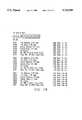
- FIG. 15shows an example decoding scheme for power control signal 236.
- receiver 206 in central terminal 10continues to monitor the amount of transmitting power from transmitter 204 for any changes resulting from power fluctuations, and variations in the path delay between central terminal 10 and subscriber terminal 20, et al. If the transmitting power falls below or exceeds the desired threshold range, central terminal 10 will send an appropriate power control signal 236 to increase or decrease the transmitting power of transmitter 204 as needed. At this point, adjustments made to return the transmitting power to the desired threshold range may occur in a fine adjustment mode having 0.1 decibel increments.
- central terminal 10may command transmitter 204 to return to a previous transmitting power level through recovery of parameters stored in a memory in subscriber terminal 20 in order to facilitate reestablishment of the appropriate communication path.
- transmitter 204 in subscriber terminal 20should be synchronized to receiver 206 in central terminal 10.
- Central terminal 10controls the synchronization of transmitter 204 through code synchronization signal 234 in overhead channel 224 of frame information signal 218.
- Code synchronization signal 234incrementally adjusts a phase of the slave code sequence of transmitter 204 to match the phase of the master code sequence of receiver 206. Synchronization of transmitter 204 is performed in a substantially similar manner as synchronization of receiver 202.
- Code synchronization signal 234is transmitted by transmitter 200 in central terminal 10 in overhead channel 224 of frame information signal 218 over downlink signal 212.
- Receiver 202 of subscriber terminal 20receives downlink signal 212 and extracts code synchronization signal 234 therefrom.
- Code synchronization signal 234is provided to transmitter 204 for incrementally adjustment of the phase of the slave code sequence of transmitter 204.
- Central terminal 10continues to incrementally adjust the phase of the slave code sequence of transmitter 204 until receiver 206 recognizes a code and phase match between the slave code sequence of transmitter 204 and the master code sequence of central terminal 10.
- Receiver 206performs the same power measurement technique in determining a phase and code match for transmitter 204 synchronization as performed for receiver 202 synchronization. Adjustments to the phase of the slave code sequence of transmitter 204 initially occur in a coarse adjustment mode having one half of a chip rate increments until receiver 206 identifies the maximum power position of the combined power of the master code sequence and the slave code sequence of transmitter 204.
- FIG. 16shows an example decoding scheme for code synchronization signal 234.
- receiver 206After identification and verification of a phase and code match of the slave code sequence to the master code sequence, receiver 206 continues to monitor uplink signal 214 for changes in the phase of the slave code sequence of transmitter 204 resulting from variations in the path delay between central terminal 10 and subscriber terminal 20. If further adjustments are needed to the phase of the slave code sequence of transmitter 204, central terminal 10 will send appropriate code synchronization signals 234 to increase or decrease the phase of the slave code sequence of transmitter 204 as needed. At this point, adjustments made to the phase of the slave code sequence of transmitter 204 may occur in a fine adjustment mode having one sixteenth of a chip rate increments. Upon an interruption in the downlink or uplink communication paths, central terminal 10 may command transmitter 204 to return to a previous slave code sequence phase value through recovery of parameters stored in a memory in subscriber terminal 20 in order to facilitate reestablishment of the appropriate communication path.
- receiver 206After synchronization of transmitter 204 is achieved, receiver 206 performs frame alignment on uplink signal 214 in a similar manner as frame alignment is performed by receiver 202 during establishment of the downlink communication path. Once receiver 206 recognizes two successive frame alignment words and obtains frame alignment, the uplink communication path has been established. Upon establishing both the downlink and the uplink communication paths, information transfer between first user 208 or second user 210 of subscriber terminal 20 and users coupled to central terminal 10 may commence.
- Wireless telecommunication system 1is capable of adjusting the transmitting power level and the transmit rate to one of two settings for each of three different system operating modes.
- the system operating modesare acquisition, standby and traffic. Adjustments in the transmitting power and the transmit rate make it possible to reduce and minimize interference with other subscriber terminals. Improvements in link establishment time are also achieved.
- the transmitting power levelis decoded in power control signal 236 and the transmit rate is decoded in code synchronization signal 234.
- the transmitting power for both downlink signal 212 and uplink signal 214can be set to either a nominal 0 decibel high power level or a reduced -12 decibel low power level.
- the transmit rate for both downlink signal 212 and uplink signal 214can be set to a low rate of 10 kilobits per second or a high rate of 160 kilobits per second.
- When switched to the high rate of 160 kilobits per seconduser traffic and overhead information are spread such that one information symbol results in the transmission of 16 chips. Correlation is performed over 16 chips, yielding a processing gain of 12 decibels.
- When switched to the low rate of 10 kilobits per secondonly overhead information is spread such that one overhead symbol results in the transmission of 256 chips. Correlation is performed over 256 chips, yielding a processing gain of 24 decibels.
- FIG. 17show the transmitting power and transmit rate for each of the three system operating modes.
- wireless telecommunication system 1enters the acquisition mode.
- the transmitting power of the downlink and uplink transmittersare maximized as well as the correlator processing gain. This maximizes the signal to noise ratio at the correlator output, increasing the amplitude of the correlation peak 219 for easier identification and minimal risk of false acquisition. Since only overhead information is needed in the acquisition mode, the transmit rate is at the low rate level of 10 kilobits per second.
- wireless telecommunication system 1When the downlink and the uplink communication paths are acquired, wireless telecommunication system 1 enters the standby mode. In the standby mode, the transmitting power of the downlink and uplink transmitters are reduced by 12 decibels. This reduction in transmitting power minimizes the interference to other subscriber terminals while still maintaining synchronization. The transmit rate remains at the low rate level to allow exchange of control information between central terminal 10 and subscriber terminal 20 over overhead channel 224.
- wireless telecommunication system 1When either an incoming or outgoing call is detected, a message is sent from the originating terminal to the destination terminal indicating that the downlink and uplink communication paths are required for the transmission of user traffic information. At this point, wireless telecommunication system 1 enters into the traffic mode. During the traffic mode, the transmitting power of both the downlink and uplink communication paths is increased to the high power level and the transmit rate is increased to the high rate level of 160 kilobits per second to facilitate information transfer between originating and destination terminals. Upon detection of call termination, a message is sent from the terminating terminal to the other terminal indicating that the downlink and uplink communication paths are no longer required. At this point, wireless telecommunication system 1 reenters the standby mode. Code synchronization and frame alignment tracking is performed in both the standby mode and the traffic mode.
- FIG. 18is a detailed block diagram of receiver 202 and transmitter 204 in subscriber terminal 20.
- Receiver 202receives downlink signal 212 at an RF receive interface 250.
- RF receive interface 250separates the spread spectrum signal into I and Q signal components.
- RF receive interface 250band pass filters each of the I and Q signal components by removing portions above approximately half of receiver 202 bandwidth of 3.5 MegaHertz.
- RF receive interface 250low pass filters the I and Q signal components to reject image frequencies and prevent signal aliasing.
- the I and Q signal componentsare placed into digital format by an analog to digital converter 252.
- the sampling frequency of analog to digital converter 252is four times the chip period, or 10.24 MegaHertz, with an eight bit resolution.
- the digital I and Q signal componentsare stepped to a rate of 5.12 MegaHertz by a down converter 254.
- a code generator and despreader 256performs the synchronization acquisition and tracking functions previously described to synchronize the phase of the Rademacher-Walsh and pseudo-random noise code sequence of receiver 202 to that of downlink signal 212.
- a digital signal processor 258controls the phase of the slave code sequence through a code tracker 260 and a carrier tracker 262.
- An automatic gain control unit 264produces an automatic gain control signal to control the gain of RF receive interface 250.
- Code generator and despreader 256generates the I and Q 160 kilobits per second of frame information for further synchronization by a node sync interface 266 under the control of a node sync logic unit 268.
- Node sync interface 266, through node sync logic unit 268,determines whether the I and Q channels should be swapped, as they may be received in four different ways.
- Viterbi decoder 270provides forward error correction on the I and Q channels and generates an error corrected 160 kilobits per second data signal after a 71 symbol delay.
- the error corrected signalis processed by a frame aligner and extractor 272 determines frame alignment and extracts power control signal 236, code synchronization 234, and operations and maintenance channel signal 238.
- Frame aligner and extractor 272also extracts first user channel 226 and second user channel 228 for traffic transmission towards first user 208 an second user 210, and signaling channel 230 for processing by high level data link controller 274 and a microcontroller 276.
- Frame aligner and extractor 272also provides alarm and error indications upon detecting a loss in frame alignment.
- a non-volatile random access memory 278stores system parameter information for subsequent insertion through an arbitrator 280 in the event of link loss in order to facilitate link reestablishment.
- Arbitrator 280also provides an interface between digital signal processor 258 and microcontroller 276.
- a frame inserter 282receives first user traffic and second user traffic from first user 208 and second user 210, signaling channel 230 information from high level data link controller 274, and operations and maintenance channel 238 information from microcontroller 276.
- Frame insertergenerates frame information signal 218 for uplink signal 214 for processing by a convolutional encoder 284.
- Convolutional encoder 284doubles the data rate of frame information signal 218 to provide forward error correction.
- a spreader 286splits the 320 kilobits per second signal of convolutional encoder 284 into two 160 kilobits per second I and Q signals and exclusively ORs these signals with the spreading sequence generated by a code generator 288 in response to a system clock generated by clock generator 290 as adjusted by code synchronization signal 234.
- Code generator 288generates one of sixteen Rademacher-Walsh functions exclusive ORed with a pseudo-random sequence having a pattern length of 256 with a chip rate of 2.56 MegaHertz.
- the pseudo-random sequenceshould match that of central terminal 10, but is adjustable under software control to provide reliable rejection of signals from other bands or other cells.
- Spreader 286supplies the I and Q signals to an analog transmitter 290.
- Analog transmitter 290produces pulsed I and Q signals for an RF transmit interface 292.
- Transmit poweris generated by first establishing a control voltage from a digital to analog converter in response to power control signal 236 extracted from overhead channel 224. This control voltage is applied to the power control inputs of analog transmitter 290 and RF transmit interface 292. Power control of 35 decibels is obtainable in both analog transmitter 290 and RF transmit interface 292.
- RF transmit interface 292includes a step attenuator that provides 2 decibel steps of attenuation over a 30 decibel range. This attenuator is used to switch between high and low power levels. On power up, maximum attenuation is selected to minimize the transmitting power of transmitter 204.
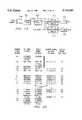
- FIG. 19is a block diagram of a CDMA signal processing circuit 100 within spreader 286.
- CDMA signal processing circuit 300includes a summer circuit 302 that receives a plurality of CDMA signals from a plurality of channels 304.
- Summer circuit 302generates a summed signal 306 that is applied to a clipping circuit 308.
- Clipping circuit 308generates a clipped signal 310 that is applied to an I digital to analog processing circuit 312 and a Q digital to analog processing circuit 314.
- Digital to analog processing circuit 312generates an I signal that is filtered by an I filter 316.
- Digital to analog processing circuit 314generates a Q signal that is filtered by a Q filter 318.
- CDMA signal processing circuit 300receives CDMA signals from the plurality of channels 304 at summer circuit 302.
- Each CDMA signalhas a disable value, a power magnitude value, and power direction value.
- the disable valuedetermines whether a CDMA signal is present on the particular channel.
- the power magnitude valueidentifies the relative power of the CDMA signal.
- the power magnitude valuepreferably has a low power value of 1 and a high power value of 4. Thus, the power magnitude value may be set at a first level representing an on-hook condition or a second level representing an off-hook condition.
- the power direction valuedetermines the positive or negative direction of the relative CDMA signal power and which of the I or Q signals the CDMA signal corresponds.
- Summer circuit 302combines the power values of each CDMA signal from the plurality of channels 304 to generate summed signal 306. For a sixteen channel circuit, summed signal 306 may range from -64 to +64 according to the power magnitude and direction values.
- Clipping circuit 308generates a clipped signal 310 in response to summed signal 306. Clipping circuit 308 removes a portion of summed signal 306 to improve handling of more frequently occurring values within a desired threshold range.
- FIG. 20shows selected values of summed signal 306 and selected values of clipped signal 310 generated in response thereto. Clipping circuit 308 removes that portion of summed signal 306 above and below a magnitude of ⁇ 31.
- a summed signal 306 occurring above the threshold magnitude of +31is set at the +31 magnitude level.
- a summed signal occurring below the threshold magnitude of -31is set at the -31 magnitude level.
- Removal of the portion of summed signal 306 outside the desired threshold rangealso eliminates noise producing sidebands from appearing on clipped signal 310 and increases the signal magnitude according to the desired threshold range. Elimination of noise producing sidebands results in more accurate and reliable I and Q signals. Though shown with a desired threshold range of approximately one half of summed signal 306, clipping circuit 308 may use a different threshold range selected to provide elimination of noise producing sidebands and improved handling of frequently occurring values of summed signal 306.
- Digital to analog processing circuits 312 and 314each receive clipped signal 310 generated by clipping circuit 308.
- Digital to analog processing circuits 312 and 314converts clipped signal 310 into a half width encoded format.
- FIG. 21shows an example of the half width encoded format.
- clipped signal 310is converted into a half width return to zero format wherein the first half of the chip period contains the information and the second half of the chip period contains no information.
- the half width encoded formatincreased power is obtained in the permitted band of frequencies for transmitted signals. More energy and information is within the passband of clipped signal 310 and the half width encoded format aids in information decoding at a far end receiver.
- digital to analog processing circuits 312 and 314convert clipped signal 310 into analog I and Q components, respectively.
- the outputs of digital to analog processing circuits 312 and 314are processed by I filter 316 and Q filter 318, respectively.
- Filters 316 and 318are used to significantly reduce inter-symbol interference between each half width encoded piece of the I and Q analog signals.
- FIG. 22shows an example of inter-symbol interference. Identifying transitions between half width encoded portions of an analog signal is important in reading and identifying information encoded in the analog signal. Preventing interference in the transition from one symbol of information to another aids in accurately and reliably reading information from analog signals.
- Filters 316 and 318provide a smoother rolloff and transition in the analog I and Q signals from one symbol to the next.
- a ninth order Besel filter operationmay be performed to minimize rolloff from a first symbol from affecting the next symbol.
- the ninth order Besel filterprovides a sufficient linear characteristic to achieve a desired reduction in inter-symbol interference.
- a CDMA signal processing circuitcombines CDMA signals from multiple channels to generate a summed signal in accordance with a power magnitude value and a power direction value associated with each CDMA signal. A portion of the summed signal outside a desired threshold range is removed to generate a clipped signal having noise producing sidebands from the outer area of the summed signal eliminated and to improve handling of frequently occurring values of the summed signal.
- the clipped signalis converted into a half width encoded format by a digital to analog processing circuit to increase desired frequency band power.
- the digital to analog processing circuittransforms the half width encoded clipped signal into a corresponding I and Q analog signal.
- the I and Q signalsare filtered to reduce inter-symbol interference between symbols of information half width encoded into the I and Q analog signals.
Landscapes
- Engineering & Computer Science (AREA)
- Computer Networks & Wireless Communication (AREA)
- Signal Processing (AREA)
- Software Systems (AREA)
- Theoretical Computer Science (AREA)
- Computer Security & Cryptography (AREA)
- Physics & Mathematics (AREA)
- General Engineering & Computer Science (AREA)
- General Physics & Mathematics (AREA)
- Human Computer Interaction (AREA)
- Mobile Radio Communication Systems (AREA)
- Tone Control, Compression And Expansion, Limiting Amplitude (AREA)
- Amplifiers (AREA)
- Reduction Or Emphasis Of Bandwidth Of Signals (AREA)
- Transmitters (AREA)
Abstract
Description
Claims (7)
Priority Applications (1)
| Application Number | Priority Date | Filing Date | Title |
|---|---|---|---|
| US09/063,232US6366570B1 (en) | 1995-06-02 | 1998-04-20 | Processing CDMA signals |
Applications Claiming Priority (6)
| Application Number | Priority Date | Filing Date | Title |
|---|---|---|---|
| GB9510870 | 1995-06-02 | ||
| GB9510870AGB2301751B (en) | 1995-06-02 | 1995-06-02 | Control message transmission in telecommunications systems |
| GB9511546AGB2301736B (en) | 1995-06-02 | 1995-06-07 | Apparatus and method of controlling transmitting power in a subscriber terminal of a wireless telecommunications systems |
| GB9511546 | 1995-06-07 | ||
| GB9513388 | 1995-06-30 | ||
| GB9513388AGB2301753A (en) | 1995-06-02 | 1995-06-30 | Processing CDMA signals |
Related Child Applications (1)
| Application Number | Title | Priority Date | Filing Date |
|---|---|---|---|
| US09/063,232ContinuationUS6366570B1 (en) | 1995-06-02 | 1998-04-20 | Processing CDMA signals |
Publications (1)
| Publication Number | Publication Date |
|---|---|
| US5742595Atrue US5742595A (en) | 1998-04-21 |
Family
ID=27267749
Family Applications (2)
| Application Number | Title | Priority Date | Filing Date |
|---|---|---|---|
| US08/558,675Expired - LifetimeUS5742595A (en) | 1995-06-02 | 1995-11-16 | Processing CDMA signals |
| US09/063,232Expired - LifetimeUS6366570B1 (en) | 1995-06-02 | 1998-04-20 | Processing CDMA signals |
Family Applications After (1)
| Application Number | Title | Priority Date | Filing Date |
|---|---|---|---|
| US09/063,232Expired - LifetimeUS6366570B1 (en) | 1995-06-02 | 1998-04-20 | Processing CDMA signals |
Country Status (9)
| Country | Link |
|---|---|
| US (2) | US5742595A (en) |
| EP (1) | EP0829150B1 (en) |
| JP (1) | JPH11506584A (en) |
| CN (1) | CN1194071A (en) |
| AU (1) | AU710839B2 (en) |
| BR (1) | BR9609468A (en) |
| CA (1) | CA2222734C (en) |
| DE (1) | DE69629465T2 (en) |
| WO (1) | WO1996038944A1 (en) |
Cited By (14)
| Publication number | Priority date | Publication date | Assignee | Title |
|---|---|---|---|---|
| EP0940925A1 (en)* | 1998-03-05 | 1999-09-08 | Lucent Technologies Inc. | System and method to reduce the peak-to-average power ratio in a DS-CMDA transmitter |
| US6018546A (en)* | 1997-09-16 | 2000-01-25 | Lucent Technologies Inc. | Technique for soft decision metric generation in a wireless communications system |
| WO2000013337A3 (en)* | 1998-08-31 | 2000-06-08 | Qualcomm Inc | Method and apparatus for reducing amplitude variations in communication signals employing inserted pilot symbol |
| US6144694A (en)* | 1996-10-17 | 2000-11-07 | Hitachi, Ltd. | Transmitting apparatus for code division multiplexed signals |
| EP1058400A3 (en)* | 1999-06-02 | 2002-03-27 | Nortel Networks Limited | Method & apparatus for reducing the peak power probability of a spread spectrum signal |
| WO2001052440A3 (en)* | 2000-01-14 | 2002-06-06 | Siemens Ag | Power control in mobile radio telephone systems when transmission is interrupted |
| US20020071420A1 (en)* | 1997-10-31 | 2002-06-13 | Interdigital Technology Corporation | CDMA base station having an improved antenna system |
| WO2002075949A1 (en)* | 2001-02-17 | 2002-09-26 | Casuh Corporation | Multiple phase cdma modulation and demodulation method and apparatus |
| WO2003032511A1 (en)* | 2001-10-08 | 2003-04-17 | Casuh Co., Ltd. | Code-select cdma modulation/demodulation method and device thereof |
| US20030224822A1 (en)* | 2002-05-16 | 2003-12-04 | Korea Electronics Technology Institute | Apparatus for transmitting data in a wireless communication system |
| US6687238B1 (en)* | 1999-03-10 | 2004-02-03 | Qualcomm Incorporated | CDMA signal transmission control |
| SG109974A1 (en)* | 1999-08-31 | 2005-04-28 | Interdigital Tech Corp | Adaptive rf amplifier prelimiter |
| US6956840B1 (en)* | 1998-09-21 | 2005-10-18 | Ipr Licensing, Inc. | Power control protocol for highly variable data rate reverse link of a wireless communication system |
| US7715461B2 (en) | 1996-05-28 | 2010-05-11 | Qualcomm, Incorporated | High data rate CDMA wireless communication system using variable sized channel codes |
Families Citing this family (54)
| Publication number | Priority date | Publication date | Assignee | Title |
|---|---|---|---|---|
| US6226259B1 (en) | 1997-04-29 | 2001-05-01 | Canon Kabushiki Kaisha | Device and method for transmitting information device and method for processing information |
| US6542481B2 (en) | 1998-06-01 | 2003-04-01 | Tantivy Communications, Inc. | Dynamic bandwidth allocation for multiple access communication using session queues |
| US6151332A (en) | 1997-06-20 | 2000-11-21 | Tantivy Communications, Inc. | Protocol conversion and bandwidth reduction technique providing multiple nB+D ISDN basic rate interface links over a wireless code division multiple access communication system |
| US6081536A (en)* | 1997-06-20 | 2000-06-27 | Tantivy Communications, Inc. | Dynamic bandwidth allocation to transmit a wireless protocol across a code division multiple access (CDMA) radio link |
| US6222832B1 (en)* | 1998-06-01 | 2001-04-24 | Tantivy Communications, Inc. | Fast Acquisition of traffic channels for a highly variable data rate reverse link of a CDMA wireless communication system |
| US7936728B2 (en) | 1997-12-17 | 2011-05-03 | Tantivy Communications, Inc. | System and method for maintaining timing of synchronization messages over a reverse link of a CDMA wireless communication system |
| US7394791B2 (en) | 1997-12-17 | 2008-07-01 | Interdigital Technology Corporation | Multi-detection of heartbeat to reduce error probability |
| US7496072B2 (en)* | 1997-12-17 | 2009-02-24 | Interdigital Technology Corporation | System and method for controlling signal strength over a reverse link of a CDMA wireless communication system |
| US9525923B2 (en) | 1997-12-17 | 2016-12-20 | Intel Corporation | Multi-detection of heartbeat to reduce error probability |
| US20040160910A1 (en)* | 1997-12-17 | 2004-08-19 | Tantivy Communications, Inc. | Dynamic bandwidth allocation to transmit a wireless protocol across a code division multiple access (CDMA) radio link |
| US8175120B2 (en) | 2000-02-07 | 2012-05-08 | Ipr Licensing, Inc. | Minimal maintenance link to support synchronization |
| US6266320B1 (en)* | 1998-04-08 | 2001-07-24 | Telefonaktiebolaget Lm Ericsson (Publ) | Amplitude limitation in CDMA system |
| US8134980B2 (en) | 1998-06-01 | 2012-03-13 | Ipr Licensing, Inc. | Transmittal of heartbeat signal at a lower level than heartbeat request |
| US7773566B2 (en) | 1998-06-01 | 2010-08-10 | Tantivy Communications, Inc. | System and method for maintaining timing of synchronization messages over a reverse link of a CDMA wireless communication system |
| US7221664B2 (en)* | 1998-06-01 | 2007-05-22 | Interdigital Technology Corporation | Transmittal of heartbeat signal at a lower level than heartbeat request |
| US7376105B2 (en)* | 1998-08-21 | 2008-05-20 | Massachusetts Institute Of Technology | Source coding for interference reduction |
| EP1286480B1 (en)* | 1998-10-09 | 2007-02-14 | Siemens Aktiengesellschaft | Method for regulating power between a base station and a subscriber station |
| US6620173B2 (en) | 1998-12-08 | 2003-09-16 | Intuitive Surgical, Inc. | Method for introducing an end effector to a surgical site in minimally invasive surgery |
| SE513863C2 (en) | 1999-01-29 | 2000-11-20 | Ericsson Telefon Ab L M | Method and apparatus for cutting in a CDMA system |
| US6614776B1 (en)* | 1999-04-28 | 2003-09-02 | Tantivy Communications, Inc. | Forward error correction scheme for high rate data exchange in a wireless system |
| US6526034B1 (en) | 1999-09-21 | 2003-02-25 | Tantivy Communications, Inc. | Dual mode subscriber unit for short range, high rate and long range, lower rate data communications |
| US8463255B2 (en)* | 1999-12-20 | 2013-06-11 | Ipr Licensing, Inc. | Method and apparatus for a spectrally compliant cellular communication system |
| US6912228B1 (en)* | 2000-04-14 | 2005-06-28 | Telefonaktiebolaget L M Ericsson (Publ) | Power control in a radio data communication system adapted using transmission load |
| WO2002041530A1 (en)* | 2000-11-16 | 2002-05-23 | Sony Corporation | Information processing apparatus and communication apparatus |
| US8155096B1 (en) | 2000-12-01 | 2012-04-10 | Ipr Licensing Inc. | Antenna control system and method |
| US8964604B2 (en) | 2000-12-26 | 2015-02-24 | Polycom, Inc. | Conference endpoint instructing conference bridge to dial phone number |
| US7339605B2 (en) | 2004-04-16 | 2008-03-04 | Polycom, Inc. | Conference link between a speakerphone and a video conference unit |
| US8977683B2 (en) | 2000-12-26 | 2015-03-10 | Polycom, Inc. | Speakerphone transmitting password information to a remote device |
| US8948059B2 (en) | 2000-12-26 | 2015-02-03 | Polycom, Inc. | Conference endpoint controlling audio volume of a remote device |
| US9001702B2 (en) | 2000-12-26 | 2015-04-07 | Polycom, Inc. | Speakerphone using a secure audio connection to initiate a second secure connection |
| US6954448B2 (en) | 2001-02-01 | 2005-10-11 | Ipr Licensing, Inc. | Alternate channel for carrying selected message types |
| US7551663B1 (en) | 2001-02-01 | 2009-06-23 | Ipr Licensing, Inc. | Use of correlation combination to achieve channel detection |
| GB0110125D0 (en) | 2001-04-25 | 2001-06-20 | Koninkl Philips Electronics Nv | Radio communication system |
| US8934382B2 (en) | 2001-05-10 | 2015-01-13 | Polycom, Inc. | Conference endpoint controlling functions of a remote device |
| US8976712B2 (en) | 2001-05-10 | 2015-03-10 | Polycom, Inc. | Speakerphone and conference bridge which request and perform polling operations |
| CA2867406C (en) | 2001-06-13 | 2016-08-02 | Intel Corporation | Transmittal of heartbeat signal at a lower level than heartbeat request |
| FI20012059A0 (en)* | 2001-10-24 | 2001-10-24 | Nokia Corp | Method and arrangement for limiting the signal in a radio transmitter |
| US8102984B2 (en) | 2001-12-31 | 2012-01-24 | Polycom Inc. | Speakerphone and conference bridge which receive and provide participant monitoring information |
| US8144854B2 (en) | 2001-12-31 | 2012-03-27 | Polycom Inc. | Conference bridge which detects control information embedded in audio information to prioritize operations |
| US8223942B2 (en)* | 2001-12-31 | 2012-07-17 | Polycom, Inc. | Conference endpoint requesting and receiving billing information from a conference bridge |
| US7978838B2 (en) | 2001-12-31 | 2011-07-12 | Polycom, Inc. | Conference endpoint instructing conference bridge to mute participants |
| US8885523B2 (en) | 2001-12-31 | 2014-11-11 | Polycom, Inc. | Speakerphone transmitting control information embedded in audio information through a conference bridge |
| US8947487B2 (en) | 2001-12-31 | 2015-02-03 | Polycom, Inc. | Method and apparatus for combining speakerphone and video conference unit operations |
| US8934381B2 (en)* | 2001-12-31 | 2015-01-13 | Polycom, Inc. | Conference endpoint instructing a remote device to establish a new connection |
| US8705719B2 (en) | 2001-12-31 | 2014-04-22 | Polycom, Inc. | Speakerphone and conference bridge which receive and provide participant monitoring information |
| US20030162573A1 (en)* | 2002-02-19 | 2003-08-28 | Jyhchau Horng | Down-link interference cancellation for high-data-rate channels in advanced digital wireless networks |
| US7054656B2 (en)* | 2002-08-02 | 2006-05-30 | Motorola, Inc. | Method and apparatus for provision of non-power control information through a power control channel to a mobile station |
| US6922160B1 (en)* | 2002-10-09 | 2005-07-26 | Unisys Corporation | Scalable bus system and method for communicating digital data using analog modulation and demodulation |
| KR101222447B1 (en)* | 2004-07-15 | 2013-01-15 | 큐빅 코포레이션 | Enhancement of aimpoint in simulated training systems |
| US8199791B2 (en)* | 2005-06-08 | 2012-06-12 | Polycom, Inc. | Mixed voice and spread spectrum data signaling with enhanced concealment of data |
| US8126029B2 (en) | 2005-06-08 | 2012-02-28 | Polycom, Inc. | Voice interference correction for mixed voice and spread spectrum data signaling |
| KR101083944B1 (en)* | 2005-12-21 | 2011-11-15 | 엘지에릭슨 주식회사 | Adaptive CFR according to average power variation of input signal and method thereof |
| US8064330B2 (en)* | 2008-03-26 | 2011-11-22 | Qualcomm Incorporated | Bit-width minimization scheme for wireless communication |
| US9179430B2 (en)* | 2012-01-18 | 2015-11-03 | Extenet Systems, Inc. | PN selection for RF repeaters, bi-directional amplifiers or distributed antenna systems |
Citations (60)
| Publication number | Priority date | Publication date | Assignee | Title |
|---|---|---|---|---|
| US4207526A (en)* | 1978-04-05 | 1980-06-10 | Rca Corporation | Pre-processing apparatus for FM stereo overshoot elimination |
| US4415900A (en)* | 1981-12-28 | 1983-11-15 | The United States Of America As Represented By The Secretary Of The Navy | Cavity/microstrip multi-mode antenna |
| EP0097028A2 (en)* | 1982-06-10 | 1983-12-28 | Fuji Xerox Co., Ltd. | Multiple-microcomputer communications system |
| US4449061A (en)* | 1980-06-17 | 1984-05-15 | Sony Corporation | Wave-shaping circuit for digital signal |
| GB2132454A (en)* | 1982-12-27 | 1984-07-04 | Western Electric Co | Improvements in or relating to radio communication apparatus and systems |
| US4538281A (en)* | 1982-05-06 | 1985-08-27 | Rockwell International Corporation | Adaptive acquisition of multiple access codes |
| GB2172775A (en)* | 1985-03-19 | 1986-09-24 | Oki Electric Ind Co Ltd | Cellular radio telephone system |
| EP0240821A2 (en)* | 1986-04-09 | 1987-10-14 | Siemens Aktiengesellschaft | Method for the transmission of digital signals in a mobile radio system |
| WO1987007408A1 (en)* | 1986-05-20 | 1987-12-03 | American Telephone & Telegraph Company | Information transfer method and arrangement |
| US4737975A (en)* | 1984-09-18 | 1988-04-12 | Metrofone, Inc. | Programmable system for interfacing a standard telephone set with a radio transceiver |
| US4763324A (en)* | 1986-02-10 | 1988-08-09 | Siemens Aktiengesellschaft | Frame decoding |
| US4777653A (en)* | 1985-12-20 | 1988-10-11 | Telecommunications Radioelectriques Et Telephoniques T.R.T. | Apparatus for controlling transmission power over a digital radio communication channel |
| US4779265A (en)* | 1986-10-27 | 1988-10-18 | Bell Communications Research, Inc. | Multiple access communication system |
| US4779266A (en)* | 1986-03-10 | 1988-10-18 | Bell Communications Research, Inc. | Encoding and decoding for code division multiple access communication systems |
| US4801934A (en)* | 1984-10-04 | 1989-01-31 | Siemens Aktiengesellschaft | Method and apparatus for transmission of data with data reduction |
| WO1989007377A1 (en)* | 1988-01-29 | 1989-08-10 | Network Equipment Technologies, Inc. | Communications network state and topology monitor |
| US4864565A (en)* | 1986-09-29 | 1989-09-05 | Siemens Aktiengesellschaft | Method for frame synchronization of an exchange of a PCM time multiplex telecommunication system |
| GB2222504A (en)* | 1987-06-24 | 1990-03-07 | Westinghouse Electric Corp | Multiprocessor information exchange |
| EP0364189A2 (en)* | 1988-10-10 | 1990-04-18 | Vickers Shipbuilding & Engineering Limited | System design tool and method |
| GB2229320A (en)* | 1989-01-20 | 1990-09-19 | Antenna Products Ltd | Antenna |
| US4965759A (en)* | 1988-01-14 | 1990-10-23 | Clarion Co., Ltd. | Spread-spectrum receiver |
| WO1990013962A1 (en)* | 1989-05-10 | 1990-11-15 | Motorola, Inc. | Dialing features for cellular telephone with standard telephone set |
| US5020055A (en)* | 1989-06-23 | 1991-05-28 | May Jr Carl J | Multi-length packet format including fixed length information words |
| GB2241851A (en)* | 1990-03-09 | 1991-09-11 | Philips Electronic Associated | Optimising transmitter power in a communications system |
| US5054070A (en)* | 1990-03-05 | 1991-10-01 | Qei Corporation | Stereo signal communication system and method |
| GB2243267A (en)* | 1990-04-21 | 1991-10-23 | Stc Plc | Telecommunication |
| GB2248007A (en)* | 1990-06-29 | 1992-03-18 | Digital Equipment Corp | Local area network terminal server with data movement module |
| US5099493A (en)* | 1990-08-27 | 1992-03-24 | Zeger-Abrams Incorporated | Multiple signal receiver for direct sequence, code division multiple access, spread spectrum signals |
| US5101417A (en)* | 1990-06-29 | 1992-03-31 | Xerox Corporation | Phase controlled synchronization for direct sequence spread-spectrum communication systems |
| US5103459A (en)* | 1990-06-25 | 1992-04-07 | Qualcomm Incorporated | System and method for generating signal waveforms in a cdma cellular telephone system |
| US5136612A (en)* | 1990-12-31 | 1992-08-04 | At&T Bell Laboratories | Method and apparatus for reducing effects of multiple access interference in a radio receiver in a code division multiple access communication system |
| US5189674A (en)* | 1989-07-11 | 1993-02-23 | Nec Corporation | Fault locating system capable of quickly locating a fault in a hierarchical communication network |
| EP0529207A1 (en)* | 1991-06-05 | 1993-03-03 | Robert Bosch Gmbh | Method for controlling and supervising a telecommunication-network |
| WO1993007702A1 (en)* | 1991-10-08 | 1993-04-15 | Qualcomm Incorporated | Transmitter power control system |
| US5220335A (en)* | 1990-03-30 | 1993-06-15 | The United States Of America As Represented By The Administrator Of The National Aeronautics And Space Administration | Planar microstrip Yagi antenna array |
| US5237586A (en)* | 1992-03-25 | 1993-08-17 | Ericsson-Ge Mobile Communications Holding, Inc. | Rake receiver with selective ray combining |
| GB2264375A (en)* | 1992-02-12 | 1993-08-25 | Samsung Electronics Co Ltd | Auto-switching device for cpu logic circuits. |
| EP0565507A2 (en)* | 1992-04-10 | 1993-10-13 | Ericsson Inc. | Power control for random access call set-up in a mobile telephone system |
| GB2268293A (en)* | 1992-06-17 | 1994-01-05 | Texas Instruments Ltd | Installing a resident part of a Terminate and Stay Resident program. |
| EP0582537A2 (en)* | 1992-08-07 | 1994-02-09 | International Business Machines Corporation | Transmission of high-priority, real-time traffic on low-speed communications links |
| US5289470A (en)* | 1992-12-14 | 1994-02-22 | International Business Machines Corp. | Flexible scheme for buffer space allocation in networking devices |
| US5307405A (en)* | 1992-09-25 | 1994-04-26 | Qualcomm Incorporated | Network echo canceller |
| GB2272610A (en)* | 1992-11-12 | 1994-05-18 | Northern Telecom Ltd | Method of introducing additional outstations into TDMA telecommunication systems |
| WO1994021057A1 (en)* | 1993-03-01 | 1994-09-15 | Telefonaktiebolaget Lm Ericsson | A method and an apparatus for handing off mobile station from a first to a second channel in a mobile communication system |
| US5353300A (en)* | 1993-06-07 | 1994-10-04 | Motorola, Inc. | Communication method for an adaptive direct sequence CDMA communication system |
| US5359624A (en)* | 1993-06-07 | 1994-10-25 | Motorola, Inc. | System and method for chip timing synchronization in an adaptive direct sequence CDMA communication system |
| GB2277425A (en)* | 1993-04-23 | 1994-10-26 | Motorola Inc | A message communication system for transferring messages between a host processor and peripherals |
| GB2278260A (en)* | 1990-12-21 | 1994-11-23 | Motorola Inc | Method and apparatus for cancelling spread-spectrum noise |
| US5381446A (en)* | 1993-06-25 | 1995-01-10 | Digital Wireless Corp. | Digital implementation of spread spectrum communications system |
| WO1995002950A1 (en)* | 1993-07-14 | 1995-01-26 | Nokia Telecommunications Oy | A method for adjusting transmission power in a cellular radio system and a subscriber equipment |
| GB2282510A (en)* | 1993-09-07 | 1995-04-05 | Motorola Ltd | A data network |
| US5418818A (en)* | 1992-09-22 | 1995-05-23 | Glenayre Electronics, Inc. | Digital signal processor exciter |
| US5418814A (en)* | 1993-07-01 | 1995-05-23 | Roke Manor Research Limited | Threshold cancellation means for use in digital mobile radio networks |
| US5418815A (en)* | 1992-06-12 | 1995-05-23 | Kabushiki Kaisha Toshiba | Receiver adaptively operable for multiple signal transmission systems |
| WO1995017785A1 (en)* | 1993-12-20 | 1995-06-29 | Csir | Direct conversion cdma receiver |
| GB2286317A (en)* | 1994-02-07 | 1995-08-09 | Fujitsu Ltd | Centralized network monitoring device |
| US5450425A (en)* | 1993-11-19 | 1995-09-12 | Multi-Tech Systems, Inc. | Protocol for communication of a data packet |
| GB2287379A (en)* | 1994-03-10 | 1995-09-13 | Roke Manor Research | Mobile power control and selection of base station in a CDMA cellular system |
| EP0680157A1 (en)* | 1994-04-29 | 1995-11-02 | AT&T Corp. | Methods of and devices for spread spectrum communication systems using forward error correction |
| EP0681376A2 (en)* | 1994-04-29 | 1995-11-08 | AT&T Corp. | Methods of and devices for spread spectrum communication systems using forward error correction |
Family Cites Families (3)
| Publication number | Priority date | Publication date | Assignee | Title |
|---|---|---|---|---|
| US4013842A (en)* | 1976-04-15 | 1977-03-22 | Bell Telephone Laboratories, Incorporated | Method and apparatus for interfacing digital and analog carrier systems |
| JPH04347943A (en)* | 1990-11-13 | 1992-12-03 | Ricoh Co Ltd | Spectrum spread communication system, synchronizing system, and modulating/demodulating system |
| JP3143256B2 (en) | 1993-03-16 | 2001-03-07 | 稔 稲津 | Code division multiplex system |
- 1995
- 1995-11-16USUS08/558,675patent/US5742595A/ennot_activeExpired - Lifetime
- 1996
- 1996-06-03CACA002222734Apatent/CA2222734C/ennot_activeExpired - Fee Related
- 1996-06-03DEDE69629465Tpatent/DE69629465T2/ennot_activeExpired - Lifetime
- 1996-06-03CNCN96195270Apatent/CN1194071A/enactivePending
- 1996-06-03AUAU59728/96Apatent/AU710839B2/ennot_activeCeased
- 1996-06-03EPEP96917034Apatent/EP0829150B1/ennot_activeExpired - Lifetime
- 1996-06-03WOPCT/US1996/008500patent/WO1996038944A1/enactiveIP Right Grant
- 1996-06-03BRBR9609468Apatent/BR9609468A/ennot_activeApplication Discontinuation
- 1996-06-03JPJP8536784Apatent/JPH11506584A/ennot_activeCeased
- 1998
- 1998-04-20USUS09/063,232patent/US6366570B1/ennot_activeExpired - Lifetime
Patent Citations (61)
| Publication number | Priority date | Publication date | Assignee | Title |
|---|---|---|---|---|
| US4207526A (en)* | 1978-04-05 | 1980-06-10 | Rca Corporation | Pre-processing apparatus for FM stereo overshoot elimination |
| US4449061A (en)* | 1980-06-17 | 1984-05-15 | Sony Corporation | Wave-shaping circuit for digital signal |
| US4415900A (en)* | 1981-12-28 | 1983-11-15 | The United States Of America As Represented By The Secretary Of The Navy | Cavity/microstrip multi-mode antenna |
| US4538281A (en)* | 1982-05-06 | 1985-08-27 | Rockwell International Corporation | Adaptive acquisition of multiple access codes |
| EP0097028A2 (en)* | 1982-06-10 | 1983-12-28 | Fuji Xerox Co., Ltd. | Multiple-microcomputer communications system |
| GB2132454A (en)* | 1982-12-27 | 1984-07-04 | Western Electric Co | Improvements in or relating to radio communication apparatus and systems |
| US4737975A (en)* | 1984-09-18 | 1988-04-12 | Metrofone, Inc. | Programmable system for interfacing a standard telephone set with a radio transceiver |
| US4801934A (en)* | 1984-10-04 | 1989-01-31 | Siemens Aktiengesellschaft | Method and apparatus for transmission of data with data reduction |
| GB2172775A (en)* | 1985-03-19 | 1986-09-24 | Oki Electric Ind Co Ltd | Cellular radio telephone system |
| US4777653A (en)* | 1985-12-20 | 1988-10-11 | Telecommunications Radioelectriques Et Telephoniques T.R.T. | Apparatus for controlling transmission power over a digital radio communication channel |
| US4763324A (en)* | 1986-02-10 | 1988-08-09 | Siemens Aktiengesellschaft | Frame decoding |
| US4779266A (en)* | 1986-03-10 | 1988-10-18 | Bell Communications Research, Inc. | Encoding and decoding for code division multiple access communication systems |
| EP0240821A2 (en)* | 1986-04-09 | 1987-10-14 | Siemens Aktiengesellschaft | Method for the transmission of digital signals in a mobile radio system |
| WO1987007408A1 (en)* | 1986-05-20 | 1987-12-03 | American Telephone & Telegraph Company | Information transfer method and arrangement |
| US4864565A (en)* | 1986-09-29 | 1989-09-05 | Siemens Aktiengesellschaft | Method for frame synchronization of an exchange of a PCM time multiplex telecommunication system |
| US4779265A (en)* | 1986-10-27 | 1988-10-18 | Bell Communications Research, Inc. | Multiple access communication system |
| GB2222504A (en)* | 1987-06-24 | 1990-03-07 | Westinghouse Electric Corp | Multiprocessor information exchange |
| US4965759A (en)* | 1988-01-14 | 1990-10-23 | Clarion Co., Ltd. | Spread-spectrum receiver |
| WO1989007377A1 (en)* | 1988-01-29 | 1989-08-10 | Network Equipment Technologies, Inc. | Communications network state and topology monitor |
| EP0364189A2 (en)* | 1988-10-10 | 1990-04-18 | Vickers Shipbuilding & Engineering Limited | System design tool and method |
| GB2229320A (en)* | 1989-01-20 | 1990-09-19 | Antenna Products Ltd | Antenna |
| WO1990013962A1 (en)* | 1989-05-10 | 1990-11-15 | Motorola, Inc. | Dialing features for cellular telephone with standard telephone set |
| US5020055A (en)* | 1989-06-23 | 1991-05-28 | May Jr Carl J | Multi-length packet format including fixed length information words |
| US5189674A (en)* | 1989-07-11 | 1993-02-23 | Nec Corporation | Fault locating system capable of quickly locating a fault in a hierarchical communication network |
| US5054070A (en)* | 1990-03-05 | 1991-10-01 | Qei Corporation | Stereo signal communication system and method |
| GB2241851A (en)* | 1990-03-09 | 1991-09-11 | Philips Electronic Associated | Optimising transmitter power in a communications system |
| US5220335A (en)* | 1990-03-30 | 1993-06-15 | The United States Of America As Represented By The Administrator Of The National Aeronautics And Space Administration | Planar microstrip Yagi antenna array |
| GB2243267A (en)* | 1990-04-21 | 1991-10-23 | Stc Plc | Telecommunication |
| US5103459A (en)* | 1990-06-25 | 1992-04-07 | Qualcomm Incorporated | System and method for generating signal waveforms in a cdma cellular telephone system |
| US5103459B1 (en)* | 1990-06-25 | 1999-07-06 | Qualcomm Inc | System and method for generating signal waveforms in a cdma cellular telephone system |
| GB2248007A (en)* | 1990-06-29 | 1992-03-18 | Digital Equipment Corp | Local area network terminal server with data movement module |
| US5101417A (en)* | 1990-06-29 | 1992-03-31 | Xerox Corporation | Phase controlled synchronization for direct sequence spread-spectrum communication systems |
| US5099493A (en)* | 1990-08-27 | 1992-03-24 | Zeger-Abrams Incorporated | Multiple signal receiver for direct sequence, code division multiple access, spread spectrum signals |
| GB2278260A (en)* | 1990-12-21 | 1994-11-23 | Motorola Inc | Method and apparatus for cancelling spread-spectrum noise |
| US5136612A (en)* | 1990-12-31 | 1992-08-04 | At&T Bell Laboratories | Method and apparatus for reducing effects of multiple access interference in a radio receiver in a code division multiple access communication system |
| EP0529207A1 (en)* | 1991-06-05 | 1993-03-03 | Robert Bosch Gmbh | Method for controlling and supervising a telecommunication-network |
| WO1993007702A1 (en)* | 1991-10-08 | 1993-04-15 | Qualcomm Incorporated | Transmitter power control system |
| GB2264375A (en)* | 1992-02-12 | 1993-08-25 | Samsung Electronics Co Ltd | Auto-switching device for cpu logic circuits. |
| US5237586A (en)* | 1992-03-25 | 1993-08-17 | Ericsson-Ge Mobile Communications Holding, Inc. | Rake receiver with selective ray combining |
| EP0565507A2 (en)* | 1992-04-10 | 1993-10-13 | Ericsson Inc. | Power control for random access call set-up in a mobile telephone system |
| US5418815A (en)* | 1992-06-12 | 1995-05-23 | Kabushiki Kaisha Toshiba | Receiver adaptively operable for multiple signal transmission systems |
| GB2268293A (en)* | 1992-06-17 | 1994-01-05 | Texas Instruments Ltd | Installing a resident part of a Terminate and Stay Resident program. |
| EP0582537A2 (en)* | 1992-08-07 | 1994-02-09 | International Business Machines Corporation | Transmission of high-priority, real-time traffic on low-speed communications links |
| US5418818A (en)* | 1992-09-22 | 1995-05-23 | Glenayre Electronics, Inc. | Digital signal processor exciter |
| US5307405A (en)* | 1992-09-25 | 1994-04-26 | Qualcomm Incorporated | Network echo canceller |
| GB2272610A (en)* | 1992-11-12 | 1994-05-18 | Northern Telecom Ltd | Method of introducing additional outstations into TDMA telecommunication systems |
| US5289470A (en)* | 1992-12-14 | 1994-02-22 | International Business Machines Corp. | Flexible scheme for buffer space allocation in networking devices |
| WO1994021057A1 (en)* | 1993-03-01 | 1994-09-15 | Telefonaktiebolaget Lm Ericsson | A method and an apparatus for handing off mobile station from a first to a second channel in a mobile communication system |
| GB2277425A (en)* | 1993-04-23 | 1994-10-26 | Motorola Inc | A message communication system for transferring messages between a host processor and peripherals |
| US5359624A (en)* | 1993-06-07 | 1994-10-25 | Motorola, Inc. | System and method for chip timing synchronization in an adaptive direct sequence CDMA communication system |
| US5353300A (en)* | 1993-06-07 | 1994-10-04 | Motorola, Inc. | Communication method for an adaptive direct sequence CDMA communication system |
| US5381446A (en)* | 1993-06-25 | 1995-01-10 | Digital Wireless Corp. | Digital implementation of spread spectrum communications system |
| US5418814A (en)* | 1993-07-01 | 1995-05-23 | Roke Manor Research Limited | Threshold cancellation means for use in digital mobile radio networks |
| WO1995002950A1 (en)* | 1993-07-14 | 1995-01-26 | Nokia Telecommunications Oy | A method for adjusting transmission power in a cellular radio system and a subscriber equipment |
| GB2282510A (en)* | 1993-09-07 | 1995-04-05 | Motorola Ltd | A data network |
| US5450425A (en)* | 1993-11-19 | 1995-09-12 | Multi-Tech Systems, Inc. | Protocol for communication of a data packet |
| WO1995017785A1 (en)* | 1993-12-20 | 1995-06-29 | Csir | Direct conversion cdma receiver |
| GB2286317A (en)* | 1994-02-07 | 1995-08-09 | Fujitsu Ltd | Centralized network monitoring device |
| GB2287379A (en)* | 1994-03-10 | 1995-09-13 | Roke Manor Research | Mobile power control and selection of base station in a CDMA cellular system |
| EP0680157A1 (en)* | 1994-04-29 | 1995-11-02 | AT&T Corp. | Methods of and devices for spread spectrum communication systems using forward error correction |
| EP0681376A2 (en)* | 1994-04-29 | 1995-11-08 | AT&T Corp. | Methods of and devices for spread spectrum communication systems using forward error correction |
Non-Patent Citations (5)
| Title |
|---|
| Faith M. Ozluturk and Gary Lomp, "Effect of Limiting the Downlink Power in CDMA Systems with or without Forward Power Control", 1995 IEEE, pp. 952-956. |
| Faith M. Ozluturk and Gary Lomp, Effect of Limiting the Downlink Power in CDMA Systems with or without Forward Power Control , 1995 IEEE , pp. 952 956.* |
| PCT International Search Report, dated Sep. 25, 1996.* |
| Sedra et al., Microelectronic Circuit, Sauders College Publishing, pp. 163 164, 1991.* |
| Sedra et al., Microelectronic Circuit, Sauders College Publishing, pp. 163-164, 1991. |
Cited By (37)
| Publication number | Priority date | Publication date | Assignee | Title |
|---|---|---|---|---|
| US8588277B2 (en) | 1996-05-28 | 2013-11-19 | Qualcomm Incorporated | High data rate CDMA wireless communication system using variable sized channel codes |
| US8213485B2 (en) | 1996-05-28 | 2012-07-03 | Qualcomm Incorporated | High rate CDMA wireless communication system using variable sized channel codes |
| US7715461B2 (en) | 1996-05-28 | 2010-05-11 | Qualcomm, Incorporated | High data rate CDMA wireless communication system using variable sized channel codes |
| US6144694A (en)* | 1996-10-17 | 2000-11-07 | Hitachi, Ltd. | Transmitting apparatus for code division multiplexed signals |
| US6018546A (en)* | 1997-09-16 | 2000-01-25 | Lucent Technologies Inc. | Technique for soft decision metric generation in a wireless communications system |
| US6584091B2 (en)* | 1997-10-31 | 2003-06-24 | Interdigital Technology Corporation | CDMA base station having an improved antenna system |
| US20030043776A1 (en)* | 1997-10-31 | 2003-03-06 | Interdigital Technology Corporation | CDMA base station having an improved antenna system |
| US20070091865A1 (en)* | 1997-10-31 | 2007-04-26 | Interdigital Technology Corporation | Communication station having an improved antenna system |
| US20020071420A1 (en)* | 1997-10-31 | 2002-06-13 | Interdigital Technology Corporation | CDMA base station having an improved antenna system |
| US20020093932A1 (en)* | 1997-10-31 | 2002-07-18 | Interdigital Technology Corporation | CDMA subscriber unit having an improved antenna system |
| US6452918B1 (en)* | 1997-10-31 | 2002-09-17 | Interdigital Technology Corporation | CDMA subscriber unit having an improved antenna system |
| US6466567B2 (en)* | 1997-10-31 | 2002-10-15 | Interdigital Technology Corporation | CDMA base station having an improved antenna system |
| EP0940925A1 (en)* | 1998-03-05 | 1999-09-08 | Lucent Technologies Inc. | System and method to reduce the peak-to-average power ratio in a DS-CMDA transmitter |
| US6529560B1 (en) | 1998-03-05 | 2003-03-04 | Lucent Technologies Inc. | System and method to reduce the peak-to-average power ratio in a DS-CMDA transmitter |
| US6310869B1 (en) | 1998-08-31 | 2001-10-30 | Qualcomm Incorporated | Method and apparatus for reducing amplitude variations and interference in communication signals, such as in wireless communication signals employing inserted pilot symbols |
| WO2000013337A3 (en)* | 1998-08-31 | 2000-06-08 | Qualcomm Inc | Method and apparatus for reducing amplitude variations in communication signals employing inserted pilot symbol |
| EP1613013A1 (en)* | 1998-08-31 | 2006-01-04 | Qualcomm, Incorporated | Method and apparatus for reducing amplitude variations and interference in communication signals employing inserted pilot signals |
| US20070140174A1 (en)* | 1998-09-21 | 2007-06-21 | Interdigital Technology Corporation | Power control protocol for highly variable data rate reverse link of a wireless communication system |
| US8526401B2 (en) | 1998-09-21 | 2013-09-03 | Ipr Licensing, Inc. | Power control protocol for highly variable data rate reverse link of wireless communication system |
| US20100202317A1 (en)* | 1998-09-21 | 2010-08-12 | Ipr Licensing, Inc. | Power control protocol for highly variable data rate reverse link of a wireless communication system |
| US6956840B1 (en)* | 1998-09-21 | 2005-10-18 | Ipr Licensing, Inc. | Power control protocol for highly variable data rate reverse link of a wireless communication system |
| US9363759B2 (en) | 1998-09-21 | 2016-06-07 | Ipr Licensing, Inc. | Power control protocol for highly variable data rate reverse link of a wireless communication system |
| US20060034242A1 (en)* | 1998-09-21 | 2006-02-16 | Proctor James A Jr | Power control protocol for highly variable data rate reverse link of a wireless communication system |
| US7701903B2 (en)* | 1998-09-21 | 2010-04-20 | Ipr Licensing, Inc. | Power control protocol for highly variable data rate reverse link of a wireless communication system |
| US7184417B2 (en)* | 1998-09-21 | 2007-02-27 | Ipr Licensing, Inc. | Power control protocol for highly variable data rate reverse link of a wireless communication system |
| US6687238B1 (en)* | 1999-03-10 | 2004-02-03 | Qualcomm Incorporated | CDMA signal transmission control |
| US6504862B1 (en) | 1999-06-02 | 2003-01-07 | Nortel Networks Limited | Method and apparatus for reducing the ratio of peak to average power in a Gaussian signal including a CDMA signal |
| EP1058400A3 (en)* | 1999-06-02 | 2002-03-27 | Nortel Networks Limited | Method & apparatus for reducing the peak power probability of a spread spectrum signal |
| US20070211789A1 (en)* | 1999-08-31 | 2007-09-13 | Interdigital Technology Corporation | Method for operating a base station by prelimiting an output signal station |
| SG109974A1 (en)* | 1999-08-31 | 2005-04-28 | Interdigital Tech Corp | Adaptive rf amplifier prelimiter |
| US7912505B2 (en) | 1999-08-31 | 2011-03-22 | Interdigital Technology Corporation | Method for operating a base station by prelimiting an output signal station |
| US20030003875A1 (en)* | 2000-01-14 | 2003-01-02 | Stefan Oestreich | Power control in mobile radio telephone systems when transmission is interrupted |
| US7020483B2 (en) | 2000-01-14 | 2006-03-28 | Siemens Aktiengesellschaft | Power control in mobile radio telephone systems when transmission is interrupted |
| WO2001052440A3 (en)* | 2000-01-14 | 2002-06-06 | Siemens Ag | Power control in mobile radio telephone systems when transmission is interrupted |
| WO2002075949A1 (en)* | 2001-02-17 | 2002-09-26 | Casuh Corporation | Multiple phase cdma modulation and demodulation method and apparatus |
| WO2003032511A1 (en)* | 2001-10-08 | 2003-04-17 | Casuh Co., Ltd. | Code-select cdma modulation/demodulation method and device thereof |
| US20030224822A1 (en)* | 2002-05-16 | 2003-12-04 | Korea Electronics Technology Institute | Apparatus for transmitting data in a wireless communication system |
Also Published As
| Publication number | Publication date |
|---|---|
| CN1194071A (en) | 1998-09-23 |
| CA2222734A1 (en) | 1996-12-05 |
| WO1996038944A1 (en) | 1996-12-05 |
| DE69629465D1 (en) | 2003-09-18 |
| BR9609468A (en) | 1999-03-02 |
| EP0829150B1 (en) | 2003-08-13 |
| CA2222734C (en) | 2002-12-17 |
| JPH11506584A (en) | 1999-06-08 |
| AU710839B2 (en) | 1999-09-30 |
| AU5972896A (en) | 1996-12-18 |
| DE69629465T2 (en) | 2004-07-01 |
| EP0829150A1 (en) | 1998-03-18 |
| US6366570B1 (en) | 2002-04-02 |
Similar Documents
| Publication | Publication Date | Title |
|---|---|---|
| US5742595A (en) | Processing CDMA signals | |
| US5696766A (en) | Apparatus and method of synchronizing a transmitter in a subscriber terminal of a wireless telecommunications system | |
| US5815798A (en) | Apparatus and method of controlling transmitting power in a subscriber terminal of a wireless telecommunications system | |
| US5809093A (en) | Apparatus and method of frame aligning information in a wireless telecommunications system | |
| US6134233A (en) | Apparatus and method of frame aligning information in a wireless telecommunications system | |
| US5915216A (en) | Apparatus and method of transmitting and receiving information in a wireless telecommunications system | |
| GB2301736A (en) | Controlling Transmitting Power in a Wireless Telecommunications System | |
| US5923668A (en) | Apparatus and method of establishing a downlink communication path in a wireless telecommunications system | |
| AU705738B2 (en) | Apparatus and method of controlling transmitting power and transmit rate of a wireless telecommunications system | |
| US6324208B1 (en) | Apparatus and method of controlling transmitting power in a subscriber of a wireless telecommunications system | |
| AU724307B2 (en) | Apparatus and method of controlling transmitting power of a wireless telecommunications system |
Legal Events
| Date | Code | Title | Description |
|---|---|---|---|
| AS | Assignment | Owner name:DSC COMMUNICATIONS CORPORATION, TEXAS Free format text:ASSIGNMENT OF ASSIGNORS INTEREST;ASSIGNORS:BHAGALIA,SHASHIKANT;DSC COMMUNICATIONS LIMITED;REEL/FRAME:007842/0473 Effective date:19950809 | |
| AS | Assignment | Owner name:DSC COMMUNICATIONS CORPORATION, A CORP. OF DE., Free format text:ASSIGNMENT OF ASSIGNORS INTEREST;ASSIGNORS:BHAGALIA, SHASHIKANT;DSC COMMUNICATIONS LIMITED, U.K. CORPORATION;REEL/FRAME:008756/0827 Effective date:19950809 | |
| STCF | Information on status: patent grant | Free format text:PATENTED CASE | |
| AS | Assignment | Owner name:ALCATEL USA, INC., TEXAS Free format text:ASSIGNMENT OF ASSIGNORS INTEREST;ASSIGNOR:DSC COMMUNICATIONS CORPORATION;REEL/FRAME:009648/0168 Effective date:19980908 | |
| AS | Assignment | Owner name:ALCATEL USA, INC., TEXAS Free format text:CHANGE OF NAME;ASSIGNOR:DSC COMMUNICATIONS CORPORATION;REEL/FRAME:010103/0873 Effective date:19980908 | |
| FEPP | Fee payment procedure | Free format text:PAYOR NUMBER ASSIGNED (ORIGINAL EVENT CODE: ASPN); ENTITY STATUS OF PATENT OWNER: LARGE ENTITY | |
| FPAY | Fee payment | Year of fee payment:4 | |
| AS | Assignment | Owner name:ALCATEL USA SOURCING, L.P., TEXAS Free format text:ASSIGNMENT OF ASSIGNORS INTEREST;ASSIGNOR:ALCATEL USA, INC.;REEL/FRAME:013248/0634 Effective date:20020827 | |
| AS | Assignment | Owner name:AIRSPAN NETWORKS INC., FLORIDA Free format text:ASSIGNMENT OF ASSIGNORS INTEREST;ASSIGNOR:ALCATEL USA INC.;REEL/FRAME:014097/0045 Effective date:20030228 | |
| FPAY | Fee payment | Year of fee payment:8 | |
| AS | Assignment | Owner name:SILICON VALLEY BANK, CALIFORNIA Free format text:SECURITY AGREEMENT;ASSIGNOR:AIRSPAN NETWORKS, INC.;REEL/FRAME:018075/0963 Effective date:20060801 | |
| AS | Assignment | Owner name:AIRSPAN NETWORKS INC., WASHINGTON Free format text:RELEASE BY SECURED PARTY;ASSIGNOR:SILICON VALLEY BANK;REEL/FRAME:022703/0879 Effective date:20090430 | |
| AS | Assignment | Owner name:WI-LAN INC., CANADA Free format text:ASSIGNMENT OF ASSIGNORS INTEREST;ASSIGNOR:AIRSPAN NETWORKS INC.;REEL/FRAME:022856/0845 Effective date:20090622 | |
| FPAY | Fee payment | Year of fee payment:12 | |
| AS | Assignment | Owner name:SAMSUNG ELECTRONICS CO., LTD., KOREA, REPUBLIC OF Free format text:ASSIGNMENT OF ASSIGNORS INTEREST;ASSIGNOR:WILAN INC.;REEL/FRAME:030722/0312 Effective date:20130627 | |
| AS | Assignment | Owner name:AIRSPAN NETWORKS, INC., FLORIDA Free format text:RELEASE;ASSIGNOR:SILICON VALLEY BANK;REEL/FRAME:032796/0288 Effective date:20140417 |