US5742409A - Apparatus for pixel insertion in optical scanners - Google Patents
Apparatus for pixel insertion in optical scannersDownload PDFInfo
- Publication number
- US5742409A US5742409AUS08/544,483US54448395AUS5742409AUS 5742409 AUS5742409 AUS 5742409AUS 54448395 AUS54448395 AUS 54448395AUS 5742409 AUS5742409 AUS 5742409A
- Authority
- US
- United States
- Prior art keywords
- processing means
- pixel
- numbered pixels
- data
- color
- Prior art date
- Legal status (The legal status is an assumption and is not a legal conclusion. Google has not performed a legal analysis and makes no representation as to the accuracy of the status listed.)
- Expired - Lifetime
Links
- 238000003780insertionMethods0.000titleclaimsabstractdescription17
- 230000037431insertionEffects0.000titleclaimsabstractdescription17
- 230000003287optical effectEffects0.000titleclaimsabstractdescription11
- 238000012545processingMethods0.000claimsdescription118
- 239000003086colorantSubstances0.000claimsdescription9
- 238000000034methodMethods0.000description14
- 238000010586diagramMethods0.000description10
- 230000005540biological transmissionEffects0.000description5
- 239000004615ingredientSubstances0.000description5
- 230000001360synchronised effectEffects0.000description2
- 238000012546transferMethods0.000description2
- 244000198134Agave sisalanaSpecies0.000description1
- 230000004075alterationEffects0.000description1
- 238000013461designMethods0.000description1
- 239000000835fiberSubstances0.000description1
- 238000012966insertion methodMethods0.000description1
Images


Classifications
- H—ELECTRICITY
- H04—ELECTRIC COMMUNICATION TECHNIQUE
- H04N—PICTORIAL COMMUNICATION, e.g. TELEVISION
- H04N1/00—Scanning, transmission or reproduction of documents or the like, e.g. facsimile transmission; Details thereof
- H04N1/46—Colour picture communication systems
- H04N1/56—Processing of colour picture signals
Definitions
- the inventionis broadly concerned with and intended particularly for pixel insertion on optical scanners.
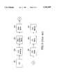
- FIG. 1is a schematic diagram showing the idea of pixel insertion.
- the small squaresrepresent original pixels of the image which have CCD (Charged Couple Device) resolution of 600 dpi.
- CCDCharge Couple Device
- the small triangles which also have CCD resolution of 600 dpirepresent the pixels inserted to the original image to enhance the resolution of the original image. Consequently, after pixel insertion, the final resolution is increased to 1200 dpi.
- pixel insertioncan be accomplished using either software or hardware.
- the software implementationis commonly called "interpolation”.
- Software implementationis cheaper than hardware implementation.
- the implementationis also much easier. However, it is very slow.
- FIG. 2is a schematic diagram of the structure of a scanner.
- CCD 201senses the image and then sends the analog sisal to A/D converter 202 to be converted into digital data.
- the digital datais then forwarded to interpolation device 203 for pixel insertion.
- the image datais stored in video buffer 204.
- Video buffer 204can be a DRAM or a SRAM.
- FIFO device 205is for increasing the transmission rate of I/O device 206.
- I/O device 206can be a SCSI connector, printer port, or any other devices which can be used as an I/O device.
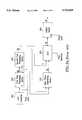
- FIG. 3Ashows the operations performed in the devices corresponding to the devices of FIG. 2.
- A/D converter 301outputs pixels to first pixel processing device 302 in sequential order.
- First pixel processing device 302 and second pixel processing device 303are both latch devices. The difference is that first pixel processing device 302 processes the nth pixel while second pixel processing device 303 processes the (n-1)th pixel.
- Mean value generating device 304generates the mean value of the outputs of the first pixel processing device 302 and second pixel processing device 303. That is, the value of (QA+QB)/2.
- mean value generating device 304is for computing the interpolation value of the pixels.
- a MUX 305is for selecting the output (QB)of second pixel processing device 303 or the output (QC)of mean value generating device 304. The output of MUX 305 is then sent to output device 306.
- the timing diagramconsists of stages.
- Q nis the value of the nth pixels.
- the data for QAis Q n .
- the data for QBis Q n-1 .
- the data for QCis (Q n-1 +Q n )/2.
- the data for QEis (Q n-2 +Q n-1 )/2.
- first pixel processing device 302, second pixel processing device 303, mean value generating device 304, MUX 305, and output device 306are processed synchronously.
- the present inventionencompasses: a video buffer for storing scanned image data; an input buffer for receiving the scanned image data from the video buffer and forwarding the scanned image data to an interpolation device; an interpolation device for inserting pixels into the the pixels of original image data; and an output buffer for outputting the pixels of the image data from the interpolation device to an I/O device.
- FIG. 1is a diagram showing a pixel insertion method.
- FIG. 2is a block diagram showing the structure of a pixel insertion apparatus in a scanner according to the prior an.
- FIG. 3Ais a block diagram showing the operation of inserting pixels according to the prior art.
- FIG. 3Bis a timing diagram of FIG. 3A.
- FIG. 4is a block diagram showing the preferred embodiment of the invention.
- FIG. 5is a block diagram showing the preferred embodiment of the invention.
- FIG. 4is a block diagram showing the arrangement and order of the invention in a scanner.
- CCD 401is for capturing the image data which are output as analog signals.
- A/D converter 402converts the analog image data input to digital signals.
- Video buffer 403stores digital image data and then forwards the image data to interpolation device 404 for pixel insertion. After the interpolation process is complete.
- the image datais sent to I/O device 405 for transmitting the data to a host machine or displaying device 406.
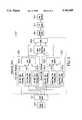
- Input buffer 501receives the output of video buffer 500, then forwards the scanned image data to interpolation device 502 for pixel insertion. Interpolation device 502 inserts pixels into the original pixels. After the interpolation process is complete, output buffer 503 forwards the image data to I/O device 504.
- the interpolation device 502mainly contains four parts: (1) first pixel processing device 5021 which processes odd number pixels of various colors; (2) second pixel processing device 5022 which processes even number pixels of various colors; (3) mean values generating device 5023 for generating mean value of the outputs of first pixel processing device 5021 and second pixel processing device 5022; (4) MUX 5024 for selecting an output of the first pixel processing device 5021, second pixel processing device 5022 and mean value generating device 5023.
- First pixel processing device 5021contains: first red color processing device 50211 for processing red color ingredients of pixels; first green color processing device 50212 for processing green color ingredients of pixels; first blue color processing device 50213 for processing blue color ingredients of pixels; and first color selector 50214 for selecting an output of first red color processing means, first green color processing device, and blue color processing device.
- First color selector 50214can be a multiplexer or equivalent device.
- Second pixel processing device 5022contains similar devices to that of first pixel processing device 5021. The difference is only that second pixel processing device 5022 processes only pixels of even number. As the figure shows, second red color processing device 50221 processes red color data for the even number pixels. Second green color processing device 50222 processes green color ingredients of pixels. Second blue color processing device 50223 processes blue color ingredients of pixels. And second color selector 50224 is for selecting an output of red color processing means, green color processing means, and blue color processing means. Second color selector 50224 can also be a multiplexer or any equivalent device.
- Mean value generating device 5023receives the output values of first pixel processing device 5021 and second pixel processing device 5022 and then generates a mean value of their output value.
- the function of mean value generating device 5023is the same as that of prior art.
- MUX 5024is for selecting the output of first pixel processing device 5021, second pixel processing device 5022, or mean value generating device 5023. When MUX 5024 is enabled, the desired output will be sent to output buffer 503. When the host machine 505 is requesting image data, I/O device 504 forwards the data in output buffer 503 to host machine 505 to display the scanned image.
- the inventionrelocates the position of interpolation device 404 at the position after video buffer 403.
- the size of the video buffer 403 and bandwidthremains the same without having to fit the size of the enlarged image data.
- the inventiondoes not need a FIFO device as in the prior art because the image data to be transmitted to the host machine or displaying device 406 is already in interpolation device 404. It does not have to wait for the video buffer 403 to get ready to transfer.
- the interpolation device 502performs also as a FIFO device. Because of these alterations, the invention can improve the transmission rate between the I/O device 504 and the displaying device 505.
- input buffer 501sends image data to first or second pixel processing devices.
- MUX 5024selects original pixels or inserted pixels of desired colors and then latches the data.
Landscapes
- Engineering & Computer Science (AREA)
- Multimedia (AREA)
- Signal Processing (AREA)
- Image Input (AREA)
- Image Processing (AREA)
Abstract
Description
Claims (16)
Priority Applications (1)
| Application Number | Priority Date | Filing Date | Title |
|---|---|---|---|
| US08/544,483US5742409A (en) | 1995-10-18 | 1995-10-18 | Apparatus for pixel insertion in optical scanners |
Applications Claiming Priority (1)
| Application Number | Priority Date | Filing Date | Title |
|---|---|---|---|
| US08/544,483US5742409A (en) | 1995-10-18 | 1995-10-18 | Apparatus for pixel insertion in optical scanners |
Publications (1)
| Publication Number | Publication Date |
|---|---|
| US5742409Atrue US5742409A (en) | 1998-04-21 |
Family
ID=24172365
Family Applications (1)
| Application Number | Title | Priority Date | Filing Date |
|---|---|---|---|
| US08/544,483Expired - LifetimeUS5742409A (en) | 1995-10-18 | 1995-10-18 | Apparatus for pixel insertion in optical scanners |
Country Status (1)
| Country | Link |
|---|---|
| US (1) | US5742409A (en) |
Cited By (7)
| Publication number | Priority date | Publication date | Assignee | Title |
|---|---|---|---|---|
| US6362847B1 (en) | 1999-06-15 | 2002-03-26 | Lexmark International, Inc. | Electronic control arrangement for a laser printer |
| US20020145765A1 (en)* | 2001-04-04 | 2002-10-10 | Chou Huil-Ing | Method and apparatus for increasing scan resolution |
| US6542260B1 (en)* | 1997-01-13 | 2003-04-01 | Hewlett-Packard Company | Multiple image scanner |
| US6809843B1 (en)* | 1999-06-30 | 2004-10-26 | Hewlett-Packard Development Company, L.P. | Virtual whiteboard |
| US6958826B1 (en)* | 1999-05-25 | 2005-10-25 | Silverbrook Research Pty Ltd | Controller for a printer module |
| US20100074559A1 (en)* | 2008-09-24 | 2010-03-25 | Oki Semiconductor Co., Ltd. | Device for interpolating image |
| US10228890B2 (en) | 2014-06-13 | 2019-03-12 | Canon Kabushiki Kaisha | Apparatus, method, and non-transitory computer-readable storage medium |
Citations (7)
| Publication number | Priority date | Publication date | Assignee | Title |
|---|---|---|---|---|
| US4611348A (en)* | 1984-11-26 | 1986-09-09 | General Electric Company | Apparatus for altering the spatial characteristics of a digital image by polynomial interpretation using sets of arithmetic processors |
| US4712141A (en)* | 1985-03-30 | 1987-12-08 | Dainippon Screen Mfg. Co., Ltd. | Method and apparatus for interpolating image signals |
| US4734759A (en)* | 1985-05-09 | 1988-03-29 | Hitachi, Ltd. | A video printer having color signal interpolation circuit |
| US4740832A (en)* | 1986-10-14 | 1988-04-26 | Technology, Inc., 64 | Image storage using separately scanned luminance and chrominance variables |
| US4783698A (en)* | 1987-04-13 | 1988-11-08 | Technology Inc., 64 | Interpolator for compressed video data |
| US4796085A (en)* | 1986-02-18 | 1989-01-03 | Fuji Photo Film Co., Ltd. | Device for interpolating missing color-difference signal by averaging line-sequential color-difference signals |
| US5646696A (en)* | 1992-12-23 | 1997-07-08 | Intel Corporation | Continuously changing image scaling performed by incremented pixel interpolation |
- 1995
- 1995-10-18USUS08/544,483patent/US5742409A/ennot_activeExpired - Lifetime
Patent Citations (7)
| Publication number | Priority date | Publication date | Assignee | Title |
|---|---|---|---|---|
| US4611348A (en)* | 1984-11-26 | 1986-09-09 | General Electric Company | Apparatus for altering the spatial characteristics of a digital image by polynomial interpretation using sets of arithmetic processors |
| US4712141A (en)* | 1985-03-30 | 1987-12-08 | Dainippon Screen Mfg. Co., Ltd. | Method and apparatus for interpolating image signals |
| US4734759A (en)* | 1985-05-09 | 1988-03-29 | Hitachi, Ltd. | A video printer having color signal interpolation circuit |
| US4796085A (en)* | 1986-02-18 | 1989-01-03 | Fuji Photo Film Co., Ltd. | Device for interpolating missing color-difference signal by averaging line-sequential color-difference signals |
| US4740832A (en)* | 1986-10-14 | 1988-04-26 | Technology, Inc., 64 | Image storage using separately scanned luminance and chrominance variables |
| US4783698A (en)* | 1987-04-13 | 1988-11-08 | Technology Inc., 64 | Interpolator for compressed video data |
| US5646696A (en)* | 1992-12-23 | 1997-07-08 | Intel Corporation | Continuously changing image scaling performed by incremented pixel interpolation |
Cited By (8)
| Publication number | Priority date | Publication date | Assignee | Title |
|---|---|---|---|---|
| US6542260B1 (en)* | 1997-01-13 | 2003-04-01 | Hewlett-Packard Company | Multiple image scanner |
| US6958826B1 (en)* | 1999-05-25 | 2005-10-25 | Silverbrook Research Pty Ltd | Controller for a printer module |
| US6362847B1 (en) | 1999-06-15 | 2002-03-26 | Lexmark International, Inc. | Electronic control arrangement for a laser printer |
| US6650352B2 (en) | 1999-06-15 | 2003-11-18 | Lexmark International, Inc. | Electronic control arrangement for a laser printer |
| US6809843B1 (en)* | 1999-06-30 | 2004-10-26 | Hewlett-Packard Development Company, L.P. | Virtual whiteboard |
| US20020145765A1 (en)* | 2001-04-04 | 2002-10-10 | Chou Huil-Ing | Method and apparatus for increasing scan resolution |
| US20100074559A1 (en)* | 2008-09-24 | 2010-03-25 | Oki Semiconductor Co., Ltd. | Device for interpolating image |
| US10228890B2 (en) | 2014-06-13 | 2019-03-12 | Canon Kabushiki Kaisha | Apparatus, method, and non-transitory computer-readable storage medium |
Similar Documents
| Publication | Publication Date | Title |
|---|---|---|
| US4386367A (en) | System and method for converting a non-interlaced video signal into an interlaced video signal | |
| US5402248A (en) | Image encoding apparatus and method | |
| US5068905A (en) | Scaler gate array for scaling image data | |
| US5982425A (en) | Method and apparatus for draining video data from a planarized video buffer | |
| US6307974B1 (en) | Image processing apparatus, system, and method with adaptive transfer | |
| US5742409A (en) | Apparatus for pixel insertion in optical scanners | |
| US4799110A (en) | Image signal coding apparatus | |
| CA2218988A1 (en) | Low cost digital scanners | |
| EP0205712A2 (en) | Video stream processing system | |
| US20010048628A1 (en) | Method of controlling line memory | |
| US20020054711A1 (en) | Method for transmitting image data of a scanner | |
| JP3116989B2 (en) | Decompression device for compressed binary image data | |
| EP0558292B1 (en) | Compression/expansion circuit | |
| JP4132264B2 (en) | Image signal processing circuit | |
| JP3028096B2 (en) | Image data transfer system and method | |
| JP3225658B2 (en) | Image information processing device | |
| JPH03102955A (en) | Picture reader | |
| JP3189873B2 (en) | Color converter | |
| US20060103896A1 (en) | Duplex scan apparatus | |
| JP3426697B2 (en) | Image format converter | |
| JPS61198872A (en) | Picture input device | |
| WO1999018719A1 (en) | Method of and apparatus for transmitting scaled and compressed raw ccd video data from a video camera | |
| US20050025385A1 (en) | Image processing device and method therefor | |
| TW569616B (en) | Method for compressing an image in real time and shading compressing an images | |
| JP2641432B2 (en) | Interface device |
Legal Events
| Date | Code | Title | Description |
|---|---|---|---|
| AS | Assignment | Owner name:UMAX DATA SYSTEM INC., TAIWAN Free format text:ASSIGNMENT OF ASSIGNORS INTEREST;ASSIGNORS:TSAI, CHA-LIN;HONG, ALECK;REEL/FRAME:007738/0521 Effective date:19950510 | |
| STCF | Information on status: patent grant | Free format text:PATENTED CASE | |
| FPAY | Fee payment | Year of fee payment:4 | |
| FPAY | Fee payment | Year of fee payment:8 | |
| AS | Assignment | Owner name:VEUTRON CORPORATION, TAIWAN Free format text:CHANGE OF NAME;ASSIGNOR:UMAX DATA SYSTEMS INC.;REEL/FRAME:016800/0203 Effective date:20021029 | |
| AS | Assignment | Owner name:TRANSPACIFIC IP, LTD.,TAIWAN Free format text:ASSIGNMENT OF ASSIGNORS INTEREST;ASSIGNOR:VEUTRON CORPORATION;REEL/FRAME:017564/0747 Effective date:20050706 Owner name:TRANSPACIFIC IP, LTD., TAIWAN Free format text:ASSIGNMENT OF ASSIGNORS INTEREST;ASSIGNOR:VEUTRON CORPORATION;REEL/FRAME:017564/0747 Effective date:20050706 | |
| AS | Assignment | Owner name:TRANSPACIFIC SYSTEMS, LLC, DELAWARE Free format text:ASSIGNMENT OF ASSIGNORS INTEREST;ASSIGNOR:TRANSPACIFIC IP LTD.;REEL/FRAME:023107/0267 Effective date:20090618 Owner name:TRANSPACIFIC SYSTEMS, LLC,DELAWARE Free format text:ASSIGNMENT OF ASSIGNORS INTEREST;ASSIGNOR:TRANSPACIFIC IP LTD.;REEL/FRAME:023107/0267 Effective date:20090618 | |
| FPAY | Fee payment | Year of fee payment:12 | |
| AS | Assignment | Owner name:TITUSVILLE CANAVERAL LLC, DELAWARE Free format text:MERGER;ASSIGNOR:TRANSPACIFIC SYSTEMS, LLC;REEL/FRAME:030628/0681 Effective date:20130213 | |
| AS | Assignment | Owner name:INTELLECTUAL VENTURES I LLC, DELAWARE Free format text:MERGER;ASSIGNOR:TITUSVILLE CANAVERAL LLC;REEL/FRAME:030639/0330 Effective date:20130214 |