US5740013A - Electronic device enclosure having electromagnetic energy containment and heat removal characteristics - Google Patents
Electronic device enclosure having electromagnetic energy containment and heat removal characteristicsDownload PDFInfo
- Publication number
- US5740013A US5740013AUS08/676,602US67660296AUS5740013AUS 5740013 AUS5740013 AUS 5740013AUS 67660296 AUS67660296 AUS 67660296AUS 5740013 AUS5740013 AUS 5740013A
- Authority
- US
- United States
- Prior art keywords
- enclosure
- enclosure portion
- contact
- printed circuit
- circuit board
- Prior art date
- Legal status (The legal status is an assumption and is not a legal conclusion. Google has not performed a legal analysis and makes no representation as to the accuracy of the status listed.)
- Expired - Lifetime
Links
Images


Classifications
- H—ELECTRICITY
- H05—ELECTRIC TECHNIQUES NOT OTHERWISE PROVIDED FOR
- H05K—PRINTED CIRCUITS; CASINGS OR CONSTRUCTIONAL DETAILS OF ELECTRIC APPARATUS; MANUFACTURE OF ASSEMBLAGES OF ELECTRICAL COMPONENTS
- H05K9/00—Screening of apparatus or components against electric or magnetic fields
- H05K9/0007—Casings
- H05K9/002—Casings with localised screening
- H05K9/0022—Casings with localised screening of components mounted on printed circuit boards [PCB]
- H05K9/0024—Shield cases mounted on a PCB, e.g. cans or caps or conformal shields
- H05K9/0032—Shield cases mounted on a PCB, e.g. cans or caps or conformal shields having multiple parts, e.g. frames mating with lids
- H05K9/0033—Shield cases mounted on a PCB, e.g. cans or caps or conformal shields having multiple parts, e.g. frames mating with lids disposed on both PCB faces
- H—ELECTRICITY
- H01—ELECTRIC ELEMENTS
- H01L—SEMICONDUCTOR DEVICES NOT COVERED BY CLASS H10
- H01L23/00—Details of semiconductor or other solid state devices
- H01L23/34—Arrangements for cooling, heating, ventilating or temperature compensation ; Temperature sensing arrangements
- H01L23/46—Arrangements for cooling, heating, ventilating or temperature compensation ; Temperature sensing arrangements involving the transfer of heat by flowing fluids
- H01L23/467—Arrangements for cooling, heating, ventilating or temperature compensation ; Temperature sensing arrangements involving the transfer of heat by flowing fluids by flowing gases, e.g. air
- H—ELECTRICITY
- H01—ELECTRIC ELEMENTS
- H01L—SEMICONDUCTOR DEVICES NOT COVERED BY CLASS H10
- H01L2924/00—Indexing scheme for arrangements or methods for connecting or disconnecting semiconductor or solid-state bodies as covered by H01L24/00
- H01L2924/0001—Technical content checked by a classifier
- H01L2924/0002—Not covered by any one of groups H01L24/00, H01L24/00 and H01L2224/00
Definitions
- the present inventionrelates generally to electronic device enclosures and, more particularly, to electronic device enclosures having the ability to contain electromagnetic energy and remove heat generated by electronic devices during operation.
- a typical computermay, for example, include a relatively large central processing unit which may be surrounded by a plurality of secondary electronic components such as cache SRAM memory devices. Both the central processing unit and the secondary components are generally constructed as integrated circuit devices which are mounted on a printed circuit board.
- Integrated circuit devicesinherently emit electromagnetic radiation during operation. This electromagnetic radiation may cause interference with communication devices, such as telephones, radios, and televisions. As the power and sophistication of integrated circuit devices have increased, so has the level of electromagnetic interference generated by such devices.
- both the central processing unit and the secondary electronic componentsmay be encased in an electrically conductive enclosure in order to block the emission of electromagnetic radiation.
- integrated circuit devicesDuring normal operation, integrated circuit devices also generate significant amounts of heat. If this heat is not continuously removed, the integrated circuit device may overheat, resulting in damage to the device and/or a reduction in operating performance. Along with an increase in electromagnetic radiation, the increased power and sophistication of integrated circuit devices over the years has also resulted in an increase in heat generated by the devices and, thus, increases the difficulty of cooling the devices.
- integrated circuit cooling devicesare often used in conjunction with integrated circuit devices.
- a cooling deviceis a fan assisted heat sink cooling device.
- a heat sinkis formed of a material, such as aluminum, which readily conducts heat.
- the heat sinkis usually placed on top of and in contact with the integrated circuit device. Due to this contact, heat generated by the integrated circuit is conducted into the heat sink and away from the integrated circuit.
- the heat sinkmay include a plurality of cooling fins in order to increase the surface area of the heat sink and, thus, maximize the transfer of heat from the heat sink into the surrounding air. In this manner, the heat sink is able to draw heat away from the integrated circuit and transfer the heat into the surrounding air.
- an electrically powered fanis often mounted in proximity to the heat sink.
- the fancauses air to move over and around the fins of the heat sink device, thus cooling the fins by enhancing the transfer of heat from the fins into the ambient air.
- an electromagnetic containment enclosurein a manner as previously described, interferes with the ability of an integrated circuit cooling device, such as a fan assisted cooling device, to adequately cool the integrated circuit device located within the containment enclosure.
- an integrated circuit cooling devicesuch as a fan assisted cooling device
- the electromagnetic containment enclosuremust completely surround the integrated circuit device, however, the cooling device would have to be located within the electromagnetic enclosure in order to be in contact with the electronic circuit device being cooled. Locating the cooling device within the enclosure in this manner would interfere with the ability of the cooling device to transfer heat into the surrounding air and, thus, would prevent the cooling device from efficiently cooling the electronic component.
- the mounting mechanisms for integrated circuit devicesoften interfere with the optimum operation of integrated circuit cooling devices.
- the mounting arrangement of many integrated circuit devicese.g., a central processing unit of a computer, requires that the integrated circuit device be clamped to the printed circuit board with a certain level of force.
- clamping mechanismsare generally provided which contact the top of the integrated circuit device and thereby clamp the integrated circuit device to the printed circuit board. The location of such clamping mechanisms often prevents a cooling device from directly contacting the integrated circuit device and, thus, prevents the cooling device from properly cooling the integrated circuit device.
- the present inventionis directed to an enclosure for integrated circuit devices.
- the enclosuremay include a first part which substantially encloses a plurality of relatively low-power secondary integrated circuit devices mounted on a pc board.
- the enclosure first partmay include a mechanism for contacting the secondary integrated circuit devices in order to conduct heat away from the secondary devices and thus cool the devices.
- the enclosure first partmay be provided with cooling fins to facilitate this cooling function.
- the enclosuremay also include a second part which may include an active cooling device which is directly in contact with a relatively high-power primary integrated circuit device mounted on the pc board.
- the active cooling deviceserves to cool the primary integrated circuit device.
- the enclosure first partmay be configured to allow a first level of controlled force to be applied to the secondary integrated circuit devices.
- the enclosure second partmay be configured to allow a second level of controlled force, independent of the first level of controlled force, to be applied to the primary integrated circuit device.
- the first and second enclosure partsmay, together, completely enclose the primary and secondary integrated circuit devices and may be electrically interconnected such that the enclosure also serves to block electromagnetic energy generated by the devices from escaping from the enclosure.
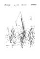
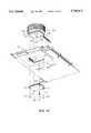
- FIG. 1is a top exploded perspective view showing the attachment of top and bottom enclosure portions to a pc board.
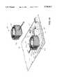
- FIG. 2is a bottom exploded perspective view showing the attachment of FIG. 1.
- FIG. 3is a top plan view of an upper enclosure portion.
- FIG. 4is a bottom plan view of the upper enclosure portion of FIG. 3.
- FIG. 5is a cross-sectional view of the upper enclosure portion taken along the line 5--5 of FIG. 3.
- FIG. 6is a bottom perspective view of a cooling device used in conjunction with the upper enclosure portion of FIG. 3.
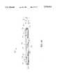
- FIG. 7is a top perspective view of a fully assembled enclosure mounted on a pc board.
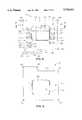
- FIG. 8is top plan view of a lower enclosure portion.
- FIG. 9is a bottom plan view of the lower enclosure portion of FIG. 8.
- FIG. 10is a cross-sectional view of the lower enclosure portion taken along the line 10--10 of FIG. 8.
- FIG. 11is a bottom perspective view of a bolster plate used in conjunction with the lower enclosure portion of FIG. 8.
- FIG. 12is a bottom perspective view of a fully assembled enclosure mounted on a pc board.
- FIG. 13is a bottom exploded perspective view showing the attachment of the cooling device of FIG. 6 to the upper enclosure portion of FIG. 3 and the attachment of the bolster plate of FIG. 11 to the lower enclosure portion of FIG. 8.
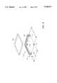
- FIG. 14is a top perspective view of an enclosure having two cooling devices mounted thereon.
- FIGS. 1-14in general, illustrate an enclosure mounted on a printed circuit board 10 in proximity to at least one primary integrated circuit device 12 and at least one secondary electronic component 14 which are mounted on the printed circuit board 10.
- the enclosureincludes a first enclosure portion 100 including an upper wall member 102 extending substantially parallel to the printed circuit board 10, wherein the upper wall member 102 has a lower surface 106 facing the printed circuit board 10, an upper surface 104 opposite the lower surface 106 and at least one opening 136 therein located proximate the at least one primary integrated circuit device 12; a plurality of leg wall members 108, 110, 112, 114, 116, 118 extending transversely from the upper wall member 102 toward an upper surface 38 of the printed circuit board 10; at least one contact member 142 extending from the upper wall member lower surface 106 toward the printed circuit board upper surface 38, wherein the at least one contact member 142 is in contact with the at least one secondary component 14.
- the enclosuremay also include at least one cooling device 250 having a lower surface 278 in contact with the at least one primary integrated circuit device 12; and wherein the at least one cooling device 250 is located within the at least one first enclosure portion opening 136 and is in electrical contact with the first enclosure portion 100.
- FIGS. 1-14also illustrate, in general, an enclosure mounted on a printed circuit board 10 in proximity to at least one primary integrated circuit device 12 mounted on the printed circuit board 10.
- the enclosuremay include a first enclosure portion 100 in contact with an upper surface 38 of the printed circuit board 10 and including at least one opening 136 therein located proximate the at least one primary integrated circuit device 12; at least one cooling device 250 in contact with the at least one primary integrated circuit device 12; and wherein at least a portion of the at least one cooling device 250 is located within the at least one first enclosure portion opening 136 and is in electrical contact with the first enclosure portion 100.
- FIGS. 1-14also illustrate, in general, a method of enclosing at least one primary integrated circuit device 12 and at least one secondary electronic component 14 which are mounted on a printed circuit board 10.
- the methodmay include the steps of providing a first enclosure portion 100 having at least one opening 136 located therein; mounting the first enclosure portion on a first surface 38 of the printed circuit board 10 and contacting the at least one secondary component 14 with the first enclosure portion 100 to apply a first level of force to the at least one secondary component 14; providing at least one cooling device 250; placing at least a part of the at least one cooling device 250 within the at least one first enclosure portion opening 136 and contacting the at least one primary integrated circuit device 12 with the at least a part of the at least one cooling device 250 to apply a second level of force to the at least one primary integrated circuit device 12; and establishing electrical contact between the at least one cooling device 250 and the first enclosure portion 100.
- FIG. 1illustrates a printed circuit board 10.
- a primary integrated circuit device 12may be mounted on an upper surface 38 of the printed circuit bard 10 as shown.
- Primary integrated circuit device 12may be a central processing unit for a computer and may, for example, be a central processing unit of the type commercially available from Hewlett-Packard Company and sold as a "PA-7200" processor.
- Surrounding the primary integrated circuit device 12are a plurality of secondary integrated circuit devices 14, such as the individual secondary integrated circuit devices 16, 18, 20, 22, 24, 26, 28, 30, 32, 34 and 36.
- Secondary integrated circuit devices 14may, for example, be cache SRAM memory devices. Referring to FIG. 2, it can be seen that some of the secondary integrated circuit devices 14, e.g., the secondary devices 16, 18, 20, 22, 24, 30, 32, 34 and 36, may extend completely through the pc board 10 and project from the bottom surface 40 of the pc board 10.
- PC board 10may include other electronic components, schematically illustrated by reference numeral 42 in FIG. 1, and a connection device 44 in a conventional manner.
- Connection device 44may be provided to allow the integrated circuit devices located on the pc board 10 to interface with electronic components located elsewhere. In the case of a computer, for example, the connection device 44 may allow the pc board to communicate with such user interface devices as a monitor and a keyboard.
- Integrated circuit devicessuch as the primary integrated circuit device 12 and the secondary integrated circuit devices 14, inherently emit electromagnetic radiation during operation. This electromagnetic radiation may cause interference with communication devices, such as telephones, radios, and televisions. It is, therefore, desirable to block this radiation to prevent such interference.
- integrated circuit devicessuch as the primary integrated circuit device 12 and the secondary integrated circuit devices 14, typically generate significant amounts of heat during operation. In order to prevent damage to and/or reduced efficiency of the integrated circuit devices, it is necessary to remove this heat by cooling the devices during operation. This is particularly true with respect to the primary integrated circuit device because this device tends to draw more power and, thus, generate more heat than do the secondary integrated circuit devices 14.
- the enclosuremay generally include an upper enclosure portion 100 which is adapted to contact the upper surface 38 of the pc board 10, FIG. 1, and a lower enclosure portion 300 which is adapted to contact the lower surface 40 of the pc board 10, FIG. 2.
- Upper enclosure portion 100may be generally formed from a substantially planar top wall member 102 which may include an upper surface 104, FIG. 3 and a lower surface 106, FIG. 4. Extending transversely downwardly from the top wall member 102 are a plurality of side wall members 108, 110, 112, 114, 116 and 118, FIGS. 2 and 4. The side wall members 108, 110, 112, 114, 116 and 118 may be integrally formed with the top wall member 102. Each of the side wall members may include a downwardly facing end portion 120, 122, 124, 126, 128 and 130, respectively. Upper enclosure portion 100 may have an overall height "o" of about 11.2 mm, FIG. 5.
- a first and second set of cooling fins 132, 134may extend upwardly from the top wall member upper surface 104. Each of the fins may extend a distance "a" of about 15 mm above the top wall member upper surface 104, FIG. 5.
- An opening 136may be provided in the top wall member 102 as shown. Referring to FIGS. 4 and 5, it can be seen that the opening 136 may be surrounded by a flange portion 138. The flange portion 138 may be integrally formed with the top wall member 102 and may extend a distance "b" of about 6.9 mm below the top wall member upper surface 104, FIG. 5.
- the opening 136may be substantially rectangular and have a length "d" of about 65.6 mm and a width "e” of about 54.7 mm.
- a beveled surface 140may be provided between the top wall member upper surface 104 and the opening flange 138 as shown.
- a plurality of bosses 142such as the individual bosses 146, 148, 150, 152, 154, 156, 158, 160, 162, 164 and 166 may extend downwardly from the top wall member lower surface 106 as shown.
- the bosses 142may be integrally formed with the top wall member 102 and may extend for the distance "b" of about 6.9 mm below the top wall member upper surface 104, FIG. 5.
- the bosses 142may be have a generally rectangular cross-section as shown and may be sized and arranged to correspond to the size and arrangement of the secondary integrated circuit devices 14 located on the pc board 10, FIG. 1.
- each bossmay be provided with a series of slots, such as the slots 168, 170, 172 in the boss 154.
- compliant thermal interface pads 174may be attached to each of the bosses 142 as shown, for example, with respect to the compliant thermal interface pads 176, 178, 180 attached to the bosses 156, 158, 160, respectively.
- the interface pads 174will be compressed between the bosses 142 and the respective secondary integrated circuit devices 14. In this manner, the interface pads 174 assist in conducting heat from the secondary integrated circuit devices through the bosses 142 and into the remainder of the upper enclosure portion 100 as will be explained in more detail herein.
- Compliant thermal interface pads 174may each have a thickness of approximately 0.125 inches and may be sized and shaped to correspond generally to the size and shape of the bosses 142.
- the compliant thermal interface pads 174may be made of a material commercially available from Bergquist Company of Minneapolis, Minn. and sold as "Gap Pad" thermal interface sheet.
- Upper enclosure portion 100may be provided with a plurality of through-holes 182, 184, 186, 188 and 190 as shown, for example, in FIGS. 3 and 4. These holes may align with a plurality of holes 52, 54, 56, 58 and 60, respectively, located in the pc board 10, FIG. 1, to facilitate mounting of the upper enclosure portion 100 on the pc board 10 as will be explained in further detail herein.
- Upper enclosure portion 100may be formed of a material which is both electrically conductive and which readily conducts heat. In this manner, upper enclosure portion 100 may serve to both conduct heat away from the secondary integrated circuit devices 14 and to contain electromagnetic energy generated by the integrated circuit devices 12 and 14 as will be explained in further detail herein.
- Upper enclosure portion 100may, for example, be formed of aluminum generally having a thickness of about 3 mm.
- resilient contact fingers 192may be extend downwardly from each of the side wall member end portions 120, 122, 124, 126, 128 and 130.
- the fingers 192are adapted to contact a metallized ground pad 62 located on the upper surface 38 of the pc board 10, FIG. 1, when the upper enclosure portion 100 is mounted on the pc board 10. This contact between the fingers 192 and the ground pad 62 facilitates electrical contact between the upper enclosure portion 100 and the pc board ground and, thus, enhances the ability of the upper enclosure portion 10 to contain electromagnetic interference generated by the integrated circuit devices 12 and 14, as will be explained in more detail herein.
- the fingers 192may be integrally formed with a leg member 194 which may be adhered to the inside surface of the side wall portions 108, 110, 112, 114, 116 and 118 in a conventional manner.
- the contact fingers 192may be of the type commercially available from Instrument Specialties Co. of Delaware Water Gap, Pa. and sold as "Sticky Fingers" EMI gasketing material. It is noted that, for purposes of clarity, the contact fingers 192 are not shown in FIG. 4.
- a cooling device 250may be provided as shown. Cooling device 250 may generally be constructed having a heat sink portion 252 and a fan 254 located within the heat sink portion 252, FIG. 7. Cooling device 250 may be of the type disclosed in the previously referenced U.S. patent application Ser. No. 08/593,185 or may, alternatively, be any conventional type of cooling device used to remove heat from electronic components. In order to facilitate containment of electromagnetic radiation from the integrated circuit devices 12 and 14, as will be explained in more detail herein, the heat sink portion 252 should be constructed of an electrically conductive material such as aluminum. A power cable 260 may be provided as shown in order to deliver electrical energy to the fan 254 located within the heat sink 252 in a conventional manner.
- a pedestal 256may extend from a lower surface 258 of the cooling device heat sink portion 252.
- the pedestal 256may be integrally formed with the heat sink 252 and may be generally rectangular, having a length "f" of about 64.6 mm and a width "g" of about 53.7 mm.
- the pedestal 256may extend a distance of about 7 mm below the heat sink lower surface 258 and may include a lower surface 278 as shown.
- a groove 262may be provided around a lower portion of the pedestal 256 as shown.
- An electrically conductive, compressible O-ring 264may be provided as shown, and may be sized to fit securely within the groove 262 in a conventional manner.
- O-ring 264may be in the form of a metallic spring and may be of the type commercially available from Bal Seal Engineering Company of Santa Ana, Calif. and sold as part no. 105LB.
- the pedestal 256may be provided with a plurality of threaded holes 266, 268, 270 and 272 and with a pair of non-threaded holes 274 and 276 as shown.
- the cooling device pedestal 256When the cooling device 250 is mounted on the upper enclosure portion 100, as shown in FIG. 7, the cooling device pedestal 256 fits within the upper enclosure portion opening 136. When so mounted, the compressible O-ring 264 will be compressed between the pedestal groove 262 and the upper enclosure portion flange 138, FIGS. 1 and 5. The contact between the upper enclosure portion flange 138, the conductive O-ring 264 and the cooling device pedestal groove 262 facilitates electrical contact between the upper enclosure portion 100 and the cooling device 250 and, thus, enhances the ability of the upper enclosure portion 100 and attached cooling device 250 to contain electromagnetic interference generated by the integrated circuit devices 12 and 14, as will be explained in more detail herein. When inserting the cooling device pedestal 256 into the upper enclosure portion opening 136, the beveled surface 140, FIG. 3, facilitates compression of the compressible O-ring 264.
- lower enclosure portion 300may be generally formed from a substantially planar bottom wall member 302 which may include an upper surface 304, FIG. 8 and a lower surface 306, FIG. 9. Extending transversely upwardly from the bottom wall member 302 are a plurality of side wall members 308, 310, 312, 314, 316 and 318, FIGS. 1 and 8.
- the side wall members 308, 310, 312, 314, 316 and 318may be integrally formed with the bottom wall member 302.
- Each of the side wall membersmay include an upwardly facing end portion 320, 322, 324, 326, 328 and 330, respectively.
- Lower enclosure portion 300may have an overall height "p" of about 7.9 mm, FIG. 10.
- an opening 336may be provided in the bottom wall member 302 as shown.
- the opening 336may be surrounded by a flange portion 338.
- the flange portion 338may be integrally formed with the bottom wall member 302 and may extend a distance "h" of about 3.7 mm above the bottom wall member lower surface 306, FIG. 10.
- the hole 336may be substantially rectangular and have a length "j" of about 65.6 mm and a width "k” of about 54.7 mm.
- a beveled surface 340, FIG. 9,may be provided between the bottom wall member lower surface 306 and the opening flange 338 as shown.
- a plurality of bosses 342such as the individual bosses 346, 348, 350, 352, 354, 360, 362, 364 and 366 may extend upwardly from the bottom wall member upper surface 304 as shown.
- the bosses 342may be integrally formed with the bottom wall member 302 and may extend for a distance "i" of about 3.6 mm above the bottom wall member lower surface 304, FIG. 10.
- the bosses 342may be have a generally rectangular cross-section as shown and may be sized and arranged to correspond to the size and arrangement of the secondary integrated circuit devices 14 located on the pc board 10, FIG. 2.
- each boss 42may be provided with a series of slots, such as the slots 368, 370, 372 in the boss 354.
- compliant thermal interface pads 74may be attached to each of the bosses 342 as shown, for example, with respect to the compliant thermal interface pads 376, 378, 380 attached to the bosses 362, 364, 366, respectively.
- the interface pads 374will be compressed between the bosses 342 and the respective secondary integrated circuit devices 14. In this manner, the interface pads 374 assist in conducting heat from the secondary integrated circuit devices through the bosses 342 and into the remainder of the lower enclosure portion 300 as will be explained in more detail herein.
- the compliant thermal interface pads 374may each have a thickness of approximately 0.125 inches and may be sized and shaped to correspond generally to the size and shape of the bosses 342.
- the compliant thermal interface pads 374may be identical to the thermal interface pads 174, previously described.
- Lower enclosure portion 300may be provided with a plurality of threaded holes 382, 384, 386, 388 and 390 as shown, for example, in FIGS. 8 and 9. These holes may align with the plurality of holes 52, 54, 56, 58 and 60, respectively, located in the pc board 10, FIG. 1, to facilitate mounting of the lower enclosure portion 300 on the pc board 10 as will be explained in further detail herein.
- Lower enclosure portion 300may be formed of a material which is both electrically conductive and which readily conducts heat. In this manner, lower enclosure portion 300 may serve to both conduct heat away from the secondary integrated circuit devices 14 and to contain electromagnetic energy generated by the integrated circuit devices 12 and 14 as will be explained in further detail herein.
- Lower enclosure portion 300may, for example, be formed of aluminum generally having a thickness of about 3 mm.
- resilient contact fingers 392may be extend upwardly from each of the side wall member end portions 320, 322, 324, 326, 328 and 330.
- the fingers 392are adapted to contact a metallized ground pad 64 located on the lower surface 40 of the pc board 10, FIG. 2, when the lower enclosure portion 300 is mounted on the pc board 10. This contact between the fingers 392 and the ground pad 64 facilitates electrical contact between the lower enclosure portion 300 and the pc board ground and, thus, enhances the ability of the lower enclosure portion 300 to contain electromagnetic interference generated by the integrated circuit devices 14 and 16, as will be explained in more detail herein.
- the fingers 392may be integrally formed with a leg member 394 which may be adhered to the inside surface of the side wall portions 108, 110, 112, 114, 116 and 118 in a conventional manner.
- the contact fingers 392may be identical to the contact fingers 192, previously described with respect to the upper enclosure portion 100. It is noted that, for purposes of clarity, the contact fingers 392 are not shown in FIG. 8.
- a bolster plate 400may be provided as shown.
- Bolster plate 400may be generally rectangular, having a length "1" of about 64.6 mm and a width "m” of about 53.7 mm.
- Bolster plate 400may have an overall height "n” of about 8 mm.
- the bolster plate 400should be constructed of an electrically conductive material such as aluminum.
- a groove 402may be provided around a lower portion of the bolster plate 400.
- An electrically conductive, compressible O-ring 404may be provided as shown, and may be sized to fit securely within the groove 402 in a conventional manner.
- O-ring 404may be in the form of a metallic spring and may be identical to the O-ring 264 previously described.
- Bolster plate 400may be provided with a plurality of non-threaded through holes 406, 408, 410 and 412 as shown.
- the bolster plate 400When the bolster plate 400 is mounted on the lower enclosure portion 300, as shown in FIG. 12, the bolster plate fits within the lower enclosure portion opening 336. When so mounted, the compressible O-ring 404 will be compressed between the bolster plate groove 402 and the lower enclosure portion flange 338, FIGS. 8 and 10.
- the contact between the lower enclosure portion flange 338, the conductive O-ring 404 and the bolster plate groove 402facilitates electrical contact between the lower enclosure portion 300 and the bolster plate 400 and, thus, enhances the ability of the lower enclosure portion 300 and attached bolster plate 400 to contain electromagnetic energy generated by the integrated circuit devices 14 and 16, as will be explained in more detail herein.
- the beveled surface 340FIG. 9, facilitates compression of the compressible O-ring 404.
- a plurality of screws 72, 74, 76, 78 and 80may be passed through the holes 182, 184, 186, 188 and 190, respectively, in the upper enclosure portion 100, through the holes 52, 54, 56, 58 and 60, respectively, in pc board 10 and may engage within the threaded holes 382, 384, 386, 388 and 390, respectively, in the lower enclosure portion 300.
- the compliant thermal interface pads 174 located on the upper enclosure bosses 142, FIG. 2will be compressed against the upper surfaces of the respective secondary integrated circuit devices 14. Such compression ensures reliable surface contact between the thermal interface pads and the upper enclosure bosses 142 and between the thermal interface pads and the upper surfaces of the secondary integrated circuit devices 14.
- This surface contactfacilitates the efficient conduction of heat away from the secondary components 14, through the interface pads and into the upper enclosure bosses 142. From the bosses, the heat is further conducted into the upper enclosure portion top wall member 102 and then into the cooling fins 132, 134 for subsequent dissipation into the surrounding air. Further facilitating the efficient conduction of heat is the fact that the upper enclosure portion 100 is integrally formed, i.e., the bosses 142, the top wall member 102 and the cooling fins 132, 134 are formed from one piece of heat conductive material, e.g., aluminum. This one-piece construction minimizes the number of joints within the heat flow path and, thus, maximizes heat conductance.
- Integrated circuit devicessuch as the secondary integrated circuit devices 14 are generally each attached to a pc board via a series of solder joints. Excessive force applied to such integrated circuit devices may, over time, damage these solder joints and impair the proper operation of the devices. It has been found, for example, that maintaining the compressive force on each secondary integrated circuit device at 5 lbs. or less is generally sufficient to ensure that the damage previously described does not occur and that the long-term reliability of the devices is not jeopardized.
- the amount of force supplied to the secondary integrated circuit devices 14 by the upper enclosure portion 100is determined solely by the relationship between the height of the integrated circuit device extending above the pc board 10, the thickness and composition of the thermal interface pads used, and the height "c" of the bosses 142 relative to the overall height "o" of the upper enclosure portion 100, FIG. 5.
- Adequate surface contact between the thermal interface pads 174 and the upper enclosure bosses 142 and between the thermal interface pads and the upper surfaces of the secondary integrated circuit devices 14is enhanced by the upper enclosure portion 100 in two additional ways.
- the slots in the bosses 142such as the slots 168, 170, 172, FIG. 3, allow the thermal interface pad material to deform thereinto, thereby allowing the pads to deform rather than transmit a high level of force to the secondary integrated circuit devices 14.
- the upper enclosure portion 100is provided with a plurality of separate bosses, rather than one large boss. Because separate bosses are provided, each thermal interface pad may deform laterally in four directions, thus further allowing the pads to deform rather than to transmit a high level of force to the secondary integrated circuit devices 14. Both the slots and the separate boss arrangement allow the thermal interface pads to be compressed, thereby ensuring good surface contact with the boss and with the integrated circuit device, and yet not transmit high levels of force to the integrated circuit devices.
- the compliant thermal interface pads 374 located on the lower enclosure bosses 342, FIG. 2will be compressed against the lower surfaces of the respective secondary integrated circuit devices 14. Such compression ensures reliable surface contact between the thermal interface pads and the lower enclosure bosses 342 and between the thermal interface pads and the lower surfaces of the secondary integrated circuit devices
- This surface contactfacilitates the efficient conduction of heat away from the secondary components 14, through the interface pads 374 and into the lower enclosure bosses 342. From the bosses, the heat is further conducted into the lower enclosure portion bottom wall member 302 for subsequent dissipation into the surrounding air and/or into the material making up a computer case structure with which the lower enclosure portion bottom wall member 302 may be in contact. Further facilitating the efficient conduction of heat is the fact that the lower enclosure portion 300 is integrally formed, i.e., the bosses 342 and the bottom wall member 302 are formed from one piece of heat conductive material, e.g., aluminum. This one-piece construction minimizes the number of joints within the heat flow path and, thus, maximizes heat conductance.
- the amount of force supplied to the secondary integrated circuit devices 14is determined solely by the relationship between the height of the integrated circuit device extending below the pc board, the thickness and composition of the thermal interface pads used, and the height "i" of the bosses 342 relative to the overall height "p" of the lower enclosure portion 300, FIG. 10.
- the exemplary dimensions previously set forth and the thermal interface pad material previously specifiedresult in a force of less than 5 lbs. being applied to each secondary integrated circuit device by the lower enclosure portion 300 and yet also result in adequate surface contact between the thermal interface pads 374 and the lower enclosure bosses 342 and between the thermal interface pads 374 and the lower surfaces of the secondary integrated circuit devices 14. It is to be understood, of course, that other dimensional relationships could easily be used to accommodate integrated circuit devices of varying size.
- the lower enclosure portion 100In a similar manner to the upper enclosure portion 100, adequate surface contact between the thermal interface pads 374 and the lower enclosure bosses 342 and between the thermal interface pads 374 and the lower surfaces of the secondary integrated circuit devices 14 is enhanced by the design of the lower enclosure portion 100 in two ways.
- the slots in the bosses 342, such as the slots 368, 370, 372, FIG. 8,allow the thermal interface pad material to deform thereinto, thereby allowing the pads to deform rather than transmit a high level of force to the secondary integrated circuit devices 14.
- the lower enclosure portion 300is provided with a plurality of separate bosses, rather than one large boss.
- each thermal interface padmay deform laterally in four directions, thus further allowing the pads to deform rather than to transmit a high level of force to the secondary integrated circuit devices 14.
- Both the slots and the separate boss arrangementallow the thermal interface pads to be compressed, thereby ensuring good surface contact with the boss and with the integrated circuit device, and yet not transmit high levels of force to the integrated circuit devices.
- the cooling device 250 and bolster plate 400may be installed as follows. First, if not already installed, the primary integrated circuit device 12 may be installed on the pc board 10 as shown in FIG. 1. The cooling device pedestal 256, with its O-ring 264 mounted in the groove 262, may then be inserted into the upper enclosure opening 136 until the pedestal lower surface 278 contacts the upper surface of the primary integrated circuit device 12. The bolster plate 400, with its O-ring 404 mounted in the groove 402 then may be inserted into the lower enclosure opening 336 until the bolster plate contacts the lower surface 40 of the pc board 10. The non-threaded holes 274, 276 in the cooling device pedestal 256 may be provided to allow clearance for a pair of threaded studs 48, 50, FIG. 1, which sometimes exist on primary integrated circuit devices.
- a plurality of screws 286, 288, 290, 292may be passed through the holes 406, 408, 410, and 412, respectively, in the bolster plate 400, through a plurality of holes 86, 88, 90 and 92, FIG. 2, respectively, in the pc board 10 and may engage within the threaded holes 266, 268, 270 and 272, respectively, in the cooling device 250.
- the cooling device 250is designed to directly contact the upper surface of the primary device 12. In this manner, heat generated by the primary integrated circuit device 12 may be directly conducted into the cooling device pedestal 256 and thereafter into the remainder of the heat sink for dissipation into the surrounding air.
- the cooling device fan 254facilitates this heat transfer into the surrounding air in a conventional manner by moving air into the heat sink 252 in the direction of the arrow 296, FIG. 7, and then exhausting the air through the bottom of the fins of the heat sink 252. After exiting the heat sink 252, the air is forced to travel between the fins 132 and 134 of the upper enclosure portion 100, thus facilitating heat removal from the secondary integrated circuit devices 14 as well.
- the cooling device 250is integrally formed, i.e., the pedestal 256 and the remainder of the heat sink 252 are formed from one piece of heat conductive material, aluminum. This one-piece construction minimizes the number of joints within the heat flow path and, thus, maximizes heat conductance.
- Bolster plate 400also serves to conduct heat away from the primary integrated circuit device 12 by contacting the lower surface 40 of the pc board 10 directly beneath the primary device 12. In this manner, the bolster plate 400 may conduct heat, which has been conducted through the pc board 10, away from the primary device 12 for subsequent dissipation into the surrounding air and/or into the material making up a computer case structure with which the bolster plate 400 may be in contact.
- the cooling device mounting arrangement described abovemay serve a purpose in addition to heat removal as will now be explained in detail.
- Many primary integrated circuit devicessuch as primary device 12, are attached to a pc board mounting site through the use of compressive force. It is common, for example, to provide a compressible socket between the integrated circuit device and the pc board mounting site. A compressive force on the integrated circuit device is then required to compress the compressible socket and maintain electrical contact between the pc board site and the integrated circuit device.
- the compressive force requiredmay be quite high and, in some situations, may be as much as 600 lbs.
- the cooling device mounting arrangementprovides a mechanism for clamping the primary integrated circuit device 12 to the pc board and, accordingly, for compressing a compressible socket device between the primary integrated circuit device 12 and the pc board 10.
- the screws 286, 288, 290 and 92, FIG. 13may be tightened in order to urge the cooling device 250 toward the pc board 10 and, by virtue of the contact between the cooling device pedestal lower surface 278 and the primary device 12, also urge the primary device 12 toward the pc board 10.
- this forcemay be exerted independently of the force applied to the secondary integrated circuit devices 14 by the upper and lower enclosure portions 100, 300.
- excessive force supplied to the secondary integrated circuit devicesmay cause damage to the secondary devices.
- the present designthus, allows relatively high force to be applied to the centrally located primary integrated circuit device 12 while relatively low force is applied to the outlying secondary integrated circuit devices 14.
- cooling device 250may be directly mounted to the primary integrated circuit device 12, for example, by the use of the threaded studs 48, 50, FIG. 1. To accomplish such a mounting, threaded nuts, not shown, may be provided on the ends of the studs 48, 50 which project into the interior of the cooling device heat sink 252.
- the cooling device 250may be securely mounted to the upper surface of the primary device 12 and may serve to cool the device as previously described.
- the screws 286, 288, 290 and 292may then be tightened only to the extent necessary to secure the bolster plate 400 in place.
- this mounting arrangementallows less force to be applied to the primary integrated circuit device by the cooling device 250 and bolster plate 400 than is applied to the secondary integrated circuit devices 14 by the upper and lower enclosure portions 100, 300.
- the primary and secondary integrated circuit devices 12, 14will be completely shielded to prevent the emission of electromagnetic energy.
- the upper enclosure portion 100is in electrical contact with the pc board ground pad 62 via the compressible fingers 192.
- the upper enclosure portion 100is also in electrical contact with the cooling device 250 via the conductive O-ring 264.
- Lower enclosure portion 300is in electrical contact with the pc board ground pad 64 via the compressible fingers 392.
- Lower enclosure portion 300is also in electrical contact with the bolster plate 400 via the conductive O-ring 404.
- the primary and secondary integrated circuit devices 12, 14are completely enclosed within a conductive enclosure and electromagnetic energy generated by the devices 12, 14 is, thus, effectively contained within the enclosure.
- the componentsi.e., the upper and lower enclosures 100, 300, the cooling device 250 and the bolster plate 400 may be plated, for example, with a nickel plating material in a conventional manner.
- the enclosure described hereinprovides excellent containment of electromagnetic energy generated by the primary and secondary integrated circuit devices contained therein.
- the enclosurealso provides for efficient heat removal from both the primary and secondary devices and allows separate levels of force to be applied to the primary and secondary devices.
- the enclosure described hereinmay be adapted to be used with virtually any pc board configuration. Accordingly, the size, shape and configuration of the enclosure may vary according to the particular configuration of the pc board in question.
- FIG. 14illustrates a pc board 510 upon which are mounted two primary electronic components 512 (only one is shown).
- the pc board 512may be identical to the pc board 10, previously described, and may contain a plurality of secondary electronic components generally surrounding the primary components 512, similar to the secondary components 14 of the pc board 10, as previously described.
- an upper enclosure portion 530may be provided as shown.
- Upper enclosure portion 530may include a pair of openings 536, 538. When the upper enclosure portion 530 is mounted on the pc board 510, the openings 536, 538 are each located proximate one of the primary electronic components 512.
- Each opening 536, 538may be substantially identical to the opening 136 of the upper enclosure portion 100 previously described.
- the upper enclosure portion 530may be substantially identical to the upper enclosure portion 100.
- the upper enclosure portion 530may, for example, include a plurality of bosses, not shown, similar to the bosses 142, previously described with respect to the upper enclosure portion 100. The bosses of the upper enclosure portion 530 allow the upper enclosure portion 530 to both cool and apply the appropriate level of force to the secondary electronic components located on the pc board 510 in a similar manner to the bosses 142 of the upper enclosure 100 as previously described.
- a pair of cooling devices 550, 560may also be provided as shown in FIG. 14.
- Each cooling device 550, 560may be substantially identical to the cooling device 250 previously described except that a pair of flattened areas 552, 554 may be provided on the cooling device 550 and a pair of flattened areas 562, 564 may be provided on the cooling device 560 as shown. These flattened areas may be provided in order to provide clearance and allow two cooling devices, rather than one cooling device, to be mounted on the upper enclosure portion 530. When mounted on the upper enclosure portion 530, the cooling devices 550, 560 each contact an upper surface of one of the primary electronic components 512 in a similar manner to that previously described with respect to the cooling device 250 and the primary component 12.
- a lower enclosure portion 600may be provided on the lower surface of the pc board 510 as shown.
- the lower enclosure portion 600may include a pair of openings, not shown, which may each be substantially identical to the opening 336 in the lower enclosure portion 300.
- the lower enclosure portion 600in general, may be formed in a substantially identical manner to the lower enclosure portion 300 as previously described.
- the lower enclosure portion 600may, for example, include a plurality of bosses, not shown, similar to the bosses 342, previously described with respect to the lower enclosure portion 300.
- the bosses of the upper enclosure portion 600allow the lower enclosure portion 600 to both cool and apply the appropriate level of force to the secondary electronic components located on the pc board 510 in a similar manner to the bosses 342 of the lower enclosure 300 as previously described.
- a pair of bolster platesmay fit within the openings in the lower enclosure portion 600.
- the bolster platesmay be substantially identical to the bolster plate 400 previously described.
- the pair of bolster platesmay be connected, e.g., by screws or bolts to the pair of cooling devices 550, 560 in an identical fashion to that previously described with respect to the bolster plate 400 and cooling device 250. In this manner, the cooling devices 550, 560 are able to cool and apply the appropriate level of force to the primary electronic components 512 in a similar manner to that previously described with respect to the cooling device 250 and the primary component 12.
- the enclosure of FIG. 14may be constructed and assembled in an identical fashion to the enclosure of FIGS. 1-13 as previously described.
- the enclosure of FIG. 14provides containment of electromagnetic energy generated by and for cooling of two primary and a plurality of secondary integrated circuit devices. It is to be understood, of course, that the enclosure described could also be adapted to contain and cool a greater number than two primary electronic components.
Landscapes
- Engineering & Computer Science (AREA)
- Microelectronics & Electronic Packaging (AREA)
- Physics & Mathematics (AREA)
- Condensed Matter Physics & Semiconductors (AREA)
- General Physics & Mathematics (AREA)
- Computer Hardware Design (AREA)
- Power Engineering (AREA)
- Shielding Devices Or Components To Electric Or Magnetic Fields (AREA)
- Cooling Or The Like Of Semiconductors Or Solid State Devices (AREA)
- Cooling Or The Like Of Electrical Apparatus (AREA)
Abstract
Description
The present invention relates generally to electronic device enclosures and, more particularly, to electronic device enclosures having the ability to contain electromagnetic energy and remove heat generated by electronic devices during operation.
Integrated circuit devices are increasingly being used in modern electronic applications. One prevalent example of such an application is the computer. A typical computer may, for example, include a relatively large central processing unit which may be surrounded by a plurality of secondary electronic components such as cache SRAM memory devices. Both the central processing unit and the secondary components are generally constructed as integrated circuit devices which are mounted on a printed circuit board.
Integrated circuit devices inherently emit electromagnetic radiation during operation. This electromagnetic radiation may cause interference with communication devices, such as telephones, radios, and televisions. As the power and sophistication of integrated circuit devices have increased, so has the level of electromagnetic interference generated by such devices.
In order to prevent the interference described above, integrated circuit devices are often shielded in order to reduce or eliminate the electromagnetic radiation which is able to escape from the electronic component. To produce such shielding in a computer, for example, both the central processing unit and the secondary electronic components may be encased in an electrically conductive enclosure in order to block the emission of electromagnetic radiation.
During normal operation, integrated circuit devices also generate significant amounts of heat. If this heat is not continuously removed, the integrated circuit device may overheat, resulting in damage to the device and/or a reduction in operating performance. Along with an increase in electromagnetic radiation, the increased power and sophistication of integrated circuit devices over the years has also resulted in an increase in heat generated by the devices and, thus, increases the difficulty of cooling the devices.
In order to accomplish such heat removal, integrated circuit cooling devices are often used in conjunction with integrated circuit devices. One example of such a cooling device is a fan assisted heat sink cooling device. In such a device, a heat sink is formed of a material, such as aluminum, which readily conducts heat. The heat sink is usually placed on top of and in contact with the integrated circuit device. Due to this contact, heat generated by the integrated circuit is conducted into the heat sink and away from the integrated circuit.
The heat sink may include a plurality of cooling fins in order to increase the surface area of the heat sink and, thus, maximize the transfer of heat from the heat sink into the surrounding air. In this manner, the heat sink is able to draw heat away from the integrated circuit and transfer the heat into the surrounding air.
In order to enhance the cooling capacity of such a heat sink device, an electrically powered fan is often mounted in proximity to the heat sink. In operation, the fan causes air to move over and around the fins of the heat sink device, thus cooling the fins by enhancing the transfer of heat from the fins into the ambient air.
An example of a fan assisted heat sink device which may be used to cool electronic components is described in U.S. patent application Ser. No. 08/593,185, filed Feb. 1, 1996 of Guy R. Wagner for FAN ASSISTED HEAT SINK DEVICE which is hereby specifically incorporated by reference for all that is disclosed therein.
It has been found, however, that the use of an electromagnetic containment enclosure, in a manner as previously described, interferes with the ability of an integrated circuit cooling device, such as a fan assisted cooling device, to adequately cool the integrated circuit device located within the containment enclosure. As previously described, it is necessary for a cooling device to be in direct contact with the integrated circuit device in order for the cooling device to efficiently conduct heat away from the integrated circuit device. Because the electromagnetic containment enclosure must completely surround the integrated circuit device, however, the cooling device would have to be located within the electromagnetic enclosure in order to be in contact with the electronic circuit device being cooled. Locating the cooling device within the enclosure in this manner would interfere with the ability of the cooling device to transfer heat into the surrounding air and, thus, would prevent the cooling device from efficiently cooling the electronic component.
It has also been found that the mounting mechanisms for integrated circuit devices often interfere with the optimum operation of integrated circuit cooling devices. The mounting arrangement of many integrated circuit devices, e.g., a central processing unit of a computer, requires that the integrated circuit device be clamped to the printed circuit board with a certain level of force. To provide this force, clamping mechanisms are generally provided which contact the top of the integrated circuit device and thereby clamp the integrated circuit device to the printed circuit board. The location of such clamping mechanisms often prevents a cooling device from directly contacting the integrated circuit device and, thus, prevents the cooling device from properly cooling the integrated circuit device.
Thus, it would be generally desirable to provide an apparatus which overcomes these problems associated with integrated circuit device electromagnetic containment and cooling.
The present invention is directed to an enclosure for integrated circuit devices. The enclosure may include a first part which substantially encloses a plurality of relatively low-power secondary integrated circuit devices mounted on a pc board. The enclosure first part may include a mechanism for contacting the secondary integrated circuit devices in order to conduct heat away from the secondary devices and thus cool the devices. The enclosure first part may be provided with cooling fins to facilitate this cooling function.
The enclosure may also include a second part which may include an active cooling device which is directly in contact with a relatively high-power primary integrated circuit device mounted on the pc board. The active cooling device serves to cool the primary integrated circuit device.
The enclosure first part may be configured to allow a first level of controlled force to be applied to the secondary integrated circuit devices. The enclosure second part may be configured to allow a second level of controlled force, independent of the first level of controlled force, to be applied to the primary integrated circuit device. The ability to independently supply force to the primary and secondary devices facilitates mounting of the devices on the pc board and reduces the risk of damage to the devices which might otherwise be caused by the application of excessive force.
The first and second enclosure parts may, together, completely enclose the primary and secondary integrated circuit devices and may be electrically interconnected such that the enclosure also serves to block electromagnetic energy generated by the devices from escaping from the enclosure.
FIG. 1 is a top exploded perspective view showing the attachment of top and bottom enclosure portions to a pc board.
FIG. 2 is a bottom exploded perspective view showing the attachment of FIG. 1.
FIG. 3 is a top plan view of an upper enclosure portion.
FIG. 4 is a bottom plan view of the upper enclosure portion of FIG. 3.
FIG. 5 is a cross-sectional view of the upper enclosure portion taken along theline 5--5 of FIG. 3.
FIG. 6 is a bottom perspective view of a cooling device used in conjunction with the upper enclosure portion of FIG. 3.
FIG. 7 is a top perspective view of a fully assembled enclosure mounted on a pc board.
FIG. 8 is top plan view of a lower enclosure portion.
FIG. 9 is a bottom plan view of the lower enclosure portion of FIG. 8.
FIG. 10 is a cross-sectional view of the lower enclosure portion taken along theline 10--10 of FIG. 8.
FIG. 11 is a bottom perspective view of a bolster plate used in conjunction with the lower enclosure portion of FIG. 8.
FIG. 12 is a bottom perspective view of a fully assembled enclosure mounted on a pc board.
FIG. 13 is a bottom exploded perspective view showing the attachment of the cooling device of FIG. 6 to the upper enclosure portion of FIG. 3 and the attachment of the bolster plate of FIG. 11 to the lower enclosure portion of FIG. 8.
FIG. 14 is a top perspective view of an enclosure having two cooling devices mounted thereon.
FIGS. 1-14, in general, illustrate an enclosure mounted on a printedcircuit board 10 in proximity to at least one primaryintegrated circuit device 12 and at least one secondaryelectronic component 14 which are mounted on the printedcircuit board 10. The enclosure includes afirst enclosure portion 100 including anupper wall member 102 extending substantially parallel to the printedcircuit board 10, wherein theupper wall member 102 has alower surface 106 facing the printedcircuit board 10, anupper surface 104 opposite thelower surface 106 and at least one opening 136 therein located proximate the at least one primaryintegrated circuit device 12; a plurality ofleg wall members upper wall member 102 toward anupper surface 38 of the printedcircuit board 10; at least onecontact member 142 extending from the upper wall memberlower surface 106 toward the printed circuit boardupper surface 38, wherein the at least onecontact member 142 is in contact with the at least onesecondary component 14. The enclosure may also include at least onecooling device 250 having alower surface 278 in contact with the at least one primary integratedcircuit device 12; and wherein the at least onecooling device 250 is located within the at least one first enclosure portion opening 136 and is in electrical contact with thefirst enclosure portion 100.
FIGS. 1-14 also illustrate, in general, an enclosure mounted on a printedcircuit board 10 in proximity to at least one primaryintegrated circuit device 12 mounted on the printedcircuit board 10. The enclosure may include afirst enclosure portion 100 in contact with anupper surface 38 of the printedcircuit board 10 and including at least oneopening 136 therein located proximate the at least one primaryintegrated circuit device 12; at least onecooling device 250 in contact with the at least one primaryintegrated circuit device 12; and wherein at least a portion of the at least onecooling device 250 is located within the at least one first enclosure portion opening 136 and is in electrical contact with thefirst enclosure portion 100.
FIGS. 1-14 also illustrate, in general, a method of enclosing at least one primaryintegrated circuit device 12 and at least one secondaryelectronic component 14 which are mounted on a printedcircuit board 10. The method may include the steps of providing afirst enclosure portion 100 having at least oneopening 136 located therein; mounting the first enclosure portion on afirst surface 38 of the printedcircuit board 10 and contacting the at least onesecondary component 14 with thefirst enclosure portion 100 to apply a first level of force to the at least onesecondary component 14; providing at least onecooling device 250; placing at least a part of the at least onecooling device 250 within the at least one first enclosure portion opening 136 and contacting the at least one primaryintegrated circuit device 12 with the at least a part of the at least onecooling device 250 to apply a second level of force to the at least one primaryintegrated circuit device 12; and establishing electrical contact between the at least onecooling device 250 and thefirst enclosure portion 100.
Having thus described the enclosure in general, the device will now be described in further detail.
FIG. 1 illustrates a printedcircuit board 10. A primaryintegrated circuit device 12 may be mounted on anupper surface 38 of the printedcircuit bard 10 as shown. Primaryintegrated circuit device 12 may be a central processing unit for a computer and may, for example, be a central processing unit of the type commercially available from Hewlett-Packard Company and sold as a "PA-7200" processor. Surrounding the primaryintegrated circuit device 12 are a plurality of secondaryintegrated circuit devices 14, such as the individual secondaryintegrated circuit devices integrated circuit devices 14 may, for example, be cache SRAM memory devices. Referring to FIG. 2, it can be seen that some of the secondaryintegrated circuit devices 14, e.g., thesecondary devices pc board 10 and project from thebottom surface 40 of thepc board 10.
Integrated circuit devices, such as the primaryintegrated circuit device 12 and the secondaryintegrated circuit devices 14, inherently emit electromagnetic radiation during operation. This electromagnetic radiation may cause interference with communication devices, such as telephones, radios, and televisions. It is, therefore, desirable to block this radiation to prevent such interference.
In addition, integrated circuit devices, such as the primaryintegrated circuit device 12 and the secondaryintegrated circuit devices 14, typically generate significant amounts of heat during operation. In order to prevent damage to and/or reduced efficiency of the integrated circuit devices, it is necessary to remove this heat by cooling the devices during operation. This is particularly true with respect to the primary integrated circuit device because this device tends to draw more power and, thus, generate more heat than do the secondaryintegrated circuit devices 14.
An enclosure which effectively blocks electromagnetic radiation generated by the primaryintegrated circuit device 12 and the secondaryintegrated circuit devices 14 and which provides for adequate cooling of thedevices
Referring to FIGS. 1 and 2, it can be seen that the enclosure may generally include anupper enclosure portion 100 which is adapted to contact theupper surface 38 of thepc board 10, FIG. 1, and alower enclosure portion 300 which is adapted to contact thelower surface 40 of thepc board 10, FIG. 2.
Referring to FIG. 3, a first and second set of coolingfins upper surface 104. Each of the fins may extend a distance "a" of about 15 mm above the top wall memberupper surface 104, FIG. 5. Anopening 136 may be provided in thetop wall member 102 as shown. Referring to FIGS. 4 and 5, it can be seen that theopening 136 may be surrounded by aflange portion 138. Theflange portion 138 may be integrally formed with thetop wall member 102 and may extend a distance "b" of about 6.9 mm below the top wall memberupper surface 104, FIG. 5. Referring again to FIG. 3, theopening 136 may be substantially rectangular and have a length "d" of about 65.6 mm and a width "e" of about 54.7 mm. Abeveled surface 140 may be provided between the top wall memberupper surface 104 and theopening flange 138 as shown.
Referring to FIGS. 4 and 5, a plurality ofbosses 142 such as theindividual bosses lower surface 106 as shown. Thebosses 142 may be integrally formed with thetop wall member 102 and may extend for the distance "b" of about 6.9 mm below the top wall memberupper surface 104, FIG. 5. Thebosses 142 may be have a generally rectangular cross-section as shown and may be sized and arranged to correspond to the size and arrangement of the secondaryintegrated circuit devices 14 located on thepc board 10, FIG. 1. Referring to FIG. 4, each boss may be provided with a series of slots, such as theslots boss 154.
As shown in FIG. 2, compliant thermal interface pads 174 may be attached to each of thebosses 142 as shown, for example, with respect to the compliantthermal interface pads bosses upper enclosure portion 100 is mounted on thepc board 10 as shown, for example, in FIG. 7, the interface pads 174 will be compressed between thebosses 142 and the respective secondaryintegrated circuit devices 14. In this manner, the interface pads 174 assist in conducting heat from the secondary integrated circuit devices through thebosses 142 and into the remainder of theupper enclosure portion 100 as will be explained in more detail herein. Compliant thermal interface pads 174 may each have a thickness of approximately 0.125 inches and may be sized and shaped to correspond generally to the size and shape of thebosses 142. The compliant thermal interface pads 174 may be made of a material commercially available from Bergquist Company of Minneapolis, Minn. and sold as "Gap Pad" thermal interface sheet.
Referring to FIG. 5,resilient contact fingers 192 may be extend downwardly from each of the side wallmember end portions fingers 192 are adapted to contact ametallized ground pad 62 located on theupper surface 38 of thepc board 10, FIG. 1, when theupper enclosure portion 100 is mounted on thepc board 10. This contact between thefingers 192 and theground pad 62 facilitates electrical contact between theupper enclosure portion 100 and the pc board ground and, thus, enhances the ability of theupper enclosure portion 10 to contain electromagnetic interference generated by theintegrated circuit devices fingers 192 may be integrally formed with aleg member 194 which may be adhered to the inside surface of theside wall portions contact fingers 192 may be of the type commercially available from Instrument Specialties Co. of Delaware Water Gap, Pa. and sold as "Sticky Fingers" EMI gasketing material. It is noted that, for purposes of clarity, thecontact fingers 192 are not shown in FIG. 4.
Referring to FIG. 6, acooling device 250 may be provided as shown.Cooling device 250 may generally be constructed having aheat sink portion 252 and afan 254 located within theheat sink portion 252, FIG. 7.Cooling device 250 may be of the type disclosed in the previously referenced U.S. patent application Ser. No. 08/593,185 or may, alternatively, be any conventional type of cooling device used to remove heat from electronic components. In order to facilitate containment of electromagnetic radiation from theintegrated circuit devices heat sink portion 252 should be constructed of an electrically conductive material such as aluminum. Apower cable 260 may be provided as shown in order to deliver electrical energy to thefan 254 located within theheat sink 252 in a conventional manner.
Referring again to FIG. 6, apedestal 256 may extend from alower surface 258 of the cooling deviceheat sink portion 252. Thepedestal 256 may be integrally formed with theheat sink 252 and may be generally rectangular, having a length "f" of about 64.6 mm and a width "g" of about 53.7 mm. Thepedestal 256 may extend a distance of about 7 mm below the heat sinklower surface 258 and may include alower surface 278 as shown.
Agroove 262 may be provided around a lower portion of thepedestal 256 as shown. An electrically conductive, compressible O-ring 264 may be provided as shown, and may be sized to fit securely within thegroove 262 in a conventional manner. O-ring 264 may be in the form of a metallic spring and may be of the type commercially available from Bal Seal Engineering Company of Santa Ana, Calif. and sold as part no. 105LB. Thepedestal 256 may be provided with a plurality of threadedholes non-threaded holes
When thecooling device 250 is mounted on theupper enclosure portion 100, as shown in FIG. 7, thecooling device pedestal 256 fits within the upperenclosure portion opening 136. When so mounted, the compressible O-ring 264 will be compressed between thepedestal groove 262 and the upperenclosure portion flange 138, FIGS. 1 and 5. The contact between the upperenclosure portion flange 138, the conductive O-ring 264 and the coolingdevice pedestal groove 262 facilitates electrical contact between theupper enclosure portion 100 and thecooling device 250 and, thus, enhances the ability of theupper enclosure portion 100 and attachedcooling device 250 to contain electromagnetic interference generated by theintegrated circuit devices cooling device pedestal 256 into the upper enclosure portion opening 136, thebeveled surface 140, FIG. 3, facilitates compression of the compressible O-ring 264.
Referring to FIGS. 8-10,lower enclosure portion 300 may be generally formed from a substantially planarbottom wall member 302 which may include anupper surface 304, FIG. 8 and alower surface 306, FIG. 9. Extending transversely upwardly from thebottom wall member 302 are a plurality ofside wall members side wall members bottom wall member 302. Each of the side wall members may include an upwardly facingend portion Lower enclosure portion 300 may have an overall height "p" of about 7.9 mm, FIG. 10.
As can be seen from FIGS. 8 and 9, anopening 336 may be provided in thebottom wall member 302 as shown. Referring to FIGS. 1 and 8, it can be seen that theopening 336 may be surrounded by aflange portion 338. Theflange portion 338 may be integrally formed with thebottom wall member 302 and may extend a distance "h" of about 3.7 mm above the bottom wall memberlower surface 306, FIG. 10. Referring again to FIG. 8, thehole 336 may be substantially rectangular and have a length "j" of about 65.6 mm and a width "k" of about 54.7 mm. Abeveled surface 340, FIG. 9, may be provided between the bottom wall memberlower surface 306 and theopening flange 338 as shown.
Referring to FIGS. 8 and 10, a plurality ofbosses 342 such as theindividual bosses upper surface 304 as shown. Thebosses 342 may be integrally formed with thebottom wall member 302 and may extend for a distance "i" of about 3.6 mm above the bottom wall memberlower surface 304, FIG. 10. Thebosses 342 may be have a generally rectangular cross-section as shown and may be sized and arranged to correspond to the size and arrangement of the secondaryintegrated circuit devices 14 located on thepc board 10, FIG. 2. It is noted that the number and arrangement of the lowerenclosure portion bosses 342 need not be identical to that of theupper enclosure portion 100, as previously described. Comparing FIG. 1 with FIG. 2, it can be seen, for example, that the lower enclosure portion lacks any bosses corresponding in location to theupper enclosure bosses integrated circuit devices enclosure portion bosses pc board 10 and project from thebottom surface 40 of the pc board as do the remainder of the secondaryintegrated circuit devices 14. Referring again to FIG. 8, eachboss 42 may be provided with a series of slots, such as theslots boss 354.
As shown in FIG. 1, compliantthermal interface pads 74 may be attached to each of thebosses 342 as shown, for example, with respect to the compliantthermal interface pads bosses lower enclosure portion 300 is mounted on thepc board 10, theinterface pads 374 will be compressed between thebosses 342 and the respective secondaryintegrated circuit devices 14. In this manner, theinterface pads 374 assist in conducting heat from the secondary integrated circuit devices through thebosses 342 and into the remainder of thelower enclosure portion 300 as will be explained in more detail herein. The compliantthermal interface pads 374 may each have a thickness of approximately 0.125 inches and may be sized and shaped to correspond generally to the size and shape of thebosses 342. The compliantthermal interface pads 374 may be identical to the thermal interface pads 174, previously described.
Referring to FIG. 10,resilient contact fingers 392 may be extend upwardly from each of the side wallmember end portions fingers 392 are adapted to contact ametallized ground pad 64 located on thelower surface 40 of thepc board 10, FIG. 2, when thelower enclosure portion 300 is mounted on thepc board 10. This contact between thefingers 392 and theground pad 64 facilitates electrical contact between thelower enclosure portion 300 and the pc board ground and, thus, enhances the ability of thelower enclosure portion 300 to contain electromagnetic interference generated by theintegrated circuit devices fingers 392 may be integrally formed with aleg member 394 which may be adhered to the inside surface of theside wall portions contact fingers 392 may be identical to thecontact fingers 192, previously described with respect to theupper enclosure portion 100. It is noted that, for purposes of clarity, thecontact fingers 392 are not shown in FIG. 8.
Referring to FIG. 11, a bolsterplate 400 may be provided as shown. Bolsterplate 400 may be generally rectangular, having a length "1" of about 64.6 mm and a width "m" of about 53.7 mm. Bolsterplate 400 may have an overall height "n" of about 8 mm. In order to facilitate containment of electromagnetic radiation from theintegrated circuit devices plate 400 should be constructed of an electrically conductive material such as aluminum.
Agroove 402 may be provided around a lower portion of the bolsterplate 400. An electrically conductive, compressible O-ring 404 may be provided as shown, and may be sized to fit securely within thegroove 402 in a conventional manner. O-ring 404 may be in the form of a metallic spring and may be identical to the O-ring 264 previously described. Bolsterplate 400 may be provided with a plurality of non-threaded throughholes
When the bolsterplate 400 is mounted on thelower enclosure portion 300, as shown in FIG. 12, the bolster plate fits within the lowerenclosure portion opening 336. When so mounted, the compressible O-ring 404 will be compressed between the bolsterplate groove 402 and the lowerenclosure portion flange 338, FIGS. 8 and 10. The contact between the lowerenclosure portion flange 338, the conductive O-ring 404 and the bolsterplate groove 402 facilitates electrical contact between thelower enclosure portion 300 and the bolsterplate 400 and, thus, enhances the ability of thelower enclosure portion 300 and attached bolsterplate 400 to contain electromagnetic energy generated by theintegrated circuit devices plate 400 into the lower enclosure portion opening 336, thebeveled surface 340, FIG. 9, facilitates compression of the compressible O-ring 404.
The installation of the upper andlower enclosure portions pc board 10 will now be described in detail. Referring to FIG. 1, a plurality ofscrews holes upper enclosure portion 100, through theholes pc board 10 and may engage within the threadedholes lower enclosure portion 300. As can be appreciated, tightening thescrews holes lower enclosure portion 300 will cause theupper enclosure portion 100 to be securely clamped against the pc boardupper surface 38 and thelower enclosure portion 300 to be securely clamped against the pc boardlower surface 40.
When theupper enclosure 100 is installed on thepc board 10, as described above, the compliant thermal interface pads 174 located on theupper enclosure bosses 142, FIG. 2, will be compressed against the upper surfaces of the respective secondaryintegrated circuit devices 14. Such compression ensures reliable surface contact between the thermal interface pads and theupper enclosure bosses 142 and between the thermal interface pads and the upper surfaces of the secondaryintegrated circuit devices 14.
This surface contact facilitates the efficient conduction of heat away from thesecondary components 14, through the interface pads and into theupper enclosure bosses 142. From the bosses, the heat is further conducted into the upper enclosure portiontop wall member 102 and then into the coolingfins upper enclosure portion 100 is integrally formed, i.e., thebosses 142, thetop wall member 102 and the coolingfins
As described adore, it is desirable to provide some compression of the thermal interface pads 174 in order to facilitate heat removal from the secondaryintegrated circuit devices 14. It is also critical, however, to ensure that too much force is not applied to the secondary integrated circuit devices. Integrated circuit devices such as the secondaryintegrated circuit devices 14 are generally each attached to a pc board via a series of solder joints. Excessive force applied to such integrated circuit devices may, over time, damage these solder joints and impair the proper operation of the devices. It has been found, for example, that maintaining the compressive force on each secondary integrated circuit device at 5 lbs. or less is generally sufficient to ensure that the damage previously described does not occur and that the long-term reliability of the devices is not jeopardized.
Once theupper enclosure portion 100 is seated against thepc board 10, i.e., when theresilient contact fingers 192 are completely compressed against the pc board uppersurface ground pad 62, further tightening of thescrews integrated circuit devices 14. The amount of force supplied to the secondaryintegrated circuit devices 14 by theupper enclosure portion 100 is determined solely by the relationship between the height of the integrated circuit device extending above thepc board 10, the thickness and composition of the thermal interface pads used, and the height "c" of thebosses 142 relative to the overall height "o" of theupper enclosure portion 100, FIG. 5. It has been found that with an integrated circuit device having a height of about 0.1 inches, the exemplary dimensions previously set forth and the thermal interface pad material previously specified result in a force of less than 5 lbs. being applied to each secondary integrated circuit device and yet also result in adequate surface contact between the thermal interface pads 174 and theupper enclosure bosses 142 and between the thermal interface pads 174 and the upper surfaces of the secondaryintegrated circuit devices 14. It is to be understood, of course, that other dimensional relationships could easily be used to accommodate integrated circuit devices of varying size.
Adequate surface contact between the thermal interface pads 174 and theupper enclosure bosses 142 and between the thermal interface pads and the upper surfaces of the secondaryintegrated circuit devices 14 is enhanced by theupper enclosure portion 100 in two additional ways. First, the slots in thebosses 142, such as theslots integrated circuit devices 14. Second, theupper enclosure portion 100 is provided with a plurality of separate bosses, rather than one large boss. Because separate bosses are provided, each thermal interface pad may deform laterally in four directions, thus further allowing the pads to deform rather than to transmit a high level of force to the secondaryintegrated circuit devices 14. Both the slots and the separate boss arrangement allow the thermal interface pads to be compressed, thereby ensuring good surface contact with the boss and with the integrated circuit device, and yet not transmit high levels of force to the integrated circuit devices.
When thelower enclosure 300 is installed on thepc board 10, as described above, the compliantthermal interface pads 374 located on thelower enclosure bosses 342, FIG. 2, will be compressed against the lower surfaces of the respective secondaryintegrated circuit devices 14. Such compression ensures reliable surface contact between the thermal interface pads and thelower enclosure bosses 342 and between the thermal interface pads and the lower surfaces of the secondary integrated circuit devices
This surface contact facilitates the efficient conduction of heat away from thesecondary components 14, through theinterface pads 374 and into thelower enclosure bosses 342. From the bosses, the heat is further conducted into the lower enclosure portionbottom wall member 302 for subsequent dissipation into the surrounding air and/or into the material making up a computer case structure with which the lower enclosure portionbottom wall member 302 may be in contact. Further facilitating the efficient conduction of heat is the fact that thelower enclosure portion 300 is integrally formed, i.e., thebosses 342 and thebottom wall member 302 are formed from one piece of heat conductive material, e.g., aluminum. This one-piece construction minimizes the number of joints within the heat flow path and, thus, maximizes heat conductance.
As in the case of theupper enclosure portion 100, as previously described, once thelower enclosure portion 300 is seated against thepc board 10, i.e., when theresilient contact fingers 392 are completely compressed against the pc board lowersurface ground pad 64, further tightening of thescrews integrated circuit devices 14. The amount of force supplied to the secondaryintegrated circuit devices 14 is determined solely by the relationship between the height of the integrated circuit device extending below the pc board, the thickness and composition of the thermal interface pads used, and the height "i" of thebosses 342 relative to the overall height "p" of thelower enclosure portion 300, FIG. 10. It has been found that, with an integrated circuit device having a height of about 0.1 inches, the exemplary dimensions previously set forth and the thermal interface pad material previously specified result in a force of less than 5 lbs. being applied to each secondary integrated circuit device by thelower enclosure portion 300 and yet also result in adequate surface contact between thethermal interface pads 374 and thelower enclosure bosses 342 and between thethermal interface pads 374 and the lower surfaces of the secondaryintegrated circuit devices 14. It is to be understood, of course, that other dimensional relationships could easily be used to accommodate integrated circuit devices of varying size.
In a similar manner to theupper enclosure portion 100, adequate surface contact between thethermal interface pads 374 and thelower enclosure bosses 342 and between thethermal interface pads 374 and the lower surfaces of the secondaryintegrated circuit devices 14 is enhanced by the design of thelower enclosure portion 100 in two ways. First, the slots in thebosses 342, such as theslots integrated circuit devices 14. Second, thelower enclosure portion 300 is provided with a plurality of separate bosses, rather than one large boss. Because separate bosses are provided, each thermal interface pad may deform laterally in four directions, thus further allowing the pads to deform rather than to transmit a high level of force to the secondaryintegrated circuit devices 14. Both the slots and the separate boss arrangement allow the thermal interface pads to be compressed, thereby ensuring good surface contact with the boss and with the integrated circuit device, and yet not transmit high levels of force to the integrated circuit devices.
After installation of the upper andlower enclosure portions cooling device 250 and bolsterplate 400 may be installed as follows. First, if not already installed, the primaryintegrated circuit device 12 may be installed on thepc board 10 as shown in FIG. 1. Thecooling device pedestal 256, with its O-ring 264 mounted in thegroove 262, may then be inserted into theupper enclosure opening 136 until the pedestallower surface 278 contacts the upper surface of the primaryintegrated circuit device 12. The bolsterplate 400, with its O-ring 404 mounted in thegroove 402 then may be inserted into thelower enclosure opening 336 until the bolster plate contacts thelower surface 40 of thepc board 10. Thenon-threaded holes cooling device pedestal 256 may be provided to allow clearance for a pair of threadedstuds
Then, referring to FIG. 13, a plurality ofscrews holes plate 400, through a plurality ofholes pc board 10 and may engage within the threadedholes cooling device 250. As can be appreciated, tightening thescrews holes cooling device 250 will cause the bolsterplate 400 to be securely clamped against the pc boardlower surface 40 and the cooling device pedestallower surface 278 to be securely clamped against the upper surface of the primaryintegrated circuit device 12.
Because the primaryintegrated circuit device 12 generates a significant amount of heat (generally much more than the secondary integrated circuit devices 14), thecooling device 250 is designed to directly contact the upper surface of theprimary device 12. In this manner, heat generated by the primaryintegrated circuit device 12 may be directly conducted into thecooling device pedestal 256 and thereafter into the remainder of the heat sink for dissipation into the surrounding air. Thecooling device fan 254 facilitates this heat transfer into the surrounding air in a conventional manner by moving air into theheat sink 252 in the direction of thearrow 296, FIG. 7, and then exhausting the air through the bottom of the fins of theheat sink 252. After exiting theheat sink 252, the air is forced to travel between thefins upper enclosure portion 100, thus facilitating heat removal from the secondaryintegrated circuit devices 14 as well.
Facilitating the efficient conduction of heat away from the primaryintegrated circuit device 12 is the fact that thecooling device 250 is integrally formed, i.e., thepedestal 256 and the remainder of theheat sink 252 are formed from one piece of heat conductive material, aluminum. This one-piece construction minimizes the number of joints within the heat flow path and, thus, maximizes heat conductance.
Bolsterplate 400 also serves to conduct heat away from the primaryintegrated circuit device 12 by contacting thelower surface 40 of thepc board 10 directly beneath theprimary device 12. In this manner, the bolsterplate 400 may conduct heat, which has been conducted through thepc board 10, away from theprimary device 12 for subsequent dissipation into the surrounding air and/or into the material making up a computer case structure with which the bolsterplate 400 may be in contact.
The cooling device mounting arrangement described above may serve a purpose in addition to heat removal as will now be explained in detail. Many primary integrated circuit devices, such asprimary device 12, are attached to a pc board mounting site through the use of compressive force. It is common, for example, to provide a compressible socket between the integrated circuit device and the pc board mounting site. A compressive force on the integrated circuit device is then required to compress the compressible socket and maintain electrical contact between the pc board site and the integrated circuit device. The compressive force required may be quite high and, in some situations, may be as much as 600 lbs.
The cooling device mounting arrangement, as described above, provides a mechanism for clamping the primaryintegrated circuit device 12 to the pc board and, accordingly, for compressing a compressible socket device between the primaryintegrated circuit device 12 and thepc board 10. Specifically, thescrews cooling device 250 toward thepc board 10 and, by virtue of the contact between the cooling device pedestallower surface 278 and theprimary device 12, also urge theprimary device 12 toward thepc board 10. It is important to note that this force may be exerted independently of the force applied to the secondaryintegrated circuit devices 14 by the upper andlower enclosure portions integrated circuit device 12 while relatively low force is applied to the outlying secondaryintegrated circuit devices 14.
It is noted that, in some cases, rather than using a compressible socket arrangement, primary integrated circuit devices are soldered directly to thepc board 10. In contrast to the compressible socket mounting arrangement previously described, solder mounting arrangements require that little or no force be applied to the primaryintegrated circuit device 12 since applied force may damage the solder joints between the device and the pc board. In such a situation, thecooling device 250 may be directly mounted to the primaryintegrated circuit device 12, for example, by the use of the threadedstuds studs device heat sink 252. In this manner, thecooling device 250 may be securely mounted to the upper surface of theprimary device 12 and may serve to cool the device as previously described. Thescrews plate 400 in place. As can be appreciated, this mounting arrangement allows less force to be applied to the primary integrated circuit device by thecooling device 250 and bolsterplate 400 than is applied to the secondaryintegrated circuit devices 14 by the upper andlower enclosure portions
Once the upper andlower enclosure portions cooling device 250 and the bolsterplate 400 have been installed, as described previously, the primary and secondaryintegrated circuit devices upper enclosure portion 100 is in electrical contact with the pcboard ground pad 62 via thecompressible fingers 192. Theupper enclosure portion 100 is also in electrical contact with thecooling device 250 via the conductive O-ring 264.Lower enclosure portion 300 is in electrical contact with the pcboard ground pad 64 via thecompressible fingers 392.Lower enclosure portion 300 is also in electrical contact with the bolsterplate 400 via the conductive O-ring 404. Accordingly, as can be appreciated, the primary and secondaryintegrated circuit devices devices lower enclosures cooling device 250 and the bolsterplate 400 may be plated, for example, with a nickel plating material in a conventional manner.
In summary, the enclosure described herein provides excellent containment of electromagnetic energy generated by the primary and secondary integrated circuit devices contained therein. The enclosure also provides for efficient heat removal from both the primary and secondary devices and allows separate levels of force to be applied to the primary and secondary devices.
It is to be understood, that, although thepc board 10 has been described herein as having a particular configuration, the enclosure described herein may be adapted to be used with virtually any pc board configuration. Accordingly, the size, shape and configuration of the enclosure may vary according to the particular configuration of the pc board in question.
In some applications, more than one primary electronic component may be provided on a pc board. In some computer applications, for example, it may be desirable to provide two or more central processing units in order to increase the data handling capability of the computer. FIG. 14 illustrates apc board 510 upon which are mounted two primary electronic components 512 (only one is shown). In all other respects, thepc board 512 may be identical to thepc board 10, previously described, and may contain a plurality of secondary electronic components generally surrounding theprimary components 512, similar to thesecondary components 14 of thepc board 10, as previously described.
In order to enclose and cool the primary and secondary electronic components of thepc board 510, anupper enclosure portion 530 may be provided as shown.Upper enclosure portion 530 may include a pair ofopenings upper enclosure portion 530 is mounted on thepc board 510, theopenings electronic components 512. Eachopening opening 136 of theupper enclosure portion 100 previously described. In all other respects, theupper enclosure portion 530 may be substantially identical to theupper enclosure portion 100. Theupper enclosure portion 530 may, for example, include a plurality of bosses, not shown, similar to thebosses 142, previously described with respect to theupper enclosure portion 100. The bosses of theupper enclosure portion 530 allow theupper enclosure portion 530 to both cool and apply the appropriate level of force to the secondary electronic components located on thepc board 510 in a similar manner to thebosses 142 of theupper enclosure 100 as previously described.
A pair of coolingdevices cooling device cooling device 250 previously described except that a pair of flattenedareas cooling device 550 and a pair of flattenedareas cooling device 560 as shown. These flattened areas may be provided in order to provide clearance and allow two cooling devices, rather than one cooling device, to be mounted on theupper enclosure portion 530. When mounted on theupper enclosure portion 530, the coolingdevices electronic components 512 in a similar manner to that previously described with respect to thecooling device 250 and theprimary component 12.
Alower enclosure portion 600 may be provided on the lower surface of thepc board 510 as shown. Thelower enclosure portion 600 may include a pair of openings, not shown, which may each be substantially identical to theopening 336 in thelower enclosure portion 300. Thelower enclosure portion 600, in general, may be formed in a substantially identical manner to thelower enclosure portion 300 as previously described. Thelower enclosure portion 600 may, for example, include a plurality of bosses, not shown, similar to thebosses 342, previously described with respect to thelower enclosure portion 300. The bosses of theupper enclosure portion 600 allow thelower enclosure portion 600 to both cool and apply the appropriate level of force to the secondary electronic components located on thepc board 510 in a similar manner to thebosses 342 of thelower enclosure 300 as previously described.
A pair of bolster plates, not shown, may fit within the openings in thelower enclosure portion 600. The bolster plates may be substantially identical to the bolsterplate 400 previously described. The pair of bolster plates may be connected, e.g., by screws or bolts to the pair of coolingdevices plate 400 andcooling device 250. In this manner, the coolingdevices electronic components 512 in a similar manner to that previously described with respect to thecooling device 250 and theprimary component 12.
Other than the differences detailed above, the enclosure of FIG. 14 may be constructed and assembled in an identical fashion to the enclosure of FIGS. 1-13 as previously described. As can be appreciated from the foregoing description, the enclosure of FIG. 14 provides containment of electromagnetic energy generated by and for cooling of two primary and a plurality of secondary integrated circuit devices. It is to be understood, of course, that the enclosure described could also be adapted to contain and cool a greater number than two primary electronic components.
While an illustrative and presently preferred embodiment of the invention has been described in detail herein, it is to be understood that the inventive concepts may be otherwise variously embodied and employed and that the appended claims are intended to be construed to include such variations except insofar as limited by the prior art.
Claims (30)
1. An enclosure mounted on a printed circuit board in proximity to at least one primary electronic component and at least one secondary electronic component which are mounted on said printed circuit board, said enclosure comprising:
a first enclosure portion including
a. an upper wall member extending substantially parallel to said printed circuit board, wherein said upper wall member has a lower surface facing said printed circuit board, an upper surface opposite said lower surface and at least one opening therein located proximate said at least one primary component;
b. a plurality of leg wall members extending transversely from said upper wall member toward an upper surface of said printed circuit board;
c. at least one contact member extending from said upper wall member lower surface toward said printed circuit board upper surface, wherein said at least one contact member is in contact with said at least ,one secondary component;
at least one second enclosure portion having a lower surface in contact with said at least one primary component;
wherein said at least one second enclosure portion is located within said at least one first enclosure portion opening and is in electrical contact with said first enclosure portion.
2. The enclosure of claim 1 wherein said at least one contact member comprises a first contact member portion which is integral with said upper wall member and a second contact member portion which is attached to said first contact member portion such that said second contact member portion is intermediate said first contact member portion and said at least one secondary component.
3. The enclosure of claim 2 wherein said second contact portion is in contact with said at least one secondary component.
4. The enclosure of claim 2 wherein said second contact portion comprises a thermal interface pad.
5. The enclosure of claim 1 wherein said plurality of leg wall members are in contact with a metallized ground pad located on said printed circuit board upper surface.
6. The enclosure of claim 5 wherein said plurality of leg wall members each include a plurality of flexible fingers which are in contact with said printed circuit board metallized ground pad.
7. The enclosure of claim 1 further including an electrically conductive member located between said first enclosure portion upper wall member and said at least one second enclosure portion within said at least one first enclosure portion opening.
8. The enclosure of claim 1 wherein said at least one second enclosure portion further includes a heat sink device.
9. The enclosure of claim 8 wherein said heat sink device includes an air movement device.
10. The enclosure of claim 8 wherein said heat sink device is integrally formed as part of said at least one second enclosure portion.
11. The enclosure of claim 1 wherein said at least one upper wall member opening comprises a plurality of openings and said at least one second enclosure portion comprises a plurality of second enclosure portions.
12. The enclosure of claim 1 further comprising a third enclosure portion including
a. a lower wall member extending substantially parallel to said printed circuit board, wherein said lower wall member has an upper surface facing said printed circuit board, a lower surface opposite said upper surface and at least one opening therein;
b. a plurality of leg wall members extending transversely from said lower wall member toward a lower surface of said printed circuit board;
c. at least one contact member extending from said lower wall member upper surface toward said printed circuit board lower surface, wherein said at least one contact member is in contact with said at least one secondary component.
13. The enclosure of claim 12 wherein said first enclosure portion is attached to said third enclosure portion.
14. The enclosure of claim 12 further comprising at least one fourth enclosure portion having an upper surface which in contact with said pc board lower surface;
wherein said at least one fourth enclosure portion is located within said at least one third enclosure portion opening and is in electrical contact with said third enclosure portion.
15. The enclosure of claim 14 wherein said at least one fourth enclosure portion is attached to said at least one second enclosure portion.
16. An enclosure mounted on a printed circuit board in proximity to at least one primary electronic component mounted on said printed circuit board, said enclosure comprising:
a first enclosure portion in contact with an upper surface of said printed circuit board and including at least one opening therein located proximate said at least one primary component;
at least one second enclosure portion in contact with said at least one primary component;
wherein at least a portion of said at least one second enclosure portion is located within said at least one first enclosure portion opening and is in electrical contact with said first enclosure portion;
a third enclosure portion in contact with a lower surface of said printed circuit board and including at least one opening therein;
at least one fourth enclosure portion in contact with said printed circuit board lower surface;
wherein at least a portion of said at least one fourth enclosure portion is located within said at least one third enclosure portion opening and is in electrical contact with said third enclosure portion.
17. The enclosure of claim 16 wherein said first enclosure portion is in contact with a metallized ground pad located on said printed circuit board upper surface.
18. The enclosure of claim 17 wherein said first enclosure portion includes a plurality of flexible fingers which are in contact with said printed circuit board metallized ground pad.
19. The enclosure of claim 16 further including an electrically conductive member located between said first enclosure portion and said at least one second enclosure portion within said at least one first enclosure portion opening.
20. The enclosure of claim 16 wherein said at least one second enclosure portion further includes a heat sink device.
21. The enclosure of claim 20 wherein said heat sink device includes an air movement device.
22. The enclosure of claim 16 wherein said at least one first enclosure opening comprises a plurality of openings and said at least one second enclosure portion comprises a plurality of second enclosure portions.
23. The enclosure of claim 16 wherein said first enclosure portion is attached to said third enclosure portion.
24. The enclosure of claim 16 wherein said at least one fourth enclosure portion is attached to said at least one second enclosure portion.
25. A method of enclosing at least one primary electronic component and at least one secondary electronic component which are mounted on a printed circuit board, including the steps of:
providing a first enclosure portion having at least one opening located therein;
mounting said first enclosure portion on a first surface of said printed circuit board and contacting said at least one secondary component with said first enclosure portion to apply a first level of force to said at least one secondary component;
providing at least one second enclosure portion;
placing at least a part of said at least one second enclosure portion within said at least one first enclosure portion opening and contacting said at least one primary component with said at least a part of said at least one second enclosure portion to apply a second level of force to said at least one primary component;
establishing electrical contact between said at least one second enclosure portion and said first enclosure portion.
26. The method of claim 25 wherein said step of contacting said at least one secondary component includes the step of contacting said at least one secondary component with at least one thermal interface pad.
27. The enclosure of claim 25 wherein said step of mounting said first enclosure portion on said printed circuit board includes the step of contacting a metallized ground pad on said pc board with a plurality of flexible fingers which are provided on said first enclosure portion.
28. The method of claim 25 wherein said step of establishing electrical contact between said at least one second enclosure portion and said first enclosure portion includes the step of providing an electrically conductive member between said first enclosure portion and said at least one second enclosure portion within said at least one first enclosure portion opening.
29. The method of claim 25 including the further steps of:
providing a third enclosure portion having at least one opening located therein;
mounting said third enclosure portion on a second surface of said printed circuit board;
contacting said at least one secondary component with said third enclosure portion to apply said first level of force to said at least one secondary component; and
attaching said third enclosure portion to said first enclosure portion.
30. The method of claim 29 including the further steps of:
providing at least one fourth enclosure portion;
placing at least a part of said at least one fourth enclosure portion within said at least one third enclosure portion opening and contacting said printed circuit board second surface with said at least a part of said at least one fourth enclosure portion to apply said second level of force to said at least one primary component;
establishing electrical contact between said at least one fourth enclosure portion and said third enclosure portion; and
attaching said at least one fourth enclosure portion to said at least one second enclosure portion.
Priority Applications (2)
| Application Number | Priority Date | Filing Date | Title |
|---|---|---|---|
| US08/676,602US5740013A (en) | 1996-07-03 | 1996-07-03 | Electronic device enclosure having electromagnetic energy containment and heat removal characteristics |
| JP9169751AJPH1093280A (en) | 1996-07-03 | 1997-06-26 | Electronic device enclosure with electromagnetic energy sealing characteristics and heat-removing characteristics |
Applications Claiming Priority (1)
| Application Number | Priority Date | Filing Date | Title |
|---|---|---|---|
| US08/676,602US5740013A (en) | 1996-07-03 | 1996-07-03 | Electronic device enclosure having electromagnetic energy containment and heat removal characteristics |
Publications (1)
| Publication Number | Publication Date |
|---|---|
| US5740013Atrue US5740013A (en) | 1998-04-14 |
Family
ID=24715173
Family Applications (1)
| Application Number | Title | Priority Date | Filing Date |
|---|---|---|---|
| US08/676,602Expired - LifetimeUS5740013A (en) | 1996-07-03 | 1996-07-03 | Electronic device enclosure having electromagnetic energy containment and heat removal characteristics |
Country Status (2)
| Country | Link |
|---|---|
| US (1) | US5740013A (en) |
| JP (1) | JPH1093280A (en) |
Cited By (62)
| Publication number | Priority date | Publication date | Assignee | Title |
|---|---|---|---|---|
| US5946192A (en)* | 1997-03-21 | 1999-08-31 | Mitsubishi Denki Kabushiki Kaisha | Power transistor module packaging structure |
| US5949648A (en)* | 1998-02-26 | 1999-09-07 | Compal Electronics Inc. | Heat radiating device capable of reducing electromagnetic interference |
| US6049469A (en)* | 1997-08-20 | 2000-04-11 | Dell Usa, L.P. | Combination electromagnetic shield and heat spreader |
| US6122167A (en)* | 1998-06-02 | 2000-09-19 | Dell Usa, L.P. | Integrated hybrid cooling with EMI shielding for a portable computer |
| US6137689A (en)* | 1998-05-28 | 2000-10-24 | 3Com Corporation | Protective enclosure apparatus and method |
| US6141214A (en)* | 1997-10-02 | 2000-10-31 | Samsung Electronics Co., Ltd. | Cooling apparatus for electronic systems and computer systems with such apparatus |
| US6176299B1 (en) | 1999-02-22 | 2001-01-23 | Agilent Technologies, Inc. | Cooling apparatus for electronic devices |
| US6179046B1 (en)* | 1999-08-03 | 2001-01-30 | Industrial Technology Research Institute | Heat dissipation device |
| US6208516B1 (en)* | 1999-05-11 | 2001-03-27 | Apple Computer, Inc. | Electromagnetic interference shield and gap filler for a circuit board |
| US6219239B1 (en)* | 1999-05-26 | 2001-04-17 | Hewlett-Packard Company | EMI reduction device and assembly |
| US6347035B1 (en) | 1998-10-30 | 2002-02-12 | Fujitsu Limited | Low profile EMI shield with heat spreading plate |
| US6362977B1 (en) | 2000-04-19 | 2002-03-26 | Hewlett-Packard Company | EMI containment assembly for an integrated circuit chip |
| US6549404B1 (en) | 1999-06-15 | 2003-04-15 | Pfu Limited | Semiconductor module apparatus and cooling apparatus |
| US20030173942A1 (en)* | 2002-02-07 | 2003-09-18 | Cooligy, Inc. | Apparatus for conditioning power and managing thermal energy in an electronic device |
| US6625028B1 (en)* | 2002-06-20 | 2003-09-23 | Agilent Technologies, Inc. | Heat sink apparatus that provides electrical isolation for integrally shielded circuit |
| US6707675B1 (en) | 2002-12-18 | 2004-03-16 | Hewlett-Packard Development Company, L.P. | EMI containment device and method |
| US20040076408A1 (en)* | 2002-10-22 | 2004-04-22 | Cooligy Inc. | Method and apparatus for removeably coupling a heat rejection device with a heat producing device |
| US20040100769A1 (en)* | 2002-11-21 | 2004-05-27 | Young Optics Inc. | Cooling device for light valve |
| US20040104010A1 (en)* | 2002-11-01 | 2004-06-03 | Cooligy, Inc. | Interwoven manifolds for pressure drop reduction in microchannel heat exchangers |
| US6769175B2 (en)* | 2001-05-01 | 2004-08-03 | Agilent Technologies, Inc. | Heat sink device manufacture |
| US20040182548A1 (en)* | 2003-03-17 | 2004-09-23 | Cooligy, Inc. | Multi-level microchannel heat exchangers |
| US20040188066A1 (en)* | 2002-11-01 | 2004-09-30 | Cooligy, Inc. | Optimal spreader system, device and method for fluid cooled micro-scaled heat exchange |
| US20040244950A1 (en)* | 2003-01-31 | 2004-12-09 | Cooligy, Inc. | Optimized multiple heat pipe blocks for electronics cooling |
| US6847525B1 (en)* | 2002-05-24 | 2005-01-25 | Unisys Corporation | Forced convection heat sink system with fluid vector control |
| US20050117308A1 (en)* | 2003-11-28 | 2005-06-02 | Paul Harman | Electronic apparatus with a storage device |
| EP1538629A1 (en)* | 2003-11-28 | 2005-06-08 | Thomson Licensing S.A. | Electronic apparatus with a data storage device |
| US20050168940A1 (en)* | 2002-02-15 | 2005-08-04 | Microsoft Corporation | Controlling thermal, acoustic, and/or electromagnetic properties of a computing device |
| US20050268626A1 (en)* | 2004-06-04 | 2005-12-08 | Cooligy, Inc. | Method and apparatus for controlling freezing nucleation and propagation |
| US20050269061A1 (en)* | 2004-06-04 | 2005-12-08 | Cooligy, Inc. | Apparatus and method of efficient fluid delivery for cooling a heat producing device |
| US6988534B2 (en) | 2002-11-01 | 2006-01-24 | Cooligy, Inc. | Method and apparatus for flexible fluid delivery for cooling desired hot spots in a heat producing device |
| US6994151B2 (en) | 2002-10-22 | 2006-02-07 | Cooligy, Inc. | Vapor escape microchannel heat exchanger |
| US7000684B2 (en) | 2002-11-01 | 2006-02-21 | Cooligy, Inc. | Method and apparatus for efficient vertical fluid delivery for cooling a heat producing device |
| US7017654B2 (en) | 2003-03-17 | 2006-03-28 | Cooligy, Inc. | Apparatus and method of forming channels in a heat-exchanging device |
| US20060086485A1 (en)* | 2004-10-21 | 2006-04-27 | David Meadowcroft | Temperature control of heat-generating devices |
| US20060126302A1 (en)* | 2004-12-11 | 2006-06-15 | Foxconn Technology Co., Ltd | Apparatus for supporting cooling device |
| US7086839B2 (en) | 2002-09-23 | 2006-08-08 | Cooligy, Inc. | Micro-fabricated electrokinetic pump with on-frit electrode |
| US20060176666A1 (en)* | 2004-09-20 | 2006-08-10 | Nortel Networks Limited | Floating heatsink for removable components |
| US7104312B2 (en) | 2002-11-01 | 2006-09-12 | Cooligy, Inc. | Method and apparatus for achieving temperature uniformity and hot spot cooling in a heat producing device |
| US20070034356A1 (en)* | 2002-11-01 | 2007-02-15 | Cooligy, Inc. | Cooling systems incorporating heat exchangers and thermoelectric layers |
| US20070052434A1 (en)* | 2005-08-17 | 2007-03-08 | Qing-Ming Liao | Cooling apparatus and testing machine using the same |
| US7201012B2 (en) | 2003-01-31 | 2007-04-10 | Cooligy, Inc. | Remedies to prevent cracking in a liquid system |
| US20070201210A1 (en)* | 2006-02-16 | 2007-08-30 | Norman Chow | Liquid cooling loops for server applications |
| US20070235167A1 (en)* | 2006-04-11 | 2007-10-11 | Cooligy, Inc. | Methodology of cooling multiple heat sources in a personal computer through the use of multiple fluid-based heat exchanging loops coupled via modular bus-type heat exchangers |
| US20070291234A1 (en)* | 2006-06-15 | 2007-12-20 | Seiko Epson Corporation | Cooling device and projector |
| US20080006396A1 (en)* | 2006-06-30 | 2008-01-10 | Girish Upadhya | Multi-stage staggered radiator for high performance liquid cooling applications |
| US20080130227A1 (en)* | 2006-11-30 | 2008-06-05 | Kabushiki Kaisha Toshiba | Electronic apparatus |
| US20080266806A1 (en)* | 2007-04-27 | 2008-10-30 | Lakin Eric D | Electronic assembly that includes a heat sink which cools multiple electronic components |
| US20080266807A1 (en)* | 2007-04-27 | 2008-10-30 | Cray Inc. | Electronic assembly with emi shielding heat sink |
| US20090044928A1 (en)* | 2003-01-31 | 2009-02-19 | Girish Upadhya | Method and apparatus for preventing cracking in a liquid cooling system |
| US20090046430A1 (en)* | 2007-08-07 | 2009-02-19 | Richard Grant Brewer | Method and apparatus for providing supplemental cooling to server racks |
| US20090159329A1 (en)* | 2005-10-10 | 2009-06-25 | Thomas Krohn | Electrical Device |
| US20090223647A1 (en)* | 2008-03-05 | 2009-09-10 | Sinan Alousi | Modular heat sink assembly comprising a larger main heat sink member thermally connected to smaller additional floating heat sink members |
| US20090225514A1 (en)* | 2008-03-10 | 2009-09-10 | Adrian Correa | Device and methodology for the removal of heat from an equipment rack by means of heat exchangers mounted to a door |
| US7836597B2 (en) | 2002-11-01 | 2010-11-23 | Cooligy Inc. | Method of fabricating high surface to volume ratio structures and their integration in microheat exchangers for liquid cooling system |
| US20110073292A1 (en)* | 2009-09-30 | 2011-03-31 | Madhav Datta | Fabrication of high surface area, high aspect ratio mini-channels and their application in liquid cooling systems |
| US8157001B2 (en) | 2006-03-30 | 2012-04-17 | Cooligy Inc. | Integrated liquid to air conduction module |
| DE102012013741A1 (en) | 2011-08-02 | 2013-02-28 | Sew-Eurodrive Gmbh & Co. Kg | Arrangement for cooling electrical device e.g. converter for electrical supply to e.g. asynchronous motor, has heat sink that is provided with air guide unit for guiding cooling medium stream through cooling channels |
| US20130215576A1 (en)* | 2011-05-17 | 2013-08-22 | Huawei Technologies Co., Ltd. | Microwave Module |
| US9297571B1 (en) | 2008-03-10 | 2016-03-29 | Liebert Corporation | Device and methodology for the removal of heat from an equipment rack by means of heat exchangers mounted to a door |
| US20160295744A1 (en)* | 2013-11-12 | 2016-10-06 | Molex Incorporated | Thermally configured connector system |
| US10154612B1 (en)* | 2018-01-12 | 2018-12-11 | Global Unichip Corporation | Electronic device having active heat dissipation |
| US20190024911A1 (en)* | 2016-03-04 | 2019-01-24 | Mitsubishi Electric Corporation | Electrical component module, and outdoor unit of air-conditioning apparatus |
Citations (37)
| Publication number | Priority date | Publication date | Assignee | Title |
|---|---|---|---|---|
| US3686533A (en)* | 1970-08-04 | 1972-08-22 | Lannionaise D Electronique Soc | Heat sink mounting arrangement for integrated circuits |
| DE2743708A1 (en)* | 1977-09-28 | 1979-04-05 | Siemens Ag | Heat sink for hermetically sealed equipment - has modular heat exchanger and fan as part of housing wall |
| US4194556A (en)* | 1978-01-13 | 1980-03-25 | Toyota Jidosha Kogyo Kabushiki Kaisha | Cooling apparatus for an internal combustion engine |
| US4233644A (en)* | 1979-06-28 | 1980-11-11 | International Business Machines Corporation | Dual-pull air cooling for a computer frame |
| US4489363A (en)* | 1983-01-31 | 1984-12-18 | Sperry Corporation | Apparatus for cooling integrated circuit chips |
| US4541004A (en)* | 1982-11-24 | 1985-09-10 | Burroughs Corporation | Aerodynamically enhanced heat sink |
| US4546405A (en)* | 1983-05-25 | 1985-10-08 | International Business Machines Corporation | Heat sink for electronic package |
| US4611238A (en)* | 1982-05-05 | 1986-09-09 | Burroughs Corporation | Integrated circuit package incorporating low-stress omnidirectional heat sink |
| US4620216A (en)* | 1983-04-29 | 1986-10-28 | International Business Machines Corporation | Unitary slotted heat sink for semiconductor packages |
| US4621304A (en)* | 1983-03-25 | 1986-11-04 | Mitsubishi Denki Kabushiki Kaisha | Heat radiator assembly |
| US4639829A (en)* | 1984-06-29 | 1987-01-27 | International Business Machines Corporation | Thermal conduction disc-chip cooling enhancement means |
| US4662830A (en)* | 1985-09-06 | 1987-05-05 | Magnetic Peripherals Inc. | Quiet centrifugal fan |
| US4682651A (en)* | 1986-09-08 | 1987-07-28 | Burroughs Corporation (Now Unisys Corporation) | Segmented heat sink device |
| US4715430A (en)* | 1986-10-27 | 1987-12-29 | International Business Machines Corporation | Environmentally secure and thermally efficient heat sink assembly |
| US4733293A (en)* | 1987-02-13 | 1988-03-22 | Unisys Corporation | Heat sink device assembly for encumbered IC package |
| JPS63113460A (en)* | 1986-09-02 | 1988-05-18 | イ−ストマン・コダック・カンパニ− | Re-usable electronic photographic element |
| US4812733A (en)* | 1987-10-27 | 1989-03-14 | Richard Tobey | Computer element performance enhancer |
| JPH0286900A (en)* | 1988-06-25 | 1990-03-27 | Nippon Spindle Mfg Co Ltd | Method and device for filtering waste cutting fluid |
| US4970579A (en)* | 1988-09-21 | 1990-11-13 | International Business Machines Corp. | Integrated circuit package with improved cooling means |
| US5000254A (en)* | 1989-06-20 | 1991-03-19 | Digital Equipment Corporation | Dynamic heat sink |
| US5019880A (en)* | 1988-01-07 | 1991-05-28 | Prime Computer, Inc. | Heat sink apparatus |
| US5029236A (en)* | 1989-05-10 | 1991-07-02 | Sony Corporation | Radiotelephone apparatus |
| JPH03229492A (en)* | 1990-02-05 | 1991-10-11 | Seiko Electronic Components Ltd | Centrifugal blower |
| WO1992008709A1 (en)* | 1990-11-15 | 1992-05-29 | Pentapharm Ag | Meta-substituted phenyl alanine derivatives |
| US5160807A (en)* | 1991-08-08 | 1992-11-03 | Elsag International B.V. | Method for RFI/EMI protection of electronic circuitry |
| US5191230A (en)* | 1989-01-30 | 1993-03-02 | Heung Lap Yan | Circuit module fan assembly |
| WO1993008600A1 (en)* | 1991-10-15 | 1993-04-29 | Velox Computer Technology, Inc. | Intrinsically controlled cooling container |
| US5272599A (en)* | 1993-03-19 | 1993-12-21 | Compaq Computer Corporation | Microprocessor heat dissipation apparatus for a printed circuit board |
| US5287249A (en)* | 1993-07-07 | 1994-02-15 | Global Win Technology Co., Ltd. | Fin assembly for an integrated circuit |
| US5288203A (en)* | 1992-10-23 | 1994-02-22 | Thomas Daniel L | Low profile fan body with heat transfer characteristics |
| US5297617A (en)* | 1992-12-22 | 1994-03-29 | Edward Herbert | Fan assembly with heat sink |
| US5299632A (en)* | 1993-02-19 | 1994-04-05 | Lee Lien Jung | Fin device for an integrated circuit |
| US5309953A (en)* | 1992-04-30 | 1994-05-10 | Staubli-Verdol S.A. | Enclosures for electromagnets of shed-forming assemblies |
| US5335722A (en)* | 1993-09-30 | 1994-08-09 | Global Win Technology Co., Ltd | Cooling assembly for an integrated circuit |
| US5353863A (en)* | 1994-03-07 | 1994-10-11 | Yu Chi T | Pentium CPU cooling device |
| US5484262A (en)* | 1992-10-23 | 1996-01-16 | Nidec Corporation | Low profile fan body with heat transfer characteristics |
| US5566052A (en)* | 1995-06-08 | 1996-10-15 | Northern Telecom Limited | Electronic devices with electromagnetic radiation interference shields and heat sinks |
- 1996
- 1996-07-03USUS08/676,602patent/US5740013A/ennot_activeExpired - Lifetime
- 1997
- 1997-06-26JPJP9169751Apatent/JPH1093280A/enactivePending
Patent Citations (37)
| Publication number | Priority date | Publication date | Assignee | Title |
|---|---|---|---|---|
| US3686533A (en)* | 1970-08-04 | 1972-08-22 | Lannionaise D Electronique Soc | Heat sink mounting arrangement for integrated circuits |
| DE2743708A1 (en)* | 1977-09-28 | 1979-04-05 | Siemens Ag | Heat sink for hermetically sealed equipment - has modular heat exchanger and fan as part of housing wall |
| US4194556A (en)* | 1978-01-13 | 1980-03-25 | Toyota Jidosha Kogyo Kabushiki Kaisha | Cooling apparatus for an internal combustion engine |
| US4233644A (en)* | 1979-06-28 | 1980-11-11 | International Business Machines Corporation | Dual-pull air cooling for a computer frame |
| US4611238A (en)* | 1982-05-05 | 1986-09-09 | Burroughs Corporation | Integrated circuit package incorporating low-stress omnidirectional heat sink |
| US4541004A (en)* | 1982-11-24 | 1985-09-10 | Burroughs Corporation | Aerodynamically enhanced heat sink |
| US4489363A (en)* | 1983-01-31 | 1984-12-18 | Sperry Corporation | Apparatus for cooling integrated circuit chips |
| US4621304A (en)* | 1983-03-25 | 1986-11-04 | Mitsubishi Denki Kabushiki Kaisha | Heat radiator assembly |
| US4620216A (en)* | 1983-04-29 | 1986-10-28 | International Business Machines Corporation | Unitary slotted heat sink for semiconductor packages |
| US4546405A (en)* | 1983-05-25 | 1985-10-08 | International Business Machines Corporation | Heat sink for electronic package |
| US4639829A (en)* | 1984-06-29 | 1987-01-27 | International Business Machines Corporation | Thermal conduction disc-chip cooling enhancement means |
| US4662830A (en)* | 1985-09-06 | 1987-05-05 | Magnetic Peripherals Inc. | Quiet centrifugal fan |
| JPS63113460A (en)* | 1986-09-02 | 1988-05-18 | イ−ストマン・コダック・カンパニ− | Re-usable electronic photographic element |
| US4682651A (en)* | 1986-09-08 | 1987-07-28 | Burroughs Corporation (Now Unisys Corporation) | Segmented heat sink device |
| US4715430A (en)* | 1986-10-27 | 1987-12-29 | International Business Machines Corporation | Environmentally secure and thermally efficient heat sink assembly |
| US4733293A (en)* | 1987-02-13 | 1988-03-22 | Unisys Corporation | Heat sink device assembly for encumbered IC package |
| US4812733A (en)* | 1987-10-27 | 1989-03-14 | Richard Tobey | Computer element performance enhancer |
| US5019880A (en)* | 1988-01-07 | 1991-05-28 | Prime Computer, Inc. | Heat sink apparatus |
| JPH0286900A (en)* | 1988-06-25 | 1990-03-27 | Nippon Spindle Mfg Co Ltd | Method and device for filtering waste cutting fluid |
| US4970579A (en)* | 1988-09-21 | 1990-11-13 | International Business Machines Corp. | Integrated circuit package with improved cooling means |
| US5191230A (en)* | 1989-01-30 | 1993-03-02 | Heung Lap Yan | Circuit module fan assembly |
| US5029236A (en)* | 1989-05-10 | 1991-07-02 | Sony Corporation | Radiotelephone apparatus |
| US5000254A (en)* | 1989-06-20 | 1991-03-19 | Digital Equipment Corporation | Dynamic heat sink |
| JPH03229492A (en)* | 1990-02-05 | 1991-10-11 | Seiko Electronic Components Ltd | Centrifugal blower |
| WO1992008709A1 (en)* | 1990-11-15 | 1992-05-29 | Pentapharm Ag | Meta-substituted phenyl alanine derivatives |
| US5160807A (en)* | 1991-08-08 | 1992-11-03 | Elsag International B.V. | Method for RFI/EMI protection of electronic circuitry |
| WO1993008600A1 (en)* | 1991-10-15 | 1993-04-29 | Velox Computer Technology, Inc. | Intrinsically controlled cooling container |
| US5309953A (en)* | 1992-04-30 | 1994-05-10 | Staubli-Verdol S.A. | Enclosures for electromagnets of shed-forming assemblies |
| US5288203A (en)* | 1992-10-23 | 1994-02-22 | Thomas Daniel L | Low profile fan body with heat transfer characteristics |
| US5484262A (en)* | 1992-10-23 | 1996-01-16 | Nidec Corporation | Low profile fan body with heat transfer characteristics |
| US5297617A (en)* | 1992-12-22 | 1994-03-29 | Edward Herbert | Fan assembly with heat sink |
| US5299632A (en)* | 1993-02-19 | 1994-04-05 | Lee Lien Jung | Fin device for an integrated circuit |
| US5272599A (en)* | 1993-03-19 | 1993-12-21 | Compaq Computer Corporation | Microprocessor heat dissipation apparatus for a printed circuit board |
| US5287249A (en)* | 1993-07-07 | 1994-02-15 | Global Win Technology Co., Ltd. | Fin assembly for an integrated circuit |
| US5335722A (en)* | 1993-09-30 | 1994-08-09 | Global Win Technology Co., Ltd | Cooling assembly for an integrated circuit |
| US5353863A (en)* | 1994-03-07 | 1994-10-11 | Yu Chi T | Pentium CPU cooling device |
| US5566052A (en)* | 1995-06-08 | 1996-10-15 | Northern Telecom Limited | Electronic devices with electromagnetic radiation interference shields and heat sinks |
Non-Patent Citations (10)
| Title |
|---|
| "ICEJET™", 50 MHz 486 Computer System Board, By Velox Computer Technology, Inc., (no date). |
| ICEJET , 50 MHz 486 Computer System Board, By Velox Computer Technology, Inc., (no date).* |
| Literature re Thermaloy TCM by Thermalloy, Inc., (no date).* |
| Literature re Thermaloy TCM™ by Thermalloy, Inc., (no date). |
| Literature re Velox "ICECAP™" by Velox Computer Technology, Inc., (no date). |
| Literature re Velox ICECAP by Velox Computer Technology, Inc., (no date).* |
| R. Mitchell, "The Experimental Step 486/50 Redefines Cool", BYTE, Dec. 1990. |
| R. Mitchell, The Experimental Step 486/50 Redefines Cool , BYTE , Dec. 1990.* |
| U.S. application No. 08/593,185 filed Feb. 1, 1996 for Fan Assisted Heat Sink Device of Guy R. Wagner.* |
| Velox Backgrounder by Velox Computer Technology, Inc., (no date).* |
Cited By (108)
| Publication number | Priority date | Publication date | Assignee | Title |
|---|---|---|---|---|
| US5946192A (en)* | 1997-03-21 | 1999-08-31 | Mitsubishi Denki Kabushiki Kaisha | Power transistor module packaging structure |
| US6049469A (en)* | 1997-08-20 | 2000-04-11 | Dell Usa, L.P. | Combination electromagnetic shield and heat spreader |
| US6141214A (en)* | 1997-10-02 | 2000-10-31 | Samsung Electronics Co., Ltd. | Cooling apparatus for electronic systems and computer systems with such apparatus |
| US5949648A (en)* | 1998-02-26 | 1999-09-07 | Compal Electronics Inc. | Heat radiating device capable of reducing electromagnetic interference |
| US6137689A (en)* | 1998-05-28 | 2000-10-24 | 3Com Corporation | Protective enclosure apparatus and method |
| US6122167A (en)* | 1998-06-02 | 2000-09-19 | Dell Usa, L.P. | Integrated hybrid cooling with EMI shielding for a portable computer |
| US6347035B1 (en) | 1998-10-30 | 2002-02-12 | Fujitsu Limited | Low profile EMI shield with heat spreading plate |
| US6717799B2 (en) | 1998-10-30 | 2004-04-06 | Fujitsu Limited | Low profile EMI shield with heat spreading plate |
| US6176299B1 (en) | 1999-02-22 | 2001-01-23 | Agilent Technologies, Inc. | Cooling apparatus for electronic devices |
| US6208516B1 (en)* | 1999-05-11 | 2001-03-27 | Apple Computer, Inc. | Electromagnetic interference shield and gap filler for a circuit board |
| US6219239B1 (en)* | 1999-05-26 | 2001-04-17 | Hewlett-Packard Company | EMI reduction device and assembly |
| US6385048B2 (en) | 1999-05-26 | 2002-05-07 | Hewlett-Packard Company | EMI reduction device and assembly |
| US6549404B1 (en) | 1999-06-15 | 2003-04-15 | Pfu Limited | Semiconductor module apparatus and cooling apparatus |
| WO2004084600A1 (en)* | 1999-06-15 | 2004-09-30 | Takashi Kitahara | Semiconductor module and cooling device |
| US6179046B1 (en)* | 1999-08-03 | 2001-01-30 | Industrial Technology Research Institute | Heat dissipation device |
| US6362977B1 (en) | 2000-04-19 | 2002-03-26 | Hewlett-Packard Company | EMI containment assembly for an integrated circuit chip |
| US6769175B2 (en)* | 2001-05-01 | 2004-08-03 | Agilent Technologies, Inc. | Heat sink device manufacture |
| US7050308B2 (en)* | 2002-02-07 | 2006-05-23 | Cooligy, Inc. | Power conditioning module |
| US7061104B2 (en) | 2002-02-07 | 2006-06-13 | Cooligy, Inc. | Apparatus for conditioning power and managing thermal energy in an electronic device |
| US6882543B2 (en)* | 2002-02-07 | 2005-04-19 | Cooligy, Inc. | Apparatus for conditioning power and managing thermal energy in an electronic device |
| US20040252535A1 (en)* | 2002-02-07 | 2004-12-16 | Cooligy, Inc. | Apparatus for conditioning power and managing thermal energy in an electronic device |
| US20040240245A1 (en)* | 2002-02-07 | 2004-12-02 | Cooligy, Inc. | Power conditioning module |
| US20050094374A1 (en)* | 2002-02-07 | 2005-05-05 | Cooligy, Inc. | Power conditioning module |
| US20030173942A1 (en)* | 2002-02-07 | 2003-09-18 | Cooligy, Inc. | Apparatus for conditioning power and managing thermal energy in an electronic device |
| US20050168940A1 (en)* | 2002-02-15 | 2005-08-04 | Microsoft Corporation | Controlling thermal, acoustic, and/or electromagnetic properties of a computing device |
| US6963489B2 (en)* | 2002-02-15 | 2005-11-08 | Microsoft Corporation | Controlling thermal, acoustic, and/or electromagnetic properties of a computing device |
| US6847525B1 (en)* | 2002-05-24 | 2005-01-25 | Unisys Corporation | Forced convection heat sink system with fluid vector control |
| US6809931B2 (en)* | 2002-06-20 | 2004-10-26 | Agilent Technologies, Inc. | Heat sink apparatus that provides electrical isolation for integrally shielded circuit |
| US6625028B1 (en)* | 2002-06-20 | 2003-09-23 | Agilent Technologies, Inc. | Heat sink apparatus that provides electrical isolation for integrally shielded circuit |
| US20040004819A1 (en)* | 2002-06-20 | 2004-01-08 | Wong Marvin G. | Heat sink apparatus that provides electrical isolation for integrally shielded circuit |
| US7086839B2 (en) | 2002-09-23 | 2006-08-08 | Cooligy, Inc. | Micro-fabricated electrokinetic pump with on-frit electrode |
| US6994151B2 (en) | 2002-10-22 | 2006-02-07 | Cooligy, Inc. | Vapor escape microchannel heat exchanger |
| US20040076408A1 (en)* | 2002-10-22 | 2004-04-22 | Cooligy Inc. | Method and apparatus for removeably coupling a heat rejection device with a heat producing device |
| US20040188066A1 (en)* | 2002-11-01 | 2004-09-30 | Cooligy, Inc. | Optimal spreader system, device and method for fluid cooled micro-scaled heat exchange |
| US8464781B2 (en) | 2002-11-01 | 2013-06-18 | Cooligy Inc. | Cooling systems incorporating heat exchangers and thermoelectric layers |
| US20070034356A1 (en)* | 2002-11-01 | 2007-02-15 | Cooligy, Inc. | Cooling systems incorporating heat exchangers and thermoelectric layers |
| US7104312B2 (en) | 2002-11-01 | 2006-09-12 | Cooligy, Inc. | Method and apparatus for achieving temperature uniformity and hot spot cooling in a heat producing device |
| US7836597B2 (en) | 2002-11-01 | 2010-11-23 | Cooligy Inc. | Method of fabricating high surface to volume ratio structures and their integration in microheat exchangers for liquid cooling system |
| US20040188064A1 (en)* | 2002-11-01 | 2004-09-30 | Cooligy Inc. | Channeled flat plate fin heat exchange system, device and method |
| US7000684B2 (en) | 2002-11-01 | 2006-02-21 | Cooligy, Inc. | Method and apparatus for efficient vertical fluid delivery for cooling a heat producing device |
| US7806168B2 (en) | 2002-11-01 | 2010-10-05 | Cooligy Inc | Optimal spreader system, device and method for fluid cooled micro-scaled heat exchange |
| US20040104010A1 (en)* | 2002-11-01 | 2004-06-03 | Cooligy, Inc. | Interwoven manifolds for pressure drop reduction in microchannel heat exchangers |
| US6986382B2 (en) | 2002-11-01 | 2006-01-17 | Cooligy Inc. | Interwoven manifolds for pressure drop reduction in microchannel heat exchangers |
| US6988535B2 (en) | 2002-11-01 | 2006-01-24 | Cooligy, Inc. | Channeled flat plate fin heat exchange system, device and method |
| US6988534B2 (en) | 2002-11-01 | 2006-01-24 | Cooligy, Inc. | Method and apparatus for flexible fluid delivery for cooling desired hot spots in a heat producing device |
| US20040100769A1 (en)* | 2002-11-21 | 2004-05-27 | Young Optics Inc. | Cooling device for light valve |
| US6967839B2 (en)* | 2002-11-21 | 2005-11-22 | Young Optics Inc. | Cooling device for light valve |
| US6707675B1 (en) | 2002-12-18 | 2004-03-16 | Hewlett-Packard Development Company, L.P. | EMI containment device and method |
| US7090001B2 (en) | 2003-01-31 | 2006-08-15 | Cooligy, Inc. | Optimized multiple heat pipe blocks for electronics cooling |
| US7201012B2 (en) | 2003-01-31 | 2007-04-10 | Cooligy, Inc. | Remedies to prevent cracking in a liquid system |
| US7402029B2 (en) | 2003-01-31 | 2008-07-22 | Cooligy Inc. | Remedies to prevent cracking in a liquid system |
| US7344363B2 (en) | 2003-01-31 | 2008-03-18 | Cooligy Inc. | Remedies to prevent cracking in a liquid system |
| US20090044928A1 (en)* | 2003-01-31 | 2009-02-19 | Girish Upadhya | Method and apparatus for preventing cracking in a liquid cooling system |
| US7278549B2 (en) | 2003-01-31 | 2007-10-09 | Cooligy Inc. | Remedies to prevent cracking in a liquid system |
| US20040244950A1 (en)* | 2003-01-31 | 2004-12-09 | Cooligy, Inc. | Optimized multiple heat pipe blocks for electronics cooling |
| US7201214B2 (en) | 2003-01-31 | 2007-04-10 | Cooligy, Inc. | Remedies to prevent cracking in a liquid system |
| US7017654B2 (en) | 2003-03-17 | 2006-03-28 | Cooligy, Inc. | Apparatus and method of forming channels in a heat-exchanging device |
| US7156159B2 (en) | 2003-03-17 | 2007-01-02 | Cooligy, Inc. | Multi-level microchannel heat exchangers |
| US20040182548A1 (en)* | 2003-03-17 | 2004-09-23 | Cooligy, Inc. | Multi-level microchannel heat exchangers |
| EP1548742A1 (en)* | 2003-11-28 | 2005-06-29 | Thomson Broadband UK Ltd | Electronic apparatus with a data storage device |
| US20050117308A1 (en)* | 2003-11-28 | 2005-06-02 | Paul Harman | Electronic apparatus with a storage device |
| EP1538629A1 (en)* | 2003-11-28 | 2005-06-08 | Thomson Licensing S.A. | Electronic apparatus with a data storage device |
| US7307843B2 (en) | 2003-11-28 | 2007-12-11 | Thomson Licensing | Electronic apparatus with a storage device |
| US20050268626A1 (en)* | 2004-06-04 | 2005-12-08 | Cooligy, Inc. | Method and apparatus for controlling freezing nucleation and propagation |
| US7188662B2 (en) | 2004-06-04 | 2007-03-13 | Cooligy, Inc. | Apparatus and method of efficient fluid delivery for cooling a heat producing device |
| US7293423B2 (en) | 2004-06-04 | 2007-11-13 | Cooligy Inc. | Method and apparatus for controlling freezing nucleation and propagation |
| US20050269061A1 (en)* | 2004-06-04 | 2005-12-08 | Cooligy, Inc. | Apparatus and method of efficient fluid delivery for cooling a heat producing device |
| US7405931B2 (en)* | 2004-09-20 | 2008-07-29 | Nortel Networks Limited | Floating heatsink for removable components |
| US20060176666A1 (en)* | 2004-09-20 | 2006-08-10 | Nortel Networks Limited | Floating heatsink for removable components |
| US7317617B2 (en)* | 2004-10-21 | 2008-01-08 | Avago Technologies Fiber Ip(Singapore) Pte Ltd | Temperature control of heat-generating devices |
| US20060086485A1 (en)* | 2004-10-21 | 2006-04-27 | David Meadowcroft | Temperature control of heat-generating devices |
| US7631850B2 (en)* | 2004-12-11 | 2009-12-15 | Fu Zhun Precision Industry (Shen Zhen) Co., Ltd. | Apparatus for supporting cooling device |
| US20060126302A1 (en)* | 2004-12-11 | 2006-06-15 | Foxconn Technology Co., Ltd | Apparatus for supporting cooling device |
| US7446547B2 (en)* | 2005-08-17 | 2008-11-04 | Hong Fu Jin Precision Industry (Shen Zhen) Co., Ltd. | Cooling apparatus and testing machine using the same |
| US20070052434A1 (en)* | 2005-08-17 | 2007-03-08 | Qing-Ming Liao | Cooling apparatus and testing machine using the same |
| US20090159329A1 (en)* | 2005-10-10 | 2009-06-25 | Thomas Krohn | Electrical Device |
| US7795543B2 (en)* | 2005-10-10 | 2010-09-14 | Continental Automotive Ag | Electrical device |
| US20070201210A1 (en)* | 2006-02-16 | 2007-08-30 | Norman Chow | Liquid cooling loops for server applications |
| US7599184B2 (en) | 2006-02-16 | 2009-10-06 | Cooligy Inc. | Liquid cooling loops for server applications |
| US7539020B2 (en) | 2006-02-16 | 2009-05-26 | Cooligy Inc. | Liquid cooling loops for server applications |
| US8157001B2 (en) | 2006-03-30 | 2012-04-17 | Cooligy Inc. | Integrated liquid to air conduction module |
| US20070235167A1 (en)* | 2006-04-11 | 2007-10-11 | Cooligy, Inc. | Methodology of cooling multiple heat sources in a personal computer through the use of multiple fluid-based heat exchanging loops coupled via modular bus-type heat exchangers |
| US7715194B2 (en) | 2006-04-11 | 2010-05-11 | Cooligy Inc. | Methodology of cooling multiple heat sources in a personal computer through the use of multiple fluid-based heat exchanging loops coupled via modular bus-type heat exchangers |
| US20070291234A1 (en)* | 2006-06-15 | 2007-12-20 | Seiko Epson Corporation | Cooling device and projector |
| US7815315B2 (en)* | 2006-06-15 | 2010-10-19 | Seiko Epson Corporation | Cooling device and projector |
| US20080006396A1 (en)* | 2006-06-30 | 2008-01-10 | Girish Upadhya | Multi-stage staggered radiator for high performance liquid cooling applications |
| US20080130227A1 (en)* | 2006-11-30 | 2008-06-05 | Kabushiki Kaisha Toshiba | Electronic apparatus |
| US20080266807A1 (en)* | 2007-04-27 | 2008-10-30 | Cray Inc. | Electronic assembly with emi shielding heat sink |
| US20080266806A1 (en)* | 2007-04-27 | 2008-10-30 | Lakin Eric D | Electronic assembly that includes a heat sink which cools multiple electronic components |
| US20090046423A1 (en)* | 2007-08-07 | 2009-02-19 | James Hom | Internal access mechanism for a server rack |
| US7746634B2 (en) | 2007-08-07 | 2010-06-29 | Cooligy Inc. | Internal access mechanism for a server rack |
| US20090046430A1 (en)* | 2007-08-07 | 2009-02-19 | Richard Grant Brewer | Method and apparatus for providing supplemental cooling to server racks |
| US8109321B2 (en)* | 2008-03-05 | 2012-02-07 | Alcatel Lucent | Modular heat sink assembly comprising a larger main heat sink member thermally connected to smaller additional floating heat sink members |
| US20090223647A1 (en)* | 2008-03-05 | 2009-09-10 | Sinan Alousi | Modular heat sink assembly comprising a larger main heat sink member thermally connected to smaller additional floating heat sink members |
| US20090225513A1 (en)* | 2008-03-10 | 2009-09-10 | Adrian Correa | Device and methodology for the removal of heat from an equipment rack by means of heat exchangers mounted to a door |
| US8250877B2 (en) | 2008-03-10 | 2012-08-28 | Cooligy Inc. | Device and methodology for the removal of heat from an equipment rack by means of heat exchangers mounted to a door |
| US9297571B1 (en) | 2008-03-10 | 2016-03-29 | Liebert Corporation | Device and methodology for the removal of heat from an equipment rack by means of heat exchangers mounted to a door |
| US20090225514A1 (en)* | 2008-03-10 | 2009-09-10 | Adrian Correa | Device and methodology for the removal of heat from an equipment rack by means of heat exchangers mounted to a door |
| US20110073292A1 (en)* | 2009-09-30 | 2011-03-31 | Madhav Datta | Fabrication of high surface area, high aspect ratio mini-channels and their application in liquid cooling systems |
| US20130215576A1 (en)* | 2011-05-17 | 2013-08-22 | Huawei Technologies Co., Ltd. | Microwave Module |
| US9301426B2 (en)* | 2011-05-17 | 2016-03-29 | Huawei Technologies Co., Ltd. | Microwave module |
| DE102012013741A1 (en) | 2011-08-02 | 2013-02-28 | Sew-Eurodrive Gmbh & Co. Kg | Arrangement for cooling electrical device e.g. converter for electrical supply to e.g. asynchronous motor, has heat sink that is provided with air guide unit for guiding cooling medium stream through cooling channels |
| US20160295744A1 (en)* | 2013-11-12 | 2016-10-06 | Molex Incorporated | Thermally configured connector system |
| US9877413B2 (en)* | 2013-11-12 | 2018-01-23 | Molex, Llc | Thermally configured connector system |
| US10772237B2 (en) | 2013-11-12 | 2020-09-08 | Molex, Llc | Thermally configured connector system |
| US11051429B2 (en) | 2013-11-12 | 2021-06-29 | Molex, Llc | Thermally configured connector system |
| US20190024911A1 (en)* | 2016-03-04 | 2019-01-24 | Mitsubishi Electric Corporation | Electrical component module, and outdoor unit of air-conditioning apparatus |
| US10154612B1 (en)* | 2018-01-12 | 2018-12-11 | Global Unichip Corporation | Electronic device having active heat dissipation |
Also Published As
| Publication number | Publication date |
|---|---|
| JPH1093280A (en) | 1998-04-10 |
Similar Documents
| Publication | Publication Date | Title |
|---|---|---|
| US5740013A (en) | Electronic device enclosure having electromagnetic energy containment and heat removal characteristics | |
| US6819562B2 (en) | Cooling apparatus for stacked components | |
| CA2048649C (en) | Electromagnetic shield for electrical circuit | |
| US5880930A (en) | Electromagnetic interference shielding enclosure and heat sink with compression coupling mechanism | |
| US20040037044A1 (en) | Heat sink for surface mounted power devices | |
| US6674643B2 (en) | Thermal connector for transferring heat between removable printed circuit boards | |
| US5590026A (en) | Apparatus for dissipating heat from an integrated circuit | |
| US6771507B1 (en) | Power module for multi-chip printed circuit boards | |
| US6180436B1 (en) | Method for removing heat from a flip chip semiconductor device | |
| US6519156B2 (en) | Surface mounted conduction heat sink | |
| EP0827373B1 (en) | Electronic control with heat sink | |
| US6922340B2 (en) | Stack up assembly | |
| US6094343A (en) | Heat dissipation structure for electronic equipment including two heat dissipation block assemblies and a heat conductive coupler | |
| US7965514B2 (en) | Assemblies and methods for dissipating heat from handheld electronic devices | |
| US6603665B1 (en) | Heat dissipating assembly with thermal plates | |
| US6776650B2 (en) | Waterproof and heat-dissipating structure of electronic apparatus | |
| US5794454A (en) | Cooling device for hard to access non-coplanar circuit chips | |
| US7298622B2 (en) | Modular heat sink assembly | |
| JP4828969B2 (en) | Mounting structure of semiconductor device | |
| US6707675B1 (en) | EMI containment device and method | |
| US5422790A (en) | Computer chip mounting hardware for heat dissipation | |
| US5793612A (en) | Heat sink structure for fast network hubs | |
| KR19980063972A (en) | Electronics | |
| WO2003019997A1 (en) | Improved heat sink for surface mounted power devices | |
| JPH09130070A (en) | Heat dissipating device for electronic device |
Legal Events
| Date | Code | Title | Description |
|---|---|---|---|
| AS | Assignment | Owner name:HEWLETT-PACKARD COMPANY, CALIFORNIA Free format text:ASSIGNMENT OF ASSIGNORS INTEREST;ASSIGNORS:ROESNER, ARLEN L.;WAGNER, GUY R.;BABB SAMUEL M.;REEL/FRAME:008203/0564 Effective date:19960823 | |
| STCF | Information on status: patent grant | Free format text:PATENTED CASE | |
| FEPP | Fee payment procedure | Free format text:PAYOR NUMBER ASSIGNED (ORIGINAL EVENT CODE: ASPN); ENTITY STATUS OF PATENT OWNER: LARGE ENTITY | |
| AS | Assignment | Owner name:HEWLETT-PACKARD COMPANY, COLORADO Free format text:MERGER;ASSIGNOR:HEWLETT-PACKARD COMPANY;REEL/FRAME:011523/0469 Effective date:19980520 | |
| FPAY | Fee payment | Year of fee payment:4 | |
| FPAY | Fee payment | Year of fee payment:8 | |
| FPAY | Fee payment | Year of fee payment:12 | |
| AS | Assignment | Owner name:HEWLETT-PACKARD DEVELOPMENT COMPANY, L.P., TEXAS Free format text:ASSIGNMENT OF ASSIGNORS INTEREST;ASSIGNOR:HEWLETT-PACKARD COMPANY;REEL/FRAME:026945/0699 Effective date:20030131 |