US5739588A - Semiconductor device - Google Patents
Semiconductor deviceDownload PDFInfo
- Publication number
- US5739588A US5739588AUS08/624,496US62449696AUS5739588AUS 5739588 AUS5739588 AUS 5739588AUS 62449696 AUS62449696 AUS 62449696AUS 5739588 AUS5739588 AUS 5739588A
- Authority
- US
- United States
- Prior art keywords
- chip
- semiconductor device
- pattern
- die
- insulating film
- Prior art date
- Legal status (The legal status is an assumption and is not a legal conclusion. Google has not performed a legal analysis and makes no representation as to the accuracy of the status listed.)
- Expired - Lifetime
Links
Images


Classifications
- H—ELECTRICITY
- H01—ELECTRIC ELEMENTS
- H01L—SEMICONDUCTOR DEVICES NOT COVERED BY CLASS H10
- H01L24/00—Arrangements for connecting or disconnecting semiconductor or solid-state bodies; Methods or apparatus related thereto
- H01L24/01—Means for bonding being attached to, or being formed on, the surface to be connected, e.g. chip-to-package, die-attach, "first-level" interconnects; Manufacturing methods related thereto
- H01L24/26—Layer connectors, e.g. plate connectors, solder or adhesive layers; Manufacturing methods related thereto
- H01L24/31—Structure, shape, material or disposition of the layer connectors after the connecting process
- H01L24/32—Structure, shape, material or disposition of the layer connectors after the connecting process of an individual layer connector
- H—ELECTRICITY
- H01—ELECTRIC ELEMENTS
- H01L—SEMICONDUCTOR DEVICES NOT COVERED BY CLASS H10
- H01L23/00—Details of semiconductor or other solid state devices
- H01L23/02—Containers; Seals
- H01L23/04—Containers; Seals characterised by the shape of the container or parts, e.g. caps, walls
- H—ELECTRICITY
- H01—ELECTRIC ELEMENTS
- H01L—SEMICONDUCTOR DEVICES NOT COVERED BY CLASS H10
- H01L23/00—Details of semiconductor or other solid state devices
- H01L23/28—Encapsulations, e.g. encapsulating layers, coatings, e.g. for protection
- H01L23/31—Encapsulations, e.g. encapsulating layers, coatings, e.g. for protection characterised by the arrangement or shape
- H01L23/3107—Encapsulations, e.g. encapsulating layers, coatings, e.g. for protection characterised by the arrangement or shape the device being completely enclosed
- H01L23/3121—Encapsulations, e.g. encapsulating layers, coatings, e.g. for protection characterised by the arrangement or shape the device being completely enclosed a substrate forming part of the encapsulation
- H01L23/3128—Encapsulations, e.g. encapsulating layers, coatings, e.g. for protection characterised by the arrangement or shape the device being completely enclosed a substrate forming part of the encapsulation the substrate having spherical bumps for external connection
- H—ELECTRICITY
- H01—ELECTRIC ELEMENTS
- H01L—SEMICONDUCTOR DEVICES NOT COVERED BY CLASS H10
- H01L23/00—Details of semiconductor or other solid state devices
- H01L23/48—Arrangements for conducting electric current to or from the solid state body in operation, e.g. leads, terminal arrangements ; Selection of materials therefor
- H01L23/488—Arrangements for conducting electric current to or from the solid state body in operation, e.g. leads, terminal arrangements ; Selection of materials therefor consisting of soldered or bonded constructions
- H01L23/498—Leads, i.e. metallisations or lead-frames on insulating substrates, e.g. chip carriers
- H01L23/49811—Additional leads joined to the metallisation on the insulating substrate, e.g. pins, bumps, wires, flat leads
- H01L23/49816—Spherical bumps on the substrate for external connection, e.g. ball grid arrays [BGA]
- H—ELECTRICITY
- H01—ELECTRIC ELEMENTS
- H01L—SEMICONDUCTOR DEVICES NOT COVERED BY CLASS H10
- H01L2224/00—Indexing scheme for arrangements for connecting or disconnecting semiconductor or solid-state bodies and methods related thereto as covered by H01L24/00
- H01L2224/01—Means for bonding being attached to, or being formed on, the surface to be connected, e.g. chip-to-package, die-attach, "first-level" interconnects; Manufacturing methods related thereto
- H01L2224/02—Bonding areas; Manufacturing methods related thereto
- H01L2224/04—Structure, shape, material or disposition of the bonding areas prior to the connecting process
- H01L2224/0401—Bonding areas specifically adapted for bump connectors, e.g. under bump metallisation [UBM]
- H—ELECTRICITY
- H01—ELECTRIC ELEMENTS
- H01L—SEMICONDUCTOR DEVICES NOT COVERED BY CLASS H10
- H01L2224/00—Indexing scheme for arrangements for connecting or disconnecting semiconductor or solid-state bodies and methods related thereto as covered by H01L24/00
- H01L2224/01—Means for bonding being attached to, or being formed on, the surface to be connected, e.g. chip-to-package, die-attach, "first-level" interconnects; Manufacturing methods related thereto
- H01L2224/02—Bonding areas; Manufacturing methods related thereto
- H01L2224/04—Structure, shape, material or disposition of the bonding areas prior to the connecting process
- H01L2224/05—Structure, shape, material or disposition of the bonding areas prior to the connecting process of an individual bonding area
- H01L2224/0554—External layer
- H01L2224/05599—Material
- H—ELECTRICITY
- H01—ELECTRIC ELEMENTS
- H01L—SEMICONDUCTOR DEVICES NOT COVERED BY CLASS H10
- H01L2224/00—Indexing scheme for arrangements for connecting or disconnecting semiconductor or solid-state bodies and methods related thereto as covered by H01L24/00
- H01L2224/01—Means for bonding being attached to, or being formed on, the surface to be connected, e.g. chip-to-package, die-attach, "first-level" interconnects; Manufacturing methods related thereto
- H01L2224/26—Layer connectors, e.g. plate connectors, solder or adhesive layers; Manufacturing methods related thereto
- H01L2224/31—Structure, shape, material or disposition of the layer connectors after the connecting process
- H01L2224/32—Structure, shape, material or disposition of the layer connectors after the connecting process of an individual layer connector
- H01L2224/3205—Shape
- H01L2224/32057—Shape in side view
- H—ELECTRICITY
- H01—ELECTRIC ELEMENTS
- H01L—SEMICONDUCTOR DEVICES NOT COVERED BY CLASS H10
- H01L2224/00—Indexing scheme for arrangements for connecting or disconnecting semiconductor or solid-state bodies and methods related thereto as covered by H01L24/00
- H01L2224/01—Means for bonding being attached to, or being formed on, the surface to be connected, e.g. chip-to-package, die-attach, "first-level" interconnects; Manufacturing methods related thereto
- H01L2224/26—Layer connectors, e.g. plate connectors, solder or adhesive layers; Manufacturing methods related thereto
- H01L2224/31—Structure, shape, material or disposition of the layer connectors after the connecting process
- H01L2224/32—Structure, shape, material or disposition of the layer connectors after the connecting process of an individual layer connector
- H01L2224/321—Disposition
- H01L2224/32151—Disposition the layer connector connecting between a semiconductor or solid-state body and an item not being a semiconductor or solid-state body, e.g. chip-to-substrate, chip-to-passive
- H01L2224/32221—Disposition the layer connector connecting between a semiconductor or solid-state body and an item not being a semiconductor or solid-state body, e.g. chip-to-substrate, chip-to-passive the body and the item being stacked
- H01L2224/32225—Disposition the layer connector connecting between a semiconductor or solid-state body and an item not being a semiconductor or solid-state body, e.g. chip-to-substrate, chip-to-passive the body and the item being stacked the item being non-metallic, e.g. insulating substrate with or without metallisation
- H—ELECTRICITY
- H01—ELECTRIC ELEMENTS
- H01L—SEMICONDUCTOR DEVICES NOT COVERED BY CLASS H10
- H01L2224/00—Indexing scheme for arrangements for connecting or disconnecting semiconductor or solid-state bodies and methods related thereto as covered by H01L24/00
- H01L2224/01—Means for bonding being attached to, or being formed on, the surface to be connected, e.g. chip-to-package, die-attach, "first-level" interconnects; Manufacturing methods related thereto
- H01L2224/42—Wire connectors; Manufacturing methods related thereto
- H01L2224/47—Structure, shape, material or disposition of the wire connectors after the connecting process
- H01L2224/48—Structure, shape, material or disposition of the wire connectors after the connecting process of an individual wire connector
- H01L2224/4805—Shape
- H01L2224/4809—Loop shape
- H01L2224/48091—Arched
- H—ELECTRICITY
- H01—ELECTRIC ELEMENTS
- H01L—SEMICONDUCTOR DEVICES NOT COVERED BY CLASS H10
- H01L2224/00—Indexing scheme for arrangements for connecting or disconnecting semiconductor or solid-state bodies and methods related thereto as covered by H01L24/00
- H01L2224/01—Means for bonding being attached to, or being formed on, the surface to be connected, e.g. chip-to-package, die-attach, "first-level" interconnects; Manufacturing methods related thereto
- H01L2224/42—Wire connectors; Manufacturing methods related thereto
- H01L2224/47—Structure, shape, material or disposition of the wire connectors after the connecting process
- H01L2224/48—Structure, shape, material or disposition of the wire connectors after the connecting process of an individual wire connector
- H01L2224/481—Disposition
- H01L2224/48151—Connecting between a semiconductor or solid-state body and an item not being a semiconductor or solid-state body, e.g. chip-to-substrate, chip-to-passive
- H01L2224/48221—Connecting between a semiconductor or solid-state body and an item not being a semiconductor or solid-state body, e.g. chip-to-substrate, chip-to-passive the body and the item being stacked
- H01L2224/48225—Connecting between a semiconductor or solid-state body and an item not being a semiconductor or solid-state body, e.g. chip-to-substrate, chip-to-passive the body and the item being stacked the item being non-metallic, e.g. insulating substrate with or without metallisation
- H01L2224/48227—Connecting between a semiconductor or solid-state body and an item not being a semiconductor or solid-state body, e.g. chip-to-substrate, chip-to-passive the body and the item being stacked the item being non-metallic, e.g. insulating substrate with or without metallisation connecting the wire to a bond pad of the item
- H01L2224/48228—Connecting between a semiconductor or solid-state body and an item not being a semiconductor or solid-state body, e.g. chip-to-substrate, chip-to-passive the body and the item being stacked the item being non-metallic, e.g. insulating substrate with or without metallisation connecting the wire to a bond pad of the item the bond pad being disposed in a recess of the surface of the item
- H—ELECTRICITY
- H01—ELECTRIC ELEMENTS
- H01L—SEMICONDUCTOR DEVICES NOT COVERED BY CLASS H10
- H01L2224/00—Indexing scheme for arrangements for connecting or disconnecting semiconductor or solid-state bodies and methods related thereto as covered by H01L24/00
- H01L2224/01—Means for bonding being attached to, or being formed on, the surface to be connected, e.g. chip-to-package, die-attach, "first-level" interconnects; Manufacturing methods related thereto
- H01L2224/42—Wire connectors; Manufacturing methods related thereto
- H01L2224/47—Structure, shape, material or disposition of the wire connectors after the connecting process
- H01L2224/48—Structure, shape, material or disposition of the wire connectors after the connecting process of an individual wire connector
- H01L2224/484—Connecting portions
- H—ELECTRICITY
- H01—ELECTRIC ELEMENTS
- H01L—SEMICONDUCTOR DEVICES NOT COVERED BY CLASS H10
- H01L2224/00—Indexing scheme for arrangements for connecting or disconnecting semiconductor or solid-state bodies and methods related thereto as covered by H01L24/00
- H01L2224/73—Means for bonding being of different types provided for in two or more of groups H01L2224/10, H01L2224/18, H01L2224/26, H01L2224/34, H01L2224/42, H01L2224/50, H01L2224/63, H01L2224/71
- H01L2224/732—Location after the connecting process
- H01L2224/73251—Location after the connecting process on different surfaces
- H01L2224/73265—Layer and wire connectors
- H—ELECTRICITY
- H01—ELECTRIC ELEMENTS
- H01L—SEMICONDUCTOR DEVICES NOT COVERED BY CLASS H10
- H01L2224/00—Indexing scheme for arrangements for connecting or disconnecting semiconductor or solid-state bodies and methods related thereto as covered by H01L24/00
- H01L2224/80—Methods for connecting semiconductor or other solid state bodies using means for bonding being attached to, or being formed on, the surface to be connected
- H01L2224/83—Methods for connecting semiconductor or other solid state bodies using means for bonding being attached to, or being formed on, the surface to be connected using a layer connector
- H01L2224/8338—Bonding interfaces outside the semiconductor or solid-state body
- H01L2224/83385—Shape, e.g. interlocking features
- H—ELECTRICITY
- H01—ELECTRIC ELEMENTS
- H01L—SEMICONDUCTOR DEVICES NOT COVERED BY CLASS H10
- H01L2224/00—Indexing scheme for arrangements for connecting or disconnecting semiconductor or solid-state bodies and methods related thereto as covered by H01L24/00
- H01L2224/80—Methods for connecting semiconductor or other solid state bodies using means for bonding being attached to, or being formed on, the surface to be connected
- H01L2224/85—Methods for connecting semiconductor or other solid state bodies using means for bonding being attached to, or being formed on, the surface to be connected using a wire connector
- H01L2224/8538—Bonding interfaces outside the semiconductor or solid-state body
- H01L2224/85399—Material
- H01L2224/854—Material with a principal constituent of the material being a metal or a metalloid, e.g. boron (B), silicon (Si), germanium (Ge), arsenic (As), antimony (Sb), tellurium (Te) and polonium (Po), and alloys thereof
- H01L2224/85438—Material with a principal constituent of the material being a metal or a metalloid, e.g. boron (B), silicon (Si), germanium (Ge), arsenic (As), antimony (Sb), tellurium (Te) and polonium (Po), and alloys thereof the principal constituent melting at a temperature of greater than or equal to 950°C and less than 1550°C
- H01L2224/85444—Gold (Au) as principal constituent
- H—ELECTRICITY
- H01—ELECTRIC ELEMENTS
- H01L—SEMICONDUCTOR DEVICES NOT COVERED BY CLASS H10
- H01L24/00—Arrangements for connecting or disconnecting semiconductor or solid-state bodies; Methods or apparatus related thereto
- H01L24/01—Means for bonding being attached to, or being formed on, the surface to be connected, e.g. chip-to-package, die-attach, "first-level" interconnects; Manufacturing methods related thereto
- H01L24/42—Wire connectors; Manufacturing methods related thereto
- H01L24/47—Structure, shape, material or disposition of the wire connectors after the connecting process
- H01L24/48—Structure, shape, material or disposition of the wire connectors after the connecting process of an individual wire connector
- H—ELECTRICITY
- H01—ELECTRIC ELEMENTS
- H01L—SEMICONDUCTOR DEVICES NOT COVERED BY CLASS H10
- H01L24/00—Arrangements for connecting or disconnecting semiconductor or solid-state bodies; Methods or apparatus related thereto
- H01L24/73—Means for bonding being of different types provided for in two or more of groups H01L24/10, H01L24/18, H01L24/26, H01L24/34, H01L24/42, H01L24/50, H01L24/63, H01L24/71
- H—ELECTRICITY
- H01—ELECTRIC ELEMENTS
- H01L—SEMICONDUCTOR DEVICES NOT COVERED BY CLASS H10
- H01L2924/00—Indexing scheme for arrangements or methods for connecting or disconnecting semiconductor or solid-state bodies as covered by H01L24/00
- H01L2924/0001—Technical content checked by a classifier
- H01L2924/00014—Technical content checked by a classifier the subject-matter covered by the group, the symbol of which is combined with the symbol of this group, being disclosed without further technical details
- H—ELECTRICITY
- H01—ELECTRIC ELEMENTS
- H01L—SEMICONDUCTOR DEVICES NOT COVERED BY CLASS H10
- H01L2924/00—Indexing scheme for arrangements or methods for connecting or disconnecting semiconductor or solid-state bodies as covered by H01L24/00
- H01L2924/01—Chemical elements
- H01L2924/01005—Boron [B]
- H—ELECTRICITY
- H01—ELECTRIC ELEMENTS
- H01L—SEMICONDUCTOR DEVICES NOT COVERED BY CLASS H10
- H01L2924/00—Indexing scheme for arrangements or methods for connecting or disconnecting semiconductor or solid-state bodies as covered by H01L24/00
- H01L2924/01—Chemical elements
- H01L2924/01006—Carbon [C]
- H—ELECTRICITY
- H01—ELECTRIC ELEMENTS
- H01L—SEMICONDUCTOR DEVICES NOT COVERED BY CLASS H10
- H01L2924/00—Indexing scheme for arrangements or methods for connecting or disconnecting semiconductor or solid-state bodies as covered by H01L24/00
- H01L2924/01—Chemical elements
- H01L2924/01023—Vanadium [V]
- H—ELECTRICITY
- H01—ELECTRIC ELEMENTS
- H01L—SEMICONDUCTOR DEVICES NOT COVERED BY CLASS H10
- H01L2924/00—Indexing scheme for arrangements or methods for connecting or disconnecting semiconductor or solid-state bodies as covered by H01L24/00
- H01L2924/01—Chemical elements
- H01L2924/01028—Nickel [Ni]
- H—ELECTRICITY
- H01—ELECTRIC ELEMENTS
- H01L—SEMICONDUCTOR DEVICES NOT COVERED BY CLASS H10
- H01L2924/00—Indexing scheme for arrangements or methods for connecting or disconnecting semiconductor or solid-state bodies as covered by H01L24/00
- H01L2924/01—Chemical elements
- H01L2924/01029—Copper [Cu]
- H—ELECTRICITY
- H01—ELECTRIC ELEMENTS
- H01L—SEMICONDUCTOR DEVICES NOT COVERED BY CLASS H10
- H01L2924/00—Indexing scheme for arrangements or methods for connecting or disconnecting semiconductor or solid-state bodies as covered by H01L24/00
- H01L2924/01—Chemical elements
- H01L2924/01078—Platinum [Pt]
- H—ELECTRICITY
- H01—ELECTRIC ELEMENTS
- H01L—SEMICONDUCTOR DEVICES NOT COVERED BY CLASS H10
- H01L2924/00—Indexing scheme for arrangements or methods for connecting or disconnecting semiconductor or solid-state bodies as covered by H01L24/00
- H01L2924/01—Chemical elements
- H01L2924/01079—Gold [Au]
- H—ELECTRICITY
- H01—ELECTRIC ELEMENTS
- H01L—SEMICONDUCTOR DEVICES NOT COVERED BY CLASS H10
- H01L2924/00—Indexing scheme for arrangements or methods for connecting or disconnecting semiconductor or solid-state bodies as covered by H01L24/00
- H01L2924/013—Alloys
- H01L2924/014—Solder alloys
- H—ELECTRICITY
- H01—ELECTRIC ELEMENTS
- H01L—SEMICONDUCTOR DEVICES NOT COVERED BY CLASS H10
- H01L2924/00—Indexing scheme for arrangements or methods for connecting or disconnecting semiconductor or solid-state bodies as covered by H01L24/00
- H01L2924/10—Details of semiconductor or other solid state devices to be connected
- H01L2924/11—Device type
- H01L2924/14—Integrated circuits
- H—ELECTRICITY
- H01—ELECTRIC ELEMENTS
- H01L—SEMICONDUCTOR DEVICES NOT COVERED BY CLASS H10
- H01L2924/00—Indexing scheme for arrangements or methods for connecting or disconnecting semiconductor or solid-state bodies as covered by H01L24/00
- H01L2924/15—Details of package parts other than the semiconductor or other solid state devices to be connected
- H01L2924/151—Die mounting substrate
- H01L2924/1517—Multilayer substrate
- H01L2924/15182—Fan-in arrangement of the internal vias
- H—ELECTRICITY
- H01—ELECTRIC ELEMENTS
- H01L—SEMICONDUCTOR DEVICES NOT COVERED BY CLASS H10
- H01L2924/00—Indexing scheme for arrangements or methods for connecting or disconnecting semiconductor or solid-state bodies as covered by H01L24/00
- H01L2924/15—Details of package parts other than the semiconductor or other solid state devices to be connected
- H01L2924/151—Die mounting substrate
- H01L2924/153—Connection portion
- H01L2924/1531—Connection portion the connection portion being formed only on the surface of the substrate opposite to the die mounting surface
- H01L2924/15311—Connection portion the connection portion being formed only on the surface of the substrate opposite to the die mounting surface being a ball array, e.g. BGA
- H—ELECTRICITY
- H01—ELECTRIC ELEMENTS
- H01L—SEMICONDUCTOR DEVICES NOT COVERED BY CLASS H10
- H01L2924/00—Indexing scheme for arrangements or methods for connecting or disconnecting semiconductor or solid-state bodies as covered by H01L24/00
- H01L2924/15—Details of package parts other than the semiconductor or other solid state devices to be connected
- H01L2924/181—Encapsulation
- H—ELECTRICITY
- H01—ELECTRIC ELEMENTS
- H01L—SEMICONDUCTOR DEVICES NOT COVERED BY CLASS H10
- H01L2924/00—Indexing scheme for arrangements or methods for connecting or disconnecting semiconductor or solid-state bodies as covered by H01L24/00
- H01L2924/30—Technical effects
- H01L2924/301—Electrical effects
- H01L2924/3025—Electromagnetic shielding
- H—ELECTRICITY
- H01—ELECTRIC ELEMENTS
- H01L—SEMICONDUCTOR DEVICES NOT COVERED BY CLASS H10
- H01L2924/00—Indexing scheme for arrangements or methods for connecting or disconnecting semiconductor or solid-state bodies as covered by H01L24/00
- H01L2924/30—Technical effects
- H01L2924/35—Mechanical effects
- H01L2924/351—Thermal stress
Definitions
- the present inventionrelates to a semiconductor device which exhibits high adherence strength at the corners of the IC chip so that there is no peel at the corners even though thermal strain is concentrated at the corners and in which a power supply terminal on an IC chip and a die pattern can be freely connected without forming the die pattern by extending corresponding to the position of the power supply terminal of the IC chip.
- This devicecan be utilized in various types of electronic apparatus.
- a typical exampleis a pin grid array (PGA).
- PGApin grid array
- an IC chipis mounted on one side of a circuit substrate and sealed in resin.
- a plurality of pins connected to the IC chipis arranged on the other side of the circuit substrate.
- the PGAhas an advantage that it is removably mounted on the mother board, there are problems associated with the PGA inasmuch as it is difficult to reduce the size because of existence of the pins.
- BGAball grid array
- FIG. 7is a sectional view of a conventional BGA.
- This BGAis produced as follows. Using a cutting drill or the like, a plurality of through-holes 2 is formed in an almost-square resin substrate 1 formed of glass-epoxy resin or the like of a thickness of about 0.2 mm covered with laminated copper foil to a thickness of 18 ⁇ m its top and bottom surfaces. Next, the surface of the substrate, including the wall surfaces of the through holes 2, is washed, after which a copper plated layer is formed by means of non-electrolytic plating and electrolytic plating on all surfaces of the resin substrate 1. At this time the copper plated layer is provided also at the inside of the through-holes 2.
- a laminate of plating resist(a resist used for areas not requiring plating) is provided and developed by exposure to light to form a pattern mask, after which the pattern is etched using CuCl 2 +H 2 O 2 , a common circuit substrate etching liquid.
- a die pattern 3 of an IC chip and a connection electrode 4 for wire bondingare formed on the upper surface of the resin substrate 1 and a pad electrode 5 on which is formed a solder bump is provided on the lower surface.
- the connection electrode 4 and the pad electrode 5are connected via the through-holes 2.
- an approximately 2 to 5 ⁇ m nickel-plated layeris provided on the surface of the copper-plated layer of the electrode exposed on the upper and lower surfaces of the resin substrate 1.
- a solder resist processis next performed on specified portions to form a resist film 6.
- An open section for the resist filmwhich is a surface on which it is possible to solder a plurality of identical shapes in matrix form is formed on the lower surface of the resin substrate 1, whereby a circuit substrate 7 is completed.
- an IC chip 8is secured directly to the gold-plated layer 31 of the die pattern 3 on the circuit substrate 7 using an adhesive (die bond material) 9.
- a power supply terminal and an I/O terminal of the IC chip 8are connected to the connection electrode 4 using a bonding wire 10.
- the IC chip 8 and the bonding wire 10are enclosed in resin in a transfer mold using a thermosetting resin 11 to protect the IC chip 8 from light.
- solder ballsare supplied to the pad electrode 5 formed on the lower surface of the resin substrate 1, and solder bumps 12 are formed by heating in a heating furnace. Conductance to a pattern of a mother board substrate (omitted from the drawing) is ensured by the solder bumps 12. A BGA 13 is completed in this manner.
- the linear expansion coefficient of the glass epoxy resin used for sealing the resin substrate which forms the BGA 13is 14 ppm/° C.; that of the thermosetting resin used in the molding resin 11 of the transfer mold is 16 ppm/°C.; and that of the copper pattern forming the die pattern 3 mounted on the IC chip 8 is 17 ppm/°C.
- the contraction ratios for these threeare thus different.
- the BGA 13 shown in FIG. 7tends to be curved on the IC chip 8 side.
- FIG. 8is a stress distribution diagram for the various parts of the sectional view of FIG. 7. It can be understood from FIG. 8 that the stress from thermal deformation is concentrated at the corners A of the IC chip 8 secured to the resin substrate 1, and that this stress has its peak at the corners A of the IC chip 8 and is distributed to gradually reduce to the center B and the periphery C of the resin substrate 1. Accordingly, because of the thermal stress concentrated at the corner A, peel may occur close to the outer periphery of the IC chip 8.
- the adhesion strength between respective membersdiffers according to the objects bonded, and the adhesion strength is low in the case of diebond materials and gold-plating in particular.
- the adhesion strength at this part of the die bonded memberis the lowest when the gold-plated layer 31 is applied to the die pattern 3.
- this trendbecomes even greater as the size of the IC chip 8 increases with respect to the size of the package of the BGA 13.
- U.S. Pat. No. 5,077,633discloses a semiconductor device in which the IC is mounted on an insulating material (resist) such as a polyimide film by the adhesion of a die bonding material.
- insulating materialresist
- the technology of this semiconductor deviceis believed to be helpful in preventing peel of the IC chip, because the adhesion strength between the insulating material (resist) and the die bonding material is higher than the adhesion strength between the gold plating and the die bonding material, as shown in FIG. 9.
- U.S. Pat. No. 5,077,633proposes no means for solving the problem relating to the power supply to the IC chip in the semiconductor device. Specifically, as a result of high integration and high speed in the semiconductor device, a large number of bonding wires for power supply is necessary for a stable supply of electric power. No embodiments are disclosed in U.S. Pat. No. 5,077,633 for connecting the many bonding wires for supplying power.
- Japanese Laid Open Patent Application 20524/1985discloses a semiconductor device which comprises a power conducting film positioned around an IC chip between the IC chip mounting section and a lead conducting film arrangement section, and a plurality of bonding wires connecting a plurality of power supply terminals on the IC chip and the power conducting film.
- a stable power supplyis possible with this semiconductor device because the bonding wires are freely connected between the power conducting film and the IC chip.
- an object of the present inventionis to provide a semiconductor device which is highly reliable and capable of being highly integrated, without peel of the IC chip, and, in addition, allowing the bonding wire for the power supply to be freely connected.
- This object of the present inventionis realized by the provision of a semiconductor device comprising an IC chip sealed with a resin wherein the IC chip is mounted on a circuit substrate having a die pattern for securing the IC chip to a resin substrate and a connecting electrode for connecting a plurality of electrodes for the IC chip, wherein by that the external form of the die pattern is larger than the external form of the IC chip, an insulating film with an external form smaller than the external form of the die pattern is attached to the die pattern, and the IC chip is die bonded to the insulating film, and, further bonding wires for power supply to the IC chip are connected to a part of the die pattern exposed from the insulating film.
- the die pattern of the present inventionhas a main pattern formed close to the center area of a position at which the IC chip is mounted, bonding patterns formed outside of the position at which the IC chip is mounted, and radially positioned combination patterns electrically connecting the main pattern and the bonding patterns; and said insulating film is attached to the inside of the bonding pattern.
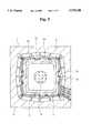
- FIG. 1is a plan view of a BGA package illustrating a first embodiment of the present invention.
- FIG. 2is a sectional view of the principal parts of the first embodiment of the present invention shown in FIG. 1.
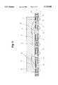
- FIG. 3is a plan view of a second embodiment of the semiconductor device of the present invention.
- FIG. 4is a plan view of a third embodiment of the semiconductor device of the present invention.
- FIG. 5is a sectional view of the principal parts of the third embodiment of the semiconductor device of the present invention shown in FIG. 4, viewed toward the line 5--5.
- FIG. 6is a plan view of a fourth embodiment of the semiconductor device of the present invention.
- FIG. 7is a sectional view of a conventional BGA.
- FIG. 8is a diagram showing the stress distribution at each part of the sectional view of FIG. 7.
- FIG. 9is a table showing the relationship between the material and the adherence strength.
- FIG. 1 and FIG. 2show the configuration of a first embodiment of the present invention.
- FIG. 1is a plan view of a BGA package.
- FIG. 2is a sectional view of the principal parts of the first embodiment of the present invention shown in FIG. 1.
- the same reference numeralsdesignate the same members referred to in the conventional technology.
- the semiconductor device of this first embodimentutilizes the conventional technology illustrated in FIG. 7 inasmuch as a thin copper foil is laminated on both sides of a resin substrate 1 and through-holes 2 are formed, after which a copper plated layer is provided by both non-electrolytic plating and electrolytic plating on all surfaces of the resin substrate 1 on both sides.
- a plating resist laminationis provided and developed by exposure to light to form a pattern mask, after which die patterns 3, 3a for the IC chip and a power supply pattern 3b and a lead pattern 4 are formed on the upper surface by pattern etching using an etching liquid, and pad electrodes 5 on which solder bumps are provided are formed on the lower surface.
- the outer shapes of the die patterns 3, 3aare greater than the outer shape of the IC chip 8.
- the die patterns 3, 3a (Vdd) on the upper surface of the resin substrate 1, a power supply pattern 3b (Vss), and a lead pattern 4are connected to the pad electrode 5 on the lower surface through the through holes 2.
- an insulating filmis formed on the corner sections corresponding to at least the corner A of the IC chip 8 and on other specified parts on the die patterns 3, 3a.
- a development-type liquid solder resist, a thermosetting solder resist (polyimide/epoxy), or an adhesive polyimide tape, or the likecan be used as the insulating film, but in this embodiment a development-type liquid solder resist film was formed using a solder resist process.
- corner resist films 6a, 6b, 6c, 6dcorresponding to the corners A of the IC chip 8 and a resist film 6 on the other specified parts are applied.
- the outer shapes of the corner resist films 6a, 6b, 6c, 6dare smaller than the outer shapes of the die patterns 3, 3a, so that the die bond patterns 3, 3aare exposed on the periphery of the corner resist films 6a, 6b, 6c, 6d.
- open sections of a plurality of same-shaped resist films 6 which have a surface on which it is possible to affix solderare formed in matrix form on the lower surface of the resin substrate 1.
- a circuit substrate 7is formed in this manner.
- Gold plating 31is provided on the die pattern section to which the resist films 6a, 6b, 6c, 6d are not affixed, and on the power supply pattern and the lead pattern of the circuit substrate 7.
- the IC chip 8is then mounted on the upper surface of the circuit substrate 7. At this time, the corner sections of the IC chip 8 are bonded to the corner section resist films 6a, 6b, 6c, 6d attached to the corners A of the die pattern 3 using a die bond 9. At the same time, the center area of the IC chip 8 is directly bonded to the die pattern 3 using the die bond 9.
- the power supply terminal of the IC chip 8the die pattern 3a, exposed at the outer periphery of the corner section resist films 6a, 6b, 6c, 6d, and the power supply pattern 3b which is formed outside the die pattern 3a, surrounding the die pattern 3a at certain intervals, are wire bonded using the bonding wire 10.
- the lead pattern 4 formed at the outer periphery of the circuit substrate 7 and the I/O terminal of the IC chip 8are wire bonded using the bonding wires 10.
- the IC chip 8is sealed in resin by a transfer mold using a thermosetting resin 11 to protect the IC chip 8 from light.
- Balls of solderare supplied to a plurality of pad electrodes 5 which are formed on the lower surface of the circuit substrate 7 and to which solder can adhere.
- the solder ballsare then heated in a heating furnace, whereby solder bumps 12 are formed. These solder bumps 12 allow the pad electrodes 5 to be conducted to a pattern of a mother board substrate (omitted from the drawing).
- a BGA 13is completed in this manner.
- the corner A of the IC chip 8is attached to the corner section resist films 6a, 6b, 6c, 6d using the die bond 9. Therefore, as shown in FIG. 9, the adhesive power is extremely high in comparison with the case of bonding on conventional gold plating via die bond.
- the external shape of the die patterns 3, 3ais greater than the external shape of the IC chip 8
- the corner section resist films 6a, 6b, 6c, and 6dare greater than the external shape of the IC chip 8 but smaller than the external shape of the die pattern 3a.
- the die pattern 3a and the power supply pattern 3b exposed on the outer periphery of the corner section resist films 6a, 6b, 6c, and 6d, and the power supply terminal of the IC chip 8are electrically connected by a plurality of bonding wires 10, it is possible to freely connect the power supply terminal to the die pattern 3a and the power supply pattern 3b without extending the die pattern 3a and the power supply pattern 3b to pull out these patterns corresponding to the position of the power supply terminal of the IC chip 8.
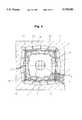
- FIG. 3is a plan view of a second embodiment of the semiconductor device of the present invention.
- a ring-shaped, integrally formed resist film 6eis provided in place of the corner section resist films 6a, 6b, 6c, and 6d which are independently formed in separate locations in the first embodiment.
- the semiconductor device of this configurationprovides the same actions and effects as the first embodiment of the semiconductor device of the present invention.
- FIG. 4 and FIG. 5show the configuration of a third embodiment of the present invention.
- FIG. 4is a plan view and
- FIG. 5is a sectional view of the principal parts of this third embodiment shown in FIG. 4, viewed at line 5--5.
- a die patterncomprises a main pattern 3, bonding patterns 3a and combination patterns 3d connecting the main pattern 3 and the bonding patterns 3a.
- the shape of the main pattern 3is smaller than the shape of the IC chip 8, and the bonding patterns 3a is formed at the outer periphery of the position where the IC chip 8 is mounted.
- the main pattern 3 and the bonding patterns 3aare electrically connected by the combination patterns 3d.
- the combination patterns 3dare formed in a radial configuration extending from the main pattern 3 and are not positioned at the corner section A of the IC chip 8 at which the thermal stress is concentrated.
- Power supply patterns 3bare provided around the periphery of the die patterns 3a surrounding these patterns with a certain interval.
- a resist filmis applied to a part almost at the center of the main pattern 3 and at positions corresponding to each corner section A of the IC chip 8 in almost the same manner as in the first embodiment.
- the corner section resist films 6a, 6b, 6c, and 6d formed at each corner sectionare independently attached at specific locations, and the resist film 6 is attached to the center area of the main pattern 3.
- the corner section resist films 6a, 6b, 6c, and 6dare independently attached at specific locations, and the resist film 6 is attached to the center area of the main pattern 3.
- the power supply terminal of the IC chip 8is electrically connected to the die patterns 3a and the power supply patterns 3b by the bonding wire 10.
- the corner section A of the IC chip 8 where thermal deformation mainly developsis attached by die bonding to the resist with a comparatively high adhesion strength.
- the combination patterns 3dare arranged so as not to position at the corner A, thereby alleviating generation of thermal deformation due to a difference in the thermal contraction ratio. As a result, peel of the corner section A of the IC chip 8 is reliably prevented, and the reliability of the semiconductor device is improved.
- the peripheral section of the IC chip 8 other than the corner section Ais directly attached to the circuit substrate 1 by the die bond material 9, the adhesion strength is high and reliability is considerably increased.
- the power supply terminal of the IC chip 8is electrically connected by the bonding wires 10
- the power supply terminalcan be freely connected to the die pattern 3a and the power supply pattern 3b without extending the die patterns 3a and the power supply patterns 3b by pulling out these corresponding to the position of the power supply terminal of the IC chip 8.
- FIG. 6is a plan view of a fourth embodiment of the semiconductor device of the present invention.
- corner section resist films 6a, 6b, 6c, and 6dare integrally formed as a ring-shaped resist film 6f.
- the semiconductor device of this configurationprovides the same actions and effects as the third embodiment of the semiconductor device of the present invention.
- the semiconductor device of the present invention with the above-mentioned configurationcan be built into various types of electrical apparatus.
Landscapes
- Engineering & Computer Science (AREA)
- Microelectronics & Electronic Packaging (AREA)
- Computer Hardware Design (AREA)
- Power Engineering (AREA)
- Physics & Mathematics (AREA)
- Condensed Matter Physics & Semiconductors (AREA)
- General Physics & Mathematics (AREA)
- Structures Or Materials For Encapsulating Or Coating Semiconductor Devices Or Solid State Devices (AREA)
- Wire Bonding (AREA)
- Die Bonding (AREA)
Abstract
Description
Claims (12)
Applications Claiming Priority (3)
| Application Number | Priority Date | Filing Date | Title |
|---|---|---|---|
| JP6-191502 | 1994-08-15 | ||
| JP19150294 | 1994-08-15 | ||
| PCT/JP1995/001622WO1996005613A1 (en) | 1994-08-15 | 1995-08-15 | Semiconductor device |
Publications (1)
| Publication Number | Publication Date |
|---|---|
| US5739588Atrue US5739588A (en) | 1998-04-14 |
Family
ID=16275723
Family Applications (1)
| Application Number | Title | Priority Date | Filing Date |
|---|---|---|---|
| US08/624,496Expired - LifetimeUS5739588A (en) | 1994-08-15 | 1995-08-15 | Semiconductor device |
Country Status (6)
| Country | Link |
|---|---|
| US (1) | US5739588A (en) |
| JP (1) | JP3578770B2 (en) |
| KR (1) | KR100201924B1 (en) |
| CN (1) | CN1063579C (en) |
| TW (1) | TW368745B (en) |
| WO (1) | WO1996005613A1 (en) |
Cited By (70)
| Publication number | Priority date | Publication date | Assignee | Title |
|---|---|---|---|---|
| US5864470A (en)* | 1996-12-30 | 1999-01-26 | Anam Semiconductor Inc. | Flexible circuit board for ball grid array semiconductor package |
| US5986339A (en)* | 1997-02-13 | 1999-11-16 | General Dynamics Information Systems, Inc. | Laminated multilayer substrates |
| US6107679A (en)* | 1997-12-22 | 2000-08-22 | Oki Electric Industry Co., Ltd. | Semiconductor device |
| US6157085A (en)* | 1998-04-07 | 2000-12-05 | Citizen Watch Co., Ltd. | Semiconductor device for preventing exfoliation from occurring between a semiconductor chip and a resin substrate |
| US6476486B1 (en)* | 1997-10-30 | 2002-11-05 | Agilent Technologies, Inc. | Ball grid array package with supplemental electronic component |
| US6479760B2 (en)* | 1999-02-15 | 2002-11-12 | Mitsubishi Gas Chemical Company, Inc. | Printed wiring board for semiconductor plastic package |
| US6489682B1 (en)* | 2000-01-20 | 2002-12-03 | Advanced Semiconductor Engineering, Inc. | Ball grid array semiconductor package and substrate therefor |
| US20030015785A1 (en)* | 1995-11-29 | 2003-01-23 | Hitachi, Ltd. | BGA type semiconductor device and electronic equipment using the same |
| US6537842B2 (en) | 2000-06-08 | 2003-03-25 | Micron Technology, Inc. | Methods for fabricating protective structures for bond wires |
| US6590275B2 (en)* | 1997-07-30 | 2003-07-08 | Hitachi, Ltd. | Ball grid array type semiconductor package having a flexible substrate |
| US6657294B2 (en)* | 2000-05-23 | 2003-12-02 | Koninklijke Philips Electronics N.V. | Data carrier having an IC module with a protection mechanism for protecting the parts of the IC module from mechanical stress |
| US20040007386A1 (en)* | 2002-07-11 | 2004-01-15 | S & S Technology Corporation | Structure of printed circuit board (PCB) |
| US6825569B2 (en)* | 1998-11-12 | 2004-11-30 | Micron Technology, Inc. | BGA package having substrate with patterned solder mask defining open die attach area |
| US20050041398A1 (en)* | 2002-05-01 | 2005-02-24 | Huemoeller Ronald Patrick | Integrated circuit substrate having embedded back-side access conductors and vias |
| US20050136558A1 (en)* | 2003-12-18 | 2005-06-23 | Wang James J. | Stacked semiconductor device assembly and method for forming |
| US20050167850A1 (en)* | 1995-12-19 | 2005-08-04 | Moden Walter L. | Flip-chip adaptor package for bare die |
| US6930042B1 (en)* | 1999-05-11 | 2005-08-16 | Infineon Technologies Ag | Method for producing a semiconductor component with at least one encapsulated chip on a substrate |
| US6930256B1 (en)* | 2002-05-01 | 2005-08-16 | Amkor Technology, Inc. | Integrated circuit substrate having laser-embedded conductive patterns and method therefor |
| US20050285266A1 (en)* | 2004-06-18 | 2005-12-29 | Martin Reiss | Arrangement for increasing the reliability of substrate-based BGA packages |
| US20060097369A1 (en)* | 1996-12-04 | 2006-05-11 | Seiko Epson Corporation | Electronic component and semiconductor device, method of making the same and method of mounting the same, circuit board, and electronic instrument |
| US20060145322A1 (en)* | 2004-12-27 | 2006-07-06 | Kouji Takahashi | Circuit device and portable device |
| US20060249843A1 (en)* | 1996-12-04 | 2006-11-09 | Seiko Epson Corporation | Semiconductor device, circuit board, and electronic instrument |
| US7145238B1 (en) | 2004-05-05 | 2006-12-05 | Amkor Technology, Inc. | Semiconductor package and substrate having multi-level vias |
| US20070096307A1 (en)* | 2005-10-14 | 2007-05-03 | Nec Electronics Corporation | Semiconductor device |
| US20080043447A1 (en)* | 2002-05-01 | 2008-02-21 | Amkor Technology, Inc. | Semiconductor package having laser-embedded terminals |
| US7334326B1 (en) | 2001-06-19 | 2008-02-26 | Amkor Technology, Inc. | Method for making an integrated circuit substrate having embedded passive components |
| US7501338B1 (en) | 2001-06-19 | 2009-03-10 | Amkor Technology, Inc. | Semiconductor package substrate fabrication method |
| US7548430B1 (en) | 2002-05-01 | 2009-06-16 | Amkor Technology, Inc. | Buildup dielectric and metallization process and semiconductor package |
| US7550857B1 (en) | 2006-11-16 | 2009-06-23 | Amkor Technology, Inc. | Stacked redistribution layer (RDL) die assembly package |
| US7589398B1 (en) | 2006-10-04 | 2009-09-15 | Amkor Technology, Inc. | Embedded metal features structure |
| US7633765B1 (en) | 2004-03-23 | 2009-12-15 | Amkor Technology, Inc. | Semiconductor package including a top-surface metal layer for implementing circuit features |
| US7670962B2 (en) | 2002-05-01 | 2010-03-02 | Amkor Technology, Inc. | Substrate having stiffener fabrication method |
| US7750250B1 (en) | 2006-12-22 | 2010-07-06 | Amkor Technology, Inc. | Blind via capture pad structure |
| US7752752B1 (en) | 2007-01-09 | 2010-07-13 | Amkor Technology, Inc. | Method of fabricating an embedded circuit pattern |
| US7960827B1 (en) | 2009-04-09 | 2011-06-14 | Amkor Technology, Inc. | Thermal via heat spreader package and method |
| USRE43112E1 (en) | 1998-05-04 | 2012-01-17 | Round Rock Research, Llc | Stackable ball grid array package |
| US8222538B1 (en) | 2009-06-12 | 2012-07-17 | Amkor Technology, Inc. | Stackable via package and method |
| US8294276B1 (en) | 2010-05-27 | 2012-10-23 | Amkor Technology, Inc. | Semiconductor device and fabricating method thereof |
| US8300423B1 (en) | 2010-05-25 | 2012-10-30 | Amkor Technology, Inc. | Stackable treated via package and method |
| US8323771B1 (en) | 2007-08-15 | 2012-12-04 | Amkor Technology, Inc. | Straight conductor blind via capture pad structure and fabrication method |
| US8338229B1 (en) | 2010-07-30 | 2012-12-25 | Amkor Technology, Inc. | Stackable plasma cleaned via package and method |
| US8337657B1 (en) | 2010-10-27 | 2012-12-25 | Amkor Technology, Inc. | Mechanical tape separation package and method |
| US8471154B1 (en) | 2009-08-06 | 2013-06-25 | Amkor Technology, Inc. | Stackable variable height via package and method |
| US8482134B1 (en) | 2010-11-01 | 2013-07-09 | Amkor Technology, Inc. | Stackable package and method |
| US8525318B1 (en) | 2010-11-10 | 2013-09-03 | Amkor Technology, Inc. | Semiconductor device and fabricating method thereof |
| US8535961B1 (en) | 2010-12-09 | 2013-09-17 | Amkor Technology, Inc. | Light emitting diode (LED) package and method |
| US8536462B1 (en) | 2010-01-22 | 2013-09-17 | Amkor Technology, Inc. | Flex circuit package and method |
| US8557629B1 (en) | 2010-12-03 | 2013-10-15 | Amkor Technology, Inc. | Semiconductor device having overlapped via apertures |
| US8623753B1 (en) | 2009-05-28 | 2014-01-07 | Amkor Technology, Inc. | Stackable protruding via package and method |
| US8633598B1 (en) | 2011-09-20 | 2014-01-21 | Amkor Technology, Inc. | Underfill contacting stacking balls package fabrication method and structure |
| US8653674B1 (en) | 2011-09-15 | 2014-02-18 | Amkor Technology, Inc. | Electronic component package fabrication method and structure |
| US8717775B1 (en) | 2010-08-02 | 2014-05-06 | Amkor Technology, Inc. | Fingerprint sensor package and method |
| US8796561B1 (en) | 2009-10-05 | 2014-08-05 | Amkor Technology, Inc. | Fan out build up substrate stackable package and method |
| US8826531B1 (en) | 2005-04-05 | 2014-09-09 | Amkor Technology, Inc. | Method for making an integrated circuit substrate having laminated laser-embedded circuit layers |
| US8872329B1 (en) | 2009-01-09 | 2014-10-28 | Amkor Technology, Inc. | Extended landing pad substrate package structure and method |
| US8890329B2 (en) | 2011-04-26 | 2014-11-18 | Amkor Technology, Inc. | Semiconductor device |
| US8937381B1 (en) | 2009-12-03 | 2015-01-20 | Amkor Technology, Inc. | Thin stackable package and method |
| US9013011B1 (en) | 2011-03-11 | 2015-04-21 | Amkor Technology, Inc. | Stacked and staggered die MEMS package and method |
| US9029962B1 (en) | 2011-10-12 | 2015-05-12 | Amkor Technology, Inc. | Molded cavity substrate MEMS package fabrication method and structure |
| US9391043B2 (en) | 2012-11-20 | 2016-07-12 | Amkor Technology, Inc. | Semiconductor device and manufacturing method thereof |
| US9543242B1 (en) | 2013-01-29 | 2017-01-10 | Amkor Technology, Inc. | Semiconductor package and fabricating method thereof |
| US9691635B1 (en) | 2002-05-01 | 2017-06-27 | Amkor Technology, Inc. | Buildup dielectric layer having metallization pattern semiconductor package fabrication method |
| US9691734B1 (en) | 2009-12-07 | 2017-06-27 | Amkor Technology, Inc. | Method of forming a plurality of electronic component packages |
| US9704842B2 (en) | 2013-11-04 | 2017-07-11 | Amkor Technology, Inc. | Interposer, manufacturing method thereof, semiconductor package using the same, and method for fabricating the semiconductor package |
| US9704747B2 (en) | 2013-03-29 | 2017-07-11 | Amkor Technology, Inc. | Semiconductor device and manufacturing method thereof |
| US9721872B1 (en) | 2011-02-18 | 2017-08-01 | Amkor Technology, Inc. | Methods and structures for increasing the allowable die size in TMV packages |
| US9748154B1 (en) | 2010-11-04 | 2017-08-29 | Amkor Technology, Inc. | Wafer level fan out semiconductor device and manufacturing method thereof |
| US9960328B2 (en) | 2016-09-06 | 2018-05-01 | Amkor Technology, Inc. | Semiconductor device and manufacturing method thereof |
| US10811277B2 (en) | 2004-03-23 | 2020-10-20 | Amkor Technology, Inc. | Encapsulated semiconductor package |
| US11081370B2 (en) | 2004-03-23 | 2021-08-03 | Amkor Technology Singapore Holding Pte. Ltd. | Methods of manufacturing an encapsulated semiconductor device |
Families Citing this family (8)
| Publication number | Priority date | Publication date | Assignee | Title |
|---|---|---|---|---|
| JP3959697B2 (en)* | 1997-01-30 | 2007-08-15 | ソニー株式会社 | Semiconductor device, semiconductor device manufacturing method, and wiring board |
| JPH10214917A (en)* | 1997-01-30 | 1998-08-11 | Sony Corp | Semiconductor device, its manufacture, and wiring board |
| JP4701563B2 (en)* | 2001-08-23 | 2011-06-15 | 日本テキサス・インスツルメンツ株式会社 | Semiconductor chip mounting substrate and semiconductor device using the same |
| CN102496585A (en)* | 2011-12-19 | 2012-06-13 | 南通富士通微电子股份有限公司 | Novel wafer level packaging method |
| CN102437065A (en)* | 2011-12-19 | 2012-05-02 | 南通富士通微电子股份有限公司 | High-reliability chip scale packaging method |
| CN102931098B (en)* | 2012-11-08 | 2015-06-03 | 南通富士通微电子股份有限公司 | Chip packaging method |
| US9589815B2 (en) | 2012-11-08 | 2017-03-07 | Nantong Fujitsu Microelectronics Co., Ltd. | Semiconductor IC packaging methods and structures |
| JP6252412B2 (en)* | 2014-09-10 | 2017-12-27 | 三菱電機株式会社 | Semiconductor device |
Citations (4)
| Publication number | Priority date | Publication date | Assignee | Title |
|---|---|---|---|---|
| JPS61218139A (en)* | 1985-03-25 | 1986-09-27 | Hitachi Chiyou Lsi Eng Kk | Semiconductor device |
| JPH05291487A (en)* | 1992-03-28 | 1993-11-05 | Samsung Electron Co Ltd | Semiconductor lead frame |
| US5285352A (en)* | 1992-07-15 | 1994-02-08 | Motorola, Inc. | Pad array semiconductor device with thermal conductor and process for making the same |
| US5397917A (en)* | 1993-04-26 | 1995-03-14 | Motorola, Inc. | Semiconductor package capable of spreading heat |
- 1995
- 1995-08-09TWTW084108278Apatent/TW368745B/enactive
- 1995-08-15JPJP50719796Apatent/JP3578770B2/ennot_activeExpired - Fee Related
- 1995-08-15USUS08/624,496patent/US5739588A/ennot_activeExpired - Lifetime
- 1995-08-15WOPCT/JP1995/001622patent/WO1996005613A1/enactiveApplication Filing
- 1995-08-15CNCN95190765Apatent/CN1063579C/ennot_activeExpired - Fee Related
- 1995-08-15KRKR1019960701568Apatent/KR100201924B1/ennot_activeExpired - Fee Related
Patent Citations (4)
| Publication number | Priority date | Publication date | Assignee | Title |
|---|---|---|---|---|
| JPS61218139A (en)* | 1985-03-25 | 1986-09-27 | Hitachi Chiyou Lsi Eng Kk | Semiconductor device |
| JPH05291487A (en)* | 1992-03-28 | 1993-11-05 | Samsung Electron Co Ltd | Semiconductor lead frame |
| US5285352A (en)* | 1992-07-15 | 1994-02-08 | Motorola, Inc. | Pad array semiconductor device with thermal conductor and process for making the same |
| US5397917A (en)* | 1993-04-26 | 1995-03-14 | Motorola, Inc. | Semiconductor package capable of spreading heat |
Cited By (163)
| Publication number | Priority date | Publication date | Assignee | Title |
|---|---|---|---|---|
| US20030015785A1 (en)* | 1995-11-29 | 2003-01-23 | Hitachi, Ltd. | BGA type semiconductor device and electronic equipment using the same |
| US7164194B2 (en) | 1995-11-29 | 2007-01-16 | Renesas Technology Corp. | BGA type semiconductor device and electronic equipment using the same |
| US7291909B2 (en)* | 1995-11-29 | 2007-11-06 | Renesas Technology Corp. | BGA type semiconductor device and electronic equipment using the same |
| US20030015786A1 (en)* | 1995-11-29 | 2003-01-23 | Hitachi, Ltd. | BGA type semiconductor device and electronic equipment using the same |
| US7329945B2 (en) | 1995-12-19 | 2008-02-12 | Micron Technology, Inc. | Flip-chip adaptor package for bare die |
| US7381591B2 (en) | 1995-12-19 | 2008-06-03 | Micron Technology, Inc. | Flip-chip adaptor package for bare die |
| US8164175B2 (en) | 1995-12-19 | 2012-04-24 | Round Rock Research, Llc | Stackable semiconductor device assemblies |
| US20050167850A1 (en)* | 1995-12-19 | 2005-08-04 | Moden Walter L. | Flip-chip adaptor package for bare die |
| US8198138B2 (en) | 1995-12-19 | 2012-06-12 | Round Rock Research, Llc | Methods for providing and using grid array packages |
| US8299598B2 (en) | 1995-12-19 | 2012-10-30 | Round Rock Research, Llc | Grid array packages and assemblies including the same |
| US8049317B2 (en) | 1995-12-19 | 2011-11-01 | Round Rock Research, Llc | Grid array packages |
| US7842598B2 (en) | 1996-12-04 | 2010-11-30 | Seiko Epson Corporation | Electronic component and semiconductor device, method of making the same and method of mounting the same, circuit board, and electronic instrument |
| US20100273311A1 (en)* | 1996-12-04 | 2010-10-28 | Seiko Epson Corporation | Electronic component and semiconductor device, method of making the same and method of mounting the same, circuit board, and electronic instrument |
| US20090174068A1 (en)* | 1996-12-04 | 2009-07-09 | Seiko Epson Corporation | Semiconductor device, circuit board, and electronic instrument |
| US20090181521A1 (en)* | 1996-12-04 | 2009-07-16 | Seiko Epson Corporation | Electronic component and semiconductor device, method of making the same and method of mounting the same, circuit board, and electronic instrument |
| US8384213B2 (en) | 1996-12-04 | 2013-02-26 | Seiko Epson Corporation | Semiconductor device, circuit board, and electronic instrument |
| US8115284B2 (en) | 1996-12-04 | 2012-02-14 | Seiko Epson Corporation | Electronic component and semiconductor device, method of making the same and method of mounting the same, circuit board and electronic instrument |
| US20060131705A1 (en)* | 1996-12-04 | 2006-06-22 | Seiko Epson Corporation | Electronic component and semiconductor device, method of making the same and method of mounting the same, circuit board, and electronic instrument |
| US7470979B2 (en) | 1996-12-04 | 2008-12-30 | Seiko Epson Corporation | Electronic component and semiconductor device, method of making the same and method of mounting the same, circuit board, and electronic instrument |
| US20060097369A1 (en)* | 1996-12-04 | 2006-05-11 | Seiko Epson Corporation | Electronic component and semiconductor device, method of making the same and method of mounting the same, circuit board, and electronic instrument |
| US7511362B2 (en) | 1996-12-04 | 2009-03-31 | Seiko Epson Corporation | Electronic component and semiconductor device, method of making the same and method of mounting the same, circuit board, and electronic instrument |
| US20060249843A1 (en)* | 1996-12-04 | 2006-11-09 | Seiko Epson Corporation | Semiconductor device, circuit board, and electronic instrument |
| US7521796B2 (en) | 1996-12-04 | 2009-04-21 | Seiko Epson Corporation | Method of making the semiconductor device, circuit board, and electronic instrument |
| US7888260B2 (en) | 1996-12-04 | 2011-02-15 | Seiko Epson Corporation | Method of making electronic device |
| US20110095432A1 (en)* | 1996-12-04 | 2011-04-28 | Seiko Epson Corporation | Electronic component and semiconductor device, method of making the same and method of mounting the same, circuit board and electronic instrument |
| US5864470A (en)* | 1996-12-30 | 1999-01-26 | Anam Semiconductor Inc. | Flexible circuit board for ball grid array semiconductor package |
| US5986339A (en)* | 1997-02-13 | 1999-11-16 | General Dynamics Information Systems, Inc. | Laminated multilayer substrates |
| US6590275B2 (en)* | 1997-07-30 | 2003-07-08 | Hitachi, Ltd. | Ball grid array type semiconductor package having a flexible substrate |
| US6476486B1 (en)* | 1997-10-30 | 2002-11-05 | Agilent Technologies, Inc. | Ball grid array package with supplemental electronic component |
| US6107679A (en)* | 1997-12-22 | 2000-08-22 | Oki Electric Industry Co., Ltd. | Semiconductor device |
| US6157085A (en)* | 1998-04-07 | 2000-12-05 | Citizen Watch Co., Ltd. | Semiconductor device for preventing exfoliation from occurring between a semiconductor chip and a resin substrate |
| USRE43112E1 (en) | 1998-05-04 | 2012-01-17 | Round Rock Research, Llc | Stackable ball grid array package |
| US6825569B2 (en)* | 1998-11-12 | 2004-11-30 | Micron Technology, Inc. | BGA package having substrate with patterned solder mask defining open die attach area |
| US6479760B2 (en)* | 1999-02-15 | 2002-11-12 | Mitsubishi Gas Chemical Company, Inc. | Printed wiring board for semiconductor plastic package |
| US6930042B1 (en)* | 1999-05-11 | 2005-08-16 | Infineon Technologies Ag | Method for producing a semiconductor component with at least one encapsulated chip on a substrate |
| US6489682B1 (en)* | 2000-01-20 | 2002-12-03 | Advanced Semiconductor Engineering, Inc. | Ball grid array semiconductor package and substrate therefor |
| US6657294B2 (en)* | 2000-05-23 | 2003-12-02 | Koninklijke Philips Electronics N.V. | Data carrier having an IC module with a protection mechanism for protecting the parts of the IC module from mechanical stress |
| US7087984B2 (en)* | 2000-06-08 | 2006-08-08 | Micron Technology, Inc. | Methods for protecting intermediate conductive elements of semiconductor device assemblies |
| US20050014323A1 (en)* | 2000-06-08 | 2005-01-20 | Salman Akram | Methods for protecting intermediate conductive elements of semiconductor device assemblies |
| US6537842B2 (en) | 2000-06-08 | 2003-03-25 | Micron Technology, Inc. | Methods for fabricating protective structures for bond wires |
| US20050173790A1 (en)* | 2000-06-08 | 2005-08-11 | Salman Akram | Protective structures for bond wires |
| US6913988B2 (en) | 2000-06-08 | 2005-07-05 | Micron Technology, Inc. | Methods for fabricating semiconductor device test apparatus that include protective structures for intermediate conductive elements |
| US6890787B2 (en) | 2000-06-08 | 2005-05-10 | Micron Technology, Inc. | Methods for protecting intermediate conductive elements of semiconductor device assemblies |
| US20050042856A1 (en)* | 2000-06-08 | 2005-02-24 | Salman Akram | Programmed material consolidation processes for protecting intermediate conductive structures |
| US6946378B2 (en) | 2000-06-08 | 2005-09-20 | Micron Technology, Inc. | Methods for fabricating protective structures for bond wires |
| US20040032020A1 (en)* | 2000-06-08 | 2004-02-19 | Salman Akram | Protective structures for bond wires |
| US6963127B2 (en) | 2000-06-08 | 2005-11-08 | Micron Technology, Inc. | Protective structures for bond wires |
| US7084012B2 (en)* | 2000-06-08 | 2006-08-01 | Micron Technology, Inc. | Programmed material consolidation processes for protecting intermediate conductive structures |
| US20030186496A1 (en)* | 2000-06-08 | 2003-10-02 | Salman Akram | Methods for protecting intermediate conductive elements of semiconductor device assemblies |
| US20030180974A1 (en)* | 2000-06-08 | 2003-09-25 | Salman Akram | Methods for fabricating semiconductor device test apparatus that include protective structures for intermediate conductive elements |
| US6611053B2 (en)* | 2000-06-08 | 2003-08-26 | Micron Technology, Inc. | Protective structure for bond wires |
| US7501338B1 (en) | 2001-06-19 | 2009-03-10 | Amkor Technology, Inc. | Semiconductor package substrate fabrication method |
| US7334326B1 (en) | 2001-06-19 | 2008-02-26 | Amkor Technology, Inc. | Method for making an integrated circuit substrate having embedded passive components |
| US7185426B1 (en) | 2002-05-01 | 2007-03-06 | Amkor Technology, Inc. | Method of manufacturing a semiconductor package |
| US7670962B2 (en) | 2002-05-01 | 2010-03-02 | Amkor Technology, Inc. | Substrate having stiffener fabrication method |
| US7399661B2 (en) | 2002-05-01 | 2008-07-15 | Amkor Technology, Inc. | Method for making an integrated circuit substrate having embedded back-side access conductors and vias |
| US7548430B1 (en) | 2002-05-01 | 2009-06-16 | Amkor Technology, Inc. | Buildup dielectric and metallization process and semiconductor package |
| US9691635B1 (en) | 2002-05-01 | 2017-06-27 | Amkor Technology, Inc. | Buildup dielectric layer having metallization pattern semiconductor package fabrication method |
| US20050041398A1 (en)* | 2002-05-01 | 2005-02-24 | Huemoeller Ronald Patrick | Integrated circuit substrate having embedded back-side access conductors and vias |
| US20080043447A1 (en)* | 2002-05-01 | 2008-02-21 | Amkor Technology, Inc. | Semiconductor package having laser-embedded terminals |
| US8322030B1 (en)* | 2002-05-01 | 2012-12-04 | Amkor Technology, Inc. | Circuit-on-foil process for manufacturing a laminated semiconductor package substrate having embedded conductive patterns |
| US8341835B1 (en) | 2002-05-01 | 2013-01-01 | Amkor Technology, Inc. | Buildup dielectric layer having metallization pattern semiconductor package fabrication method |
| US6930256B1 (en)* | 2002-05-01 | 2005-08-16 | Amkor Technology, Inc. | Integrated circuit substrate having laser-embedded conductive patterns and method therefor |
| US7671457B1 (en) | 2002-05-01 | 2010-03-02 | Amkor Technology, Inc. | Semiconductor package including top-surface terminals for mounting another semiconductor package |
| US8026587B1 (en) | 2002-05-01 | 2011-09-27 | Amkor Technology, Inc. | Semiconductor package including top-surface terminals for mounting another semiconductor package |
| US9812386B1 (en) | 2002-05-01 | 2017-11-07 | Amkor Technology, Inc. | Encapsulated semiconductor package |
| US7312103B1 (en) | 2002-05-01 | 2007-12-25 | Amkor Technology, Inc. | Method for making an integrated circuit substrate having laser-embedded conductive patterns |
| US10461006B1 (en) | 2002-05-01 | 2019-10-29 | Amkor Technology, Inc. | Encapsulated semiconductor package |
| US7297562B1 (en) | 2002-05-01 | 2007-11-20 | Amkor Technology, Inc. | Circuit-on-foil process for manufacturing a laminated semiconductor package substrate having embedded conductive patterns |
| US8110909B1 (en) | 2002-05-01 | 2012-02-07 | Amkor Technology, Inc. | Semiconductor package including top-surface terminals for mounting another semiconductor package |
| US8316536B1 (en) | 2002-05-01 | 2012-11-27 | Amkor Technology, Inc. | Multi-level circuit substrate fabrication method |
| US20040007386A1 (en)* | 2002-07-11 | 2004-01-15 | S & S Technology Corporation | Structure of printed circuit board (PCB) |
| US20050136558A1 (en)* | 2003-12-18 | 2005-06-23 | Wang James J. | Stacked semiconductor device assembly and method for forming |
| US7132303B2 (en) | 2003-12-18 | 2006-11-07 | Freescale Semiconductor, Inc. | Stacked semiconductor device assembly and method for forming |
| US10811277B2 (en) | 2004-03-23 | 2020-10-20 | Amkor Technology, Inc. | Encapsulated semiconductor package |
| US8018068B1 (en) | 2004-03-23 | 2011-09-13 | Amkor Technology, Inc. | Semiconductor package including a top-surface metal layer for implementing circuit features |
| US11081370B2 (en) | 2004-03-23 | 2021-08-03 | Amkor Technology Singapore Holding Pte. Ltd. | Methods of manufacturing an encapsulated semiconductor device |
| US7633765B1 (en) | 2004-03-23 | 2009-12-15 | Amkor Technology, Inc. | Semiconductor package including a top-surface metal layer for implementing circuit features |
| US8227338B1 (en) | 2004-03-23 | 2012-07-24 | Amkor Technology, Inc. | Semiconductor package including a top-surface metal layer for implementing circuit features |
| US11094560B1 (en) | 2004-03-23 | 2021-08-17 | Amkor Technology Singapore Holding Pte. Ltd. | Encapsulated semiconductor package |
| US7145238B1 (en) | 2004-05-05 | 2006-12-05 | Amkor Technology, Inc. | Semiconductor package and substrate having multi-level vias |
| US7365006B1 (en) | 2004-05-05 | 2008-04-29 | Amkor Technology, Inc. | Semiconductor package and substrate having multi-level vias fabrication method |
| US20050285266A1 (en)* | 2004-06-18 | 2005-12-29 | Martin Reiss | Arrangement for increasing the reliability of substrate-based BGA packages |
| US20060145322A1 (en)* | 2004-12-27 | 2006-07-06 | Kouji Takahashi | Circuit device and portable device |
| US7417309B2 (en) | 2004-12-27 | 2008-08-26 | Sanyo Electric Co., Ltd. | Circuit device and portable device with symmetrical arrangement |
| US8826531B1 (en) | 2005-04-05 | 2014-09-09 | Amkor Technology, Inc. | Method for making an integrated circuit substrate having laminated laser-embedded circuit layers |
| US20070096307A1 (en)* | 2005-10-14 | 2007-05-03 | Nec Electronics Corporation | Semiconductor device |
| US11848214B2 (en) | 2006-08-01 | 2023-12-19 | Amkor Technology Singapore Holding Pte. Ltd. | Encapsulated semiconductor package |
| US7911037B1 (en) | 2006-10-04 | 2011-03-22 | Amkor Technology, Inc. | Method and structure for creating embedded metal features |
| US7589398B1 (en) | 2006-10-04 | 2009-09-15 | Amkor Technology, Inc. | Embedded metal features structure |
| US8629546B1 (en) | 2006-11-16 | 2014-01-14 | Amkor Technology, Inc. | Stacked redistribution layer (RDL) die assembly package |
| US7550857B1 (en) | 2006-11-16 | 2009-06-23 | Amkor Technology, Inc. | Stacked redistribution layer (RDL) die assembly package |
| US7825520B1 (en) | 2006-11-16 | 2010-11-02 | Amkor Technology, Inc. | Stacked redistribution layer (RDL) die assembly package |
| US8203203B1 (en) | 2006-11-16 | 2012-06-19 | Amkor Technology, Inc. | Stacked redistribution layer (RDL) die assembly package |
| US7750250B1 (en) | 2006-12-22 | 2010-07-06 | Amkor Technology, Inc. | Blind via capture pad structure |
| US8671565B1 (en) | 2006-12-22 | 2014-03-18 | Amkor Technology, Inc. | Blind via capture pad structure fabrication method |
| US7752752B1 (en) | 2007-01-09 | 2010-07-13 | Amkor Technology, Inc. | Method of fabricating an embedded circuit pattern |
| US8323771B1 (en) | 2007-08-15 | 2012-12-04 | Amkor Technology, Inc. | Straight conductor blind via capture pad structure and fabrication method |
| US8872329B1 (en) | 2009-01-09 | 2014-10-28 | Amkor Technology, Inc. | Extended landing pad substrate package structure and method |
| US9462704B1 (en) | 2009-01-09 | 2016-10-04 | Amkor Technology, Inc. | Extended landing pad substrate package structure and method |
| US7960827B1 (en) | 2009-04-09 | 2011-06-14 | Amkor Technology, Inc. | Thermal via heat spreader package and method |
| US8623753B1 (en) | 2009-05-28 | 2014-01-07 | Amkor Technology, Inc. | Stackable protruding via package and method |
| US10034372B1 (en) | 2009-06-12 | 2018-07-24 | Amkor Technology, Inc. | Stackable via package and method |
| US10206285B1 (en) | 2009-06-12 | 2019-02-12 | Amkor Technology, Inc. | Stackable via package and method |
| US8704368B1 (en) | 2009-06-12 | 2014-04-22 | Amkor Technology, Inc. | Stackable via package and method |
| US10548221B1 (en) | 2009-06-12 | 2020-01-28 | Amkor Technology, Inc. | Stackable via package and method |
| US11089685B2 (en) | 2009-06-12 | 2021-08-10 | Amkor Technology Singapore Holding Pte. Ltd. | Stackable via package and method |
| US8222538B1 (en) | 2009-06-12 | 2012-07-17 | Amkor Technology, Inc. | Stackable via package and method |
| US12035472B2 (en) | 2009-06-12 | 2024-07-09 | Amkor Technology Singapore Holding Ptd. Ltd. | Stackable via package and method |
| US9730327B1 (en) | 2009-06-12 | 2017-08-08 | Amkor Technology, Inc. | Stackable via package and method |
| US11700692B2 (en) | 2009-06-12 | 2023-07-11 | Amkor Technology Singapore Holding Pte. Ltd. | Stackable via package and method |
| US9012789B1 (en) | 2009-06-12 | 2015-04-21 | Amkor Technology, Inc. | Stackable via package and method |
| US10257942B1 (en) | 2009-08-06 | 2019-04-09 | Amkor Technology, Inc. | Stackable variable height via package and method |
| US8471154B1 (en) | 2009-08-06 | 2013-06-25 | Amkor Technology, Inc. | Stackable variable height via package and method |
| US8796561B1 (en) | 2009-10-05 | 2014-08-05 | Amkor Technology, Inc. | Fan out build up substrate stackable package and method |
| US8937381B1 (en) | 2009-12-03 | 2015-01-20 | Amkor Technology, Inc. | Thin stackable package and method |
| US10546833B2 (en) | 2009-12-07 | 2020-01-28 | Amkor Technology, Inc. | Method of forming a plurality of electronic component packages |
| US9691734B1 (en) | 2009-12-07 | 2017-06-27 | Amkor Technology, Inc. | Method of forming a plurality of electronic component packages |
| US8536462B1 (en) | 2010-01-22 | 2013-09-17 | Amkor Technology, Inc. | Flex circuit package and method |
| US8300423B1 (en) | 2010-05-25 | 2012-10-30 | Amkor Technology, Inc. | Stackable treated via package and method |
| US8294276B1 (en) | 2010-05-27 | 2012-10-23 | Amkor Technology, Inc. | Semiconductor device and fabricating method thereof |
| US8338229B1 (en) | 2010-07-30 | 2012-12-25 | Amkor Technology, Inc. | Stackable plasma cleaned via package and method |
| US8717775B1 (en) | 2010-08-02 | 2014-05-06 | Amkor Technology, Inc. | Fingerprint sensor package and method |
| US8337657B1 (en) | 2010-10-27 | 2012-12-25 | Amkor Technology, Inc. | Mechanical tape separation package and method |
| US8753730B1 (en) | 2010-10-27 | 2014-06-17 | Amkor Technology, Inc. | Mechanical tape separation package |
| US9496210B1 (en) | 2010-11-01 | 2016-11-15 | Amkor Technology, Inc. | Stackable package and method |
| US8482134B1 (en) | 2010-11-01 | 2013-07-09 | Amkor Technology, Inc. | Stackable package and method |
| US12009343B1 (en) | 2010-11-01 | 2024-06-11 | Amkor Technology Singapore Holding Pte. Ltd. | Stackable package and method |
| US10903181B2 (en) | 2010-11-04 | 2021-01-26 | Amkor Technology Singapore Holding Pte. Ltd. | Wafer level fan out semiconductor device and manufacturing method thereof |
| US9748154B1 (en) | 2010-11-04 | 2017-08-29 | Amkor Technology, Inc. | Wafer level fan out semiconductor device and manufacturing method thereof |
| US11855023B2 (en) | 2010-11-04 | 2023-12-26 | Amkor Technology Singapore Holding Pte. Ltd. | Wafer level fan out semiconductor device and manufacturing method thereof |
| US8525318B1 (en) | 2010-11-10 | 2013-09-03 | Amkor Technology, Inc. | Semiconductor device and fabricating method thereof |
| US8557629B1 (en) | 2010-12-03 | 2013-10-15 | Amkor Technology, Inc. | Semiconductor device having overlapped via apertures |
| US9837331B1 (en) | 2010-12-03 | 2017-12-05 | Amkor Technology, Inc. | Semiconductor device having overlapped via apertures |
| US9177932B1 (en) | 2010-12-03 | 2015-11-03 | Amkor Technology, Inc. | Semiconductor device having overlapped via apertures |
| US8535961B1 (en) | 2010-12-09 | 2013-09-17 | Amkor Technology, Inc. | Light emitting diode (LED) package and method |
| US9721872B1 (en) | 2011-02-18 | 2017-08-01 | Amkor Technology, Inc. | Methods and structures for increasing the allowable die size in TMV packages |
| US11488892B2 (en) | 2011-02-18 | 2022-11-01 | Amkor Technology Singapore Holding Pte. Ltd. | Methods and structures for increasing the allowable die size in TMV packages |
| US10347562B1 (en) | 2011-02-18 | 2019-07-09 | Amkor Technology, Inc. | Methods and structures for increasing the allowable die size in TMV packages |
| US9013011B1 (en) | 2011-03-11 | 2015-04-21 | Amkor Technology, Inc. | Stacked and staggered die MEMS package and method |
| US8890329B2 (en) | 2011-04-26 | 2014-11-18 | Amkor Technology, Inc. | Semiconductor device |
| US8653674B1 (en) | 2011-09-15 | 2014-02-18 | Amkor Technology, Inc. | Electronic component package fabrication method and structure |
| US8941250B1 (en) | 2011-09-15 | 2015-01-27 | Amkor Technology, Inc. | Electronic component package fabrication method and structure |
| US8890337B1 (en) | 2011-09-20 | 2014-11-18 | Amkor Technology, Inc. | Column and stacking balls package fabrication method and structure |
| US8633598B1 (en) | 2011-09-20 | 2014-01-21 | Amkor Technology, Inc. | Underfill contacting stacking balls package fabrication method and structure |
| US9029962B1 (en) | 2011-10-12 | 2015-05-12 | Amkor Technology, Inc. | Molded cavity substrate MEMS package fabrication method and structure |
| US9391043B2 (en) | 2012-11-20 | 2016-07-12 | Amkor Technology, Inc. | Semiconductor device and manufacturing method thereof |
| US10679952B2 (en) | 2012-11-20 | 2020-06-09 | Amkor Technology, Inc. | Semiconductor device having an encapsulated front side and interposer and manufacturing method thereof |
| US9728514B2 (en) | 2012-11-20 | 2017-08-08 | Amkor Technology, Inc. | Semiconductor device and manufacturing method thereof |
| US11527496B2 (en) | 2012-11-20 | 2022-12-13 | Amkor Technology Singapore Holding Pte. Ltd. | Semiconductor device comprising semiconductor die and interposer and manufacturing method thereof |
| US9852976B2 (en) | 2013-01-29 | 2017-12-26 | Amkor Technology, Inc. | Semiconductor package and fabricating method thereof |
| US9543242B1 (en) | 2013-01-29 | 2017-01-10 | Amkor Technology, Inc. | Semiconductor package and fabricating method thereof |
| US9704747B2 (en) | 2013-03-29 | 2017-07-11 | Amkor Technology, Inc. | Semiconductor device and manufacturing method thereof |
| US9704842B2 (en) | 2013-11-04 | 2017-07-11 | Amkor Technology, Inc. | Interposer, manufacturing method thereof, semiconductor package using the same, and method for fabricating the semiconductor package |
| US10943858B2 (en) | 2013-11-19 | 2021-03-09 | Amkor Technology Singapore Holding Pte. Ltd. | Semiconductor package and fabricating method thereof |
| US11652038B2 (en) | 2013-11-19 | 2023-05-16 | Amkor Technology Singapore Holding Pte. Ltd. | Semiconductor package with front side and back side redistribution structures and fabricating method thereof |
| US10192816B2 (en) | 2013-11-19 | 2019-01-29 | Amkor Technology, Inc. | Semiconductor package and fabricating method thereof |
| US12159823B2 (en) | 2013-11-19 | 2024-12-03 | Amkor Technology Singapore Holding Pte. Ltd. | Semiconductor package with front side and back side redistribution structures and fabricating method thereof |
| US11437552B2 (en) | 2016-09-06 | 2022-09-06 | Amkor Technology Singapore Holding Pte. Ltd. | Semiconductor device with transmissive layer and manufacturing method thereof |
| US10784422B2 (en) | 2016-09-06 | 2020-09-22 | Amkor Technology, Inc. | Semiconductor device with optically-transmissive layer and manufacturing method thereof |
| US9960328B2 (en) | 2016-09-06 | 2018-05-01 | Amkor Technology, Inc. | Semiconductor device and manufacturing method thereof |
| US11942581B2 (en) | 2016-09-06 | 2024-03-26 | Amkor Technology Singapore Holding Pte. Ltd. | Semiconductor device with transmissive layer and manufacturing method thereof |
| US10490716B2 (en) | 2016-09-06 | 2019-11-26 | Amkor Technology, Inc. | Semiconductor device with optically-transmissive layer and manufacturing method thereof |
Also Published As
| Publication number | Publication date |
|---|---|
| KR960705357A (en) | 1996-10-09 |
| CN1132003A (en) | 1996-09-25 |
| CN1063579C (en) | 2001-03-21 |
| KR100201924B1 (en) | 1999-06-15 |
| WO1996005613A1 (en) | 1996-02-22 |
| JP3578770B2 (en) | 2004-10-20 |
| TW368745B (en) | 1999-09-01 |
Similar Documents
| Publication | Publication Date | Title |
|---|---|---|
| US5739588A (en) | Semiconductor device | |
| US5620928A (en) | Ultra thin ball grid array using a flex tape or printed wiring board substrate and method | |
| US5615089A (en) | BGA semiconductor device including a plurality of semiconductor chips located on upper and lower surfaces of a first substrate | |
| US6228683B1 (en) | High density leaded ball-grid array package | |
| JP3209320B2 (en) | Multi-chip module package | |
| US5241133A (en) | Leadless pad array chip carrier | |
| US7190071B2 (en) | Semiconductor package and method for fabricating the same | |
| JPH06224246A (en) | High multiterminal package for semiconductor element | |
| JP2000216281A (en) | Resin-sealed semiconductor device | |
| JPH09199635A (en) | Multilayer film for forming circuit substrate, multilayer circuit substrate using it, and package for semiconductor device | |
| US6819565B2 (en) | Cavity-down ball grid array semiconductor package with heat spreader | |
| JPH0883865A (en) | Resin sealed semiconductor device | |
| JPS61137335A (en) | Semiconductor device | |
| US6320250B1 (en) | Semiconductor package and process for manufacturing the same | |
| KR100251868B1 (en) | Chip scale semiconductor package using flexible circuit board and manufacturing method thereof | |
| JP2768315B2 (en) | Semiconductor device | |
| JP3450477B2 (en) | Semiconductor device and manufacturing method thereof | |
| JP2803656B2 (en) | Semiconductor device | |
| JPH08288316A (en) | Semiconductor device | |
| JP3672885B2 (en) | Semiconductor device | |
| JP2891426B2 (en) | Semiconductor device | |
| KR100533761B1 (en) | semi-conduSSor package | |
| JPH11154717A (en) | Semiconductor device | |
| JPH08316360A (en) | Ic mounting structure | |
| JP3033541B2 (en) | TAB tape, semiconductor device, and method of manufacturing semiconductor device |
Legal Events
| Date | Code | Title | Description |
|---|---|---|---|
| AS | Assignment | Owner name:CITIZEN WATCH CO., LTD., JAPAN Free format text:ASSIGNMENT OF ASSIGNORS INTEREST;ASSIGNORS:ISHIDA, YOSHIHIRO;OHMORI, YOSHINOBU;IKEDA, IENOBU;AND OTHERS;REEL/FRAME:008135/0224;SIGNING DATES FROM 19951211 TO 19951212 | |
| FEPP | Fee payment procedure | Free format text:PAYER NUMBER DE-ASSIGNED (ORIGINAL EVENT CODE: RMPN); ENTITY STATUS OF PATENT OWNER: LARGE ENTITY Free format text:PAYOR NUMBER ASSIGNED (ORIGINAL EVENT CODE: ASPN); ENTITY STATUS OF PATENT OWNER: LARGE ENTITY | |
| STCF | Information on status: patent grant | Free format text:PATENTED CASE | |
| FPAY | Fee payment | Year of fee payment:4 | |
| AS | Assignment | Owner name:AMKOR TECHNOLOGY, INC., ARIZONA Free format text:ASSIGNMENT OF ASSIGNORS INTEREST;ASSIGNOR:CITIZEN WATCH CO., LTD.;REEL/FRAME:012928/0466 Effective date:20020430 | |
| AS | Assignment | Owner name:CITICORP USA, INC. AS "COLLATERAL AGENT", DELAWARE Free format text:SECURITY INTEREST;ASSIGNORS:AMKOR TECHNOLOGY, INC.;GUARDIAN ASSETS, INC.;REEL/FRAME:013974/0893 Effective date:20030422 | |
| AS | Assignment | Owner name:CITICORP NORTH AMERICA, INC. AS ADMINISTRATIVE AGE Free format text:SECURITY AGREEMENT;ASSIGNORS:AMKOR TECHNOLOGY, INC.;GUARDIAN ASSETS, INC.;REEL/FRAME:014885/0691 Effective date:20040629 | |
| AS | Assignment | Owner name:AMKOR TECHNOLOGY, INC., PENNSYLVANIA Free format text:RELEASE OF LIEN ON PATENTS;ASSIGNOR:CITICORP USA, INC. AS COLLATERAL AGENT;REEL/FRAME:015603/0572 Effective date:20040629 | |
| AS | Assignment | Owner name:CITICORP NORTH AMERICA, INC. AS "AGENT", NEW YORK Free format text:SECURITY AGREEMENT;ASSIGNORS:AMKOR TECHNOLOGY, INC.;GUARDIAN ASSETS, INC.;REEL/FRAME:015942/0521 Effective date:20041027 | |
| FPAY | Fee payment | Year of fee payment:8 | |
| AS | Assignment | Owner name:BANK OF AMERICA, N.A., TEXAS Free format text:SECURITY AGREEMENT;ASSIGNOR:AMKOR TECHNOLOGY, INC.;REEL/FRAME:017379/0630 Effective date:20051123 Owner name:AMKOR TECHNOLOGY, INC., ARIZONA Free format text:TERMINATION & RELEASE OF PATENT SECURITY AGREEMENT;ASSIGNOR:CITICORP NORTH AMERICA, INC.;REEL/FRAME:017388/0868 Effective date:20051128 | |
| FPAY | Fee payment | Year of fee payment:12 | |
| AS | Assignment | Owner name:BANK OF AMERICA, N.A., AS AGENT, CALIFORNIA Free format text:SECURITY INTEREST;ASSIGNOR:AMKOR TECHNOLOGY, INC.;REEL/FRAME:046683/0139 Effective date:20180713 | |
| AS | Assignment | Owner name:AMKOR TECHNOLOGY SINGAPORE HOLDING PTE.LTD., SINGAPORE Free format text:ASSIGNMENT OF ASSIGNORS INTEREST;ASSIGNOR:AMKOR TECHNOLOGY, INC.;REEL/FRAME:054036/0599 Effective date:20191119 |