US5739587A - Semiconductor device having a multi-latered wiring structure - Google Patents
Semiconductor device having a multi-latered wiring structureDownload PDFInfo
- Publication number
- US5739587A US5739587AUS08/603,166US60316696AUS5739587AUS 5739587 AUS5739587 AUS 5739587AUS 60316696 AUS60316696 AUS 60316696AUS 5739587 AUS5739587 AUS 5739587A
- Authority
- US
- United States
- Prior art keywords
- conductor layer
- conductor
- layer
- semiconductor device
- electrical insulation
- Prior art date
- Legal status (The legal status is an assumption and is not a legal conclusion. Google has not performed a legal analysis and makes no representation as to the accuracy of the status listed.)
- Expired - Lifetime
Links
Images


Classifications
- H—ELECTRICITY
- H01—ELECTRIC ELEMENTS
- H01L—SEMICONDUCTOR DEVICES NOT COVERED BY CLASS H10
- H01L24/00—Arrangements for connecting or disconnecting semiconductor or solid-state bodies; Methods or apparatus related thereto
- H01L24/01—Means for bonding being attached to, or being formed on, the surface to be connected, e.g. chip-to-package, die-attach, "first-level" interconnects; Manufacturing methods related thereto
- H01L24/02—Bonding areas ; Manufacturing methods related thereto
- H01L24/04—Structure, shape, material or disposition of the bonding areas prior to the connecting process
- H01L24/05—Structure, shape, material or disposition of the bonding areas prior to the connecting process of an individual bonding area
- H—ELECTRICITY
- H01—ELECTRIC ELEMENTS
- H01L—SEMICONDUCTOR DEVICES NOT COVERED BY CLASS H10
- H01L24/00—Arrangements for connecting or disconnecting semiconductor or solid-state bodies; Methods or apparatus related thereto
- H01L24/01—Means for bonding being attached to, or being formed on, the surface to be connected, e.g. chip-to-package, die-attach, "first-level" interconnects; Manufacturing methods related thereto
- H01L24/02—Bonding areas ; Manufacturing methods related thereto
- H01L24/03—Manufacturing methods
- H—ELECTRICITY
- H01—ELECTRIC ELEMENTS
- H01L—SEMICONDUCTOR DEVICES NOT COVERED BY CLASS H10
- H01L24/00—Arrangements for connecting or disconnecting semiconductor or solid-state bodies; Methods or apparatus related thereto
- H01L24/01—Means for bonding being attached to, or being formed on, the surface to be connected, e.g. chip-to-package, die-attach, "first-level" interconnects; Manufacturing methods related thereto
- H01L24/42—Wire connectors; Manufacturing methods related thereto
- H01L24/47—Structure, shape, material or disposition of the wire connectors after the connecting process
- H01L24/48—Structure, shape, material or disposition of the wire connectors after the connecting process of an individual wire connector
- H—ELECTRICITY
- H01—ELECTRIC ELEMENTS
- H01L—SEMICONDUCTOR DEVICES NOT COVERED BY CLASS H10
- H01L2224/00—Indexing scheme for arrangements for connecting or disconnecting semiconductor or solid-state bodies and methods related thereto as covered by H01L24/00
- H01L2224/01—Means for bonding being attached to, or being formed on, the surface to be connected, e.g. chip-to-package, die-attach, "first-level" interconnects; Manufacturing methods related thereto
- H01L2224/02—Bonding areas; Manufacturing methods related thereto
- H01L2224/0212—Auxiliary members for bonding areas, e.g. spacers
- H01L2224/02122—Auxiliary members for bonding areas, e.g. spacers being formed on the semiconductor or solid-state body
- H01L2224/02163—Auxiliary members for bonding areas, e.g. spacers being formed on the semiconductor or solid-state body on the bonding area
- H01L2224/02165—Reinforcing structures
- H01L2224/02166—Collar structures
- H—ELECTRICITY
- H01—ELECTRIC ELEMENTS
- H01L—SEMICONDUCTOR DEVICES NOT COVERED BY CLASS H10
- H01L2224/00—Indexing scheme for arrangements for connecting or disconnecting semiconductor or solid-state bodies and methods related thereto as covered by H01L24/00
- H01L2224/01—Means for bonding being attached to, or being formed on, the surface to be connected, e.g. chip-to-package, die-attach, "first-level" interconnects; Manufacturing methods related thereto
- H01L2224/02—Bonding areas; Manufacturing methods related thereto
- H01L2224/04—Structure, shape, material or disposition of the bonding areas prior to the connecting process
- H01L2224/04042—Bonding areas specifically adapted for wire connectors, e.g. wirebond pads
- H—ELECTRICITY
- H01—ELECTRIC ELEMENTS
- H01L—SEMICONDUCTOR DEVICES NOT COVERED BY CLASS H10
- H01L2224/00—Indexing scheme for arrangements for connecting or disconnecting semiconductor or solid-state bodies and methods related thereto as covered by H01L24/00
- H01L2224/01—Means for bonding being attached to, or being formed on, the surface to be connected, e.g. chip-to-package, die-attach, "first-level" interconnects; Manufacturing methods related thereto
- H01L2224/02—Bonding areas; Manufacturing methods related thereto
- H01L2224/04—Structure, shape, material or disposition of the bonding areas prior to the connecting process
- H01L2224/05—Structure, shape, material or disposition of the bonding areas prior to the connecting process of an individual bonding area
- H01L2224/05001—Internal layers
- H01L2224/0501—Shape
- H01L2224/05012—Shape in top view
- H—ELECTRICITY
- H01—ELECTRIC ELEMENTS
- H01L—SEMICONDUCTOR DEVICES NOT COVERED BY CLASS H10
- H01L2224/00—Indexing scheme for arrangements for connecting or disconnecting semiconductor or solid-state bodies and methods related thereto as covered by H01L24/00
- H01L2224/01—Means for bonding being attached to, or being formed on, the surface to be connected, e.g. chip-to-package, die-attach, "first-level" interconnects; Manufacturing methods related thereto
- H01L2224/02—Bonding areas; Manufacturing methods related thereto
- H01L2224/04—Structure, shape, material or disposition of the bonding areas prior to the connecting process
- H01L2224/05—Structure, shape, material or disposition of the bonding areas prior to the connecting process of an individual bonding area
- H01L2224/05001—Internal layers
- H01L2224/05075—Plural internal layers
- H01L2224/0508—Plural internal layers being stacked
- H01L2224/05082—Two-layer arrangements
- H—ELECTRICITY
- H01—ELECTRIC ELEMENTS
- H01L—SEMICONDUCTOR DEVICES NOT COVERED BY CLASS H10
- H01L2224/00—Indexing scheme for arrangements for connecting or disconnecting semiconductor or solid-state bodies and methods related thereto as covered by H01L24/00
- H01L2224/01—Means for bonding being attached to, or being formed on, the surface to be connected, e.g. chip-to-package, die-attach, "first-level" interconnects; Manufacturing methods related thereto
- H01L2224/02—Bonding areas; Manufacturing methods related thereto
- H01L2224/04—Structure, shape, material or disposition of the bonding areas prior to the connecting process
- H01L2224/05—Structure, shape, material or disposition of the bonding areas prior to the connecting process of an individual bonding area
- H01L2224/05001—Internal layers
- H01L2224/05075—Plural internal layers
- H01L2224/0508—Plural internal layers being stacked
- H01L2224/05083—Three-layer arrangements
- H—ELECTRICITY
- H01—ELECTRIC ELEMENTS
- H01L—SEMICONDUCTOR DEVICES NOT COVERED BY CLASS H10
- H01L2224/00—Indexing scheme for arrangements for connecting or disconnecting semiconductor or solid-state bodies and methods related thereto as covered by H01L24/00
- H01L2224/01—Means for bonding being attached to, or being formed on, the surface to be connected, e.g. chip-to-package, die-attach, "first-level" interconnects; Manufacturing methods related thereto
- H01L2224/02—Bonding areas; Manufacturing methods related thereto
- H01L2224/04—Structure, shape, material or disposition of the bonding areas prior to the connecting process
- H01L2224/05—Structure, shape, material or disposition of the bonding areas prior to the connecting process of an individual bonding area
- H01L2224/05001—Internal layers
- H01L2224/05075—Plural internal layers
- H01L2224/0508—Plural internal layers being stacked
- H01L2224/05085—Plural internal layers being stacked with additional elements, e.g. vias arrays, interposed between the stacked layers
- H01L2224/05089—Disposition of the additional element
- H01L2224/05093—Disposition of the additional element of a plurality of vias
- H01L2224/05096—Uniform arrangement, i.e. array
- H—ELECTRICITY
- H01—ELECTRIC ELEMENTS
- H01L—SEMICONDUCTOR DEVICES NOT COVERED BY CLASS H10
- H01L2224/00—Indexing scheme for arrangements for connecting or disconnecting semiconductor or solid-state bodies and methods related thereto as covered by H01L24/00
- H01L2224/01—Means for bonding being attached to, or being formed on, the surface to be connected, e.g. chip-to-package, die-attach, "first-level" interconnects; Manufacturing methods related thereto
- H01L2224/02—Bonding areas; Manufacturing methods related thereto
- H01L2224/04—Structure, shape, material or disposition of the bonding areas prior to the connecting process
- H01L2224/05—Structure, shape, material or disposition of the bonding areas prior to the connecting process of an individual bonding area
- H01L2224/0554—External layer
- H01L2224/0555—Shape
- H01L2224/05552—Shape in top view
- H01L2224/05554—Shape in top view being square
- H—ELECTRICITY
- H01—ELECTRIC ELEMENTS
- H01L—SEMICONDUCTOR DEVICES NOT COVERED BY CLASS H10
- H01L2224/00—Indexing scheme for arrangements for connecting or disconnecting semiconductor or solid-state bodies and methods related thereto as covered by H01L24/00
- H01L2224/01—Means for bonding being attached to, or being formed on, the surface to be connected, e.g. chip-to-package, die-attach, "first-level" interconnects; Manufacturing methods related thereto
- H01L2224/02—Bonding areas; Manufacturing methods related thereto
- H01L2224/04—Structure, shape, material or disposition of the bonding areas prior to the connecting process
- H01L2224/05—Structure, shape, material or disposition of the bonding areas prior to the connecting process of an individual bonding area
- H01L2224/0554—External layer
- H01L2224/0555—Shape
- H01L2224/05552—Shape in top view
- H01L2224/05555—Shape in top view being circular or elliptic
- H—ELECTRICITY
- H01—ELECTRIC ELEMENTS
- H01L—SEMICONDUCTOR DEVICES NOT COVERED BY CLASS H10
- H01L2224/00—Indexing scheme for arrangements for connecting or disconnecting semiconductor or solid-state bodies and methods related thereto as covered by H01L24/00
- H01L2224/01—Means for bonding being attached to, or being formed on, the surface to be connected, e.g. chip-to-package, die-attach, "first-level" interconnects; Manufacturing methods related thereto
- H01L2224/02—Bonding areas; Manufacturing methods related thereto
- H01L2224/04—Structure, shape, material or disposition of the bonding areas prior to the connecting process
- H01L2224/05—Structure, shape, material or disposition of the bonding areas prior to the connecting process of an individual bonding area
- H01L2224/0554—External layer
- H01L2224/0555—Shape
- H01L2224/05556—Shape in side view
- H—ELECTRICITY
- H01—ELECTRIC ELEMENTS
- H01L—SEMICONDUCTOR DEVICES NOT COVERED BY CLASS H10
- H01L2224/00—Indexing scheme for arrangements for connecting or disconnecting semiconductor or solid-state bodies and methods related thereto as covered by H01L24/00
- H01L2224/01—Means for bonding being attached to, or being formed on, the surface to be connected, e.g. chip-to-package, die-attach, "first-level" interconnects; Manufacturing methods related thereto
- H01L2224/02—Bonding areas; Manufacturing methods related thereto
- H01L2224/04—Structure, shape, material or disposition of the bonding areas prior to the connecting process
- H01L2224/05—Structure, shape, material or disposition of the bonding areas prior to the connecting process of an individual bonding area
- H01L2224/0554—External layer
- H01L2224/05599—Material
- H01L2224/056—Material with a principal constituent of the material being a metal or a metalloid, e.g. boron [B], silicon [Si], germanium [Ge], arsenic [As], antimony [Sb], tellurium [Te] and polonium [Po], and alloys thereof
- H01L2224/05617—Material with a principal constituent of the material being a metal or a metalloid, e.g. boron [B], silicon [Si], germanium [Ge], arsenic [As], antimony [Sb], tellurium [Te] and polonium [Po], and alloys thereof the principal constituent melting at a temperature of greater than or equal to 400°C and less than 950°C
- H01L2224/05624—Aluminium [Al] as principal constituent
- H—ELECTRICITY
- H01—ELECTRIC ELEMENTS
- H01L—SEMICONDUCTOR DEVICES NOT COVERED BY CLASS H10
- H01L2224/00—Indexing scheme for arrangements for connecting or disconnecting semiconductor or solid-state bodies and methods related thereto as covered by H01L24/00
- H01L2224/01—Means for bonding being attached to, or being formed on, the surface to be connected, e.g. chip-to-package, die-attach, "first-level" interconnects; Manufacturing methods related thereto
- H01L2224/42—Wire connectors; Manufacturing methods related thereto
- H01L2224/44—Structure, shape, material or disposition of the wire connectors prior to the connecting process
- H01L2224/45—Structure, shape, material or disposition of the wire connectors prior to the connecting process of an individual wire connector
- H01L2224/45001—Core members of the connector
- H01L2224/45099—Material
- H01L2224/451—Material with a principal constituent of the material being a metal or a metalloid, e.g. boron (B), silicon (Si), germanium (Ge), arsenic (As), antimony (Sb), tellurium (Te) and polonium (Po), and alloys thereof
- H01L2224/45117—Material with a principal constituent of the material being a metal or a metalloid, e.g. boron (B), silicon (Si), germanium (Ge), arsenic (As), antimony (Sb), tellurium (Te) and polonium (Po), and alloys thereof the principal constituent melting at a temperature of greater than or equal to 400°C and less than 950°C
- H01L2224/45124—Aluminium (Al) as principal constituent
- H—ELECTRICITY
- H01—ELECTRIC ELEMENTS
- H01L—SEMICONDUCTOR DEVICES NOT COVERED BY CLASS H10
- H01L2224/00—Indexing scheme for arrangements for connecting or disconnecting semiconductor or solid-state bodies and methods related thereto as covered by H01L24/00
- H01L2224/01—Means for bonding being attached to, or being formed on, the surface to be connected, e.g. chip-to-package, die-attach, "first-level" interconnects; Manufacturing methods related thereto
- H01L2224/42—Wire connectors; Manufacturing methods related thereto
- H01L2224/47—Structure, shape, material or disposition of the wire connectors after the connecting process
- H01L2224/48—Structure, shape, material or disposition of the wire connectors after the connecting process of an individual wire connector
- H01L2224/484—Connecting portions
- H01L2224/48463—Connecting portions the connecting portion on the bonding area of the semiconductor or solid-state body being a ball bond
- H—ELECTRICITY
- H01—ELECTRIC ELEMENTS
- H01L—SEMICONDUCTOR DEVICES NOT COVERED BY CLASS H10
- H01L2224/00—Indexing scheme for arrangements for connecting or disconnecting semiconductor or solid-state bodies and methods related thereto as covered by H01L24/00
- H01L2224/01—Means for bonding being attached to, or being formed on, the surface to be connected, e.g. chip-to-package, die-attach, "first-level" interconnects; Manufacturing methods related thereto
- H01L2224/42—Wire connectors; Manufacturing methods related thereto
- H01L2224/47—Structure, shape, material or disposition of the wire connectors after the connecting process
- H01L2224/48—Structure, shape, material or disposition of the wire connectors after the connecting process of an individual wire connector
- H01L2224/485—Material
- H01L2224/48505—Material at the bonding interface
- H01L2224/48699—Principal constituent of the connecting portion of the wire connector being Aluminium (Al)
- H01L2224/487—Principal constituent of the connecting portion of the wire connector being Aluminium (Al) with a principal constituent of the bonding area being a metal or a metalloid, e.g. boron (B), silicon (Si), germanium (Ge), arsenic (As), antimony (Sb), tellurium (Te) and polonium (Po), and alloys thereof
- H01L2224/48717—Principal constituent of the connecting portion of the wire connector being Aluminium (Al) with a principal constituent of the bonding area being a metal or a metalloid, e.g. boron (B), silicon (Si), germanium (Ge), arsenic (As), antimony (Sb), tellurium (Te) and polonium (Po), and alloys thereof the principal constituent melting at a temperature of greater than or equal to 400°C and less than 950 °C
- H01L2224/48724—Aluminium (Al) as principal constituent
- H—ELECTRICITY
- H01—ELECTRIC ELEMENTS
- H01L—SEMICONDUCTOR DEVICES NOT COVERED BY CLASS H10
- H01L2224/00—Indexing scheme for arrangements for connecting or disconnecting semiconductor or solid-state bodies and methods related thereto as covered by H01L24/00
- H01L2224/01—Means for bonding being attached to, or being formed on, the surface to be connected, e.g. chip-to-package, die-attach, "first-level" interconnects; Manufacturing methods related thereto
- H01L2224/42—Wire connectors; Manufacturing methods related thereto
- H01L2224/47—Structure, shape, material or disposition of the wire connectors after the connecting process
- H01L2224/49—Structure, shape, material or disposition of the wire connectors after the connecting process of a plurality of wire connectors
- H01L2224/491—Disposition
- H01L2224/4912—Layout
- H01L2224/49171—Fan-out arrangements
- H—ELECTRICITY
- H01—ELECTRIC ELEMENTS
- H01L—SEMICONDUCTOR DEVICES NOT COVERED BY CLASS H10
- H01L24/00—Arrangements for connecting or disconnecting semiconductor or solid-state bodies; Methods or apparatus related thereto
- H01L24/01—Means for bonding being attached to, or being formed on, the surface to be connected, e.g. chip-to-package, die-attach, "first-level" interconnects; Manufacturing methods related thereto
- H01L24/42—Wire connectors; Manufacturing methods related thereto
- H01L24/47—Structure, shape, material or disposition of the wire connectors after the connecting process
- H01L24/49—Structure, shape, material or disposition of the wire connectors after the connecting process of a plurality of wire connectors
- H—ELECTRICITY
- H01—ELECTRIC ELEMENTS
- H01L—SEMICONDUCTOR DEVICES NOT COVERED BY CLASS H10
- H01L2924/00—Indexing scheme for arrangements or methods for connecting or disconnecting semiconductor or solid-state bodies as covered by H01L24/00
- H01L2924/0001—Technical content checked by a classifier
- H01L2924/00014—Technical content checked by a classifier the subject-matter covered by the group, the symbol of which is combined with the symbol of this group, being disclosed without further technical details
- H—ELECTRICITY
- H01—ELECTRIC ELEMENTS
- H01L—SEMICONDUCTOR DEVICES NOT COVERED BY CLASS H10
- H01L2924/00—Indexing scheme for arrangements or methods for connecting or disconnecting semiconductor or solid-state bodies as covered by H01L24/00
- H01L2924/01—Chemical elements
- H01L2924/01013—Aluminum [Al]
- H—ELECTRICITY
- H01—ELECTRIC ELEMENTS
- H01L—SEMICONDUCTOR DEVICES NOT COVERED BY CLASS H10
- H01L2924/00—Indexing scheme for arrangements or methods for connecting or disconnecting semiconductor or solid-state bodies as covered by H01L24/00
- H01L2924/01—Chemical elements
- H01L2924/01014—Silicon [Si]
- H—ELECTRICITY
- H01—ELECTRIC ELEMENTS
- H01L—SEMICONDUCTOR DEVICES NOT COVERED BY CLASS H10
- H01L2924/00—Indexing scheme for arrangements or methods for connecting or disconnecting semiconductor or solid-state bodies as covered by H01L24/00
- H01L2924/01—Chemical elements
- H01L2924/01022—Titanium [Ti]
- H—ELECTRICITY
- H01—ELECTRIC ELEMENTS
- H01L—SEMICONDUCTOR DEVICES NOT COVERED BY CLASS H10
- H01L2924/00—Indexing scheme for arrangements or methods for connecting or disconnecting semiconductor or solid-state bodies as covered by H01L24/00
- H01L2924/01—Chemical elements
- H01L2924/0105—Tin [Sn]
- H—ELECTRICITY
- H01—ELECTRIC ELEMENTS
- H01L—SEMICONDUCTOR DEVICES NOT COVERED BY CLASS H10
- H01L2924/00—Indexing scheme for arrangements or methods for connecting or disconnecting semiconductor or solid-state bodies as covered by H01L24/00
- H01L2924/01—Chemical elements
- H01L2924/01074—Tungsten [W]
- H—ELECTRICITY
- H01—ELECTRIC ELEMENTS
- H01L—SEMICONDUCTOR DEVICES NOT COVERED BY CLASS H10
- H01L2924/00—Indexing scheme for arrangements or methods for connecting or disconnecting semiconductor or solid-state bodies as covered by H01L24/00
- H01L2924/049—Nitrides composed of metals from groups of the periodic table
- H01L2924/0494—4th Group
- H01L2924/04941—TiN
- H—ELECTRICITY
- H01—ELECTRIC ELEMENTS
- H01L—SEMICONDUCTOR DEVICES NOT COVERED BY CLASS H10
- H01L2924/00—Indexing scheme for arrangements or methods for connecting or disconnecting semiconductor or solid-state bodies as covered by H01L24/00
- H01L2924/10—Details of semiconductor or other solid state devices to be connected
- H01L2924/11—Device type
- H01L2924/13—Discrete devices, e.g. 3 terminal devices
- H01L2924/1304—Transistor
- H01L2924/1306—Field-effect transistor [FET]
- H01L2924/13091—Metal-Oxide-Semiconductor Field-Effect Transistor [MOSFET]
- H—ELECTRICITY
- H01—ELECTRIC ELEMENTS
- H01L—SEMICONDUCTOR DEVICES NOT COVERED BY CLASS H10
- H01L2924/00—Indexing scheme for arrangements or methods for connecting or disconnecting semiconductor or solid-state bodies as covered by H01L24/00
- H01L2924/10—Details of semiconductor or other solid state devices to be connected
- H01L2924/11—Device type
- H01L2924/14—Integrated circuits
Definitions
- the present inventionrelates to a semiconductor device and a method of making the semiconductor device, and particularly to an electrode for connecting IC chips to an external connecting terminal such as a bonding wire, and a method of making such an electrode.
- FIG. 23Ashows the multi-layered wiring structure of a bonding pad which was studied by the inventor prior to the present invention.
- the bonding padincludes a semiconductor substrate 10 covered with an oxide film (SiO 2 film) 9000.
- the bonding padalso includes an interlayer insulation film 9200 having an opening which is formed by using both the isotropic and anisotropic etchings and first and second electrode layers 9100, 9300 connected to each other through the opening.
- FIGS. 27A and 27BThe other bonding pads of the prior art are shown in FIGS. 27A and 27B.
- FIG. 27AThe structure of FIG. 27A is disclosed in Japanese Patent Application Laid-Open No. Sho 61-78151.
- a structureTo reduce a step in a second electrode layer 6, such a structure includes a through hole 7 formed therethrough on the outer side.
- the second electrode layer 6is connected to a first electrode layer 5 through the through hole.
- reference numeral 1denotes a semiconductor substrate; 2 an oxide film (SIO 2 ); 3 an interlayer insulation film; 4 a final passivation film; and 140 a bonding wire.
- FIG. 27BThe structure of FIG. 27B is described in Japanese Patent Application Laid-Open No. Hei 1-130545.
- the structure of FIG. 27Bincludes an aluminum electrode layer 14 connected to the bonding wire 140 and a bypass metal layer 16 located below the aluminum electrode layer 14 and connected thereto through a barrier metal layer 13. Even if the aluminum electrode layer 14 is corroded by moisture entering the semiconductor device, the bypass metal layer 16 can maintain the semiconductor device at its normal operation.
- first, second and third electrode layers 9010, 9110, 9310are stacked on one another as shown in FIG. 26, part of the aluminum electrode is likely to be thinned or disconnected due to the steep inclination of the steps.
- a place shown by a one-dot-chain line 9500 in FIG. 26has an increased risk of disconnecting the wiring.
- the aluminum electrodesare also easily corroded by moisture entering along the bonding wire 140 or from the outer periphery of the semiconductor chip.
- the bonding areais further reduced. More particularly, the dotted lines P1, P2 and P3 in FIG. 26 indicate boundaries of bonding areas on the electrode layers 9010, 9110 and 9310, respectively.
- the area of the lowest electrode layermust be necessarily increased to secure its bonding area. It is thus difficult to form the bonding pad with an increased density.
- FIG. 27AThe structure of FIG. 27A has its reduced inter-layer steps. However, the area occupied by the electrodes will increase in the presence of the electrode 5 on the outer side of the area connected to the bonding wire 140. It is also difficult to form the bonding pad with an increased density.
- FIG. 27Bwill have increased steps if the electrodes are further multi-layered.
- the area occupied by the bonding padis increased since the electrodes extend in the lateral direction. This also makes the formation of high-density bonding pad difficult.
- Another object of the present inventionis to provide a method of effectively making such a semiconductor device.
- a semiconductor devicecomprises upper and lower electrode layers and an inter-layer insulation film therebetween, the inter-layer insulation film including a through hole formed therethrough at given locations.
- the through holeincludes an interlayer connection conductor embedded therein.
- the ball-like portion of a bonding wireis connected to the upper electrode layer such that the ball-like portion perfectly covers the embedded conductor.
- Such a structurehas no step.
- the bonding areascan be more easily ensured to facilitate the formation of multi-layer structure.
- the embedded metalwill not be adversely affected by moisture entering along the bonding wire.
- the external connection terminalsmay be formed by any of various materials such as bump electrodes, film carriers.
- the present inventioncan be broadly applied as a connection technique for these terminals. It is particularly important to secure a desired bonding area and to provide any measure against larger pressing and separating forces if the connection is made using the bonding wire. In view of improvement of the reliability, the present invention is effective.
- the multi-layered wiring structure of the bonding padis preferably formed through a method of producing a multi-layered wiring structure that defines an internal circuit.
- the bonding padmay be formed by a multi-layered structure including three or more layers, using the structure that includes interlayer connection conductors each embedded into the respective one of through holes.
- the through-holesmay be replaced by grooves into each of which an inter-layer connection conductor is embedded. If the plane configuration in the grooves is modified, moisture can be more effectively prevented from entering the semiconductor device through the outer periphery of the IC chip.
- a plurality of embedded conductor layersare disposed in a matrix.
- the configuration of the matrixmay be of any of various forms such as circle.
- a guard ringis preferably formed along the outer periphery of the IC chip to further increase the prevention of moisture from entering the semiconductor device. It is desirable that the guard ring is maintained at a given potential.
- the multi-layered wiring structure of the internal circuitis formed through the same process as forming the multi-layered bonding pad and so on.
- the methodcomprises the steps of forming through holes in the insulation film and embedding conductor layers in the through holes.
- the bonding pad and the likemay be formed through the well-known VLSI making technique in which a metal or other conductor is embedded in a fine through hole.
- the guard ringis produced at the same time when the multi-layered wiring structure is formed.
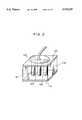
- FIG. 1is a view of the first embodiment of a semiconductor device constructed in accordance with the present invention.
- FIG. 2is a view of the second embodiment of a semiconductor device constructed in accordance with the present invention.
- FIG. 3is a sectional view of the third embodiment of a semiconductor device constructed in accordance with the present invention.
- FIG. 4is a view showing a conductor layout in the present invention.
- FIG. 5is a view showing another conductor layout in the present invention.
- FIG. 6is a view showing still another conductor layout in the present invention.
- FIG. 7is a view showing a further conductor layout in the present invention.
- FIG. 8is a view showing a further conductor layout in the present invention.
- FIG. 9Ais a view showing a conductor layout
- FIG. 9Bis a view showing another conductor layout
- FIG. 9Cis a view showing still another conductor layout.
- FIG. 10Ais a sectional view showing the structure of the fourth embodiment of a semiconductor device constructed in accordance with the present invention and FIG. 10B is a plan view showing the positional relationship between various parts in the structure of FIG. 10A.
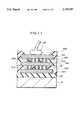
- FIG. 11is a sectional view of a modification of the fourth embodiment.
- FIG. 12is a sectional view of another modification of the fourth embodiment.
- FIG. 13is a sectional view showing the details of a semiconductor device constructed in accordance with the present invention.
- FIG. 14is a view showing the layouts of a bonding pad and internal circuit in a semiconductor chip.
- FIG. 15is a view illustrating a first step for forming the structure of FIG. 13.
- FIG. 16is a view illustrating a second step for forming the structure of FIG. 13.
- FIG. 17is a view illustrating a third step for forming the structure of FIG. 13.
- FIG. 18is a view illustrating a fourth step for forming the structure of FIG. 13.
- FIG. 19is a view illustrating a fifth step for forming the structure of FIG. 13.
- FIG. 20is a view illustrating a sixth step for forming the structure of FIG. 13.
- FIG. 21Ais a view of a conductor layer embedded in a through hole that is too large and FIG. 21B is a view of a conductor layer embedded in a suitable through hole.
- FIGS. 22A and 22Bare views used to illustrate problems raised when a through-hole is formed through an isotropic etching.
- FIGS. 23A, 23B and 23Care views used to illustrate different bondabilities in various electrode structures.
- FIG. 24is a view used to illustrate the problem in the structure of FIG. 23B.
- FIG. 25is a view used to illustrate advantages in the structure of FIG. 23C.
- FIG. 26is a view used to illustrate the problems that have been bared by the inventor prior to the present invention.
- FIGS. 27A and 27Bare views used to illustrate problems in the prior art.
- FIG. 1is a view of the first embodiment of a semiconductor device constructed in accordance with the present invention.
- the structure shown in FIG. 1comprises upper and lower electrode layers 100, 110 and an interlayer insulation film 130 between the upper and lower electrode layers.
- the central portion of the interlayer insulation film 130includes a through hole formed therethrough, into which an interlayer connection conductor 120 is embedded.
- the structurealso comprises a bonding wire 140 having a ball-like portion which is connected to the upper electrode layer 100 to cover the overall embedded conductor 120.
- the embedded metal 120will not be adversely affected by moisture entering the structure along the bonding wire 140.
- FIG. 2is a view of the second embodiment of a semiconductor device constructed in accordance with the present invention.
- the second embodimentis characterized by that further interlayer connection conductors 121 and 122 are disposed around the interlayer connection conductor 120 shown in FIG. 1.
- These conductors 120-122function not only to electrically connect the upper and lower electrode layers 100, 110, but also to provide a support between the upper and lower electrode layers 100, 110. Therefore, any crack will not be easily created in the interlayer insulation film 130 on bonding.
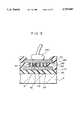
- FIG. 3is a view of the third embodiment of a semiconductor device constructed in accordance with the present invention.
- the third structureincludes a semiconductor substrate 10, a SiO 2 film 20 formed over the semiconductor substrate 10 and a double-layer wiring structure formed on the SiO 2 film 20.
- the double-layer wiring structureincludes upper and lower electrode layers 100, 110, a plurality of interlayer connection conductors 40-45, an interlayer insulation film 60 and another interlayer insulation film 70.
- the upper electrode layer 100is connected to the bonding wire 140.
- Through holes into which the interlayer connection conductors 40-45 are embeddedare required to have a sufficient diameter to completely receive the respective conductor, which is equal to about 1 ⁇ m.
- FIG. 21Ashows a through hole 6000 that is too large. If a conductor 4200 is deposited in such a through hole 6000 with the whole surface thereof being etched, the conductor 4200 will remain in only a part of the through-hole.
- the through hole 6000is substantially completely filled with the conductor 4200.
- the top face of the conductor 4200has the same height with the top face of the interlayer insulation film 20.
- the multi-layered electrode structurecan be more flattened.
- the through holemust be formed only by using anisotropic etching process such as Reactive Ion Etching (RIE). If through holes 7300 and 7200 are formed by using a combination of isotropic and anisotropic etchings as shown in FIG. 22A, the resulting multi-layered structure will have steep inclination as shown in FIG. 22B. Such a structure is not practicable.
- anisotropic etching processsuch as Reactive Ion Etching (RIE).
- the experimentsused three types of bonding pad structures which are shown in FIGS. 23A, 23B and 23C.
- the structure of FIG. 23Ai.e., the structure 3 in Table 1 is subjected to no peeling and has the highest strength against bonding impact.
- the structure of FIG. 23C according to the present invention(i.e., the structure 2 in Table 1) provides support columns 9500a, 9500b formed by conductors to absorb the bonding impact, as shown in FIG. 25.
- a crack lesstends to be created in the interlayer insulation film (e.g., CVDSiO 2 film).
- the bondabilitycan be enhanced. More particularly, the distortion of the silicon oxide film having its hardness higher than that of the metal wiring layer is suppressed to reduce the creation of cracks in the silicon oxide film. This is effective against the pad peeling and enhances the bondability.
- interlayer connection conductorse.g., planar pattern
- the layout densitycan be increased. Since the bonding impact is evenly absorbed by the respective conductors, a crack less tends to be created in the interlayer insulation film.
- the interlayer connection conductorscan be disposed with a further increased density.
- any redundancy in the layoutcan be avoided. Since the bonding impact is highest at the center of the bonding pad electrode, the bondability can be further improved by forming more through-holes in the center of the bonding pad electrode.
- groovesmay be formed so that conductors 94, 95 and 96 are embedded in the grooves.
- the conductors 94, 95 and 96function as walls for preventing any moisture from entering through the periphery of the semiconductor chip. Therefore, the moisture will not reach conductors 97, 98 and 99 that are located within the inner area surrounded by the grooves. This prevents corrosion.
- the conductors 94-99are covered with the ball-like portion of the bonding wire 140 as shown in FIG. 7, the conductors are also protected from the moisture entering along the bonding wire 140.
- groovesmay be formed in concentric circles around a through hole.
- Conductors 102, 103 and 104may be embedded into the grooves and through hole.
- the double-groove layoutcan reliably prevent the moisture from entering the semiconductor device.
- Conductorsmay be disposed in such a layout as shown in FIG. 9C.
- the layout of FIG. 9Cis provided from a combination of the groove layouts shown in FIGS. 9A and 9B.
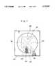
- FIG. 10Ais a plan view of the fourth embodiment of a semiconductor device constructed in accordance with the present invention while FIG. 10B is a view showing the planar positional relationship between the primary parts in the structure of FIG. 10A.
- the structure of FIG. 10Ahas a three-layer electrode structure which comprises a top electrode layer 510, an intermediate electrode layer 530 and a bottom electrode layer 550.
- the top and intermediate electrode layers 510, 530are connected to each other through interlayer connection conductors 561-563 while the intermediate and bottom electrode layers 530, 550 are connected to each other through inter-layer connection conductors 571-573.
- each of the top, intermediate and bottom electrode layers 510, 530, 550has a lateral extension in a given direction so as to function as a connection wire to the internal circuit.
- the present inventionis not limited to such an arrangement, but may have only one extension usable as a leading wire. Even if the top electrode layer has an extension functioning as a leading wire, the interlayer connection conductors 561-563 are required to ensure the good bonding.
- the number of interlayer connection conductorsmay be increased, if necessary, as shown in FIG. 11.
- interlayer connection conductors (606 and so on) in an interlayer insulation film 520are disposed to be perfectly aligned with the respective interlayer connection conductors (616 and so on) in an interlayer insulation film 540. This provides the maximum mechanical strength. In some cases, however, interlayer connection conductors (586 and so on) may be slightly offset from interlayer connection conductors (596 and so on) with partial overlaps, as shown in FIG. 12.
- the bonding padsare generally arranged along the peripheral edges of the semiconductor chip, as shown in FIG. 14.
- the present inventioncan increase the layout density of the bonding pads.
- FIGS. 13-20A method of making a semiconductor device according to the present invention will now be described with reference to FIGS. 13-20.
- FIG. 13shows the details of such a guard ring 3000, bonding pads 3100 and internal circuit 3200 as shown in FIG. 14.
- an electronic circuit using MOS transistorsis formed by forming gate electrodes 1580 and 1570 of polysilicon or the like and diffusion layers of impurity 1560, 1550, 1540, 1520 and 1500 on a semiconductor substrate 10.
- contact holesare formed in an insulation film 20. Titanium (Ti) film 4000 and titanium nitride (TiN) film 4100 are sequentially deposited on the insulation film 20 through the overall surface thereof. The titanium (Ti) film functions to reduce the contact resistance while the titanium nitride (TiN) film functions to facilitate the embedment of tungsten (W) into the contact holes in the following step.
- reference numerals 1561, 1530 and 1510designate titanium silicide (TiSi) layers.
- a tungsten (W) layer 5000is then formed, as shown in FIG. 16.
- the overall surface of the tungsten layer 5000is etched through RIE to embed the tungsten material into the contact holes, as shown in FIG. 17.
- embedded tungsten layers 4200a, 4200b and 4200care formed.
- Chlorine gasis used in the RIE performed to the tungsten layers.
- the chlorine gasis a cause wherein the aluminum wiring is corroded.
- the method of the present inventionforms the bonding pad at the same time when the multi-layered wiring structure in the internal circuit is formed. Therefore, the chlorine gas will not corrode the electrodes in the bonding pad. This improves the reliability in IC chips.
- titanium nitride (TiN) layersare stackedly formed and worked through the conventional photolithography to form such electrodes as shown by 1210 and 1212; 110 and 112; and 1110 and 1112 in FIG. 18.
- the titanium nitride (TiN) filmfunctions to prevent the reflection of exposure light, that is, as a reflection preventing layer.
- FIG. 19An interlayer insulation film 60 is then formed and through holes are selectively formed through the interlayer insulation film 60, as shown in FIG. 19.
- the same production process as shown in FIGS. 15-18is made to form a second electrode layer.
- reference numerals 4000d, 4000e and 4000fdenote titanium (Ti) films; 4100d, 4100e and 4100f titanium nitride (TiN) films; 4200d, 4200e and 4200h tungsten (W) layers; 1200, 100 and 1100 aluminum (Al) electrodes; and 1202, 102, 1102 reflection preventing layers of titanium nitride (TiN) film.
- a final protection film 70is then formed.
- the final protection film 70is selectively formed with openings each for a bonding pad.
- a bonding wire 140is then connected.
- a given potentialis applied to a diffusion layer 1500 to maintain a guard ring (which is formed by the aluminum electrodes 1110, 1100 and so on) at a given potential.
- the guard ringcan repel an ionic water to prevent moisture from entering through the outer periphery of the semiconductor chip as shown by arrow in FIG. 13.
- the conductor embedded into the through hole 2000D directly below the bonding wire 140will not be adversely affected by the moisture moved along the bonding wire 140 as shown by arrow in FIG. 13. Therefore, the bonding pad can be electrically connected to the other wiring layers in the reliable manner.
- the bonding areacan be reliably ensured to arrange the bonding pads with an increased density.
- reference numerals 2000A, 2000D and 2000Gdesignate through-holes while reference numerals 2000B, 2000F and 2000H denote contact holes.
- the present inventionmay be similarly applied to any other application such as a substrate using a thin film in a liquid crystal device or the like, in addition to monolithic IC.
- the external connectionis not limited to the bonding wire, but may be in the form of tape carrier or the like.
Landscapes
- Engineering & Computer Science (AREA)
- Computer Hardware Design (AREA)
- Microelectronics & Electronic Packaging (AREA)
- Power Engineering (AREA)
- Manufacturing & Machinery (AREA)
- Internal Circuitry In Semiconductor Integrated Circuit Devices (AREA)
- Wire Bonding (AREA)
Abstract
Description
The present invention relates to a semiconductor device and a method of making the semiconductor device, and particularly to an electrode for connecting IC chips to an external connecting terminal such as a bonding wire, and a method of making such an electrode.
FIG. 23A shows the multi-layered wiring structure of a bonding pad which was studied by the inventor prior to the present invention.
The bonding pad includes asemiconductor substrate 10 covered with an oxide film (SiO2 film) 9000. The bonding pad also includes aninterlayer insulation film 9200 having an opening which is formed by using both the isotropic and anisotropic etchings and first andsecond electrode layers
The other bonding pads of the prior art are shown in FIGS. 27A and 27B.
The structure of FIG. 27A is disclosed in Japanese Patent Application Laid-Open No. Sho 61-78151. To reduce a step in asecond electrode layer 6, such a structure includes a through hole 7 formed therethrough on the outer side. Thesecond electrode layer 6 is connected to afirst electrode layer 5 through the through hole.
In FIG. 27A,reference numeral 1 denotes a semiconductor substrate; 2 an oxide film (SIO2); 3 an interlayer insulation film; 4 a final passivation film; and 140 a bonding wire.
The structure of FIG. 27B is described in Japanese Patent Application Laid-Open No. Hei 1-130545.
The structure of FIG. 27B includes analuminum electrode layer 14 connected to thebonding wire 140 and abypass metal layer 16 located below thealuminum electrode layer 14 and connected thereto through abarrier metal layer 13. Even if thealuminum electrode layer 14 is corroded by moisture entering the semiconductor device, thebypass metal layer 16 can maintain the semiconductor device at its normal operation.
The inventor has studied the above prior art from various viewpoints. As a result, the following problems (1)-(3) emerged.
(1) If a three-layer electrode structure is formed using such a technique as shown in FIG. 23A, the aluminum wiring may be disconnected or corroded. This raises a problem in that the bonding area is reduced.
More particularly, when the first, second andthird electrode layers chain line 9500 in FIG. 26 has an increased risk of disconnecting the wiring.
As shown by arrow in FIG. 26, the aluminum electrodes are also easily corroded by moisture entering along thebonding wire 140 or from the outer periphery of the semiconductor chip.
When the semiconductor device is multi-layered, the bonding area is further reduced. More particularly, the dotted lines P1, P2 and P3 in FIG. 26 indicate boundaries of bonding areas on the electrode layers 9010, 9110 and 9310, respectively. When the electrodes are multi-layered, the area of the lowest electrode layer must be necessarily increased to secure its bonding area. It is thus difficult to form the bonding pad with an increased density.
(2) The structure of FIG. 27A has its reduced inter-layer steps. However, the area occupied by the electrodes will increase in the presence of theelectrode 5 on the outer side of the area connected to thebonding wire 140. It is also difficult to form the bonding pad with an increased density.
(3) The structure of FIG. 27B will have increased steps if the electrodes are further multi-layered. The area occupied by the bonding pad is increased since the electrodes extend in the lateral direction. This also makes the formation of high-density bonding pad difficult.
It is therefore an object of the present invention to provide a semiconductor device having a bonding pad, that is, its external connection terminal areas which can be formed with an increased density and having an improved reliability.
Another object of the present invention is to provide a method of effectively making such a semiconductor device.
In one preferred embodiment of a semiconductor device according to the present invention, a semiconductor device comprises upper and lower electrode layers and an inter-layer insulation film therebetween, the inter-layer insulation film including a through hole formed therethrough at given locations. The through hole includes an interlayer connection conductor embedded therein. Preferably, the ball-like portion of a bonding wire is connected to the upper electrode layer such that the ball-like portion perfectly covers the embedded conductor.
Such a structure has no step. Thus, the bonding areas can be more easily ensured to facilitate the formation of multi-layer structure. Furthermore, the embedded metal will not be adversely affected by moisture entering along the bonding wire.
The external connection terminals may be formed by any of various materials such as bump electrodes, film carriers. The present invention can be broadly applied as a connection technique for these terminals. It is particularly important to secure a desired bonding area and to provide any measure against larger pressing and separating forces if the connection is made using the bonding wire. In view of improvement of the reliability, the present invention is effective.
In another preferred embodiment, the multi-layered wiring structure of the bonding pad is preferably formed through a method of producing a multi-layered wiring structure that defines an internal circuit.
In still another preferred embodiment, the bonding pad may be formed by a multi-layered structure including three or more layers, using the structure that includes interlayer connection conductors each embedded into the respective one of through holes.
In a further preferred embodiment, the through-holes may be replaced by grooves into each of which an inter-layer connection conductor is embedded. If the plane configuration in the grooves is modified, moisture can be more effectively prevented from entering the semiconductor device through the outer periphery of the IC chip.
In a further preferred embodiment, it is desirable that a plurality of embedded conductor layers are disposed in a matrix. The configuration of the matrix may be of any of various forms such as circle.
In a further preferred embodiment, a guard ring is preferably formed along the outer periphery of the IC chip to further increase the prevention of moisture from entering the semiconductor device. It is desirable that the guard ring is maintained at a given potential.
In one preferred embodiment of a semiconductor device making method according the present invention, the multi-layered wiring structure of the internal circuit is formed through the same process as forming the multi-layered bonding pad and so on. The method comprises the steps of forming through holes in the insulation film and embedding conductor layers in the through holes.
Thus, the bonding pad and the like may be formed through the well-known VLSI making technique in which a metal or other conductor is embedded in a fine through hole.
In another preferred embodiment of the method according to the present invention, the guard ring is produced at the same time when the multi-layered wiring structure is formed.
FIG. 1 is a view of the first embodiment of a semiconductor device constructed in accordance with the present invention.
FIG. 2 is a view of the second embodiment of a semiconductor device constructed in accordance with the present invention.
FIG. 3 is a sectional view of the third embodiment of a semiconductor device constructed in accordance with the present invention.
FIG. 4 is a view showing a conductor layout in the present invention.
FIG. 5 is a view showing another conductor layout in the present invention.
FIG. 6 is a view showing still another conductor layout in the present invention.
FIG. 7 is a view showing a further conductor layout in the present invention.
FIG. 8 is a view showing a further conductor layout in the present invention.
FIG. 9A is a view showing a conductor layout; FIG. 9B is a view showing another conductor layout; and FIG. 9C is a view showing still another conductor layout.
FIG. 10A is a sectional view showing the structure of the fourth embodiment of a semiconductor device constructed in accordance with the present invention and FIG. 10B is a plan view showing the positional relationship between various parts in the structure of FIG. 10A.
FIG. 11 is a sectional view of a modification of the fourth embodiment.
FIG. 12 is a sectional view of another modification of the fourth embodiment.
FIG. 13 is a sectional view showing the details of a semiconductor device constructed in accordance with the present invention.
FIG. 14 is a view showing the layouts of a bonding pad and internal circuit in a semiconductor chip.
FIG. 15 is a view illustrating a first step for forming the structure of FIG. 13.
FIG. 16 is a view illustrating a second step for forming the structure of FIG. 13.
FIG. 17 is a view illustrating a third step for forming the structure of FIG. 13.
FIG. 18 is a view illustrating a fourth step for forming the structure of FIG. 13.
FIG. 19 is a view illustrating a fifth step for forming the structure of FIG. 13.
FIG. 20 is a view illustrating a sixth step for forming the structure of FIG. 13.
FIG. 21A is a view of a conductor layer embedded in a through hole that is too large and FIG. 21B is a view of a conductor layer embedded in a suitable through hole.
FIGS. 22A and 22B are views used to illustrate problems raised when a through-hole is formed through an isotropic etching.
FIGS. 23A, 23B and 23C are views used to illustrate different bondabilities in various electrode structures.
FIG. 24 is a view used to illustrate the problem in the structure of FIG. 23B.
FIG. 25 is a view used to illustrate advantages in the structure of FIG. 23C.
FIG. 26 is a view used to illustrate the problems that have been bared by the inventor prior to the present invention.
FIGS. 27A and 27B are views used to illustrate problems in the prior art.
(1) First Embodiment
FIG. 1 is a view of the first embodiment of a semiconductor device constructed in accordance with the present invention.
The structure shown in FIG. 1 comprises upper and lower electrode layers 100, 110 and aninterlayer insulation film 130 between the upper and lower electrode layers. The central portion of theinterlayer insulation film 130 includes a through hole formed therethrough, into which aninterlayer connection conductor 120 is embedded. The structure also comprises abonding wire 140 having a ball-like portion which is connected to theupper electrode layer 100 to cover the overall embeddedconductor 120.
Such a structure will not create any step. Therefore, the bonding area can be easily ensured to facilitate a further multi-layered structure.
The embeddedmetal 120 will not be adversely affected by moisture entering the structure along thebonding wire 140.
(2) Second Embodiment
FIG. 2 is a view of the second embodiment of a semiconductor device constructed in accordance with the present invention.
The second embodiment is characterized by that furtherinterlayer connection conductors interlayer connection conductor 120 shown in FIG. 1.
These conductors 120-122 function not only to electrically connect the upper and lower electrode layers 100, 110, but also to provide a support between the upper and lower electrode layers 100, 110. Therefore, any crack will not be easily created in theinterlayer insulation film 130 on bonding.
(3) Third Embodiment
FIG. 3 is a view of the third embodiment of a semiconductor device constructed in accordance with the present invention.
The third structure includes asemiconductor substrate 10, a SiO2 film 20 formed over thesemiconductor substrate 10 and a double-layer wiring structure formed on the SiO2 film 20. The double-layer wiring structure includes upper and lower electrode layers 100, 110, a plurality of interlayer connection conductors 40-45, aninterlayer insulation film 60 and anotherinterlayer insulation film 70. Theupper electrode layer 100 is connected to thebonding wire 140.
Through holes into which the interlayer connection conductors 40-45 are embedded are required to have a sufficient diameter to completely receive the respective conductor, which is equal to about 1 μm.
For example, FIG. 21A shows a throughhole 6000 that is too large. If aconductor 4200 is deposited in such a throughhole 6000 with the whole surface thereof being etched, theconductor 4200 will remain in only a part of the through-hole.
If the diameter of a through-hole is smaller in some extent as shown in FIG. 21B, the throughhole 6000 is substantially completely filled with theconductor 4200. The top face of theconductor 4200 has the same height with the top face of theinterlayer insulation film 20. Thus, the multi-layered electrode structure can be more flattened.
The through hole must be formed only by using anisotropic etching process such as Reactive Ion Etching (RIE). If throughholes
Experiments have showed the fact that the structure of the present invention shown in FIG. 3 is superior in bondability.
The experiments used three types of bonding pad structures which are shown in FIGS. 23A, 23B and 23C.
The experiments were carried out by applying a given load to the upper electrode layers connected to the respective bonding wires and then pulling the bonding wires to check whether or not peeling of bonding pad was created. The results of these experiments are shown in Table
TABLE 1 ______________________________________ Number of Peelings in Different Pad Structures Wafer No. #01 #02 #03 #04 Total ______________________________________Structure 1 2/16 2/16 3/16 2/16 9/64Structure 2 0/16 0/16 2/16 0/16 2/64Structure 3 0/16 0/16 0/16 0/16 0/64 ______________________________________
In Table 1, thestructure 1 corresponds to that of FIG. 23B; thestructure 2 corresponds to that of FIG. 23C; and thestructure 3 corresponds to that of FIG. 23A.
As will be apparent from Table 1, the structure of FIG. 23A (i.e., thestructure 3 in Table 1) is subjected to no peeling and has the highest strength against bonding impact.
On the other hand, all the wafers according to the structure of FIG. 23B (i.e., thestructure 1 in Table 1) are subjected to pad peeling and has the lowest strength with variety.
This is believed to be because a crack is likely to be created in a hard interlayer insulation film (e.g., CVDSiO2 film) with the crack promoting the pad peeling.
The structure of FIG. 23C according to the present invention (i.e., thestructure 2 in Table 1) providessupport columns
The layout of interlayer connection conductors (e.g., planar pattern) will be described below.
When the interlayer connection conductors 41-46 and so on are orderly disposed into a matrix as shown in FIG. 4, the layout density can be increased. Since the bonding impact is evenly absorbed by the respective conductors, a crack less tends to be created in the interlayer insulation film.
When the matrix includes conductors 80-86 in odd number lines and conductors 87-92 in even number lines with the conductors in the adjacent lines being staggered as shown in FIG. 5, the interlayer connection conductors can be disposed with a further increased density.
When the interlayer connection conductors are disposed into concentric circles for the ball-like configuration of the bonding wire as shown in FIG. 6, any redundancy in the layout can be avoided. Since the bonding impact is highest at the center of the bonding pad electrode, the bondability can be further improved by forming more through-holes in the center of the bonding pad electrode.
As shown in FIG. 7, grooves may be formed so thatconductors conductors conductors
Since the conductors 94-99 are covered with the ball-like portion of thebonding wire 140 as shown in FIG. 7, the conductors are also protected from the moisture entering along thebonding wire 140.
As shown in FIG. 8, furthermore, grooves may be formed in concentric circles around a through hole.Conductors
Conductors may be disposed in such a layout as shown in FIG. 9C. The layout of FIG. 9C is provided from a combination of the groove layouts shown in FIGS. 9A and 9B.
(4) Fourth Embodiment
FIG. 10A is a plan view of the fourth embodiment of a semiconductor device constructed in accordance with the present invention while FIG. 10B is a view showing the planar positional relationship between the primary parts in the structure of FIG. 10A.
The structure of FIG. 10A has a three-layer electrode structure which comprises atop electrode layer 510, anintermediate electrode layer 530 and abottom electrode layer 550. The top and intermediate electrode layers 510, 530 are connected to each other through interlayer connection conductors 561-563 while the intermediate and bottom electrode layers 530, 550 are connected to each other through inter-layer connection conductors 571-573.
In the structure of FIG. 10A, each of the top, intermediate and bottom electrode layers 510, 530, 550 has a lateral extension in a given direction so as to function as a connection wire to the internal circuit. However, the present invention is not limited to such an arrangement, but may have only one extension usable as a leading wire. Even if the top electrode layer has an extension functioning as a leading wire, the interlayer connection conductors 561-563 are required to ensure the good bonding.
The number of interlayer connection conductors may be increased, if necessary, as shown in FIG. 11.
The structure of FIG. 11 is characterized by that interlayer connection conductors (606 and so on) in aninterlayer insulation film 520 are disposed to be perfectly aligned with the respective interlayer connection conductors (616 and so on) in aninterlayer insulation film 540. This provides the maximum mechanical strength. In some cases, however, interlayer connection conductors (586 and so on) may be slightly offset from interlayer connection conductors (596 and so on) with partial overlaps, as shown in FIG. 12.
As shown in FIG. 14, the bonding pads are generally arranged along the peripheral edges of the semiconductor chip, as shown in FIG. 14. The present invention can increase the layout density of the bonding pads.
(5) Fifth Embodiment
A method of making a semiconductor device according to the present invention will now be described with reference to FIGS. 13-20.
FIG. 13 shows the details of such aguard ring 3000,bonding pads 3100 andinternal circuit 3200 as shown in FIG. 14.
A process for making the structure of FIG. 13 will be described in sequence.
As shown in FIG. 15, first, an electronic circuit using MOS transistors is formed by forminggate electrodes impurity semiconductor substrate 10. Second, contact holes are formed in aninsulation film 20. Titanium (Ti)film 4000 and titanium nitride (TiN)film 4100 are sequentially deposited on theinsulation film 20 through the overall surface thereof. The titanium (Ti) film functions to reduce the contact resistance while the titanium nitride (TiN) film functions to facilitate the embedment of tungsten (W) into the contact holes in the following step. In FIG. 15,reference numerals
A tungsten (W)layer 5000 is then formed, as shown in FIG. 16.
Subsequently, the overall surface of thetungsten layer 5000 is etched through RIE to embed the tungsten material into the contact holes, as shown in FIG. 17. Thus, embeddedtungsten layers
Chlorine gas is used in the RIE performed to the tungsten layers. The chlorine gas is a cause wherein the aluminum wiring is corroded. To avoid such a problem, the method of the present invention forms the bonding pad at the same time when the multi-layered wiring structure in the internal circuit is formed. Therefore, the chlorine gas will not corrode the electrodes in the bonding pad. This improves the reliability in IC chips.
Subsequently, aluminum (Al) and titanium nitride (TiN) layers are stackedly formed and worked through the conventional photolithography to form such electrodes as shown by 1210 and 1212; 110 and 112; and 1110 and 1112 in FIG. 18. The titanium nitride (TiN) film functions to prevent the reflection of exposure light, that is, as a reflection preventing layer.
Aninterlayer insulation film 60 is then formed and through holes are selectively formed through theinterlayer insulation film 60, as shown in FIG. 19. The same production process as shown in FIGS. 15-18 is made to form a second electrode layer. In FIG. 19,reference numerals
As shown in FIG. 20, afinal protection film 70 is then formed. Thefinal protection film 70 is selectively formed with openings each for a bonding pad.
Abonding wire 140 is then connected. A given potential is applied to adiffusion layer 1500 to maintain a guard ring (which is formed by thealuminum electrodes
The conductor embedded into the throughhole 2000D directly below thebonding wire 140 will not be adversely affected by the moisture moved along thebonding wire 140 as shown by arrow in FIG. 13. Therefore, the bonding pad can be electrically connected to the other wiring layers in the reliable manner.
Even if the multi-layered structure has more layers, no step will be created in the structure. In other words, the flatness in the bonding pad can be maintained even if the metal electrodes are formed into more layers. Therefore, the wiring will not be disconnected. Furthermore, the bonding area can be reliably ensured to arrange the bonding pads with an increased density.
In FIG. 13,reference numerals reference numerals
The present invention may be similarly applied to any other application such as a substrate using a thin film in a liquid crystal device or the like, in addition to monolithic IC. The external connection is not limited to the bonding wire, but may be in the form of tape carrier or the like.
Claims (11)
1. A semiconductor device having a multi-layered wiring structure comprising:
a first conductor layer connected to an external connection terminal;
a second conductor layer;
an electrical insulation layer interposed between said first and second conductor layers; and
a third conductor layer embedded in a through hole selectively formed through said electrical insulation layer, said third conductor layer electrically connecting said first conductor layer to said second conductor layer;
wherein said third conductor layer is filled in said through hole, the height of the top and bottom of said third conductor layer being substantially equal to the height of the top and bottom of said electrical insulation layer and said third conductor layer is harder than said first and second conductor layers.
2. The semiconductor device as defined in claim 1 wherein a surface of said third conductor layer contacting said first conductor layer is covered with said external connection terminal.
3. The semiconductor device as defined in claim 1 wherein said first and second conductor layers contain aluminum as a chief component and wherein said third conductor layer contains tungsten as a chief component.
4. The semiconductor device as defined in claim 1, further comprising an internal circuit formed by a multi-layered wiring structure and wherein said first, second and third conductor layers, electrical insulation layer and through hole are formed through the same production process as forming said multi-layered wiring structure of said internal circuit.
5. The semiconductor device as defined in claim 1 wherein said external connection terminal is a bonding wire.
6. A semiconductor device having a multi-layered wiring structure comprising:
a first conductor layer connected to an external connection terminal;
a second conductor layer;
an electrical insulation layer interposed between said first and second conductor layers; and
a plurality of third conductor layers each embedded in one of a plurality of through holes selectively formed through said electrical insulation layer, said third conductor layers electrically connecting said first conductor layer to said second conductor layer;
wherein each of said third conductor layers is filled in the corresponding one of said through holes, the height of the top and bottom of the third conductor layer being substantially equal to the height of the top and bottom of said electrical insulation layer and said third conductor layers are arranged into a matrix; and
wherein a surface of at least one of said third conductor layers contacting said first conductor layer is covered with said external connection terminal.
7. The semiconductor device is defined in claim 6 wherein said third conductor layers are arranged into a plurality of lines forming a matrix of even number lines and odd number lines, the even number lines being staggered from the odd number lines in said matrix.
8. The semiconductor device as defined in claim 6 wherein said third conductor layers are arranged into concentric circles.
9. A semiconductor device having a multi-layered wiring structure comprising:
a first conductor layer connected to an external connection terminal;
a second conductor layer;
an electrical insulation layer interposed between said first and second conductor layers; and
a third conductor layer embedded into a groove selectively formed in said electrical insulation layer, said third conductor layer electrically connecting said first conductor layer to said second conductor layer;
wherein said third conductor layer is filled in said groove, the height of the top and bottom of said third conductor layer being substantially equal to the height of the top and bottom of said electrical insulation layer.
10. The semiconductor device as defined in claim 9,
wherein said third conductor layer embedded into said groove is formed into a closed configuration, said electrical insulation layer being partitioned into inner and outer portions about said closed configuration;
wherein said inner portion of said electrical insulation layer includes a through hole selectively formed therethrough, said through hole including a fourth conductor layer embedded thereinto and formed of the same material as in said third conductor layer; and
wherein said external connection terminal is connected to said first conductor layer to cover said fourth conductor layer.
11. A semiconductor device having a multi-layered wiring structure comprising:
a first conductor layer connected to an external connection terminal;
a second conductor layer;
a third conductor layer formed to have an overlap relative to said second conductor layer;
a first electrical insulation layer interposed between said first and second conductor layers;
a second electrical insulation layer interposed between said second and third conductor layers;
a fourth conductor layer embedded into a first through hole selectively formed through said first electrical insulation layer, said fourth conductor layer electrically connecting said first conductor layer to said second conductor layer; and
a fifth conductor layer embedded into a second through hole selectively formed through said second electrical insulation layer, said fifth conductor layer electrically connecting said second conductor layer to said third conductor layer;
a guard ring located at a position nearer an outer periphery of the semiconductor device than the position at which said external connection terminal is connected to the semiconductor device, said guard ring having a given potential;
wherein said fourth conductor layer is filled in said first through hole such that the height of the top and bottom of said fourth conductor layer is substantially equal to the height of the top and bottom of said first electrical insulation layer;
wherein said fifth conductor layer is filled in said second through hole such that the height of the top and bottom of said fifth conductor layer is substantially equal to the height of the top and bottom of said second electrical insulation layer; and
wherein said fourth and fifth conductor layers in said first and second through holes have an overlap.
Applications Claiming Priority (4)
| Application Number | Priority Date | Filing Date | Title |
|---|---|---|---|
| JP3270795 | 1995-02-21 | ||
| JP7-032707 | 1995-02-21 | ||
| JP8-052273 | 1996-02-15 | ||
| JP8052273AJPH08293523A (en) | 1995-02-21 | 1996-02-15 | Semiconductor device and manufacturing method thereof |
Publications (1)
| Publication Number | Publication Date |
|---|---|
| US5739587Atrue US5739587A (en) | 1998-04-14 |
Family
ID=26371289
Family Applications (1)
| Application Number | Title | Priority Date | Filing Date |
|---|---|---|---|
| US08/603,166Expired - LifetimeUS5739587A (en) | 1995-02-21 | 1996-02-20 | Semiconductor device having a multi-latered wiring structure |
Country Status (2)
| Country | Link |
|---|---|
| US (1) | US5739587A (en) |
| JP (1) | JPH08293523A (en) |
Cited By (109)
| Publication number | Priority date | Publication date | Assignee | Title |
|---|---|---|---|---|
| WO1999017348A1 (en)* | 1997-09-30 | 1999-04-08 | Intel Corporation | Metal staples to prevent interlayer delamination |
| US5923088A (en)* | 1996-08-22 | 1999-07-13 | Taiwan Semiconductor Manufacturing Company, Ltd. | Bond pad structure for the via plug process |
| US5939790A (en)* | 1996-04-09 | 1999-08-17 | Altera Corporation | Integrated circuit pad structures |
| US5959360A (en)* | 1998-05-22 | 1999-09-28 | United Microelectronics Corp. | Interconnect structure employing equivalent resistance paths to improve electromigration resistance |
| US5963831A (en)* | 1998-05-22 | 1999-10-05 | United Microelectronics Corp. | Method of making an interconnect structure employing equivalent resistance paths to improve electromigration resistance |
| US5969421A (en)* | 1997-11-18 | 1999-10-19 | Lucent Technologies Inc. | Integrated circuit conductors that avoid current crowding |
| US5986343A (en)* | 1998-05-04 | 1999-11-16 | Lucent Technologies Inc. | Bond pad design for integrated circuits |
| US6020647A (en)* | 1998-12-18 | 2000-02-01 | Vlsi Technology, Inc. | Composite metallization structures for improved post bonding reliability |
| US6028367A (en)* | 1999-05-07 | 2000-02-22 | Taiwan Semiconductor Manufacturing Company, Ltd. | Bonds pads equipped with heat dissipating rings and method for forming |
| US6087732A (en)* | 1998-09-28 | 2000-07-11 | Lucent Technologies, Inc. | Bond pad for a flip-chip package |
| US6100591A (en)* | 1998-05-25 | 2000-08-08 | Nec Corporation | Semiconductor device and method of fabricating the same |
| US6137178A (en)* | 1998-06-17 | 2000-10-24 | Siemens Aktiengesellschaft | Semiconductor metalization system and method |
| WO2000042659A3 (en)* | 1999-01-15 | 2000-11-23 | Broadcom Corp | System and method for esd protection |
| US6163075A (en)* | 1998-05-26 | 2000-12-19 | Nec Corporation | Multilayer wiring structure and semiconductor device having the same, and manufacturing method therefor |
| US6175156B1 (en)* | 1997-11-21 | 2001-01-16 | Mitsubishi Denki Kabushiki Kaisha | Semiconductor device with improved interconnection |
| US6181016B1 (en)* | 1999-06-08 | 2001-01-30 | Winbond Electronics Corp | Bond-pad with a single anchoring structure |
| US6191481B1 (en) | 1998-12-18 | 2001-02-20 | Philips Electronics North America Corp. | Electromigration impeding composite metallization lines and methods for making the same |
| WO2001045165A1 (en)* | 1999-12-16 | 2001-06-21 | Conexant Systems, Inc. | Bonding pad and support structure and method for their fabrication |
| US6313540B1 (en)* | 1998-12-25 | 2001-11-06 | Nec Corporation | Electrode structure of semiconductor element |
| US6313537B1 (en)* | 1997-12-09 | 2001-11-06 | Samsung Electronics Co., Ltd. | Semiconductor device having multi-layered pad and a manufacturing method thereof |
| US6316836B1 (en)* | 1998-05-27 | 2001-11-13 | Nec Corporation | Semiconductor device interconnection structure |
| US6320262B1 (en)* | 1997-12-05 | 2001-11-20 | Ricoh Company, Ltd. | Semiconductor device and manufacturing method thereof |
| US20010045669A1 (en)* | 2000-04-12 | 2001-11-29 | Zhongning Liang | Semiconductor device |
| US6365970B1 (en)* | 1999-12-10 | 2002-04-02 | Silicon Integrated Systems Corporation | Bond pad structure and its method of fabricating |
| US6426284B1 (en)* | 2000-03-20 | 2002-07-30 | Illinois Tool Works Inc. | Method of manufacturing wire bond pad |
| US6426680B1 (en) | 1999-05-26 | 2002-07-30 | Broadcom Corporation | System and method for narrow band PLL tuning |
| US6445039B1 (en) | 1998-11-12 | 2002-09-03 | Broadcom Corporation | System and method for ESD Protection |
| US6448641B2 (en)* | 1999-03-19 | 2002-09-10 | Industrial Technology Research Institute | Low-capacitance bonding pad for semiconductor device |
| US6448650B1 (en)* | 1998-05-18 | 2002-09-10 | Texas Instruments Incorporated | Fine pitch system and method for reinforcing bond pads in semiconductor devices |
| US6465337B1 (en)* | 1998-06-24 | 2002-10-15 | Samsung Electronics Co., Ltd. | Methods of fabricating integrated circuit bonding pads including intermediate closed conductive layers having spaced apart insulating islands therein |
| US6489228B1 (en)* | 1997-12-05 | 2002-12-03 | Stmicroelectronics S.R.L. | Integrated electronic device comprising a mechanical stress protection structure |
| US6495918B1 (en)* | 2000-09-05 | 2002-12-17 | Infineon Technologies Ag | Chip crack stop design for semiconductor chips |
| US20030011072A1 (en)* | 2001-06-28 | 2003-01-16 | Hiroyuki Shinogi | Semiconductor device and the manufacturing method thereof |
| US20030011073A1 (en)* | 2001-06-28 | 2003-01-16 | Hiroyuki Shinogi | Semiconductor device and the manufacturing method thereof |
| US6525609B1 (en) | 1998-11-12 | 2003-02-25 | Broadcom Corporation | Large gain range, high linearity, low noise MOS VGA |
| US6552433B1 (en) | 2001-05-17 | 2003-04-22 | Taiwan Semiconductor Manufacturing Company | Bond pads using mesh pattern via structures for protecting devices/circuits under I/O pads |
| US6552438B2 (en)* | 1998-06-24 | 2003-04-22 | Samsung Electronics Co. | Integrated circuit bonding pads including conductive layers with arrays of unaligned spaced apart insulating islands therein and methods of forming same |
| US20030234277A1 (en)* | 2002-06-25 | 2003-12-25 | Rajen Dias | Microelectronic device interconnects |
| KR100421043B1 (en)* | 2000-12-21 | 2004-03-04 | 삼성전자주식회사 | Integrated circuit bonding pads including conductive layers with arrays of unaligned spaced apart insulating islands therein |
| WO2003001595A3 (en)* | 2001-06-25 | 2004-05-27 | Koninkl Philips Electronics Nv | Electronic device |
| US6756675B1 (en)* | 1996-08-20 | 2004-06-29 | Seiko Epson Corporation | Semiconductor device and a method for making the same that provide arrangement of a connecting region for an external connecting terminal |
| US20040140565A1 (en)* | 2002-11-14 | 2004-07-22 | Stmicroelectronics Sa | Electrical connection device between two tracks of an integrated circuit |
| US6777815B2 (en)* | 2001-08-29 | 2004-08-17 | Via Technologies, Inc. | Configuration of conductive bumps and redistribution layer on a flip chip |
| US20050017368A1 (en)* | 2002-12-20 | 2005-01-27 | Atila Mertol | Multi-level redistribution layer traces for reducing current crowding in flipchip solder bumps |
| WO2005010988A1 (en)* | 2003-07-22 | 2005-02-03 | Infineon Technologies Ag | Electronic component with semiconductor chip and semiconductor wafer having contact pads, and method for the production thereof |
| US20050023692A1 (en)* | 2003-06-23 | 2005-02-03 | Takashi Matsunaga | Semiconductor apparatus including a radiator for diffusing the heat generated therein |
| US20050054188A1 (en)* | 2003-09-08 | 2005-03-10 | Renesas Technology Corp. | Semiconductor device and method of manufacturing the same |
| US6879049B1 (en)* | 1998-01-23 | 2005-04-12 | Rohm Co., Ltd. | Damascene interconnection and semiconductor device |
| US6885275B1 (en) | 1998-11-12 | 2005-04-26 | Broadcom Corporation | Multi-track integrated spiral inductor |
| US20050127529A1 (en)* | 2003-12-10 | 2005-06-16 | Taiwan Semiconductor Manufacturing Co., Ltd. | Structure and method for reinforcing a bond pad on a chip |
| US6921714B2 (en)* | 1998-10-01 | 2005-07-26 | Yamaha Corporation | Method for manufacturing a semiconductor device |
| US20050173801A1 (en)* | 2004-02-05 | 2005-08-11 | Matsushita Elec. Ind. Co. Ltd. | Semiconductor device |
| US20050189637A1 (en)* | 2004-02-17 | 2005-09-01 | Sanyo Electric Co., Ltd. | Semiconductor device and manufacturing method thereof |
| US20050194649A1 (en)* | 2004-02-12 | 2005-09-08 | Tomohiro Oki | Semiconductor chip and method for testing semiconductor chip |
| US6955981B2 (en) | 2002-09-13 | 2005-10-18 | Taiwan Semiconductor Manufacturing Company, Ltd. | Pad structure to prompt excellent bondability for low-k intermetal dielectric layers |
| US20050230847A1 (en)* | 2004-04-14 | 2005-10-20 | Jian-Hsing Lee | Bonding pad structure and method of forming the same |
| US20050258901A1 (en)* | 1998-11-12 | 2005-11-24 | Broadcom Corporation | System and method for linearizing a CMOS differential pair |
| US6985035B1 (en) | 1998-11-12 | 2006-01-10 | Broadcom Corporation | System and method for linearizing a CMOS differential pair |
| US7026225B1 (en)* | 2003-09-09 | 2006-04-11 | Advanced Micro Devices, Inc. | Semiconductor component and method for precluding stress-induced void formation in the semiconductor component |
| US7045903B2 (en)* | 2000-07-27 | 2006-05-16 | Texas Instruments Incorporated | Integrated power circuits with distributed bonding and current flow |
| US20060108691A1 (en)* | 2004-10-28 | 2006-05-25 | Sanyo Electric Co., Ltd. | Semiconductor device and manufacturing method of the same |
| US20060125015A1 (en)* | 2004-12-13 | 2006-06-15 | Broadcom Corporation | ESD protection for high voltage applications |
| US20060125118A1 (en)* | 2004-12-10 | 2006-06-15 | Elpida Memory, Inc. | Semiconductor device having a bonding pad structure including an annular contact |
| US20060152870A1 (en)* | 2005-01-07 | 2006-07-13 | Broadcom Corporation | ESD configuration for low parasitic capacitance I/O |
| US20060267222A1 (en)* | 2005-05-30 | 2006-11-30 | Fujitsu Limited | Semiconductor element and manufacturing method thereof |
| US20060267008A1 (en)* | 2005-05-27 | 2006-11-30 | Taiwan Semiconductor Manufacturing Company, Ltd. | Semiconductor bond pad structures and methods of manufacturing thereof |
| US20070001317A1 (en)* | 2005-07-04 | 2007-01-04 | Fujitsu Limited | Semiconductor device |
| US20070007655A1 (en)* | 2005-07-06 | 2007-01-11 | Yuichi Miyamori | Semiconductor device |
| US20070052068A1 (en)* | 2005-09-02 | 2007-03-08 | Koji Takemura | Semiconductor device |
| US20070080464A1 (en)* | 2005-10-12 | 2007-04-12 | Thomas Goebel | Support structures for semiconductor devices |
| WO2007064073A1 (en)* | 2005-12-02 | 2007-06-07 | Nepes Corporation | Bump with multiple vias for semiconductor package, method of fabrication method thereof, and semiconductor package using the same |
| US20070182001A1 (en)* | 2004-02-26 | 2007-08-09 | Renesas Technology Corp. | Semiconductor device |
| US7276435B1 (en)* | 2006-06-02 | 2007-10-02 | Freescale Semiconductor, Inc. | Die level metal density gradient for improved flip chip package reliability |
| KR100804392B1 (en) | 2005-12-02 | 2008-02-15 | 주식회사 네패스 | Semiconductor package and manufacturing method thereof |
| DE102006052202B3 (en)* | 2006-11-06 | 2008-02-21 | Infineon Technologies Ag | Semiconductor component has metal layer comprising coherent section, and other metal layer is arranged on coherent section of former metal layer, where latter metal layer is structured between layered regions |
| US20080042292A1 (en)* | 2006-08-18 | 2008-02-21 | Adkisson James W | Bond pad for wafer and package for cmos imager |
| US20080111250A1 (en)* | 2006-11-13 | 2008-05-15 | International Business Machines Corporation | Structure and method for enhancing resistance to fracture of bonding pads |
| US20080122100A1 (en)* | 2006-11-07 | 2008-05-29 | Taiwan Semiconductor Manufacturing Co., Ltd. | Novel bond pad design to minimize dielectric cracking |
| US20080132038A1 (en)* | 2004-10-26 | 2008-06-05 | Sanyo Electric Co., Ltd. | Semiconductor device and manufacturing method of the same |
| US20080160656A1 (en)* | 2007-01-03 | 2008-07-03 | International Business Machines Corporation | Addressable hierarchical metal wire test methodology |
| US20080174925A1 (en)* | 1999-01-15 | 2008-07-24 | Broadcom Corporation | System and method for ESD protection |
| US20080272499A1 (en)* | 2007-05-03 | 2008-11-06 | Teledyne Licensing, Llc | Through-wafer vias |
| US20090027137A1 (en)* | 2003-11-12 | 2009-01-29 | Fjelstad Joseph C | Tapered dielectric and conductor structures and applications thereof |
| US20090091019A1 (en)* | 2003-11-17 | 2009-04-09 | Joseph Charles Fjelstad | Memory Packages Having Stair Step Interconnection Layers |
| US20090124078A1 (en)* | 2005-03-10 | 2009-05-14 | Sanyo Electric Co., Ltd. | Method of manufacturing semiconductor device with through hole |
| US20090160066A1 (en)* | 2007-12-21 | 2009-06-25 | Junichi Ikeda | Semiconductor element, semiconductor device, and fabrication method thereof |
| US20090309232A1 (en)* | 2008-04-30 | 2009-12-17 | Stmicroelectronics (Crolles 2) Sas | Method of making connections in a back-lit circuit |
| US20090321871A1 (en)* | 2008-06-26 | 2009-12-31 | Wu-Te Weng | Chip Pad Resistant to Antenna Effect and Method |
| US7696823B2 (en) | 1999-05-26 | 2010-04-13 | Broadcom Corporation | System and method for linearizing a CMOS differential pair |
| US20100155958A1 (en)* | 2008-12-18 | 2010-06-24 | Samsung Electronics Co., Ltd. | Bonding pad structure and manufacturing method thereof |
| US20100176515A1 (en)* | 2009-01-12 | 2010-07-15 | Vanguard International Semiconductor Corporation | Contact pad supporting structure and integrated circuit |
| US20110139497A1 (en)* | 2009-12-14 | 2011-06-16 | Qualcomm Incorporated | Via Structure Integrated in Electronic Substrate |
| US20110175220A1 (en)* | 2010-01-20 | 2011-07-21 | Taiwan Semiconductor Manufacturing Company, Ltd. | Semiconductor device having conductive pads and a method of manufacturing the same |
| US20110272818A1 (en)* | 2010-05-10 | 2011-11-10 | Jeong Jong-Yeul | Semiconductor device for preventing crack in pad region and fabricating method thereof |
| CN102751255A (en)* | 2012-07-26 | 2012-10-24 | 上海宏力半导体制造有限公司 | Semiconductor bond pad structure, manufacturing method thereof and integrated circuit |
| US8405152B2 (en) | 1999-01-15 | 2013-03-26 | Broadcom Corporation | System and method for ESD protection |
| CN103579166A (en)* | 2012-07-26 | 2014-02-12 | 中芯国际集成电路制造(上海)有限公司 | Pad structure |
| US8728889B2 (en) | 2012-04-13 | 2014-05-20 | Samsung Electronics Co., Ltd. | Contact structure and manufacturing method thereof |
| US8736080B2 (en) | 2012-04-30 | 2014-05-27 | Apple Inc. | Sensor array package |
| US8981578B2 (en) | 2012-04-30 | 2015-03-17 | Apple Inc. | Sensor array package |
| CN105097741A (en)* | 2014-05-05 | 2015-11-25 | 中芯国际集成电路制造(上海)有限公司 | Pad structure and manufacturing method thereof |
| US20160055935A1 (en)* | 2013-03-25 | 2016-02-25 | Epcos Ag | Apparatus and Method for Establishing an Electrically Conductive and Mechanical Connection |
| US9478481B2 (en) | 2011-11-15 | 2016-10-25 | Rohm Co., Ltd. | Semiconductor device, method for manufacturing same, and electronic component |
| EP2953159A4 (en)* | 2013-02-01 | 2016-11-09 | Sii Semiconductor Corp | Semiconductor device |
| CN102751255B (en)* | 2012-07-26 | 2016-11-30 | 上海华虹宏力半导体制造有限公司 | Semiconductor bond pad structure and manufacture method thereof and integrated circuit |
| US20170040274A1 (en)* | 2014-10-16 | 2017-02-09 | Globalfoundries Inc. | Bond pad structure for low temperature flip chip bonding |
| US20190304847A1 (en)* | 2017-12-07 | 2019-10-03 | Micron Technology, Inc. | Apparatuses Having an Interconnect Extending from an Upper Conductive Structure, Through a Hole in Another Conductive Structure, and to an Underlying Structure |
| US20210376028A1 (en)* | 2018-07-02 | 2021-12-02 | Samsung Display Co., Ltd. | Display device |
| US20220246568A1 (en)* | 2021-01-29 | 2022-08-04 | Samsung Electronics Co., Ltd. | Semiconductor package including post |
Families Citing this family (15)
| Publication number | Priority date | Publication date | Assignee | Title |
|---|---|---|---|---|
| JPH11121458A (en) | 1997-10-21 | 1999-04-30 | Nec Kyushu Ltd | Semiconductor device |
| KR100319896B1 (en)* | 1998-12-28 | 2002-01-10 | 윤종용 | Bonding pad structure of semiconductor device and fabrication method thereof |
| US6232662B1 (en)* | 1998-07-14 | 2001-05-15 | Texas Instruments Incorporated | System and method for bonding over active integrated circuits |
| GB2364170B (en)* | 1999-12-16 | 2002-06-12 | Lucent Technologies Inc | Dual damascene bond pad structure for lowering stress and allowing circuitry under pads and a process to form the same |
| US8274160B2 (en) | 2003-08-21 | 2012-09-25 | Intersil Americas Inc. | Active area bonding compatible high current structures |
| JP2005116562A (en)* | 2003-10-02 | 2005-04-28 | Renesas Technology Corp | Semiconductor device |
| JP4596464B2 (en)* | 2005-03-17 | 2010-12-08 | 次世代半導体材料技術研究組合 | Semiconductor device |
| JP4646789B2 (en)* | 2005-12-02 | 2011-03-09 | パナソニック株式会社 | Semiconductor device |
| JP5280840B2 (en)* | 2006-03-31 | 2013-09-04 | 富士通株式会社 | Semiconductor device |
| JP2008016638A (en)* | 2006-07-06 | 2008-01-24 | Sony Corp | Semiconductor device |
| JP2008091632A (en)* | 2006-10-02 | 2008-04-17 | Manabu Bonshihara | Structure of external circuit connection section in semiconductor device and method of forming the same |
| JP2008248783A (en)* | 2007-03-30 | 2008-10-16 | Diamond Electric Mfg Co Ltd | Igniter |
| JP5262161B2 (en)* | 2008-02-14 | 2013-08-14 | カシオ計算機株式会社 | Semiconductor integrated circuit device |
| JP5994167B2 (en)* | 2011-11-15 | 2016-09-21 | ローム株式会社 | Semiconductor device, manufacturing method thereof, and electronic component |
| JP2013235127A (en)* | 2012-05-09 | 2013-11-21 | Seiko Epson Corp | Electro-optic device, method for manufacturing electro-optic device and electronic apparatus |
Citations (10)
| Publication number | Priority date | Publication date | Assignee | Title |
|---|---|---|---|---|
| JPS6178151A (en)* | 1984-09-25 | 1986-04-21 | Nec Corp | Semiconductor device |
| US4636832A (en)* | 1982-07-27 | 1987-01-13 | Tokyo Shibaura Denki Kabushiki Kaisha | Semiconductor device with an improved bonding section |
| JPH01130545A (en)* | 1987-11-17 | 1989-05-23 | Mitsubishi Electric Corp | Resin-sealed type semiconductor device |
| US5248903A (en)* | 1992-09-18 | 1993-09-28 | Lsi Logic Corporation | Composite bond pads for semiconductor devices |
| US5404046A (en)* | 1990-05-31 | 1995-04-04 | Canon Kabushiki Kaisha | Flat semiconductor wiring layers |
| US5463255A (en)* | 1992-03-30 | 1995-10-31 | Nec Corporation | Semiconductor integrated circuit device having an electrode pad including an extended wire bonding portion |
| US5475268A (en)* | 1994-06-13 | 1995-12-12 | Mitsubishi Denki Kabushiki Kaisha | Semiconductor device having an alignment mark |
| US5502337A (en)* | 1994-07-04 | 1996-03-26 | Mitsubishi Denki Kabushiki Kaisha | Semiconductor device structure including multiple interconnection layers with interlayer insulating films |
| US5539247A (en)* | 1992-12-15 | 1996-07-23 | Advanced Micro Devices, Incorporated | Selective metal via plug growth technology for deep sub-micrometer ULSI |
| US5621247A (en)* | 1995-02-20 | 1997-04-15 | Matsushita Electric Industrial Co., Ltd. | Memory device with tungsten and aluminum interconnects |
- 1996
- 1996-02-15JPJP8052273Apatent/JPH08293523A/enactivePending
- 1996-02-20USUS08/603,166patent/US5739587A/ennot_activeExpired - Lifetime
Patent Citations (10)
| Publication number | Priority date | Publication date | Assignee | Title |
|---|---|---|---|---|
| US4636832A (en)* | 1982-07-27 | 1987-01-13 | Tokyo Shibaura Denki Kabushiki Kaisha | Semiconductor device with an improved bonding section |
| JPS6178151A (en)* | 1984-09-25 | 1986-04-21 | Nec Corp | Semiconductor device |
| JPH01130545A (en)* | 1987-11-17 | 1989-05-23 | Mitsubishi Electric Corp | Resin-sealed type semiconductor device |
| US5404046A (en)* | 1990-05-31 | 1995-04-04 | Canon Kabushiki Kaisha | Flat semiconductor wiring layers |
| US5463255A (en)* | 1992-03-30 | 1995-10-31 | Nec Corporation | Semiconductor integrated circuit device having an electrode pad including an extended wire bonding portion |
| US5248903A (en)* | 1992-09-18 | 1993-09-28 | Lsi Logic Corporation | Composite bond pads for semiconductor devices |
| US5539247A (en)* | 1992-12-15 | 1996-07-23 | Advanced Micro Devices, Incorporated | Selective metal via plug growth technology for deep sub-micrometer ULSI |
| US5475268A (en)* | 1994-06-13 | 1995-12-12 | Mitsubishi Denki Kabushiki Kaisha | Semiconductor device having an alignment mark |
| US5502337A (en)* | 1994-07-04 | 1996-03-26 | Mitsubishi Denki Kabushiki Kaisha | Semiconductor device structure including multiple interconnection layers with interlayer insulating films |
| US5621247A (en)* | 1995-02-20 | 1997-04-15 | Matsushita Electric Industrial Co., Ltd. | Memory device with tungsten and aluminum interconnects |
Cited By (223)
| Publication number | Priority date | Publication date | Assignee | Title |
|---|---|---|---|---|
| US5939790A (en)* | 1996-04-09 | 1999-08-17 | Altera Corporation | Integrated circuit pad structures |
| US6756675B1 (en)* | 1996-08-20 | 2004-06-29 | Seiko Epson Corporation | Semiconductor device and a method for making the same that provide arrangement of a connecting region for an external connecting terminal |
| US5923088A (en)* | 1996-08-22 | 1999-07-13 | Taiwan Semiconductor Manufacturing Company, Ltd. | Bond pad structure for the via plug process |
| GB2345580A (en)* | 1997-09-30 | 2000-07-12 | Intel Corp | Metal staples to prevent interlayer delamination |
| WO1999017348A1 (en)* | 1997-09-30 | 1999-04-08 | Intel Corporation | Metal staples to prevent interlayer delamination |
| US5977639A (en)* | 1997-09-30 | 1999-11-02 | Intel Corporation | Metal staples to prevent interlayer delamination |
| GB2345580B (en)* | 1997-09-30 | 2002-07-03 | Intel Corp | Metal staples to prevent interlayer delamination |
| US5969421A (en)* | 1997-11-18 | 1999-10-19 | Lucent Technologies Inc. | Integrated circuit conductors that avoid current crowding |
| US6175156B1 (en)* | 1997-11-21 | 2001-01-16 | Mitsubishi Denki Kabushiki Kaisha | Semiconductor device with improved interconnection |
| US6320262B1 (en)* | 1997-12-05 | 2001-11-20 | Ricoh Company, Ltd. | Semiconductor device and manufacturing method thereof |
| US6489228B1 (en)* | 1997-12-05 | 2002-12-03 | Stmicroelectronics S.R.L. | Integrated electronic device comprising a mechanical stress protection structure |
| US6313537B1 (en)* | 1997-12-09 | 2001-11-06 | Samsung Electronics Co., Ltd. | Semiconductor device having multi-layered pad and a manufacturing method thereof |
| US7042100B2 (en) | 1998-01-23 | 2006-05-09 | Rohm Co., Ltd | Damascene interconnection and semiconductor device |
| US20050156332A1 (en)* | 1998-01-23 | 2005-07-21 | Koji Yamamoto | Damascene interconnection and semiconductor device |
| US6879049B1 (en)* | 1998-01-23 | 2005-04-12 | Rohm Co., Ltd. | Damascene interconnection and semiconductor device |
| US5986343A (en)* | 1998-05-04 | 1999-11-16 | Lucent Technologies Inc. | Bond pad design for integrated circuits |
| US6207547B1 (en)* | 1998-05-04 | 2001-03-27 | Lucent Technologies Inc. | Bond pad design for integrated circuits |
| US20020187634A1 (en)* | 1998-05-18 | 2002-12-12 | Mukul Saran | Fine pitch system and method for reinforcing bond pads in semiconductor devices |
| US6818540B2 (en)* | 1998-05-18 | 2004-11-16 | Texas Instruments Incorporated | Fine pitch system and method for reinforcing bond pads in semiconductor devices |
| US6448650B1 (en)* | 1998-05-18 | 2002-09-10 | Texas Instruments Incorporated | Fine pitch system and method for reinforcing bond pads in semiconductor devices |
| US5963831A (en)* | 1998-05-22 | 1999-10-05 | United Microelectronics Corp. | Method of making an interconnect structure employing equivalent resistance paths to improve electromigration resistance |
| US5959360A (en)* | 1998-05-22 | 1999-09-28 | United Microelectronics Corp. | Interconnect structure employing equivalent resistance paths to improve electromigration resistance |
| US6100591A (en)* | 1998-05-25 | 2000-08-08 | Nec Corporation | Semiconductor device and method of fabricating the same |
| US6346471B1 (en) | 1998-05-26 | 2002-02-12 | Nec Corporation | Multilayer wiring structure and semiconductor device having the same, and manufacturing method therefor |
| US6163075A (en)* | 1998-05-26 | 2000-12-19 | Nec Corporation | Multilayer wiring structure and semiconductor device having the same, and manufacturing method therefor |
| US6316836B1 (en)* | 1998-05-27 | 2001-11-13 | Nec Corporation | Semiconductor device interconnection structure |
| US6137178A (en)* | 1998-06-17 | 2000-10-24 | Siemens Aktiengesellschaft | Semiconductor metalization system and method |
| US6552438B2 (en)* | 1998-06-24 | 2003-04-22 | Samsung Electronics Co. | Integrated circuit bonding pads including conductive layers with arrays of unaligned spaced apart insulating islands therein and methods of forming same |
| US6465337B1 (en)* | 1998-06-24 | 2002-10-15 | Samsung Electronics Co., Ltd. | Methods of fabricating integrated circuit bonding pads including intermediate closed conductive layers having spaced apart insulating islands therein |
| US6187658B1 (en) | 1998-09-28 | 2001-02-13 | Lucent Technologies, Inc. | Bond pad for a flip chip package, and method of forming the same |
| US6087732A (en)* | 1998-09-28 | 2000-07-11 | Lucent Technologies, Inc. | Bond pad for a flip-chip package |
| US7211902B2 (en) | 1998-10-01 | 2007-05-01 | Yamaha Corporation | Method of forming a bonding pad structure |
| US7067928B2 (en)* | 1998-10-01 | 2006-06-27 | Yamaha Corpoation | Method of forming a bonding pad structure |
| US6921714B2 (en)* | 1998-10-01 | 2005-07-26 | Yamaha Corporation | Method for manufacturing a semiconductor device |
| US6445039B1 (en) | 1998-11-12 | 2002-09-03 | Broadcom Corporation | System and method for ESD Protection |
| US6985035B1 (en) | 1998-11-12 | 2006-01-10 | Broadcom Corporation | System and method for linearizing a CMOS differential pair |
| US20050156700A1 (en)* | 1998-11-12 | 2005-07-21 | Broadcom Corporation | Integrated spiral inductor |
| US8227892B2 (en) | 1998-11-12 | 2012-07-24 | Broadcom Corporation | Multi-track integrated circuit inductor |
| US6885275B1 (en) | 1998-11-12 | 2005-04-26 | Broadcom Corporation | Multi-track integrated spiral inductor |
| US7132888B2 (en) | 1998-11-12 | 2006-11-07 | Broadcom—Corporation | Large gain range, high linearity, low noise MOS VGA |
| US7115952B2 (en) | 1998-11-12 | 2006-10-03 | Broadcom Corporation | System and method for ESD protection |
| US7417303B2 (en) | 1998-11-12 | 2008-08-26 | Broadcom Corporation | System and method for ESD protection |
| US6525609B1 (en) | 1998-11-12 | 2003-02-25 | Broadcom Corporation | Large gain range, high linearity, low noise MOS VGA |
| US7719083B2 (en) | 1998-11-12 | 2010-05-18 | Broadcomm Corporation | Integrated spiral inductor |
| US7276970B2 (en) | 1998-11-12 | 2007-10-02 | Broadcom Corporation | System and method for linearizing a CMOS differential pair |
| US20050030108A1 (en)* | 1998-11-12 | 2005-02-10 | Broadcom Corporation | Integrated VCO having an improved tuning range over process and temperature variations |
| US20050236673A1 (en)* | 1998-11-12 | 2005-10-27 | Broadcom Corporation | System and method for ESD protection |
| US6963110B2 (en) | 1998-11-12 | 2005-11-08 | Broadcom Corporation | System and method for ESD protection |
| US7692247B2 (en) | 1998-11-12 | 2010-04-06 | Broadcom Corporation | System and method for ESD protection |
| US20070007598A1 (en)* | 1998-11-12 | 2007-01-11 | Broadcom Corporation | System and method for ESD protection |
| US7019598B2 (en) | 1998-11-12 | 2006-03-28 | Broadcom Corporation | Integrated VCO having an improved tuning range over process and temperature variations |
| US20040212417A1 (en)* | 1998-11-12 | 2004-10-28 | Behzad Arya R. | Large gain range, high linearity, low noise MOS VGA |
| US6759904B2 (en) | 1998-11-12 | 2004-07-06 | Broadcom Corporation | Large gain range, high linearity, low noise MOS VGA |
| US20050258901A1 (en)* | 1998-11-12 | 2005-11-24 | Broadcom Corporation | System and method for linearizing a CMOS differential pair |
| US6020647A (en)* | 1998-12-18 | 2000-02-01 | Vlsi Technology, Inc. | Composite metallization structures for improved post bonding reliability |
| US6191481B1 (en) | 1998-12-18 | 2001-02-20 | Philips Electronics North America Corp. | Electromigration impeding composite metallization lines and methods for making the same |
| US6313540B1 (en)* | 1998-12-25 | 2001-11-06 | Nec Corporation | Electrode structure of semiconductor element |
| US8405152B2 (en) | 1999-01-15 | 2013-03-26 | Broadcom Corporation | System and method for ESD protection |
| US20100172060A1 (en)* | 1999-01-15 | 2010-07-08 | Broadcom Corporation | System and Method for ESD Protection |
| US8035162B2 (en) | 1999-01-15 | 2011-10-11 | Broadcom Corporation | System and method for ESD protection |
| US20080174925A1 (en)* | 1999-01-15 | 2008-07-24 | Broadcom Corporation | System and method for ESD protection |
| US7687858B2 (en) | 1999-01-15 | 2010-03-30 | Broadcom Corporation | System and method for ESD protection |
| WO2000042659A3 (en)* | 1999-01-15 | 2000-11-23 | Broadcom Corp | System and method for esd protection |
| US6448641B2 (en)* | 1999-03-19 | 2002-09-10 | Industrial Technology Research Institute | Low-capacitance bonding pad for semiconductor device |
| US6028367A (en)* | 1999-05-07 | 2000-02-22 | Taiwan Semiconductor Manufacturing Company, Ltd. | Bonds pads equipped with heat dissipating rings and method for forming |
| US7696823B2 (en) | 1999-05-26 | 2010-04-13 | Broadcom Corporation | System and method for linearizing a CMOS differential pair |
| US6426680B1 (en) | 1999-05-26 | 2002-07-30 | Broadcom Corporation | System and method for narrow band PLL tuning |
| US6803829B2 (en) | 1999-05-26 | 2004-10-12 | Broadcom Corporation | Integrated VCO having an improved tuning range over process and temperature variations |
| US6181016B1 (en)* | 1999-06-08 | 2001-01-30 | Winbond Electronics Corp | Bond-pad with a single anchoring structure |
| US6524942B2 (en)* | 1999-12-10 | 2003-02-25 | Silicon Integrated Systems Corp. | Bond pad structure and its method of fabricating |
| US6365970B1 (en)* | 1999-12-10 | 2002-04-02 | Silicon Integrated Systems Corporation | Bond pad structure and its method of fabricating |
| US6740985B1 (en) | 1999-12-16 | 2004-05-25 | Newport Fab, Llc | Structure for bonding pad and method for its fabrication |
| WO2001045165A1 (en)* | 1999-12-16 | 2001-06-21 | Conexant Systems, Inc. | Bonding pad and support structure and method for their fabrication |
| US6426284B1 (en)* | 2000-03-20 | 2002-07-30 | Illinois Tool Works Inc. | Method of manufacturing wire bond pad |
| US6548887B2 (en) | 2000-03-20 | 2003-04-15 | Illinois Tool Works Inc. | Wire bond pad |
| US6879015B2 (en)* | 2000-04-12 | 2005-04-12 | Koninklijke Philips Electronics N.V. | Semiconductor device with isolated intermetal dielectrics |
| US20010045669A1 (en)* | 2000-04-12 | 2001-11-29 | Zhongning Liang | Semiconductor device |
| WO2001078145A3 (en)* | 2000-04-12 | 2002-04-04 | Koninkl Philips Electronics Nv | Boding pad in semiconductor device |
| US7045903B2 (en)* | 2000-07-27 | 2006-05-16 | Texas Instruments Incorporated | Integrated power circuits with distributed bonding and current flow |
| US6495918B1 (en)* | 2000-09-05 | 2002-12-17 | Infineon Technologies Ag | Chip crack stop design for semiconductor chips |
| KR100421043B1 (en)* | 2000-12-21 | 2004-03-04 | 삼성전자주식회사 | Integrated circuit bonding pads including conductive layers with arrays of unaligned spaced apart insulating islands therein |
| US6552433B1 (en) | 2001-05-17 | 2003-04-22 | Taiwan Semiconductor Manufacturing Company | Bond pads using mesh pattern via structures for protecting devices/circuits under I/O pads |
| WO2003001595A3 (en)* | 2001-06-25 | 2004-05-27 | Koninkl Philips Electronics Nv | Electronic device |
| US20030011073A1 (en)* | 2001-06-28 | 2003-01-16 | Hiroyuki Shinogi | Semiconductor device and the manufacturing method thereof |
| US20030011072A1 (en)* | 2001-06-28 | 2003-01-16 | Hiroyuki Shinogi | Semiconductor device and the manufacturing method thereof |
| US6777815B2 (en)* | 2001-08-29 | 2004-08-17 | Via Technologies, Inc. | Configuration of conductive bumps and redistribution layer on a flip chip |
| US20050208280A1 (en)* | 2002-06-25 | 2005-09-22 | Rajen Dias | Microelectronic device interconnects |
| US7314817B2 (en) | 2002-06-25 | 2008-01-01 | Intel Corporation | Microelectronic device interconnects |
| US7078822B2 (en)* | 2002-06-25 | 2006-07-18 | Intel Corporation | Microelectronic device interconnects |
| US20030234277A1 (en)* | 2002-06-25 | 2003-12-25 | Rajen Dias | Microelectronic device interconnects |
| US6955981B2 (en) | 2002-09-13 | 2005-10-18 | Taiwan Semiconductor Manufacturing Company, Ltd. | Pad structure to prompt excellent bondability for low-k intermetal dielectric layers |
| US7642658B2 (en) | 2002-09-13 | 2010-01-05 | Taiwan Semiconductor Manufacturing Company, Ltd. | Pad structure to prompt excellent bondability for low-k intermetal dielectric layers |
| US20060060967A1 (en)* | 2002-09-13 | 2006-03-23 | Taiwan Semiconductor Manufacturing Company, Ltd. | Novel pad structure to prompt excellent bondability for low-k intermetal dielectric layers |
| US20040140565A1 (en)* | 2002-11-14 | 2004-07-22 | Stmicroelectronics Sa | Electrical connection device between two tracks of an integrated circuit |
| US6917116B2 (en)* | 2002-11-14 | 2005-07-12 | Stmicroelectronics Sa | Electrical connection device between two tracks of an integrated circuit |
| US20050017368A1 (en)* | 2002-12-20 | 2005-01-27 | Atila Mertol | Multi-level redistribution layer traces for reducing current crowding in flipchip solder bumps |
| US7495288B2 (en) | 2003-06-23 | 2009-02-24 | Kabushiki Kaisha Toshiba | Semiconductor apparatus including a radiator for diffusing the heat generated therein |
| US7217979B2 (en)* | 2003-06-23 | 2007-05-15 | Kabushiki Kaisha Toshiba | Semiconductor apparatus including a radiator for diffusing the heat generated therein |
| US20050023692A1 (en)* | 2003-06-23 | 2005-02-03 | Takashi Matsunaga | Semiconductor apparatus including a radiator for diffusing the heat generated therein |
| US20090127582A1 (en)* | 2003-06-23 | 2009-05-21 | Kabushiki Kaisha Toshiba | Semiconductor apparatus including a radiator for diffusing the heat generated therein |
| US20060157849A1 (en)* | 2003-07-22 | 2006-07-20 | Bernd Goller | Electronic component with semiconductor chip and semiconductor wafer with contact pads, and method for the production thereof |
| WO2005010988A1 (en)* | 2003-07-22 | 2005-02-03 | Infineon Technologies Ag | Electronic component with semiconductor chip and semiconductor wafer having contact pads, and method for the production thereof |
| US20070145583A1 (en)* | 2003-09-08 | 2007-06-28 | Renesas Technology Corp. | Semiconductor device and method of manufacturing the same |
| US20050054188A1 (en)* | 2003-09-08 | 2005-03-10 | Renesas Technology Corp. | Semiconductor device and method of manufacturing the same |
| US7202565B2 (en) | 2003-09-08 | 2007-04-10 | Renesas Technology Corp. | Semiconductor device which employs an interlayer insulating film of a low mechanical strength and a highly reliable metal pad, and a method of manufacturing the same |
| US7026225B1 (en)* | 2003-09-09 | 2006-04-11 | Advanced Micro Devices, Inc. | Semiconductor component and method for precluding stress-induced void formation in the semiconductor component |
| US7973391B2 (en)* | 2003-11-12 | 2011-07-05 | Samsung Electronics Co., Ltd. | Tapered dielectric and conductor structures and applications thereof |
| US20090027137A1 (en)* | 2003-11-12 | 2009-01-29 | Fjelstad Joseph C | Tapered dielectric and conductor structures and applications thereof |
| US20090091019A1 (en)* | 2003-11-17 | 2009-04-09 | Joseph Charles Fjelstad | Memory Packages Having Stair Step Interconnection Layers |
| US7081679B2 (en)* | 2003-12-10 | 2006-07-25 | Taiwan Semiconductor Manufacturing Co., Ltd. | Structure and method for reinforcing a bond pad on a chip |
| US20050127529A1 (en)* | 2003-12-10 | 2005-06-16 | Taiwan Semiconductor Manufacturing Co., Ltd. | Structure and method for reinforcing a bond pad on a chip |
| US20050173801A1 (en)* | 2004-02-05 | 2005-08-11 | Matsushita Elec. Ind. Co. Ltd. | Semiconductor device |
| US7391114B2 (en)* | 2004-02-05 | 2008-06-24 | Matsushita Electric Industrial Co., Ltd. | Electrode pad section for external connection |
| US20050194649A1 (en)* | 2004-02-12 | 2005-09-08 | Tomohiro Oki | Semiconductor chip and method for testing semiconductor chip |
| US20050189637A1 (en)* | 2004-02-17 | 2005-09-01 | Sanyo Electric Co., Ltd. | Semiconductor device and manufacturing method thereof |
| US7750478B2 (en) | 2004-02-17 | 2010-07-06 | Sanyo Electric Co., Ltd. | Semiconductor device with via hole of uneven width |
| US20070249158A1 (en)* | 2004-02-17 | 2007-10-25 | Sanyo Electric Co., Ltd. | Semiconductor device and manufacturing method thereof |
| US7732925B2 (en) | 2004-02-17 | 2010-06-08 | Sanyo Electric Co., Ltd. | Semiconductor device and manufacturing method thereof |
| US7701063B2 (en)* | 2004-02-26 | 2010-04-20 | Renesas Technology Corp. | Semiconductor device |
| US8178981B2 (en) | 2004-02-26 | 2012-05-15 | Renesas Electronics Corporation | Semiconductor device |
| US20100155960A1 (en)* | 2004-02-26 | 2010-06-24 | Renesas Technology Corporation | Semiconductor device |
| US20070182001A1 (en)* | 2004-02-26 | 2007-08-09 | Renesas Technology Corp. | Semiconductor device |
| US20050230847A1 (en)* | 2004-04-14 | 2005-10-20 | Jian-Hsing Lee | Bonding pad structure and method of forming the same |
| US20070042593A1 (en)* | 2004-04-14 | 2007-02-22 | Taiwan Semiconductor Manufacturing Co., Ltd, | Bonding pad structure and method of forming the same |
| US7148574B2 (en) | 2004-04-14 | 2006-12-12 | Taiwan Semiconductor Manufacturing Co., Ltd. | Bonding pad structure and method of forming the same |
| US20080132038A1 (en)* | 2004-10-26 | 2008-06-05 | Sanyo Electric Co., Ltd. | Semiconductor device and manufacturing method of the same |
| US7670955B2 (en) | 2004-10-26 | 2010-03-02 | Sanyo Electric Co., Ltd. | Semiconductor device and manufacturing method of the same |
| EP1653510A3 (en)* | 2004-10-28 | 2009-09-02 | Sanyo Electric Co., Ltd. | Semiconductor device and manufacturing method of the same |
| US7646100B2 (en) | 2004-10-28 | 2010-01-12 | Sanyo Electric Co., Ltd. | Semiconductor device with penetrating electrode |
| US20060108691A1 (en)* | 2004-10-28 | 2006-05-25 | Sanyo Electric Co., Ltd. | Semiconductor device and manufacturing method of the same |
| US20060125118A1 (en)* | 2004-12-10 | 2006-06-15 | Elpida Memory, Inc. | Semiconductor device having a bonding pad structure including an annular contact |
| US7863705B2 (en)* | 2004-12-10 | 2011-01-04 | Elpida Memory, Inc. | Semiconductor device having a bonding pad structure including an annular contact |
| US20060125015A1 (en)* | 2004-12-13 | 2006-06-15 | Broadcom Corporation | ESD protection for high voltage applications |
| US8049278B2 (en) | 2004-12-13 | 2011-11-01 | Broadcom Corporation | ESD protection for high voltage applications |
| US7439592B2 (en) | 2004-12-13 | 2008-10-21 | Broadcom Corporation | ESD protection for high voltage applications |
| US20090045464A1 (en)* | 2004-12-13 | 2009-02-19 | Broadcom Corporation | ESD protection for high voltage applications |
| US20090161276A1 (en)* | 2005-01-07 | 2009-06-25 | Broadcom Corporation | ESD Configuration for Low Parasitic Capacitance I/O |
| US20060152870A1 (en)* | 2005-01-07 | 2006-07-13 | Broadcom Corporation | ESD configuration for low parasitic capacitance I/O |
| US7505238B2 (en) | 2005-01-07 | 2009-03-17 | Agnes Neves Woo | ESD configuration for low parasitic capacitance I/O |
| US7920366B2 (en) | 2005-01-07 | 2011-04-05 | Broadcom Corporation | ESD configuration for low parasitic capacitance I/O |
| US20090124078A1 (en)* | 2005-03-10 | 2009-05-14 | Sanyo Electric Co., Ltd. | Method of manufacturing semiconductor device with through hole |
| US9165898B2 (en) | 2005-03-10 | 2015-10-20 | Semiconductor Components Industries, Llc | Method of manufacturing semiconductor device with through hole |
| US20060267008A1 (en)* | 2005-05-27 | 2006-11-30 | Taiwan Semiconductor Manufacturing Company, Ltd. | Semiconductor bond pad structures and methods of manufacturing thereof |
| US7157734B2 (en)* | 2005-05-27 | 2007-01-02 | Taiwan Semiconductor Manufacturing Company, Ltd. | Semiconductor bond pad structures and methods of manufacturing thereof |
| US7298051B2 (en)* | 2005-05-30 | 2007-11-20 | Fujitsu Limited | Semiconductor element and manufacturing method thereof |
| US7446029B2 (en) | 2005-05-30 | 2008-11-04 | Fujitsu Limited | Semiconductor element and manufacturing method thereof |
| US20080038914A1 (en)* | 2005-05-30 | 2008-02-14 | Fujitsu Limited | Semiconductor element and manufacturing method thereof |
| US20060267222A1 (en)* | 2005-05-30 | 2006-11-30 | Fujitsu Limited | Semiconductor element and manufacturing method thereof |
| US20070001317A1 (en)* | 2005-07-04 | 2007-01-04 | Fujitsu Limited | Semiconductor device |
| US7268433B2 (en) | 2005-07-04 | 2007-09-11 | Fujitsu Limited | Semiconductor device |
| US20070007655A1 (en)* | 2005-07-06 | 2007-01-11 | Yuichi Miyamori | Semiconductor device |
| US20070052068A1 (en)* | 2005-09-02 | 2007-03-08 | Koji Takemura | Semiconductor device |
| US8102056B2 (en) | 2005-09-02 | 2012-01-24 | Panasonic Corporation | Semiconductor device having pads and which minimizes defects due to bonding and probing processes |
| US8810039B2 (en) | 2005-09-02 | 2014-08-19 | Panasonic Corporation | Semiconductor device having a pad and plurality of interconnects |
| US20100022085A1 (en)* | 2005-10-12 | 2010-01-28 | Thomas Goebel | Method of Forming Support Structures for Semiconductor Devices |
| US7626268B2 (en)* | 2005-10-12 | 2009-12-01 | Infineon Technologies Ag | Support structures for semiconductor devices |
| US20070080464A1 (en)* | 2005-10-12 | 2007-04-12 | Thomas Goebel | Support structures for semiconductor devices |
| US7858448B2 (en) | 2005-10-12 | 2010-12-28 | Infineon Technologies Ag | Method of forming support structures for semiconductor devices |
| EP1783834A2 (en) | 2005-10-12 | 2007-05-09 | Infineon Technologies AG | Support structures for semiconductor devices |
| EP1783834A3 (en)* | 2005-10-12 | 2011-09-07 | Infineon Technologies AG | Support structures for semiconductor devices |
| WO2007064073A1 (en)* | 2005-12-02 | 2007-06-07 | Nepes Corporation | Bump with multiple vias for semiconductor package, method of fabrication method thereof, and semiconductor package using the same |
| US20090283903A1 (en)* | 2005-12-02 | 2009-11-19 | Nepes Corporation | Bump with multiple vias for semiconductor package and fabrication method thereof, and semiconductor package utilizing the same |
| US7977789B2 (en) | 2005-12-02 | 2011-07-12 | Nepes Corporation | Bump with multiple vias for semiconductor package and fabrication method thereof, and semiconductor package utilizing the same |
| KR100804392B1 (en) | 2005-12-02 | 2008-02-15 | 주식회사 네패스 | Semiconductor package and manufacturing method thereof |
| US7276435B1 (en)* | 2006-06-02 | 2007-10-02 | Freescale Semiconductor, Inc. | Die level metal density gradient for improved flip chip package reliability |
| US7622364B2 (en)* | 2006-08-18 | 2009-11-24 | International Business Machines Corporation | Bond pad for wafer and package for CMOS imager |
| US20080042292A1 (en)* | 2006-08-18 | 2008-02-21 | Adkisson James W | Bond pad for wafer and package for cmos imager |
| US20080122091A1 (en)* | 2006-11-06 | 2008-05-29 | Thomas Gutt | Semiconductor device and method for producing a semiconductor device |
| DE102006052202B3 (en)* | 2006-11-06 | 2008-02-21 | Infineon Technologies Ag | Semiconductor component has metal layer comprising coherent section, and other metal layer is arranged on coherent section of former metal layer, where latter metal layer is structured between layered regions |
| US7851913B2 (en) | 2006-11-06 | 2010-12-14 | Infineon Technologies Ag | Semiconductor device including a power device with first metal layer and second metal layer laterally spaced apart |
| CN101179057B (en)* | 2006-11-07 | 2010-05-26 | 台湾积体电路制造股份有限公司 | bonding pad structure and manufacturing method thereof |
| US20080122100A1 (en)* | 2006-11-07 | 2008-05-29 | Taiwan Semiconductor Manufacturing Co., Ltd. | Novel bond pad design to minimize dielectric cracking |
| US7679180B2 (en)* | 2006-11-07 | 2010-03-16 | Taiwan Semiconductor Manufacturing Co., Ltd. | Bond pad design to minimize dielectric cracking |
| US20080274608A1 (en)* | 2006-11-13 | 2008-11-06 | International Business Machines Corporation | Structure and method for enhancing resistance to fracture of bonding pads |
| US20080111250A1 (en)* | 2006-11-13 | 2008-05-15 | International Business Machines Corporation | Structure and method for enhancing resistance to fracture of bonding pads |
| US7867887B2 (en) | 2006-11-13 | 2011-01-11 | International Business Machines Corporation | Structure and method for enhancing resistance to fracture of bonding pads |
| US7573115B2 (en) | 2006-11-13 | 2009-08-11 | International Business Machines Corporation | Structure and method for enhancing resistance to fracture of bonding pads |
| US7749778B2 (en)* | 2007-01-03 | 2010-07-06 | International Business Machines Corporation | Addressable hierarchical metal wire test methodology |
| US20080160656A1 (en)* | 2007-01-03 | 2008-07-03 | International Business Machines Corporation | Addressable hierarchical metal wire test methodology |
| US7829462B2 (en)* | 2007-05-03 | 2010-11-09 | Teledyne Licensing, Llc | Through-wafer vias |
| US20080272499A1 (en)* | 2007-05-03 | 2008-11-06 | Teledyne Licensing, Llc | Through-wafer vias |
| US20090160066A1 (en)* | 2007-12-21 | 2009-06-25 | Junichi Ikeda | Semiconductor element, semiconductor device, and fabrication method thereof |
| US8395258B2 (en)* | 2007-12-21 | 2013-03-12 | Oki Semiconductor Co., Ltd. | Semiconductor element, semiconductor device, and fabrication method thereof |
| US20090309232A1 (en)* | 2008-04-30 | 2009-12-17 | Stmicroelectronics (Crolles 2) Sas | Method of making connections in a back-lit circuit |
| US8053353B2 (en)* | 2008-04-30 | 2011-11-08 | Stmicroelectronics Crolles 2 Sas | Method of making connections in a back-lit circuit |
| US8470705B2 (en) | 2008-06-26 | 2013-06-25 | Taiwan Semiconductor Manufacturing Company, Ltd. | Chip pad resistant to antenna effect and method |
| US20090321871A1 (en)* | 2008-06-26 | 2009-12-31 | Wu-Te Weng | Chip Pad Resistant to Antenna Effect and Method |
| US8148797B2 (en)* | 2008-06-26 | 2012-04-03 | Taiwan Semiconductor Manufacturing Co., Ltd. | Chip pad resistant to antenna effect and method |
| US8872303B2 (en) | 2008-06-26 | 2014-10-28 | Taiwan Semiconductor Manufacturing Company, Ltd. | Chip pad resistant to antenna effect and method |
| US7888802B2 (en)* | 2008-12-18 | 2011-02-15 | Samsung Electronics Co., Ltd. | Bonding pad structure and manufacturing method thereof |
| US20100155958A1 (en)* | 2008-12-18 | 2010-06-24 | Samsung Electronics Co., Ltd. | Bonding pad structure and manufacturing method thereof |
| US8080881B2 (en)* | 2009-01-12 | 2011-12-20 | Vanguard International Semiconductor Corporation | Contact pad supporting structure and integrated circuit for crack suppresion |
| US20100176515A1 (en)* | 2009-01-12 | 2010-07-15 | Vanguard International Semiconductor Corporation | Contact pad supporting structure and integrated circuit |
| TWI458056B (en)* | 2009-01-12 | 2014-10-21 | Vanguard Int Semiconduct Corp | Contact pad supporting structure and integrated circuit |
| US8227708B2 (en)* | 2009-12-14 | 2012-07-24 | Qualcomm Incorporated | Via structure integrated in electronic substrate |
| US20110139497A1 (en)* | 2009-12-14 | 2011-06-16 | Qualcomm Incorporated | Via Structure Integrated in Electronic Substrate |
| US9129818B2 (en) | 2010-01-20 | 2015-09-08 | Taiwan Semiconductor Manufacturing Company, Ltd. | Semiconductor device having conductive pads and a method of manufacturing the same |
| US20110175220A1 (en)* | 2010-01-20 | 2011-07-21 | Taiwan Semiconductor Manufacturing Company, Ltd. | Semiconductor device having conductive pads and a method of manufacturing the same |
| US8659170B2 (en)* | 2010-01-20 | 2014-02-25 | Taiwan Semiconductor Manufacturing Company, Ltd. | Semiconductor device having conductive pads and a method of manufacturing the same |
| US20160260634A1 (en)* | 2010-05-10 | 2016-09-08 | Magnachip Semiconductor, Ltd. | Semiconductor device for preventing crack in pad region and fabricating method thereof |
| US20110272818A1 (en)* | 2010-05-10 | 2011-11-10 | Jeong Jong-Yeul | Semiconductor device for preventing crack in pad region and fabricating method thereof |
| US10636703B2 (en)* | 2010-05-10 | 2020-04-28 | Magnachip Semiconductor, Ltd. | Semiconductor device for preventing crack in pad region and fabricating method thereof |
| US9373591B2 (en)* | 2010-05-10 | 2016-06-21 | Magnachip Semiconductor, Ltd. | Semiconductor device for preventing crack in pad region and fabricating method thereof |
| CN102244059A (en)* | 2010-05-10 | 2011-11-16 | 美格纳半导体有限公司 | Semiconductor device for preventing cracks in pad region and manufacturing method thereof |
| US9478481B2 (en) | 2011-11-15 | 2016-10-25 | Rohm Co., Ltd. | Semiconductor device, method for manufacturing same, and electronic component |
| US8728889B2 (en) | 2012-04-13 | 2014-05-20 | Samsung Electronics Co., Ltd. | Contact structure and manufacturing method thereof |
| US8981578B2 (en) | 2012-04-30 | 2015-03-17 | Apple Inc. | Sensor array package |
| US9402316B2 (en) | 2012-04-30 | 2016-07-26 | Apple Inc. | Methods for forming a sensor array package |
| US8736080B2 (en) | 2012-04-30 | 2014-05-27 | Apple Inc. | Sensor array package |
| CN102751255A (en)* | 2012-07-26 | 2012-10-24 | 上海宏力半导体制造有限公司 | Semiconductor bond pad structure, manufacturing method thereof and integrated circuit |
| CN102751255B (en)* | 2012-07-26 | 2016-11-30 | 上海华虹宏力半导体制造有限公司 | Semiconductor bond pad structure and manufacture method thereof and integrated circuit |
| CN103579166A (en)* | 2012-07-26 | 2014-02-12 | 中芯国际集成电路制造(上海)有限公司 | Pad structure |
| EP2953159A4 (en)* | 2013-02-01 | 2016-11-09 | Sii Semiconductor Corp | Semiconductor device |
| US20160055935A1 (en)* | 2013-03-25 | 2016-02-25 | Epcos Ag | Apparatus and Method for Establishing an Electrically Conductive and Mechanical Connection |
| US10319493B2 (en)* | 2013-04-25 | 2019-06-11 | Epcos Ag | Apparatus and method for establishing an electrically conductive and mechanical connection |
| CN105097741A (en)* | 2014-05-05 | 2015-11-25 | 中芯国际集成电路制造(上海)有限公司 | Pad structure and manufacturing method thereof |
| US20170040274A1 (en)* | 2014-10-16 | 2017-02-09 | Globalfoundries Inc. | Bond pad structure for low temperature flip chip bonding |
| US20190304847A1 (en)* | 2017-12-07 | 2019-10-03 | Micron Technology, Inc. | Apparatuses Having an Interconnect Extending from an Upper Conductive Structure, Through a Hole in Another Conductive Structure, and to an Underlying Structure |
| US11502006B2 (en)* | 2017-12-07 | 2022-11-15 | Micron Technology, Inc. | Apparatuses having an interconnect extending from an upper conductive structure, through a hole in another conductive structure, and to an underlying structure |
| US20210376028A1 (en)* | 2018-07-02 | 2021-12-02 | Samsung Display Co., Ltd. | Display device |
| US20220246568A1 (en)* | 2021-01-29 | 2022-08-04 | Samsung Electronics Co., Ltd. | Semiconductor package including post |
| US11967578B2 (en)* | 2021-01-29 | 2024-04-23 | Samsung Electronics Co., Ltd. | Semiconductor package including post |
| US12322720B2 (en) | 2021-01-29 | 2025-06-03 | Samsung Electronics Co., Ltd. | Semiconductor package including post |
Also Published As
| Publication number | Publication date |
|---|---|
| JPH08293523A (en) | 1996-11-05 |
Similar Documents
| Publication | Publication Date | Title |
|---|---|---|
| US5739587A (en) | Semiconductor device having a multi-latered wiring structure | |
| US6100589A (en) | Semiconductor device and a method for making the same that provide arrangement of a connecting region for an external connecting terminal | |
| US6150725A (en) | Semiconductor devices with means to reduce contamination | |
| US7646087B2 (en) | Multiple-dies semiconductor device with redistributed layer pads | |
| US6573170B2 (en) | Process for multilayer wiring connections and bonding pad adhesion to dielectric in a semiconductor integrated circuit device | |
| JP2916326B2 (en) | Pad structure of semiconductor device | |
| US7915744B2 (en) | Bond pad structures and semiconductor devices using the same | |
| US9786601B2 (en) | Semiconductor device having wires | |
| US6847124B2 (en) | Semiconductor device and fabrication method thereof | |
| US6670712B2 (en) | Semiconductor device | |
| JP4004323B2 (en) | Flip chip type semiconductor device and manufacturing method thereof | |
| US8044482B2 (en) | Semiconductor device | |
| US6576970B2 (en) | Bonding pad structure of semiconductor device and method for fabricating the same | |
| US12283557B2 (en) | Integrated circuit structure | |
| US8324731B2 (en) | Integrated circuit device | |
| US6828681B2 (en) | Semiconductor devices having contact pads and methods of manufacturing the same | |
| US6838769B1 (en) | Dual damascene bond pad structure for lowering stress and allowing circuitry under pads | |
| US6459154B2 (en) | Bonding pad structure of a semiconductor device and method of fabricating the same | |
| KR100410708B1 (en) | Semiconductor device and method of making the same | |
| US20240145329A1 (en) | Semiconductor package | |
| KR100532387B1 (en) | Pad of semiconductor chip | |
| US20070200233A1 (en) | Bond pad structures with reduced coupling noise | |
| KR980011851A (en) | A metal interlayer connection structure of a multilayer metal interconnection using a hole via and a bonding pad | |
| JP2006179657A (en) | Semiconductor device, semiconductor device manufacturing method, and semiconductor package | |
| JP2006179663A (en) | Semiconductor device, semiconductor device manufacturing method, and semiconductor package |
Legal Events
| Date | Code | Title | Description |
|---|---|---|---|
| AS | Assignment | Owner name:SEIKO EPSON CORPORATION, JAPAN Free format text:ASSIGNMENT OF ASSIGNORS INTEREST;ASSIGNOR:SATO, HISAKATSU;REEL/FRAME:007974/0324 Effective date:19960416 | |
| STCF | Information on status: patent grant | Free format text:PATENTED CASE | |
| FEPP | Fee payment procedure | Free format text:PAYOR NUMBER ASSIGNED (ORIGINAL EVENT CODE: ASPN); ENTITY STATUS OF PATENT OWNER: LARGE ENTITY | |
| FPAY | Fee payment | Year of fee payment:4 | |
| FPAY | Fee payment | Year of fee payment:8 | |
| FPAY | Fee payment | Year of fee payment:12 |