US5739548A - Solid state imaging device having a flattening layer and optical lenses - Google Patents
Solid state imaging device having a flattening layer and optical lensesDownload PDFInfo
- Publication number
- US5739548A US5739548AUS08/640,050US64005096AUS5739548AUS 5739548 AUS5739548 AUS 5739548AUS 64005096 AUS64005096 AUS 64005096AUS 5739548 AUS5739548 AUS 5739548A
- Authority
- US
- United States
- Prior art keywords
- lens
- light receiving
- solid state
- imaging device
- state imaging
- Prior art date
- Legal status (The legal status is an assumption and is not a legal conclusion. Google has not performed a legal analysis and makes no representation as to the accuracy of the status listed.)
- Expired - Lifetime
Links
Images


Classifications
- H—ELECTRICITY
- H10—SEMICONDUCTOR DEVICES; ELECTRIC SOLID-STATE DEVICES NOT OTHERWISE PROVIDED FOR
- H10F—INORGANIC SEMICONDUCTOR DEVICES SENSITIVE TO INFRARED RADIATION, LIGHT, ELECTROMAGNETIC RADIATION OF SHORTER WAVELENGTH OR CORPUSCULAR RADIATION
- H10F39/00—Integrated devices, or assemblies of multiple devices, comprising at least one element covered by group H10F30/00, e.g. radiation detectors comprising photodiode arrays
- H10F39/80—Constructional details of image sensors
- H10F39/806—Optical elements or arrangements associated with the image sensors
- H10F39/8063—Microlenses
- H—ELECTRICITY
- H10—SEMICONDUCTOR DEVICES; ELECTRIC SOLID-STATE DEVICES NOT OTHERWISE PROVIDED FOR
- H10F—INORGANIC SEMICONDUCTOR DEVICES SENSITIVE TO INFRARED RADIATION, LIGHT, ELECTROMAGNETIC RADIATION OF SHORTER WAVELENGTH OR CORPUSCULAR RADIATION
- H10F77/00—Constructional details of devices covered by this subclass
- H10F77/30—Coatings
- H10F77/306—Coatings for devices having potential barriers
- H10F77/331—Coatings for devices having potential barriers for filtering or shielding light, e.g. multicolour filters for photodetectors
- H—ELECTRICITY
- H10—SEMICONDUCTOR DEVICES; ELECTRIC SOLID-STATE DEVICES NOT OTHERWISE PROVIDED FOR
- H10F—INORGANIC SEMICONDUCTOR DEVICES SENSITIVE TO INFRARED RADIATION, LIGHT, ELECTROMAGNETIC RADIATION OF SHORTER WAVELENGTH OR CORPUSCULAR RADIATION
- H10F77/00—Constructional details of devices covered by this subclass
- H10F77/40—Optical elements or arrangements
- H10F77/413—Optical elements or arrangements directly associated or integrated with the devices, e.g. back reflectors
Definitions
- the present inventionrelates to a solid state imaging device and a production method for the same.
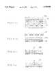
- FIG. 8is a sectional view for showing an exemplified configuration of the conventional solid state imaging device.
- a reference numeral 11denotes a semiconductor substrate
- a reference numeral 12denotes photodiodes formed on the surface of the semiconductor substrate 11 so as to convert incident light into a charge
- a reference numeral 13denotes a first flattening layer for flattening the surface of the semiconductor substrate 11
- a reference numeral 14denotes a color filter formed on the flattening layer 13
- a reference numeral 15denotes a second flattening layer for flattening the level difference on the color filter 14
- a reference numeral 50denotes micro lenses formed on the second flattening layer 15 so as to collect light on the corresponding photodiodes 12.
- the first flattening layer 13is formed by coating the semiconductor substrate 11 with a transparent film material in a desired thickness.
- the color filter 14is formed by, for example, photolithography so as to correspond to the respective photodiodes 12.
- the second flattening layer 15is formed by coating the color filter 14 with a transparent film material in a desired thickness.
- Each of the micro lenses 50is made of a phenol resin or the like, and is formed above the corresponding photodiode 12 in the shape of a hemisphere.
- the micro lens 50has an appropriate height so that light entering the surface thereof can be efficiently collected on the corresponding photodiode 12.
- the hemispherical shape of the micro lens 50is formed through the following procedures: First, a lens resin is coated on the second flattening layer 15. Then, the lens resin is subjected to an exposing treatment using a lens mask and further to a developing treatment, thereby patterning the lens resin so as to be located in the position above each of the photodiodes 12. Then, the patterned photo resist is heated so as to be melted, thereby forming the hemispherical shape of the micro lens 50 by making use of the surface tension.
- FIG. 9is a plan view of the conventional solid state imaging device taking from the upward direction, wherein a reference numeral 50 denotes micro lenses, and reference letters x and y indicate a space between the adjacent micro lenses at the center and a space therebetween at the end, respectively.
- FIG. 10is a sectional view for showing another exemplified configuration of the conventional solid state imaging device.
- a reference numeral 11denotes a semiconductor substrate
- a reference numeral 12denotes photodiodes
- a reference numeral 13denotes a first flattening layer
- a reference numeral 14denotes a color filter
- a reference numeral 15denotes a second flattening layer, all of which are similar to those shown in FIG. 8.
- This solid state imaging deviceis different from that shown in FIG. 8 in an interlayer insulating film 16 formed between the semiconductor substrate 11 and the first flattening layer 13.
- the interlayer insulating film 16has a smooth surface but has irregularity in accordance with the irregularity on the semiconductor substrate 11.
- the first flattening layer 13is formed in order to flatten the irregularity on the surface of the interlayer insulating film 16.
- the heating temperatureis set at a temperature where the lens patterns are completely melted. Therefore, the melted lens patterns are forced out of the bottoms of the intended patterns.
- the space x at the center between the adjacent micro lenses 50is smaller than the space y at the end.
- the space y at the endcannot be extremely minimized. In this manner, there is a limit in enlarging the light receiving area of each micro lens 50.
- the lens patternsare completely melted in the conventional methods, it is impossible, due to the surface tension, to make the height H of the micro lens 50 larger than a half R of the bottom width of the micro lens 50 in the alignment direction of the light receiving portions. Accordingly, when a distance between the micro lens 50 and the photodiode 12 is small, it is feared that the micro lens 50 cannot be formed into an optimal shape for collecting the light.
- the interlayer insulating film 16is formed on the semiconductor substrate 11 as in the solid state imaging device of FIG. 10, a distance between the micro lens 50 and the photodiode 12 is enlarged by the thickness of the interlayer insulating film 16. Therefore, even when the micro lens 50 has an optimal shape, there is the possibility of incident light not being collected on the photodiode 12 owing to the effects of scattering and the like. In particular when the refractive index of the interlayer insulating film 16 is larger than those of the first flattening layer 13 and the color filter 14, such a phenomenon becomes conspicuous, resulting in degrading the photosensitivity of the device.
- One object of this inventionis providing a solid state imaging device having higher photosensitivity than a conventional device. Another object of the invention is attaining high photosensitivity by suppressing the decrease thereof even in a solid state imaging device comprising an interlayer insulating film formed on a semiconductor substrate.
- a heating temperature in the formation of micro lenses in this inventionis set at a temperature lower than a temperature at which a lens resin is completely melted.
- the lens resinis coated in a large thickness, and the heating temperature in the formation of the micro lenses is set at a temperature lower than a temperature at which the lens resin is completely melted.
- each the formed micro lenseshas a larger dimension in the longitudinal direction.
- a flattening layeron an interlayer insulating film out of a material having a larger refractive index than that of the interlayer insulating film, a pseudo-convex lens for collecting light on the light receiving portion can be formed. Moreover, a material which is melted into a liquid state through a heat treatment is used for the flattening layer and a heat treatment is conducted in one of the production procedures for the device. As a result, the flattening layer can be formed in a very small thickness, so that the distance between the micro lens and the light receiving portion can be made small.
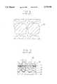
- FIGS. 1(a) through 1(d)are diagrams for showing the production procedures for micro lenses in a production method for a solid state imaging device according to a first embodiment of the invention, wherein FIGS. 1(a) through 1(d) are sectional views of the solid state imaging device in the respective procedures;
- FIG. 2is a plan view taking from the upward direction of the solid state imaging device produced by the production method of the first embodiment
- FIGS. 3(a) through 3(d)are diagrams for showing the production procedures for micro lenses in a production method for a solid state imaging device according to a second embodiment of the invention, wherein FIGS. 3(a) through 3(d) are sectional views of the solid state imaging device in the respective procedures;
- FIG. 4is a sectional view for showing the configuration of the solid state device produced by the production method of the second embodiment
- FIG. 5is a sectional view for showing the configuration of a solid state imaging device according to a third embodiment of the invention.
- FIG. 6is a sectional view for showing the configuration of a solid state imaging device according to a fourth embodiment of the invention.
- FIGS. 7(a) through 7(c)are diagrams for showing the production procedures for a flattening layer in the production method for the solid state imaging device of the fourth embodiment, wherein FIGS. 7(a) through 7(c) are sectional views of the solid state imaging device in the respective procedures;
- FIG. 8is a sectional view for showing an exemplified configuration of a conventional solid state imaging device
- FIG. 9is a plan view taking from the upward direction of the conventional solid state imaging device.
- FIG. 10is a sectional view for showing another exemplified configuration of the conventional solid state imaging device.
- FIGS. 1(a) through 1(d)show the production procedures for micro lenses in a production method for a solid state imaging device according to the first embodiment of the invention, wherein FIGS. 1(a) through 1(d) are sectional views of the solid state imaging device in the respective procedures.
- a reference numeral 11denotes a semiconductor substrate
- a reference numeral 12denotes photodiodes formed as light receiving portions on the surface of the semiconductor substrate 11 so as to convert incident light into a charge
- a reference numeral 13denotes a first flattening layer for flattening the surface of the semiconductor substrate 11
- a reference numeral 14denotes a color filter formed by, for example, the photolithography on the first flattening layer 13
- a reference numeral 15denotes a second flattening layer for flattening the level difference on the color filter 14.
- the semiconductor substrate 11, the photodiodes 12, the first flattening layer 13 and the color filter 14are omitted.
- the surface of the second flattening layer 15is coated with a lens resin 10a made of a thermoplastic resin such as phenol resins.
- the lens resin 10acan be deformed by heat and has a refractive index of 1.3 or more.
- lens masks 18are disposed above the lens resin 10a.
- the lens masks 18are arranged with pitches in accordance with the positions of the photodiodes 12.
- lens patterns 10bAs shown in FIG. 1(c). Furthermore, the lens patterns 10b are irradiated with UV in order to improve the light transmittance. In this manner, a photosensitive agent included in the lens patterns 10b is decomposed, so that the lens patterns 10b become transparent.
- the heating temperature in the heat treatmentis 130° C. through 140° C.
- the lens patterns 10bare heated to a temperature of 120° C. through 130° C.
- the lens patterns 10bstart to be melted, and when they are heated to a temperature of 150° C. through 160° C., they are completely melted.
- the heating temperaturewithin the range between 130° C. and 140° C., which is lower by 10° C. through 20° C. than the temperature at which the lens patterns are completely melted, the lens patterns 10b are prevented from being forced out of the bottoms of the intended patterns.
- each of the micro lenses 10ccan be securely formed in the shape of a hemisphere and in a sufficient height.
- a space S 2 between the adjacent micro lenses 10cis equal to a space S 1 between the adjacent lens patterns 10b. Accordingly, by bringing the space S 1 between the lens patterns 10b close to zero, the space S 2 between the micro lenses 10c can be accordingly brought close to zero, namely the surface area of each micro lens 10c can be enlarged.
- the heating temperature for the formation of the micro lenses 10cat the temperature at which the lens patterns 10b are not completely melted, it is possible to form the micro lenses 10c which can efficiently collect incident light on the corresponding photodiodes 12. Furthermore, by controlling the heating temperature within the range between 130° C. and 140° C., the shape of each micro lens 10c can be controlled.
- FIG. 2is a plan view taking from the upward direction of the solid state imaging device produced by the production method shown in FIG. 1.
- a reference numeral 10denotes micro lenses
- reference letters x and yindicate a space between the adjacent micro lenses 10 at the center and a space therebetween at the end, respectively.
- the lens patterns 10bare not completely melted, and hence, the space x at the center is equal to the space y at the end. Therefore, since both the space x at the center and the space y at the end can be minimized, the light receiving area of each micro lens 10 can be enlarged as compared with that in the conventional device.
- FIGS. 3(a) through 3(d)show the production procedures for micro lenses in a production method for a solid state imaging device according to the second embodiment of the invention, wherein the FIGS. 3(a) through 3(d) are sectional views of the solid state imaging device in the respective procedures.
- a reference numeral 11denotes a semiconductor substrate
- a reference numeral 12denotes photodiodes formed as light receiving portions
- a reference numeral 13denotes a first flattening layer
- a reference numeral 14denotes a color filter
- a reference numeral 15denotes a second flattening layer, all of which are similar to those shown in FIG. 1(a).
- the semiconductor substrate 11, the photodiodes 12, the first flattening layer 13 and the color filter 14are omitted.
- This embodimentis different from the first embodiment in a larger thickness of a lens resin 20a.
- the surface of the second flattening layer 15is coated with the lens resin 20a made of a thermoplastic resin in a thickness of 2 through 4 ⁇ m.
- lens masks 18are disposed above the lens resin 20a.
- the lens masks 18are arranged with pitches in accordance with the positions of the photodiodes
- An exposing treatmentis conducted by using the lens masks 18 and a developing treatment is further conducted, thereby forming lens patterns 20b as shown in FIG. 3(c). Furthermore, the lens patterns 20b are irradiated with UV in order to improve the light transmittance. In this manner, photosensitive agent included in the lens patterns 20b is decomposed, so that the lens patterns 20b become transparent.
- a heat treatmentis subsequently conducted, thereby forming micro lenses 20c as shown in FIG. 3(d).
- the heating temperature in the heat treatmentwithin a range between 130° C. and 140° C., which is lower by 10° C. through 20° C. than the temperature at which the lens patterns 20b are completely melted, the lens patterns 20b are prevented from being forced out of the bottoms in the intended patterns and flowing out.
- each micro lens 20ccan be formed in the shape of a hemisphere and in a sufficient height.
- the height H of each micro lens 20cis larger than a half R of the bottom width in the alignment direction of the light receiving portions. Furthermore, it is possible to prevent the shape of the micro lens 20c from being spoiled owing to the surface tension. Accordingly, the resultant micro lens has a larger longitudinal dimension.
- FIG. 4is a sectional view for showing the configuration of the solid state imaging device produced by the production method of this embodiment.
- the reference numeral 11denotes the semiconductor substrate
- the reference numeral 12denotes the photodiodes
- the reference numeral 13denotes the first flattening layer
- the reference numeral 14denotes the color filter
- the reference numeral 15denotes the second flattening layer, all of which are identical to those shown in FIG. 3(a).
- a reference numeral 20denotes micro lenses formed on the second flattening layer 15. Furthermore, a reference letter R 1 indicates the half of the bottom width of the micro lens 20 in the alignment direction of the light receiving portions, a reference letter R 2 indicates a half of the cell width in the alignment direction of the light receiving portions, and a reference letter H indicates the height of the micro lens 20.
- the adjacent micro lenses 20are actually aligned with a space therebetween of 0.1 through 1.5 ⁇ m, so as not to come in contact with each other.
- each micro lens 20is a long semiellipse which can be indicated with a cycloid curve or a parabola, and the height H is larger than the half R 1 of the bottom width in the alignment direction of the light receiving portions. Furthermore, in this embodiment, the height H of the micro lens 20 can be made larger than the half R 2 of the cell width in the alignment direction of the light receiving portions.
- FIG. 5is a sectional view for showing the configuration of a solid state imaging device of the third embodiment of the invention.
- a reference numeral 11denotes a semiconductor substrate
- a reference numeral 12denotes photodiodes formed on the surface of the semiconductor substrate as light receiving portions
- a reference numeral 16denotes an interlayer insulating film formed on the semiconductor substrate 11 as an insulating film
- a reference numeral 30denotes a first flattening layer for flattening irregularity on the surface of the interlayer insulating film 16
- a reference numeral 14denotes a color filter formed on the first flattening layer
- a reference numeral 15denotes a second flattening layer for flattening the level difference on the surface of the color filter 14
- a reference numeral 50denotes micro lenses formed on the second flattening layer 15.
- the first flattening layer 30is made of a material having a larger refractive index than that of the interlayer insulating film 16.
- the interlayer insulating film 16 and the first flattening layer 30are formed out of any of the following combinations: a silicon oxide film and a phenol resin film; a fluorine resin film and a silicon oxide film; a fluorine resin film and an acrylic resin film; a fluorine resin film and a phenol resin film; a fluorine resin film and a polyimide resin film; a silicon oxide film and an acrylic resin film; a silicon oxide film and a polyimide resin film; and an acrylic resin film and a phenol resin film.
- the interlayer insulating film 16has a thickness of approximately 0.1 through 1.5 ⁇ m.
- the first flattening layer 30 formed on the interlayer insulating film 16has a larger refractive index than those of the interlayer insulating film 16, the color filter 14 and the second flattening layer 15.
- the first flattening layer 30is made of the material having a larger refractive index than that of the interlayer insulating film 16, a pseudo-convex lens 31 facing downward is formed at each recessed portion of the interlayer insulating film 16.
- the center of the pseudo-convex lens 31accords with the center of the corresponding photodiode 12. Owing to this pseudo-convex lens 31, light which cannot be collected on the photodiode 12 in the conventional solid state imaging device can be collected on the photodiode 12 in the present device. Even through the pseudo-convex lens 31 is thus formed, the distance between the micro lens 50 and the corresponding photodiode 12 is not changed, and hence, the micro lens 50 can attain the light collecting effect to the same extent as in the conventional device.
- the curvature and the depth of the pseudo-convex lens 31can be varied by changing the thickness of the interlayer insulating film 16.
- the resultant solid state imaging devicecan achieve high photosensitivity regardless of the shape of each photodiode 12.
- the combination of this embodiment with the first or second embodimentcan further increase the photosensitivity of the solid state imaging device.
- this embodimentis applicable not only to a color solid state imaging device including a color filter but also to a black-and-white solid state imaging device including no color filter.
- FIG. 6is a sectional view for showing the configuration of a solid state imaging device of the fourth embodiment of the invention.
- a reference numeral 11denotes a semiconductor substrate
- a reference numeral 12denotes a photodiodes formed on the surface of the semiconductor substrate as a light receiving portions
- a reference numeral 16denotes an interlayer insulating film formed on the semiconductor substrate 11 as an insulating film
- a reference numeral 32denotes a first flattening layer for flattening irregularity on the surface of the interlayer insulating film 16
- a reference numeral 14denotes a color filter formed on the first flattening layer 32
- a reference numeral 15denotes a second flattening layer for flattening the level difference on the surface of the color filter 14
- a reference numeral 50denotes micro lenses formed on the second flattening layer 15.
- the interlayer insulating film 16is made of a fluorine resin film, a silicon oxide film or an acrylic resin film, and has a thickness of approximately 0.1 through 1.5 ⁇ m.
- the first flattening layer 32 formed on the interlayer insulating film 16is made of a thermoplastic resin such as phenol resins, and has a larger refractive index than those of the interlayer insulating film 16, the color filter 14 and the second flattening layer 15.
- the first flattening layer 32is made of the material having a larger refractive index than that of the interlayer insulating film 16, a pseudo-convex lens 33 facing downward is formed in each recessed portion of the interlayer insulating film 16.
- the center of the pseudo-convex lens 33accords with the center of the corresponding photodiode 12. Owing to this pseudo-convex lens 33, light which cannot be collected on the photodiode in the conventional solid state imaging device can be collected on the photodiode 12 in the present solid state imaging device.
- the first flattening layer 32has thermoplasticity, the first flattening layer 32 can be melted into a liquid state when heated, so as to provide a very thin and completely flat film. As a result, the distance between the micro lens 50 and the corresponding photodiode 12 can be minimized. Thus, the distance between the micro lens 50 and the corresponding photodiode 12 can be optimized, thereby collecting more light on the photodiode.
- the curvature and the depth of the pseudo-convex lens 33can be varied by changing the thickness of the interlayer insulating film 16.
- the resultant solid state imaging devicecan attain high photosensitivity regardless of the shape of each photodiode 12.
- FIGS. 7(a) through 7(c)are diagrams for showing the production procedures for the first flattening layer in the production method for the solid state imaging device of this embodiment, wherein FIGS. 7(a) through 7(c) are sectional views of the solid state imaging device in the respective procedures.
- the interlayer insulating film 16is formed on the semiconductor substrate 11 bearing the photodiodes 12 on its surface.
- the interlayer insulating film 16is coated with a first flattening resist 32a of a thermoplastic resin such as phenol resins. At this point, merely the coating process does not provide the first flattening resist 32a with a flat surface. Then, as is shown in FIG. 7(c), the first flattening resist 32a is heated to be melted into a liquid state, thereby forming a first flattening layer 32b. Through this heating process, the first flattening layer 32b having a flat surface and a small thickness can be obtained.
- a thermoplastic resinsuch as phenol resins
- the combination of this embodiment with the first or second embodimentcan further improve the photosensitivity of the solid state imaging device.
- this embodimentis applicable not only to a color solid state imaging device including a color filter but also to a black-and-white solid state imaging device including no color filter.
Landscapes
- Solid State Image Pick-Up Elements (AREA)
Abstract
Description
Claims (4)
Priority Applications (1)
| Application Number | Priority Date | Filing Date | Title |
|---|---|---|---|
| US09/005,048US5976907A (en) | 1995-05-02 | 1998-01-09 | Solid state imaging device and production method for the same |
Applications Claiming Priority (2)
| Application Number | Priority Date | Filing Date | Title |
|---|---|---|---|
| JP10839095 | 1995-05-02 | ||
| JP7-108390 | 1995-05-02 |
Related Child Applications (1)
| Application Number | Title | Priority Date | Filing Date |
|---|---|---|---|
| US09/005,048DivisionUS5976907A (en) | 1995-05-02 | 1998-01-09 | Solid state imaging device and production method for the same |
Publications (1)
| Publication Number | Publication Date |
|---|---|
| US5739548Atrue US5739548A (en) | 1998-04-14 |
Family
ID=14483556
Family Applications (2)
| Application Number | Title | Priority Date | Filing Date |
|---|---|---|---|
| US08/640,050Expired - LifetimeUS5739548A (en) | 1995-05-02 | 1996-04-30 | Solid state imaging device having a flattening layer and optical lenses |
| US09/005,048Expired - LifetimeUS5976907A (en) | 1995-05-02 | 1998-01-09 | Solid state imaging device and production method for the same |
Family Applications After (1)
| Application Number | Title | Priority Date | Filing Date |
|---|---|---|---|
| US09/005,048Expired - LifetimeUS5976907A (en) | 1995-05-02 | 1998-01-09 | Solid state imaging device and production method for the same |
Country Status (3)
| Country | Link |
|---|---|
| US (2) | US5739548A (en) |
| EP (1) | EP0741418A3 (en) |
| CN (1) | CN1159607A (en) |
Cited By (26)
| Publication number | Priority date | Publication date | Assignee | Title |
|---|---|---|---|---|
| US5844290A (en)* | 1996-06-27 | 1998-12-01 | Nec Corporation | Solid state image pick-up device and method for manufacturing the same |
| US5844289A (en)* | 1996-05-21 | 1998-12-01 | Nec Corporation | Solid-state image sensor with microlens and optical fiber bundle |
| US5886760A (en)* | 1996-01-10 | 1999-03-23 | Sumitomo Chemical Company, Limited | Microlens-array, production method thereof, and liquid crystal display device using the same |
| US5970317A (en)* | 1997-05-27 | 1999-10-19 | Sony Corporation | Method of forming a filter for a solid-state image sensing device |
| US6078372A (en)* | 1995-12-22 | 2000-06-20 | Samsung Electronics Co., Ltd. | LCD devices having means for dispersing light through color filters |
| US6137555A (en)* | 1997-03-26 | 2000-10-24 | Matsushita Electronics Corporation | Liquid crystal panel with uniform adhesive layer and method of manufacturing |
| US6188094B1 (en)* | 1998-03-19 | 2001-02-13 | Canon Kabushiki Kaisha | Solid-state image pickup device |
| US6218692B1 (en)* | 1999-11-23 | 2001-04-17 | Eastman Kodak Company | Color active pixel sensor with electronic shuttering, anti-blooming and low cross talk |
| US6255640B1 (en)* | 1998-03-27 | 2001-07-03 | Sony Corporation | Solid-state image sensing device and method for manufacturing solid-state image sensing device |
| US6271900B1 (en)* | 1998-03-31 | 2001-08-07 | Intel Corporation | Integrated microlens and color filter structure |
| US6452154B1 (en)* | 1999-06-03 | 2002-09-17 | Intel Corporation | Microlens for surface mount products |
| US6459131B1 (en)* | 2000-10-04 | 2002-10-01 | Hyundai Electronics Industries Co., Ltd. | CMOS image sensor and method for fabricating the same |
| US6582988B1 (en) | 1999-09-30 | 2003-06-24 | Taiwan Semiconductor Manufacturing Company | Method for forming micro lens structures |
| US20030173599A1 (en)* | 2002-01-31 | 2003-09-18 | Junichi Nakai | Semiconductor device and fabrication method therefor |
| US20040012707A1 (en)* | 1997-09-29 | 2004-01-22 | Takashi Fukusho | Solid-state image pickup device |
| US20040036823A1 (en)* | 1998-12-10 | 2004-02-26 | Takao Nishikawa | Optical substrate and display device using the same |
| US20040183086A1 (en)* | 2003-02-19 | 2004-09-23 | Junichi Nakai | Semiconductor apparatus and method for fabricating the same |
| US20050116271A1 (en)* | 2003-12-02 | 2005-06-02 | Yoshiaki Kato | Solid-state imaging device and manufacturing method thereof |
| US20060033008A1 (en)* | 2004-08-13 | 2006-02-16 | Stmicroelectronics, S.A. | Image sensor |
| US20060145055A1 (en)* | 2004-12-30 | 2006-07-06 | Kim Sang S | Image sensor and method for fabricationg the same |
| US7102676B1 (en)* | 1998-10-28 | 2006-09-05 | Canon Kabushiki Kaisha | Image pick-up apparatus and image pick-up system, and method for manufacturing image pick-up apparatus |
| US20060197097A1 (en)* | 2005-03-01 | 2006-09-07 | Canon Kabushiki Kaisha | Image pickup device with color filter |
| US20090206430A1 (en)* | 2005-08-19 | 2009-08-20 | Toshihiro Higuchi | Solid-state imaging device and method for manufacturing the same |
| US20090297991A1 (en)* | 2008-06-02 | 2009-12-03 | Fujifilm Corporation | Method for manufacturing lenticular sheet |
| US20110233704A1 (en)* | 2004-10-08 | 2011-09-29 | Kenji Yokozawa | Solid-state imaging device and solid-state imaging device manufacturing method |
| US20180240829A1 (en)* | 2015-09-07 | 2018-08-23 | Sony Semiconductor Solutions Corporation | Solid-state imaging element, manufacturing method, and electronic device |
Families Citing this family (19)
| Publication number | Priority date | Publication date | Assignee | Title |
|---|---|---|---|---|
| US6083429A (en)* | 1998-03-31 | 2000-07-04 | Intel Corporation | Microlens formation through focal plane control of a aerial image |
| US6731726B1 (en) | 1999-04-12 | 2004-05-04 | Conexant Systems, Inc. | Communication on hold |
| US6171885B1 (en)* | 1999-10-12 | 2001-01-09 | Taiwan Semiconductor Manufacturing Company | High efficiency color filter process for semiconductor array imaging devices |
| US7129982B1 (en)* | 1999-12-30 | 2006-10-31 | Intel Corporation | Color image sensor with integrated binary optical elements |
| JP2002064193A (en)* | 2000-08-22 | 2002-02-28 | Sony Corp | Solid-state imaging device and manufacturing method |
| US6482669B1 (en)* | 2001-05-30 | 2002-11-19 | Taiwan Semiconductor Manufacturing Company | Colors only process to reduce package yield loss |
| JP2004111867A (en)* | 2002-09-20 | 2004-04-08 | Canon Inc | Solid-state imaging device |
| KR100972059B1 (en)* | 2002-12-30 | 2010-07-22 | 동부일렉트로닉스 주식회사 | Manufacturing Method of CMOS Image Sensor Improved Coating Uniformity of Micro Lens |
| CN101290942B (en)* | 2003-05-28 | 2013-03-27 | 佳能株式会社 | Photoelectric conversion device and manufacturing method thereof |
| US7115853B2 (en)* | 2003-09-23 | 2006-10-03 | Micron Technology, Inc. | Micro-lens configuration for small lens focusing in digital imaging devices |
| KR100549589B1 (en)* | 2003-09-29 | 2006-02-08 | 매그나칩 반도체 유한회사 | Image sensor and its manufacturing method |
| KR100642764B1 (en)* | 2004-09-08 | 2006-11-10 | 삼성전자주식회사 | Image device and its manufacturing method |
| US20060198008A1 (en)* | 2005-03-07 | 2006-09-07 | Micron Technology, Inc. | Formation of micro lens by using flowable oxide deposition |
| KR100610497B1 (en)* | 2005-07-25 | 2006-08-09 | 삼성전자주식회사 | Method for preventing contamination of microlenses of image sensor device and manufacturing method of image sensor device using same |
| KR100760922B1 (en)* | 2006-07-31 | 2007-09-21 | 동부일렉트로닉스 주식회사 | Micro Lens of CMOS Image Sensor Using Silicon Oxide and Its Manufacturing Method |
| KR100819706B1 (en)* | 2006-12-27 | 2008-04-04 | 동부일렉트로닉스 주식회사 | CMOS image sensor and manufacturing method |
| US8003425B2 (en)* | 2008-05-14 | 2011-08-23 | International Business Machines Corporation | Methods for forming anti-reflection structures for CMOS image sensors |
| US7759755B2 (en) | 2008-05-14 | 2010-07-20 | International Business Machines Corporation | Anti-reflection structures for CMOS image sensors |
| TWI430415B (en)* | 2009-12-01 | 2014-03-11 | Xintec Inc | Chip package and fabrication method thereof |
Citations (4)
| Publication number | Priority date | Publication date | Assignee | Title |
|---|---|---|---|---|
| US5132251A (en)* | 1990-12-31 | 1992-07-21 | Samsung Electronics Co., Ltd. | Method for manufacturing a color filter |
| US5321297A (en)* | 1990-11-16 | 1994-06-14 | Kabushiki Kaisha Toshiba | Solid state image pickup device having light conversion lens formed on a strip layer |
| US5479049A (en)* | 1993-02-01 | 1995-12-26 | Sharp Kabushiki Kaisha | Solid state image sensor provided with a transparent resin layer having water repellency and oil repellency and flattening a surface thereof |
| US5555476A (en)* | 1993-08-30 | 1996-09-10 | Toray Industries, Inc. | Microlens array sheet for a liquid crystal display, method for attaching the same and liquid crystal display equipped with the same |
Family Cites Families (6)
| Publication number | Priority date | Publication date | Assignee | Title |
|---|---|---|---|---|
| JPH03276677A (en)* | 1990-03-26 | 1991-12-06 | Nec Corp | Solid-state image sensing element |
| JP2604890B2 (en)* | 1990-07-16 | 1997-04-30 | 松下電子工業株式会社 | Method for manufacturing solid-state imaging device |
| JPH04229802A (en)* | 1990-12-27 | 1992-08-19 | Toshiba Corp | Solid image pick-up device and manufacture thereof |
| JP2566087B2 (en)* | 1992-01-27 | 1996-12-25 | 株式会社東芝 | Colored microlens array and manufacturing method thereof |
| JP3318947B2 (en)* | 1992-03-05 | 2002-08-26 | ソニー株式会社 | Method for manufacturing solid-state imaging device |
| JPH05335531A (en)* | 1992-05-27 | 1993-12-17 | Sharp Corp | Solid-state imaging device |
- 1996
- 1996-04-30USUS08/640,050patent/US5739548A/ennot_activeExpired - Lifetime
- 1996-05-02EPEP96106915Apatent/EP0741418A3/ennot_activeWithdrawn
- 1996-05-02CNCN96104498Apatent/CN1159607A/enactivePending
- 1998
- 1998-01-09USUS09/005,048patent/US5976907A/ennot_activeExpired - Lifetime
Patent Citations (4)
| Publication number | Priority date | Publication date | Assignee | Title |
|---|---|---|---|---|
| US5321297A (en)* | 1990-11-16 | 1994-06-14 | Kabushiki Kaisha Toshiba | Solid state image pickup device having light conversion lens formed on a strip layer |
| US5132251A (en)* | 1990-12-31 | 1992-07-21 | Samsung Electronics Co., Ltd. | Method for manufacturing a color filter |
| US5479049A (en)* | 1993-02-01 | 1995-12-26 | Sharp Kabushiki Kaisha | Solid state image sensor provided with a transparent resin layer having water repellency and oil repellency and flattening a surface thereof |
| US5555476A (en)* | 1993-08-30 | 1996-09-10 | Toray Industries, Inc. | Microlens array sheet for a liquid crystal display, method for attaching the same and liquid crystal display equipped with the same |
Cited By (41)
| Publication number | Priority date | Publication date | Assignee | Title |
|---|---|---|---|---|
| US6323920B1 (en)* | 1995-12-22 | 2001-11-27 | Samsung Electronics Co., Ltd. | Methods of making LCD devices having color filter |
| US6078372A (en)* | 1995-12-22 | 2000-06-20 | Samsung Electronics Co., Ltd. | LCD devices having means for dispersing light through color filters |
| US5886760A (en)* | 1996-01-10 | 1999-03-23 | Sumitomo Chemical Company, Limited | Microlens-array, production method thereof, and liquid crystal display device using the same |
| US5844289A (en)* | 1996-05-21 | 1998-12-01 | Nec Corporation | Solid-state image sensor with microlens and optical fiber bundle |
| US5844290A (en)* | 1996-06-27 | 1998-12-01 | Nec Corporation | Solid state image pick-up device and method for manufacturing the same |
| US6137555A (en)* | 1997-03-26 | 2000-10-24 | Matsushita Electronics Corporation | Liquid crystal panel with uniform adhesive layer and method of manufacturing |
| US5970317A (en)* | 1997-05-27 | 1999-10-19 | Sony Corporation | Method of forming a filter for a solid-state image sensing device |
| US7259791B2 (en)* | 1997-09-29 | 2007-08-21 | Sony Corporation | Method of making solid-state image pickup device in-layer lens with antireflection film with intermediate index of refraction |
| US20040012707A1 (en)* | 1997-09-29 | 2004-01-22 | Takashi Fukusho | Solid-state image pickup device |
| US6188094B1 (en)* | 1998-03-19 | 2001-02-13 | Canon Kabushiki Kaisha | Solid-state image pickup device |
| US6605850B1 (en) | 1998-03-19 | 2003-08-12 | Canon Kabushiki Kaisha | Solid-state image pickup device using layers having different refractive indices |
| US6255640B1 (en)* | 1998-03-27 | 2001-07-03 | Sony Corporation | Solid-state image sensing device and method for manufacturing solid-state image sensing device |
| US6271900B1 (en)* | 1998-03-31 | 2001-08-07 | Intel Corporation | Integrated microlens and color filter structure |
| US6433844B2 (en) | 1998-03-31 | 2002-08-13 | Intel Corporation | Method for creating a color microlens array of a color display layer |
| US20070075247A1 (en)* | 1998-10-28 | 2007-04-05 | Canon Kabushiki Kaisha | Image pick-up apparatus and image pick-up system, and method for manufacturing image pick-up apparatus |
| US7852392B2 (en) | 1998-10-28 | 2010-12-14 | Canon Kabushiki Kaisha | Image pick-up apparatus and image pick-up system, and method for manufacturing image pick-up apparatus |
| US7102676B1 (en)* | 1998-10-28 | 2006-09-05 | Canon Kabushiki Kaisha | Image pick-up apparatus and image pick-up system, and method for manufacturing image pick-up apparatus |
| US20040036823A1 (en)* | 1998-12-10 | 2004-02-26 | Takao Nishikawa | Optical substrate and display device using the same |
| US7042644B2 (en)* | 1998-12-10 | 2006-05-09 | Seiko Epson Corporation | Optical substrate and display device using the same |
| US6452154B1 (en)* | 1999-06-03 | 2002-09-17 | Intel Corporation | Microlens for surface mount products |
| US6582988B1 (en) | 1999-09-30 | 2003-06-24 | Taiwan Semiconductor Manufacturing Company | Method for forming micro lens structures |
| US6218692B1 (en)* | 1999-11-23 | 2001-04-17 | Eastman Kodak Company | Color active pixel sensor with electronic shuttering, anti-blooming and low cross talk |
| US6459131B1 (en)* | 2000-10-04 | 2002-10-01 | Hyundai Electronics Industries Co., Ltd. | CMOS image sensor and method for fabricating the same |
| US20030173599A1 (en)* | 2002-01-31 | 2003-09-18 | Junichi Nakai | Semiconductor device and fabrication method therefor |
| US6753557B2 (en)* | 2002-01-31 | 2004-06-22 | Sharp Kabushiki Kaisha | Semiconductor device having a condenser lens for use in light receiving device or light emitting device |
| US20040183086A1 (en)* | 2003-02-19 | 2004-09-23 | Junichi Nakai | Semiconductor apparatus and method for fabricating the same |
| US7453130B2 (en)* | 2003-02-19 | 2008-11-18 | Sharp Kabushiki Kaisha | Semiconductor apparatus and method for fabricating the same |
| US20050116271A1 (en)* | 2003-12-02 | 2005-06-02 | Yoshiaki Kato | Solid-state imaging device and manufacturing method thereof |
| US7291826B2 (en)* | 2004-08-13 | 2007-11-06 | Stmicroelectronics S.A. | Image sensor with a conjugate lens arrangement |
| US20060033008A1 (en)* | 2004-08-13 | 2006-02-16 | Stmicroelectronics, S.A. | Image sensor |
| US20110233704A1 (en)* | 2004-10-08 | 2011-09-29 | Kenji Yokozawa | Solid-state imaging device and solid-state imaging device manufacturing method |
| US8134110B2 (en) | 2004-10-08 | 2012-03-13 | Panasonic Corporation | Solid-state imaging device and solid-state imaging device manufacturing method |
| US7414232B2 (en)* | 2004-12-30 | 2008-08-19 | Dongbu Electronics Co., Ltd. | Image sensor and method for fabricating the same |
| CN100429779C (en)* | 2004-12-30 | 2008-10-29 | 东部亚南半导体株式会社 | Image sensor and manufacturing method thereof |
| US20060145055A1 (en)* | 2004-12-30 | 2006-07-06 | Kim Sang S | Image sensor and method for fabricationg the same |
| US20060197097A1 (en)* | 2005-03-01 | 2006-09-07 | Canon Kabushiki Kaisha | Image pickup device with color filter |
| US7683388B2 (en)* | 2005-03-01 | 2010-03-23 | Canon Kabushiki Kaisha | Image pickup device with color filter arranged for each color on interlayer lenses |
| US20090206430A1 (en)* | 2005-08-19 | 2009-08-20 | Toshihiro Higuchi | Solid-state imaging device and method for manufacturing the same |
| US20090297991A1 (en)* | 2008-06-02 | 2009-12-03 | Fujifilm Corporation | Method for manufacturing lenticular sheet |
| US20180240829A1 (en)* | 2015-09-07 | 2018-08-23 | Sony Semiconductor Solutions Corporation | Solid-state imaging element, manufacturing method, and electronic device |
| US11041980B2 (en)* | 2015-09-07 | 2021-06-22 | Sony Semiconductor Solutions Corporation | Solid-state imaging element, manufacturing method, and electronic device |
Also Published As
| Publication number | Publication date |
|---|---|
| EP0741418A2 (en) | 1996-11-06 |
| US5976907A (en) | 1999-11-02 |
| EP0741418A3 (en) | 1998-06-03 |
| CN1159607A (en) | 1997-09-17 |
Similar Documents
| Publication | Publication Date | Title |
|---|---|---|
| US5739548A (en) | Solid state imaging device having a flattening layer and optical lenses | |
| US6940654B1 (en) | Lens array and method of making same | |
| US6950140B2 (en) | Solid image-pickup device having a micro lens array and method of manufacturing the same | |
| US6524772B1 (en) | Method of manufacturing phase grating image sensor | |
| JP4527967B2 (en) | Focusing plate master and manufacturing method thereof | |
| JP4696927B2 (en) | Manufacturing method of microlens array | |
| JP3117886B2 (en) | Mask for forming resist pattern, method for forming resist pattern, and method for manufacturing lens | |
| KR100698091B1 (en) | CMOS image sensor and its manufacturing method | |
| KR101196318B1 (en) | Method for fabricating micro lens and micro lens array | |
| JP4557242B2 (en) | Photomask for controlling exposure amount and method for manufacturing the same | |
| KR20060136072A (en) | CMOS Image sensor and method for manufacturing the same | |
| JP3672663B2 (en) | Solid-state imaging device and manufacturing method thereof | |
| JP3992713B2 (en) | CMOS image sensor and manufacturing method thereof | |
| JPH06194502A (en) | Microlens and microlens array and their production | |
| US20070172974A1 (en) | Fabrication method of CMOS image sensor | |
| KR20010061586A (en) | Method for fabricating microlens in image sensor | |
| JP2001296649A (en) | Distributed density mask, method for manufacturing the same, and method for forming surface shape | |
| JP3131019B2 (en) | Optical component manufacturing method | |
| KR100672697B1 (en) | Manufacturing Method of CMOS Image Sensor | |
| JP3402479B2 (en) | Method for manufacturing solid-state imaging device | |
| JP2007035837A (en) | Solid-state imaging device and manufacturing method thereof | |
| KR20020072659A (en) | Method of fabricating a microlens | |
| JP5565771B2 (en) | Microlens manufacturing method and imaging device | |
| KR960007880B1 (en) | Making method of micro-lenses | |
| JPH0474471A (en) | How to make microlenses |
Legal Events
| Date | Code | Title | Description |
|---|---|---|---|
| AS | Assignment | Owner name:MATSUSHITA ELECTRONICS CORPORATION, JAPAN Free format text:ASSIGNMENT OF ASSIGNORS INTEREST;ASSIGNORS:SHIGETA, YOKO;ICHIKAWA, MICHIYO;TSUKAMOTO, AKIRA;REEL/FRAME:007995/0038 Effective date:19960426 | |
| STCF | Information on status: patent grant | Free format text:PATENTED CASE | |
| FEPP | Fee payment procedure | Free format text:PAYER NUMBER DE-ASSIGNED (ORIGINAL EVENT CODE: RMPN); ENTITY STATUS OF PATENT OWNER: LARGE ENTITY Free format text:PAYOR NUMBER ASSIGNED (ORIGINAL EVENT CODE: ASPN); ENTITY STATUS OF PATENT OWNER: LARGE ENTITY | |
| FPAY | Fee payment | Year of fee payment:4 | |
| AS | Assignment | Owner name:MATSUSHITA ELECTRIC INDUSTRIAL CO., LTD., JAPAN Free format text:CHANGE OF NAME;ASSIGNOR:MATSUSHITA ELECTRONICS CORPORATION;REEL/FRAME:012495/0898 Effective date:20010404 | |
| FPAY | Fee payment | Year of fee payment:8 | |
| FPAY | Fee payment | Year of fee payment:12 | |
| AS | Assignment | Owner name:PANASONIC CORPORATION, JAPAN Free format text:CHANGE OF NAME;ASSIGNOR:MATSUSHITA ELECTRIC INDUSTRIAL CO., LTD.;REEL/FRAME:031947/0358 Effective date:20081001 | |
| AS | Assignment | Owner name:PANASONIC CORPORATION, JAPAN Free format text:LIEN;ASSIGNOR:COLLABO INNOVATIONS, INC.;REEL/FRAME:031997/0445 Effective date:20131213 | |
| AS | Assignment | Owner name:COLLABO INNOVATIONS, INC., CANADA Free format text:ASSIGNMENT OF ASSIGNORS INTEREST;ASSIGNOR:PANASONIC CORPORATION;REEL/FRAME:033021/0806 Effective date:20131212 |