US5737766A - Programmable gate array configuration memory which allows sharing with user memory - Google Patents
Programmable gate array configuration memory which allows sharing with user memoryDownload PDFInfo
- Publication number
- US5737766A US5737766AUS08/599,883US59988396AUS5737766AUS 5737766 AUS5737766 AUS 5737766AUS 59988396 AUS59988396 AUS 59988396AUS 5737766 AUS5737766 AUS 5737766A
- Authority
- US
- United States
- Prior art keywords
- memory
- logic
- user
- memory cells
- logic function
- Prior art date
- Legal status (The legal status is an assumption and is not a legal conclusion. Google has not performed a legal analysis and makes no representation as to the accuracy of the status listed.)
- Expired - Fee Related
Links
- 230000006870functionEffects0.000claimsdescription36
- 238000004364calculation methodMethods0.000description12
- 230000008878couplingEffects0.000description4
- 238000010168coupling processMethods0.000description4
- 238000005859coupling reactionMethods0.000description4
- 230000001143conditioned effectEffects0.000description3
- 239000011159matrix materialSubstances0.000description2
- 230000009467reductionEffects0.000description2
- 238000003491arrayMethods0.000description1
- 230000002860competitive effectEffects0.000description1
- 239000004020conductorSubstances0.000description1
- 230000001419dependent effectEffects0.000description1
- 238000000034methodMethods0.000description1
- 230000008569processEffects0.000description1
- 239000004065semiconductorSubstances0.000description1
Images


Classifications
- H—ELECTRICITY
- H03—ELECTRONIC CIRCUITRY
- H03K—PULSE TECHNIQUE
- H03K19/00—Logic circuits, i.e. having at least two inputs acting on one output; Inverting circuits
- H03K19/02—Logic circuits, i.e. having at least two inputs acting on one output; Inverting circuits using specified components
- H03K19/173—Logic circuits, i.e. having at least two inputs acting on one output; Inverting circuits using specified components using elementary logic circuits as components
- H03K19/177—Logic circuits, i.e. having at least two inputs acting on one output; Inverting circuits using specified components using elementary logic circuits as components arranged in matrix form
- H03K19/17748—Structural details of configuration resources
- H03K19/1776—Structural details of configuration resources for memories
- H—ELECTRICITY
- H03—ELECTRONIC CIRCUITRY
- H03K—PULSE TECHNIQUE
- H03K19/00—Logic circuits, i.e. having at least two inputs acting on one output; Inverting circuits
- H03K19/02—Logic circuits, i.e. having at least two inputs acting on one output; Inverting circuits using specified components
- H03K19/173—Logic circuits, i.e. having at least two inputs acting on one output; Inverting circuits using specified components using elementary logic circuits as components
- H03K19/1733—Controllable logic circuits
- H03K19/1735—Controllable logic circuits by wiring, e.g. uncommitted logic arrays
- H03K19/1736—Controllable logic circuits by wiring, e.g. uncommitted logic arrays in which the wiring can be modified
- H—ELECTRICITY
- H03—ELECTRONIC CIRCUITRY
- H03K—PULSE TECHNIQUE
- H03K19/00—Logic circuits, i.e. having at least two inputs acting on one output; Inverting circuits
- H03K19/02—Logic circuits, i.e. having at least two inputs acting on one output; Inverting circuits using specified components
- H03K19/173—Logic circuits, i.e. having at least two inputs acting on one output; Inverting circuits using specified components using elementary logic circuits as components
- H03K19/177—Logic circuits, i.e. having at least two inputs acting on one output; Inverting circuits using specified components using elementary logic circuits as components arranged in matrix form
- H03K19/17704—Logic circuits, i.e. having at least two inputs acting on one output; Inverting circuits using specified components using elementary logic circuits as components arranged in matrix form the logic functions being realised by the interconnection of rows and columns
Definitions
- This inventionrelates generally to field programmable gate arrays (FPGAs).
- FPGAsfield programmable gate arrays
- a single array of memorycomprises both configurable memory and user memory, and in which both logic circuits of the FPGA and an external controller can access the configurable memory and the user memory.
- FPGAsare revolutionizing the way digital electronics system designers implement logic. By radically reducing the development costs and the turnaround time for implementing thousands of gates of logic, FPGAs provide new capabilities that affect the semiconductor industry. FPGAs are changing the way digital systems will be designed in the future.
- a FPGAtypically includes an array of programmable logic blocks that can be programmably interconnected to each other to provide the logic function desired by the digital electronics designer. Each of the programmable logic blocks may be individually programmed to perform any one of a number of different logic functions.
- the FPGAhas configurable routing matrices for coupling the programmable logic blocks together according to a desired configuration.
- the FPGAalso includes configuration memory cells. The configuration memory cells are coupled to the programmable logic blocks for specifying the function performed by each programmable logic block, and to the configurable routing matrices for specifying the coupling of the inputs and the outputs of the programmable logic blocks.
- Each programmable logic blockis coupled to several configuration memory cells.
- Each configuration routing matrixis coupled to several configuration memory cells. By storing different values in the configuration memory cells, each programmable logic block may be individually programmed as to its function and coupling.
- Each programmable logic block and configurable routing matrixcomprise a plurality of programmable switch elements.
- the settings of the programmable switch elementsdefine the logic function performed by each programmable logic block and the coupling of the inputs and the outputs of the programmable logic blocks.
- the settings of the programmable switch elementsare determined by the information stored within the configuration memory cells.
- each configuration memory cellcorresponds to a particular programmable switch element. To modify the setting of a programmable switch element and thereby modify the logic defined by a logic block, the information within the configuration memory cells must be modified.
- the logic which the programmable switch elements defineis generally designated as user logic.
- the user logic within a FPGArequires user memory during operation.
- User memoryis memory that the user logic has the capability to access.
- the configurable memory in which the FPGA user logic configuration is storedis not accessible as user memory.
- allowing configuration memory to be used as user memoryis too risky because of the possibility that the user might inadvertently reconfigure the FPGA causing faulty operation. Therefore, separate user memory is generally implemented.
- the implementation of separate configuration memory and user memoryleads to a duplication of resources associated with the user memory and the configuration memory.
- Duplicated resourcesinclude row and column address decoders to the memory and sense amplifiers and read/write circuits for driving the memory input and output.
- Duplication of memory resourcesrequires more power, costs and physical size than if the memory resources were not duplicated.
- Duplication of resourcesalso requires more interconnection circuitry which slows down the operation speed of the memory.
- FPGAsoperate in two basic modes.
- the first modeis a download mode in which the configurable memory is loaded with the desired FPGA user logic configuration.
- the second modeis a user mode in which no external controller access to the configurable memory is allowed.
- the configurable memoryis accessible by a controller external to the FPGA chip. External controller access is allowed so that the external controller may load the desired FPGA configuration into the configurable memory of the FPGA.
- the FPGAis not functional when the FPGA is in the download mode. That is, the FPGA is not yet serving the function of the intended use of the FPGA.
- the configurable memory of the FPGAis not accessible by an external controller. Access is not allowed because of the risk that the FPGA configuration could be overwritten leading to an undefined FPGA configuration.
- the FPGAis functional when the FPGA is in the non-program mode. That is, the FPGA is serving the function of the intended use of the FPGA.
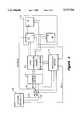
- FIG. 1A system that incorporates a FPGA 1 is shown in FIG. 1.
- An external controller 2stores information in a configuration memory 3 of the FPGA 1.
- the information stored within the configuration memoryconfigures user logic 4 of the FPGA 1.
- a separate user memory 5is required by the user logic 4 during operation. This system is redundant because two separate allocations of memory 3, 5 are supported.
- the systemrequires both configurable memory 3 and user memory 5.
- Electronic circuitryis duplicated.
- the configurable memory 3requires a column address decoder 6, a row address decoder 8 and input/output sense amplifiers with read/write circuits 10.
- the user memory 5requires a column address decoder 7, a row address decoder 9 and input/output sense amplifiers with read write circuits 11. Maintaining the configurable memory 3 and the user memory 5 requires more power and physical space than would be required if the configurable memory 3 and the user memory 5 were combined.
- the capabilities of the systemare limited because the user logic 4 cannot modify the configuration memory 3. Only the external controller 2 has the capability of modifying the configuration memory 3. Therefore, only the external controller 2 has the capability to modify the user logic 4 within the FPGA.
- the present inventiondiscloses a FPGA memory architecture that allows the same on-chip FPGA memory to be used as configurable memory and as user memory.
- the architecture of this inventionallows the user logic of the FPGA to modify information stored within the configuration memory cells. Therefore, the user logic has the capability to modify the logic that the user logic comprises. This capability allows the FPGA memory architecture of this invention to be used to solve complex problems quicker than is presently possible.
- the FPGA memory architecture of this inventionalso provides a reduction in electronic circuitry. Therefore, a reduction in cost, power and integrated circuit surface area can be realized.
- An embodiment of this inventionincludes a shared FPGA configuration memory system.
- the systemincludes a user defined logic block comprising a plurality of logic function modules, a plurality of sharable memory cells and a plurality of reconfigurable memory cells.
- Each logic function modulecomprises a plurality of programmable switch elements.
- Each reconfigurable memory cellis electrically connected to a corresponding programmable switch element. Therefore, the information stored within the reconfiguration memory cells configures logic functions within each logic function module.
- the configured logic functions within a logic function modulecan modify the reconfigurable memory cells corresponding to the programmable switch elements within the other logic function modules.
- an external controllercan also read and write information to the reconfigurable memory cells and the shareable memory cells.
- one of the logic function modulesis designated as a master logic function module which can write into the reconfigurable memory cells corresponding to the programmable switch elements within all other logic function modules. However, no other logic function module can write to the configuration memory cells corresponding to the programmable switch elements within the master logic function module.
- FIG. 1shows a prior art FPGA system that requires both FPGA configurable memory and separate user memory.
- FIG. 2shows a FPGA memory architecture according to this invention.
- FIG. 3depicts modules within the user logic in which a master module can modify the logic within servant modules.
- FIG. 4shows an implementation of the FPGA memory architecture according to this invention.
- the inventionis embodied in a FPGA memory architecture.
- the FPGA memory architecture of this inventionallows the same memory to be used as both FPGA configurable memory and as user memory.
- an external controllercan access the configuration memory and the user memory.
- the user logic defined by the configuration memorycan access the configuration memory and the user memory. Therefore, the user logic has the capability to modify the logic that the user logic comprises.
- the FPGA memory architecture of this inventionallows the user logic as defined by the information stored within the configuration memory to read from and to write to the configuration memory. By allowing the user logic to read from and write to the configuration memory, the user logic can actually modify sections of the logic within itself. The results can be disastrous if the user logic is not designed correctly. However, if designed correctly the user logic design can be very dynamic and powerful.
- the user logiccan be sectioned into modules.
- One of the modulescan be designated as the master module.
- the master moduleis configured to operated as a controller which has the capability to modify the logic within the other modules within the user logic.
- the designation of a master module that has control over the logic within the other modulesreduces the risk that the user logic will configure itself into an undefined state or configuration.
- FPGA user logicrequires user memory to properly operate. All FPGAs require configurable memory. This invention allows the user memory and the configurable memory to share memory resources such as sense amplifiers, bit lines and address decoders. Therefore, this invention also reduces cost, physical size and power consumption.
- FIG. 2shows an embodiment of this invention.
- a single array of memory 21comprises rows and columns of memory cells.
- the single array of memory 21comprises both the FPGA configurable memory and user memory.
- the configurable memory and the user memoryshare support circuitry such as data address control within an address controller 22 and data input/output control within an input/output controller 23.
- Each memory cell within the configuration memoryis electrically connected to at least one programmable switch element within a FPGA user logic block 24 through a plurality of conductors 25.
- the settings of the programmable switch elementsdetermine the logic functions within the user logic block 24. Therefore, the information stored within the configuration memory cells defines the logic functions within the user logic block 24.
- the configuration memoryis initially loaded with information by an external controller 26 while the FPGA is in the download mode. After the configuration memory has been loaded the external controller 26 switches the FPGA into the user mode. The external controller 26 must switch the FPGA back into the download mode in order for the external controller 26 to reload or modify the configuration memory.
- the user logic block 24may access the configuration memory and the user memory.
- the user logic block 24can use the user memory for storing information during a calculation and the user logic block 24 can modify the configuration memory to reconfigure a portion of the user logic block 24.
- a row of memory cells within the array of memory 21is selected by the address controller 22.
- the address controller 22is responsive to controller address inputs 27 from the external controller 26 when the FPGA is in download mode and is responsive to user address inputs 28 from the user logic block 24 when the FPGA is in the user mode.
- the input/output controller 23selects column(s) of memory within the array of memory 21 and provides a data information path.
- the input/output controller 23is responsive to the controller address inputs 27 and provides a data path from the array of memory 21 to the external controller 26 when the FPGA is in download mode.
- the input/output controller 23is responsive to the user address inputs 28 and provides a data path from the array of memory 21 to the user logic 24 when the FPGA is in user mode.
- the external controller 26determines whether the FPGA is in the download mode or the user mode. To set the FPGA into the download mode, the external controller 26 activates a mode line 29. When the mode line 29 has been activated, the address controller 22 only allows the external controller to address the array of memory 21. When the mode line 29 has been activated, the input/output controller 23 only allows the data from the array of memory to transfer between the array of memory and the external controller.
- the external controller 26deactivates the mode line 29.
- the address controller 22only allows the user logic block 24 to address the array of memory 21.
- the input/output controller 23only allows the data from the array of memory to transfer between the array of memory and the user logic block 24.
- FIG. 3depicts the user logic block 24 and modules of logic 42, 44, 46 within the user logic block 24.
- the user logic block 24 within the FPGAcan write to the configuration memory. Therefore, the user logic block 24 can modify itself if certain conditions are satisfied.
- the ability of the user logic block 24 to modify itselfis extremely risky.
- the riskis that the user logic block 24 will write into the configuration memory information that renders the user logic block 24 unusable.
- the riskcan be eliminated by sectioning the user logic block 24 into modules 42, 44, 46 and designating one of the modules 42, 44, 46 as the master module.
- FIG. 3shows module 42 as the master module and depicts the control the master module 42 has over the logic within the other modules 44, 46.
- the master modulecan be designated to control all of the writing by the user logic block 24 into the configuration memory.
- the master modulecan be configured so that the master module can write to the configuration memory cells that configure the logic of other modules 44, 46 but the configuration memory cells that correspond to the master module can not be written into. Therefore, the logic surrounding the master module within the user logic block 24 may be modified but the logic within the master module is never modified.
- This inventionmay be used to implement self repairing logic.
- FPGAscan have sections of user logic that are not fabricated properly and cannot be operated reliably.
- Self repairing logiccan be implemented which detects problem areas within the user logic.
- Self repairing logic within the user logiccan reconfigure the information stored within the configuration memory cells which correspond to the user logic to avoid the sections of user logic that were not fabricated properly. Therefore, the logic that is initially stored in the user logic checks itself for faulty operation. If any faulty operation is detected the self repairing logic within the user logic isolates where in the user logic the faulty operation resides and reconfigures the information stored within the configuration memory so that the faulty areas of the user logic are not operable.
- This inventioncan also be used to implement in hardware what is termed a self reproducing algorithm.
- a self reproducing algorithmcan be used to obtain the most efficient solution to a particular problem. For instance, a self reproducing algorithm can be used to determine the best move of a chess piece in a simulated chess game or for optimizing a circuit element within an electronic circuit.
- the determination of the best chess piece moverequires calculating how good each individual move of all the possible moves is. Therefore, a calculation must be made for every possible move. The calculation that yields the optimal result is the best move. Each best move calculation must include all of the possible future moves after the present move. The number of calculations add up very quickly and demand a great amount of computational power and memory.
- the self reproducing algorithmis implemented with this invention by initially storing a configuration within the configuration memory of the FPGA.
- the initial configurationrepresents the calculation required for the first of all of the possible chess moves.
- the user logic blockmodifies itself to a new configuration which is dependent upon the outcome of the initial calculation.
- the processrepeats.
- the user logic configurations and the calculated values for each configurationare stored within the user memory. After all of the possible configurations have been exhausted, meaning that all possible moves of the chess piece have calculated, the user memory contains all of the possible configurations and the associated results. Therefore, the best configuration corresponding to the best chess piece move can be determined.
- FIG. 4shows an implementation of the address controller 22 and the input/output controller 23 of FIGS. 2 and 3.
- the address controller 22 of FIG. 4includes a configuration row decoder 31, a user row decoder 32, a configuration row multiplexer 33 and a user row multiplexer 34.
- the configuration row multiplexer 33 and the user row multiplexer 34receive both the controller address inputs 27 and the user address inputs 28.
- the output of the configuration row multiplexer 33is connected to the input of the configuration row decoder 31.
- the output of the user row multiplexer 34is connected to the input of the user row decoder 32.
- the configuration row multiplexer 33 and the user row multiplexer 34also receive the mode line 29 from the external controller 26. When the mode line 29 is activated the configuration row multiplexer 33 and the user row multiplexer 34 pass the controller address inputs 27 through to the configuration row decoder 31 and the user row decoder 32. When the mode line 29 is deactivated the configuration row multiplexer 33 and the user row multiplexer 34 pass the user address inputs 28 through to the configuration row decoder 31 and the user row decoder 32.
- the configuration row decoder 31decodes either the controller address inputs 27 or the user address inputs 28, and determines which row of the configuration memory is to be accessed.
- the user row decoder 32decodes either the controller address inputs 27 or the user address inputs 28, and determines which row of the user memory is to be accessed.
- the input/output controller 23includes a column decoder 36, a column multiplexer 35, a column buffer 37 and a data multiplexer 38.
- the column multiplexer 35receives both the controller address inputs 27 and the user address inputs 28. The output of the column multiplexer 35 is connected to the column decoder 36. When the mode line 29 is activated the column multiplexer 35 passes the configuration address inputs 27 through to the column decoder 36. When the mode line 29 is deactivated the column multiplexer 35 passes the user address inputs 27 through to the column decoder 36.
- the column decoder 36decodes either the controller address inputs 27 or the user address inputs 28, and determines which column(s) of the user memory is to be accessed.
- Configuration or user memorygenerally includes a buffer like the column buffer 37 shown in FIG. 4.
- the buffertypically includes sense amplifiers.
- the column buffer 37is shown here to emphasize the fact that circuitry associated with the configuration memory and the user memory is minimized by combining the configuration memory and the user memory.
- the data multiplexer 38receives the mode line 29. If the mode line 29 is active, the data multiplexer 38 connects the column buffer 37 to a controller data bus 40 so that the external controller 26 can either read or write data to the array of memory 21. If the mode line 29 is not active, the data multiplexer 38 connects the column buffer 37 to a user data bus 41 so that the user logic block 24 can either read or write data to the array of memory 21.
Landscapes
- Physics & Mathematics (AREA)
- Mathematical Physics (AREA)
- Engineering & Computer Science (AREA)
- Computer Hardware Design (AREA)
- Computing Systems (AREA)
- General Engineering & Computer Science (AREA)
- Logic Circuits (AREA)
- Memory System (AREA)
- Design And Manufacture Of Integrated Circuits (AREA)
Abstract
Description
Claims (6)
Priority Applications (3)
| Application Number | Priority Date | Filing Date | Title |
|---|---|---|---|
| US08/599,883US5737766A (en) | 1996-02-14 | 1996-02-14 | Programmable gate array configuration memory which allows sharing with user memory |
| EP97300602AEP0790706A3 (en) | 1996-02-14 | 1997-01-30 | Memory system |
| JP9030203AJPH09232433A (en) | 1996-02-14 | 1997-02-14 | Programmable gate array component memory |
Applications Claiming Priority (1)
| Application Number | Priority Date | Filing Date | Title |
|---|---|---|---|
| US08/599,883US5737766A (en) | 1996-02-14 | 1996-02-14 | Programmable gate array configuration memory which allows sharing with user memory |
Publications (1)
| Publication Number | Publication Date |
|---|---|
| US5737766Atrue US5737766A (en) | 1998-04-07 |
Family
ID=24401488
Family Applications (1)
| Application Number | Title | Priority Date | Filing Date |
|---|---|---|---|
| US08/599,883Expired - Fee RelatedUS5737766A (en) | 1996-02-14 | 1996-02-14 | Programmable gate array configuration memory which allows sharing with user memory |
Country Status (3)
| Country | Link |
|---|---|
| US (1) | US5737766A (en) |
| EP (1) | EP0790706A3 (en) |
| JP (1) | JPH09232433A (en) |
Cited By (41)
| Publication number | Priority date | Publication date | Assignee | Title |
|---|---|---|---|---|
| US5940627A (en)* | 1997-03-13 | 1999-08-17 | Compaq Computer Corporation | User selectable feature set for a flash ROM based peripheral |
| US5978862A (en)* | 1997-08-08 | 1999-11-02 | Toshiba America Information Systems, Inc. | PCMCIA card dynamically configured in first mode to program FPGA controlling application specific circuit and in second mode to operate as an I/O device |
| US6078735A (en)* | 1997-09-29 | 2000-06-20 | Xilinx, Inc. | System and method for generating memory initialization logic in a target device with memory initialization bits from a programmable logic device |
| WO2001084344A1 (en)* | 2000-05-03 | 2001-11-08 | Src Computers, Inc. | Enhanced memory algorithmic processor architecture for multiprocessor computer systems |
| US6345348B2 (en)* | 1996-04-24 | 2002-02-05 | Mitsubishi Denki Kabushiki Kaisha | Memory system capable of supporting different memory devices and a memory device used therefor |
| US20020019926A1 (en)* | 1997-12-17 | 2002-02-14 | Huppenthal Jon M. | Switch/network adapter port for clustered computers employing a chain of multi-adaptive processors in a dual in-line memory module format |
| US6438737B1 (en) | 2000-02-15 | 2002-08-20 | Intel Corporation | Reconfigurable logic for a computer |
| US20030061432A1 (en)* | 1997-12-17 | 2003-03-27 | Huppenthal Jon M. | Computer system architecture and memory controller for close-coupling within a hybrid processing system utilizing an adaptive processor interface port |
| US20030097187A1 (en)* | 1997-12-17 | 2003-05-22 | Huppenthal Jon M. | Multiprocessor computer architecture incorporating a plurality of memory algorithm processors in the memory subsystem |
| KR100386253B1 (en)* | 2000-11-28 | 2003-06-02 | 엘지전자 주식회사 | Write data conviction circuit for fpga register in using parity bit |
| US20030127800A1 (en)* | 2001-11-01 | 2003-07-10 | Tyler Kenney | Tile-based board game |
| US6611466B2 (en)* | 2001-07-02 | 2003-08-26 | Samsung Electronics Co., Ltd. | Semiconductor memory device capable of adjusting the number of banks and method for adjusting the number of banks |
| US20030212853A1 (en)* | 2002-05-09 | 2003-11-13 | Huppenthal Jon M. | Adaptive processor architecture incorporating a field programmable gate array control element having at least one embedded microprocessor core |
| US20040088685A1 (en)* | 2002-10-31 | 2004-05-06 | Daniel Poznanovic | Process for converting programs in high-level programming languages to a unified executable for hybrid computing platforms |
| US20040088467A1 (en)* | 2002-10-31 | 2004-05-06 | Burton Lee A. | System and method for providing an arbitrated memory bus in a hybrid computing system |
| US20040088691A1 (en)* | 2002-10-31 | 2004-05-06 | Jeffrey Hammes | Debugging and performance profiling using control-dataflow graph representations with reconfigurable hardware emulation |
| US20040088666A1 (en)* | 2002-10-31 | 2004-05-06 | Daniel Poznanovic | System and method for partitioning control-dataflow graph representations |
| US20040088527A1 (en)* | 2002-10-31 | 2004-05-06 | Huppenthal Jon M. | Multi-adaptive processing systems and techniques for enhancing parallelism and performance of computational functions |
| US20040153752A1 (en)* | 2002-12-02 | 2004-08-05 | Marvell International Ltd. | Self-reparable semiconductor and method thereof |
| US20040161162A1 (en)* | 2002-10-31 | 2004-08-19 | Jeffrey Hammes | Efficiency of reconfigurable hardware |
| US20050015660A1 (en)* | 2002-12-02 | 2005-01-20 | Marvell World Trade Ltd. | Self-reparable semiconductor and method thereof |
| US20060001669A1 (en)* | 2002-12-02 | 2006-01-05 | Sehat Sutardja | Self-reparable semiconductor and method thereof |
| US20060012395A1 (en)* | 2002-05-09 | 2006-01-19 | Huppenthal Jon M | Reconfigurable processor element utilizing both course and fine grained reconfigurable elements |
| US20070088886A1 (en)* | 2005-10-17 | 2007-04-19 | Src Computers, Inc. | Dynamic priority conflict resolution in a multi-processor computer system having shared resources |
| US20070182600A1 (en)* | 1998-03-16 | 2007-08-09 | Actel Corporation | Sram bus architecture and interconnect to an fpga |
| US20070192241A1 (en)* | 2005-12-02 | 2007-08-16 | Metlapalli Kumar C | Methods and systems for computing platform |
| US7299458B2 (en) | 2002-10-31 | 2007-11-20 | Src Computers, Inc. | System and method for converting control flow graph representations to control-dataflow graph representations |
| CN100359602C (en)* | 2002-06-20 | 2008-01-02 | 中兴通讯股份有限公司 | Method for effectively utilizing memory in site programmable gate array |
| WO2007120439A3 (en)* | 2006-04-14 | 2008-03-20 | Raytheon Co | Data storing |
| US20080184004A1 (en)* | 2007-01-31 | 2008-07-31 | Tyler Thorp | Methods and apparatus for using a configuration array similar to an associated data array |
| US20080184005A1 (en)* | 2007-01-31 | 2008-07-31 | Tyler Thorp | Methods and apparatus for using a configuration array similar to an associated data array |
| US7565461B2 (en) | 1997-12-17 | 2009-07-21 | Src Computers, Inc. | Switch/network adapter port coupling a reconfigurable processing element to one or more microprocessors for use with interleaved memory controllers |
| US20100126043A1 (en)* | 2008-11-24 | 2010-05-27 | Srl, Inc. | Articles of Footwear |
| US8092307B2 (en) | 1996-11-14 | 2012-01-10 | Bally Gaming International, Inc. | Network gaming system |
| US8576865B1 (en) | 2010-06-07 | 2013-11-05 | Marvell International Ltd. | Physical layer devices for network switches |
| US20140245061A1 (en)* | 2013-02-28 | 2014-08-28 | Nec Corporation | Fault Repair Apparatus, Fault Repair Method and Storage Medium Storing Fault Repair Program |
| US20160285711A1 (en)* | 2014-11-03 | 2016-09-29 | Google Inc. | Data Flow Windowing and Triggering |
| US9830957B1 (en)* | 2014-09-03 | 2017-11-28 | Marvell International Ltd. | System and method of memory electrical repair |
| US10782759B1 (en) | 2019-04-23 | 2020-09-22 | Arbor Company, Lllp | Systems and methods for integrating batteries with stacked integrated circuit die elements |
| US10802735B1 (en)* | 2019-04-23 | 2020-10-13 | Arbor Company, Lllp | Systems and methods for reconfiguring dual-function cell arrays |
| US11463524B2 (en) | 2020-06-29 | 2022-10-04 | Arbor Company, Lllp | Mobile IoT edge device using 3D-die stacking re-configurable processor module with 5G processor-independent modem |
Families Citing this family (12)
| Publication number | Priority date | Publication date | Assignee | Title |
|---|---|---|---|---|
| US5959466A (en) | 1997-01-31 | 1999-09-28 | Actel Corporation | Field programmable gate array with mask programmed input and output buffers |
| US5821776A (en)* | 1997-01-31 | 1998-10-13 | Actel Corporation | Field programmable gate array with mask programmed analog function circuits |
| US6150837A (en) | 1997-02-28 | 2000-11-21 | Actel Corporation | Enhanced field programmable gate array |
| EP0984403A1 (en)* | 1998-09-01 | 2000-03-08 | Mindport B.V. | Security system |
| US6347346B1 (en)* | 1999-06-30 | 2002-02-12 | Chameleon Systems, Inc. | Local memory unit system with global access for use on reconfigurable chips |
| DE19946752A1 (en)* | 1999-09-29 | 2001-04-12 | Infineon Technologies Ag | Reconfigurable gate array |
| AU2001270876A1 (en)* | 2000-07-20 | 2002-02-05 | Celoxica Limited | System, method and article of manufacture for dynamic programming of one reconfigurable logic device from another reconfigurable logic device |
| AU2001270874A1 (en)* | 2000-07-20 | 2002-02-05 | Celoxica Limited | System, method and article of manufacture for controlling the use of resources |
| US20030041129A1 (en)* | 2000-07-20 | 2003-02-27 | John Applcby-Allis | Voice-over-internet protocol telephone in reconfigurable logic |
| US20020010825A1 (en)* | 2000-07-20 | 2002-01-24 | Alex Wilson | Memory resource arbitrator for multiple gate arrays |
| WO2003079549A1 (en)* | 2002-03-18 | 2003-09-25 | Koninklijke Philips Electronics N.V. | Configuration memory implementation for lut-based reconfigurable logic architectures |
| CN114341986B (en)* | 2019-04-23 | 2023-03-28 | 乔木有限责任合伙公司 | System and method for reconfiguring an array of dual function units |
Citations (6)
| Publication number | Priority date | Publication date | Assignee | Title |
|---|---|---|---|---|
| US5099150A (en)* | 1989-09-29 | 1992-03-24 | Sgs-Thomson Microelectronics, Inc. | Circuit block for programmable logic devices, configurable as a user-writable memory or a logic circuit |
| US5414377A (en)* | 1992-12-21 | 1995-05-09 | Xilinx, Inc. | Logic block with look-up table for configuration and memory |
| US5432719A (en)* | 1989-07-28 | 1995-07-11 | Xilinx, Inc. | Distributed memory architecture for a configurable logic array and method for using distribution memory |
| US5469003A (en)* | 1992-11-05 | 1995-11-21 | Xilinx, Inc. | Hierarchically connectable configurable cellular array |
| US5583450A (en)* | 1995-08-18 | 1996-12-10 | Xilinx, Inc. | Sequencer for a time multiplexed programmable logic device |
| US5600597A (en)* | 1995-05-02 | 1997-02-04 | Xilinx, Inc. | Register protection structure for FPGA |
Family Cites Families (1)
| Publication number | Priority date | Publication date | Assignee | Title |
|---|---|---|---|---|
| EP0665998A4 (en)* | 1993-08-03 | 1996-06-12 | Xilinx Inc | Microprocessor-based fpga. |
- 1996
- 1996-02-14USUS08/599,883patent/US5737766A/ennot_activeExpired - Fee Related
- 1997
- 1997-01-30EPEP97300602Apatent/EP0790706A3/ennot_activeWithdrawn
- 1997-02-14JPJP9030203Apatent/JPH09232433A/enactivePending
Patent Citations (6)
| Publication number | Priority date | Publication date | Assignee | Title |
|---|---|---|---|---|
| US5432719A (en)* | 1989-07-28 | 1995-07-11 | Xilinx, Inc. | Distributed memory architecture for a configurable logic array and method for using distribution memory |
| US5099150A (en)* | 1989-09-29 | 1992-03-24 | Sgs-Thomson Microelectronics, Inc. | Circuit block for programmable logic devices, configurable as a user-writable memory or a logic circuit |
| US5469003A (en)* | 1992-11-05 | 1995-11-21 | Xilinx, Inc. | Hierarchically connectable configurable cellular array |
| US5414377A (en)* | 1992-12-21 | 1995-05-09 | Xilinx, Inc. | Logic block with look-up table for configuration and memory |
| US5600597A (en)* | 1995-05-02 | 1997-02-04 | Xilinx, Inc. | Register protection structure for FPGA |
| US5583450A (en)* | 1995-08-18 | 1996-12-10 | Xilinx, Inc. | Sequencer for a time multiplexed programmable logic device |
Cited By (88)
| Publication number | Priority date | Publication date | Assignee | Title |
|---|---|---|---|---|
| US6345348B2 (en)* | 1996-04-24 | 2002-02-05 | Mitsubishi Denki Kabushiki Kaisha | Memory system capable of supporting different memory devices and a memory device used therefor |
| US8092307B2 (en) | 1996-11-14 | 2012-01-10 | Bally Gaming International, Inc. | Network gaming system |
| US8172683B2 (en) | 1996-11-14 | 2012-05-08 | Bally Gaming International, Inc. | Network gaming system |
| US8550921B2 (en) | 1996-11-14 | 2013-10-08 | Bally Gaming, Inc. | Network gaming system |
| US5940627A (en)* | 1997-03-13 | 1999-08-17 | Compaq Computer Corporation | User selectable feature set for a flash ROM based peripheral |
| US5978862A (en)* | 1997-08-08 | 1999-11-02 | Toshiba America Information Systems, Inc. | PCMCIA card dynamically configured in first mode to program FPGA controlling application specific circuit and in second mode to operate as an I/O device |
| US6078735A (en)* | 1997-09-29 | 2000-06-20 | Xilinx, Inc. | System and method for generating memory initialization logic in a target device with memory initialization bits from a programmable logic device |
| US20030061432A1 (en)* | 1997-12-17 | 2003-03-27 | Huppenthal Jon M. | Computer system architecture and memory controller for close-coupling within a hybrid processing system utilizing an adaptive processor interface port |
| US20030097187A1 (en)* | 1997-12-17 | 2003-05-22 | Huppenthal Jon M. | Multiprocessor computer architecture incorporating a plurality of memory algorithm processors in the memory subsystem |
| US6961841B2 (en) | 1997-12-17 | 2005-11-01 | Src Computers, Inc. | Multiprocessor computer architecture incorporating a plurality of memory algorithm processors in the memory subsystem |
| US7237091B2 (en) | 1997-12-17 | 2007-06-26 | Src Computers, Inc. | Multiprocessor computer architecture incorporating a plurality of memory algorithm processors in the memory subsystem |
| US7421524B2 (en) | 1997-12-17 | 2008-09-02 | Src Computers, Inc. | Switch/network adapter port for clustered computers employing a chain of multi-adaptive processors in a dual in-line memory module format |
| US20020019926A1 (en)* | 1997-12-17 | 2002-02-14 | Huppenthal Jon M. | Switch/network adapter port for clustered computers employing a chain of multi-adaptive processors in a dual in-line memory module format |
| US6339819B1 (en)* | 1997-12-17 | 2002-01-15 | Src Computers, Inc. | Multiprocessor with each processor element accessing operands in loaded input buffer and forwarding results to FIFO output buffer |
| US7003593B2 (en) | 1997-12-17 | 2006-02-21 | Src Computers, Inc. | Computer system architecture and memory controller for close-coupling within a hybrid processing system utilizing an adaptive processor interface port |
| US7565461B2 (en) | 1997-12-17 | 2009-07-21 | Src Computers, Inc. | Switch/network adapter port coupling a reconfigurable processing element to one or more microprocessors for use with interleaved memory controllers |
| US7444456B2 (en)* | 1998-03-16 | 2008-10-28 | Actel Corporation | SRAM bus architecture and interconnect to an FPGA |
| US20070182600A1 (en)* | 1998-03-16 | 2007-08-09 | Actel Corporation | Sram bus architecture and interconnect to an fpga |
| US6438737B1 (en) | 2000-02-15 | 2002-08-20 | Intel Corporation | Reconfigurable logic for a computer |
| AU2001245761B2 (en)* | 2000-05-03 | 2006-11-23 | Src Computers Llc | Enhanced memory algorithmic processor architecture for multiprocessor computer systems |
| WO2001084344A1 (en)* | 2000-05-03 | 2001-11-08 | Src Computers, Inc. | Enhanced memory algorithmic processor architecture for multiprocessor computer systems |
| KR100386253B1 (en)* | 2000-11-28 | 2003-06-02 | 엘지전자 주식회사 | Write data conviction circuit for fpga register in using parity bit |
| US6611466B2 (en)* | 2001-07-02 | 2003-08-26 | Samsung Electronics Co., Ltd. | Semiconductor memory device capable of adjusting the number of banks and method for adjusting the number of banks |
| US20030127800A1 (en)* | 2001-11-01 | 2003-07-10 | Tyler Kenney | Tile-based board game |
| US20030212853A1 (en)* | 2002-05-09 | 2003-11-13 | Huppenthal Jon M. | Adaptive processor architecture incorporating a field programmable gate array control element having at least one embedded microprocessor core |
| US7406573B2 (en) | 2002-05-09 | 2008-07-29 | Src Computers, Inc. | Reconfigurable processor element utilizing both coarse and fine grained reconfigurable elements |
| US20060012395A1 (en)* | 2002-05-09 | 2006-01-19 | Huppenthal Jon M | Reconfigurable processor element utilizing both course and fine grained reconfigurable elements |
| US20050257029A1 (en)* | 2002-05-09 | 2005-11-17 | Src Computers,Inc. | Adaptive processor architecture incorporating a field programmable gate array control element having at least one embedded microprocessor core |
| CN100359602C (en)* | 2002-06-20 | 2008-01-02 | 中兴通讯股份有限公司 | Method for effectively utilizing memory in site programmable gate array |
| US6941539B2 (en) | 2002-10-31 | 2005-09-06 | Src Computers, Inc. | Efficiency of reconfigurable hardware |
| US20040088527A1 (en)* | 2002-10-31 | 2004-05-06 | Huppenthal Jon M. | Multi-adaptive processing systems and techniques for enhancing parallelism and performance of computational functions |
| US20040088685A1 (en)* | 2002-10-31 | 2004-05-06 | Daniel Poznanovic | Process for converting programs in high-level programming languages to a unified executable for hybrid computing platforms |
| US20060041872A1 (en)* | 2002-10-31 | 2006-02-23 | Daniel Poznanovic | Process for converting programs in high-level programming languages to a unified executable for hybrid computing platforms |
| US7134120B2 (en) | 2002-10-31 | 2006-11-07 | Src Computers, Inc. | Map compiler pipelined loop structure |
| US6983456B2 (en) | 2002-10-31 | 2006-01-03 | Src Computers, Inc. | Process for converting programs in high-level programming languages to a unified executable for hybrid computing platforms |
| US7155708B2 (en) | 2002-10-31 | 2006-12-26 | Src Computers, Inc. | Debugging and performance profiling using control-dataflow graph representations with reconfigurable hardware emulation |
| US20040088467A1 (en)* | 2002-10-31 | 2004-05-06 | Burton Lee A. | System and method for providing an arbitrated memory bus in a hybrid computing system |
| US20040088691A1 (en)* | 2002-10-31 | 2004-05-06 | Jeffrey Hammes | Debugging and performance profiling using control-dataflow graph representations with reconfigurable hardware emulation |
| US7703085B2 (en) | 2002-10-31 | 2010-04-20 | Src Computers, Inc. | Process for converting programs in high-level programming languages to a unified executable for hybrid computing platforms |
| US7225324B2 (en) | 2002-10-31 | 2007-05-29 | Src Computers, Inc. | Multi-adaptive processing systems and techniques for enhancing parallelism and performance of computational functions |
| US6964029B2 (en) | 2002-10-31 | 2005-11-08 | Src Computers, Inc. | System and method for partitioning control-dataflow graph representations |
| US6996656B2 (en) | 2002-10-31 | 2006-02-07 | Src Computers, Inc. | System and method for providing an arbitrated memory bus in a hybrid computing system |
| US7620800B2 (en) | 2002-10-31 | 2009-11-17 | Src Computers, Inc. | Multi-adaptive processing systems and techniques for enhancing parallelism and performance of computational functions |
| US7299458B2 (en) | 2002-10-31 | 2007-11-20 | Src Computers, Inc. | System and method for converting control flow graph representations to control-dataflow graph representations |
| US20040088673A1 (en)* | 2002-10-31 | 2004-05-06 | Jeffrey Hammes | Map compiler pipelined loop structure |
| US20040161162A1 (en)* | 2002-10-31 | 2004-08-19 | Jeffrey Hammes | Efficiency of reconfigurable hardware |
| US20040088666A1 (en)* | 2002-10-31 | 2004-05-06 | Daniel Poznanovic | System and method for partitioning control-dataflow graph representations |
| US7657784B2 (en) | 2002-12-02 | 2010-02-02 | Marvell World Trade Ltd. | Self-reparable semiconductor and method thereof |
| US7340644B2 (en) | 2002-12-02 | 2008-03-04 | Marvell World Trade Ltd. | Self-reparable semiconductor and method thereof |
| US20040153752A1 (en)* | 2002-12-02 | 2004-08-05 | Marvell International Ltd. | Self-reparable semiconductor and method thereof |
| US8812905B2 (en) | 2002-12-02 | 2014-08-19 | Marvell World Trade Ltd. | Self-repairable semiconductor and method thereof |
| US20060001669A1 (en)* | 2002-12-02 | 2006-01-05 | Sehat Sutardja | Self-reparable semiconductor and method thereof |
| US20070055906A1 (en)* | 2002-12-02 | 2007-03-08 | Sehat Sutardja | Self-reparable semiconductor and method thereof |
| US20080215914A1 (en)* | 2002-12-02 | 2008-09-04 | Sehat Sutardja | Self-reparable semiconductor and method thereof |
| US7185225B2 (en)* | 2002-12-02 | 2007-02-27 | Marvell World Trade Ltd. | Self-reparable semiconductor and method thereof |
| US7313723B2 (en)* | 2002-12-02 | 2007-12-25 | Marvell World Trade Ltd. | Self-reparable semiconductor and method thereof |
| US7730349B2 (en) | 2002-12-02 | 2010-06-01 | Marvell World Trade Ltd. | Self-reparable semiconductor and method thereof |
| US20050015660A1 (en)* | 2002-12-02 | 2005-01-20 | Marvell World Trade Ltd. | Self-reparable semiconductor and method thereof |
| US7373547B2 (en)* | 2002-12-02 | 2008-05-13 | Marvell World Trade Ltd. | Self-reparable semiconductor and method thereof |
| US20070088886A1 (en)* | 2005-10-17 | 2007-04-19 | Src Computers, Inc. | Dynamic priority conflict resolution in a multi-processor computer system having shared resources |
| US7890686B2 (en) | 2005-10-17 | 2011-02-15 | Src Computers, Inc. | Dynamic priority conflict resolution in a multi-processor computer system having shared resources |
| US7716100B2 (en) | 2005-12-02 | 2010-05-11 | Kuberre Systems, Inc. | Methods and systems for computing platform |
| US20070192241A1 (en)* | 2005-12-02 | 2007-08-16 | Metlapalli Kumar C | Methods and systems for computing platform |
| WO2007120439A3 (en)* | 2006-04-14 | 2008-03-20 | Raytheon Co | Data storing |
| US8351259B2 (en) | 2007-01-31 | 2013-01-08 | Sandisk 3D Llc | Methods and apparatus for using a configuration array similar to an associated data array |
| US7843729B2 (en) | 2007-01-31 | 2010-11-30 | Sandisk 3D Llc | Methods and apparatus for using a configuration array similar to an associated data array |
| US7697329B2 (en)* | 2007-01-31 | 2010-04-13 | Sandisk 3D Llc | Methods and apparatus for using a configuration array similar to an associated data array |
| US20080184005A1 (en)* | 2007-01-31 | 2008-07-31 | Tyler Thorp | Methods and apparatus for using a configuration array similar to an associated data array |
| US20080184004A1 (en)* | 2007-01-31 | 2008-07-31 | Tyler Thorp | Methods and apparatus for using a configuration array similar to an associated data array |
| US20110075466A1 (en)* | 2007-01-31 | 2011-03-31 | Tyler Thorp | Methods and apparatus for using a configuration array similar to an associated data array |
| US20100126043A1 (en)* | 2008-11-24 | 2010-05-27 | Srl, Inc. | Articles of Footwear |
| US8576865B1 (en) | 2010-06-07 | 2013-11-05 | Marvell International Ltd. | Physical layer devices for network switches |
| US8718079B1 (en) | 2010-06-07 | 2014-05-06 | Marvell International Ltd. | Physical layer devices for network switches |
| US20140245061A1 (en)* | 2013-02-28 | 2014-08-28 | Nec Corporation | Fault Repair Apparatus, Fault Repair Method and Storage Medium Storing Fault Repair Program |
| US9405612B2 (en)* | 2013-02-28 | 2016-08-02 | Nec Corporation | Fault repair apparatus, fault repair method and storage medium storing fault repair program |
| US9830957B1 (en)* | 2014-09-03 | 2017-11-28 | Marvell International Ltd. | System and method of memory electrical repair |
| US20160285711A1 (en)* | 2014-11-03 | 2016-09-29 | Google Inc. | Data Flow Windowing and Triggering |
| US10037187B2 (en)* | 2014-11-03 | 2018-07-31 | Google Llc | Data flow windowing and triggering |
| US10732928B1 (en) | 2014-11-03 | 2020-08-04 | Google Llc | Data flow windowing and triggering |
| US10782759B1 (en) | 2019-04-23 | 2020-09-22 | Arbor Company, Lllp | Systems and methods for integrating batteries with stacked integrated circuit die elements |
| US10802735B1 (en)* | 2019-04-23 | 2020-10-13 | Arbor Company, Lllp | Systems and methods for reconfiguring dual-function cell arrays |
| US10969977B2 (en)* | 2019-04-23 | 2021-04-06 | Arbor Company, Lllp | Systems and methods for reconfiguring dual function cell arrays |
| US11061455B2 (en) | 2019-04-23 | 2021-07-13 | Arbor Company, Lllp | Systems and methods for integrating batteries with stacked integrated circuit die elements |
| US11435800B2 (en) | 2019-04-23 | 2022-09-06 | Arbor Company, Lllp | Systems and methods for reconfiguring dual-function cell arrays |
| US11797067B2 (en) | 2019-04-23 | 2023-10-24 | Arbor Company, Lllp | Systems and methods for reconfiguring dual-function cell arrays |
| US12287687B2 (en) | 2019-04-23 | 2025-04-29 | Arbor Company, Lllp | Systems and methods for integrating batteries to maintain volatile memories and protect the volatile memories from excessive temperatures |
| US11463524B2 (en) | 2020-06-29 | 2022-10-04 | Arbor Company, Lllp | Mobile IoT edge device using 3D-die stacking re-configurable processor module with 5G processor-independent modem |
| US11895191B2 (en) | 2020-06-29 | 2024-02-06 | Arbor Company, Lllp | Mobile IoT edge device using 3D-die stacking re-configurable processor module with 5G processor-independent modem |
Also Published As
| Publication number | Publication date |
|---|---|
| EP0790706A2 (en) | 1997-08-20 |
| EP0790706A3 (en) | 1999-01-07 |
| JPH09232433A (en) | 1997-09-05 |
Similar Documents
| Publication | Publication Date | Title |
|---|---|---|
| US5737766A (en) | Programmable gate array configuration memory which allows sharing with user memory | |
| US5809281A (en) | Field programmable gate array with high speed SRAM based configurable function block configurable as high performance logic or block of SRAM | |
| US7495970B1 (en) | Flexible memory architectures for programmable logic devices | |
| JP3471088B2 (en) | Improved programmable logic cell array architecture | |
| US6222382B1 (en) | Redundancy circuitry for programmable logic devices with interleaved input circuits | |
| US6105105A (en) | Data processing system using configuration select logic, an instruction store, and sequencing logic during instruction execution | |
| US5801547A (en) | Embedded memory for field programmable gate array | |
| USRE37195E1 (en) | Programmable switch for FPGA input/output signals | |
| US7550994B1 (en) | Programmable logic device with on-chip nonvolatile user memory | |
| US5371422A (en) | Programmable logic device having multiplexers and demultiplexers randomly connected to global conductors for interconnections between logic elements | |
| US6344755B1 (en) | Programmable logic device with redundant circuitry | |
| JP2703397B2 (en) | Logical array whose configuration can be changed | |
| US5717901A (en) | Variable depth and width memory device | |
| EP0450811A2 (en) | Integrated circuit | |
| US20010015933A1 (en) | Dual port programmable logic device variable depth and width memory array | |
| GB2286703A (en) | Programmable logic device with redundancy | |
| JP2006166430A (en) | Techniques for combining volatile and non-volatile programmable logic on integrated circuits. | |
| EP0385389B1 (en) | Semiconductor integrated circuit memory enabling memory write masking | |
| US7580963B2 (en) | Semiconductor device having an arithmetic unit of a reconfigurable circuit configuration in accordance with stored configuration data and a memory storing fixed value data to be supplied to the arithmetic unit, requiring no data area for storing fixed value data to be set in a configuration memory | |
| US6029236A (en) | Field programmable gate array with high speed SRAM based configurable function block configurable as high performance logic or block of SRAM | |
| US5230058A (en) | IC chip having volatile memory cells simultaneously loaded with initialization data from uniquely associated non-volatile memory cells via switching transistors | |
| US5555214A (en) | Apparatus for serial reading and writing of random access memory arrays | |
| US5732407A (en) | Configurable random access memory for programmable logic devices | |
| US6288970B1 (en) | Programmable logic device memory array circuit having combinable single-port memory arrays | |
| US5099453A (en) | Configuration memory for programmable logic device |
Legal Events
| Date | Code | Title | Description |
|---|---|---|---|
| AS | Assignment | Owner name:HEWLETT-PACKARD COMPANY, CALIFORNIA Free format text:ASSIGNMENT OF ASSIGNORS INTEREST;ASSIGNOR:TAN, CHARLES M.C.;REEL/FRAME:008028/0911 Effective date:19960214 | |
| AS | Assignment | Owner name:HEWLETT-PACKARD COMPANY, A DELAWARE CORPORATION, C Free format text:MERGER;ASSIGNOR:HEWLETT-PACKARD COMPANY, A CALIFORNIA CORPORATION;REEL/FRAME:010841/0649 Effective date:19980520 | |
| AS | Assignment | Owner name:AGILENT TECHNOLOGIES INC, CALIFORNIA Free format text:ASSIGNMENT OF ASSIGNORS INTEREST;ASSIGNOR:HEWLETT-PACKARD COMPANY;REEL/FRAME:010977/0540 Effective date:19991101 | |
| REMI | Maintenance fee reminder mailed | ||
| LAPS | Lapse for failure to pay maintenance fees | ||
| STCH | Information on status: patent discontinuation | Free format text:PATENT EXPIRED DUE TO NONPAYMENT OF MAINTENANCE FEES UNDER 37 CFR 1.362 | |
| FP | Expired due to failure to pay maintenance fee | Effective date:20020407 | |
| AS | Assignment | Owner name:AVAGO TECHNOLOGIES GENERAL IP (SINGAPORE) PTE. LTD Free format text:ASSIGNMENT OF ASSIGNORS INTEREST;ASSIGNOR:AGILENT TECHNOLOGIES, INC.;REEL/FRAME:017675/0001 Effective date:20051201 |