US5736998A - Inkjet cartridge design for facilitating the adhesive sealing of a printhead to an ink reservoir - Google Patents
Inkjet cartridge design for facilitating the adhesive sealing of a printhead to an ink reservoirDownload PDFInfo
- Publication number
- US5736998A US5736998AUS08/398,849US39884995AUS5736998AUS 5736998 AUS5736998 AUS 5736998AUS 39884995 AUS39884995 AUS 39884995AUS 5736998 AUS5736998 AUS 5736998A
- Authority
- US
- United States
- Prior art keywords
- nozzle member
- substrate
- ink
- adhesive
- headland
- Prior art date
- Legal status (The legal status is an assumption and is not a legal conclusion. Google has not performed a legal analysis and makes no representation as to the accuracy of the status listed.)
- Expired - Lifetime
Links
Images


Classifications
- B—PERFORMING OPERATIONS; TRANSPORTING
- B41—PRINTING; LINING MACHINES; TYPEWRITERS; STAMPS
- B41J—TYPEWRITERS; SELECTIVE PRINTING MECHANISMS, i.e. MECHANISMS PRINTING OTHERWISE THAN FROM A FORME; CORRECTION OF TYPOGRAPHICAL ERRORS
- B41J2/00—Typewriters or selective printing mechanisms characterised by the printing or marking process for which they are designed
- B41J2/005—Typewriters or selective printing mechanisms characterised by the printing or marking process for which they are designed characterised by bringing liquid or particles selectively into contact with a printing material
- B41J2/01—Ink jet
- B41J2/135—Nozzles
- B41J2/16—Production of nozzles
- B41J2/1621—Manufacturing processes
- B41J2/1631—Manufacturing processes photolithography
- B—PERFORMING OPERATIONS; TRANSPORTING
- B41—PRINTING; LINING MACHINES; TYPEWRITERS; STAMPS
- B41J—TYPEWRITERS; SELECTIVE PRINTING MECHANISMS, i.e. MECHANISMS PRINTING OTHERWISE THAN FROM A FORME; CORRECTION OF TYPOGRAPHICAL ERRORS
- B41J2/00—Typewriters or selective printing mechanisms characterised by the printing or marking process for which they are designed
- B41J2/005—Typewriters or selective printing mechanisms characterised by the printing or marking process for which they are designed characterised by bringing liquid or particles selectively into contact with a printing material
- B41J2/01—Ink jet
- B41J2/135—Nozzles
- B41J2/14—Structure thereof only for on-demand ink jet heads
- B41J2/14016—Structure of bubble jet print heads
- B41J2/14024—Assembling head parts
- B—PERFORMING OPERATIONS; TRANSPORTING
- B41—PRINTING; LINING MACHINES; TYPEWRITERS; STAMPS
- B41J—TYPEWRITERS; SELECTIVE PRINTING MECHANISMS, i.e. MECHANISMS PRINTING OTHERWISE THAN FROM A FORME; CORRECTION OF TYPOGRAPHICAL ERRORS
- B41J2/00—Typewriters or selective printing mechanisms characterised by the printing or marking process for which they are designed
- B41J2/005—Typewriters or selective printing mechanisms characterised by the printing or marking process for which they are designed characterised by bringing liquid or particles selectively into contact with a printing material
- B41J2/01—Ink jet
- B41J2/135—Nozzles
- B41J2/16—Production of nozzles
- B41J2/1601—Production of bubble jet print heads
- B41J2/1603—Production of bubble jet print heads of the front shooter type
- B—PERFORMING OPERATIONS; TRANSPORTING
- B41—PRINTING; LINING MACHINES; TYPEWRITERS; STAMPS
- B41J—TYPEWRITERS; SELECTIVE PRINTING MECHANISMS, i.e. MECHANISMS PRINTING OTHERWISE THAN FROM A FORME; CORRECTION OF TYPOGRAPHICAL ERRORS
- B41J2/00—Typewriters or selective printing mechanisms characterised by the printing or marking process for which they are designed
- B41J2/005—Typewriters or selective printing mechanisms characterised by the printing or marking process for which they are designed characterised by bringing liquid or particles selectively into contact with a printing material
- B41J2/01—Ink jet
- B41J2/135—Nozzles
- B41J2/16—Production of nozzles
- B41J2/1621—Manufacturing processes
- B41J2/1623—Manufacturing processes bonding and adhesion
- B—PERFORMING OPERATIONS; TRANSPORTING
- B41—PRINTING; LINING MACHINES; TYPEWRITERS; STAMPS
- B41J—TYPEWRITERS; SELECTIVE PRINTING MECHANISMS, i.e. MECHANISMS PRINTING OTHERWISE THAN FROM A FORME; CORRECTION OF TYPOGRAPHICAL ERRORS
- B41J2/00—Typewriters or selective printing mechanisms characterised by the printing or marking process for which they are designed
- B41J2/005—Typewriters or selective printing mechanisms characterised by the printing or marking process for which they are designed characterised by bringing liquid or particles selectively into contact with a printing material
- B41J2/01—Ink jet
- B41J2/135—Nozzles
- B41J2/16—Production of nozzles
- B41J2/1621—Manufacturing processes
- B41J2/1625—Manufacturing processes electroforming
- B—PERFORMING OPERATIONS; TRANSPORTING
- B41—PRINTING; LINING MACHINES; TYPEWRITERS; STAMPS
- B41J—TYPEWRITERS; SELECTIVE PRINTING MECHANISMS, i.e. MECHANISMS PRINTING OTHERWISE THAN FROM A FORME; CORRECTION OF TYPOGRAPHICAL ERRORS
- B41J2/00—Typewriters or selective printing mechanisms characterised by the printing or marking process for which they are designed
- B41J2/005—Typewriters or selective printing mechanisms characterised by the printing or marking process for which they are designed characterised by bringing liquid or particles selectively into contact with a printing material
- B41J2/01—Ink jet
- B41J2/135—Nozzles
- B41J2/16—Production of nozzles
- B41J2/1621—Manufacturing processes
- B41J2/1626—Manufacturing processes etching
- B41J2/1628—Manufacturing processes etching dry etching
- B—PERFORMING OPERATIONS; TRANSPORTING
- B41—PRINTING; LINING MACHINES; TYPEWRITERS; STAMPS
- B41J—TYPEWRITERS; SELECTIVE PRINTING MECHANISMS, i.e. MECHANISMS PRINTING OTHERWISE THAN FROM A FORME; CORRECTION OF TYPOGRAPHICAL ERRORS
- B41J2/00—Typewriters or selective printing mechanisms characterised by the printing or marking process for which they are designed
- B41J2/005—Typewriters or selective printing mechanisms characterised by the printing or marking process for which they are designed characterised by bringing liquid or particles selectively into contact with a printing material
- B41J2/01—Ink jet
- B41J2/135—Nozzles
- B41J2/16—Production of nozzles
- B41J2/1621—Manufacturing processes
- B41J2/1632—Manufacturing processes machining
- B41J2/1634—Manufacturing processes machining laser machining
- B—PERFORMING OPERATIONS; TRANSPORTING
- B41—PRINTING; LINING MACHINES; TYPEWRITERS; STAMPS
- B41J—TYPEWRITERS; SELECTIVE PRINTING MECHANISMS, i.e. MECHANISMS PRINTING OTHERWISE THAN FROM A FORME; CORRECTION OF TYPOGRAPHICAL ERRORS
- B41J2/00—Typewriters or selective printing mechanisms characterised by the printing or marking process for which they are designed
- B41J2/005—Typewriters or selective printing mechanisms characterised by the printing or marking process for which they are designed characterised by bringing liquid or particles selectively into contact with a printing material
- B41J2/01—Ink jet
- B41J2/135—Nozzles
- B41J2/14—Structure thereof only for on-demand ink jet heads
- B41J2002/14362—Assembling elements of heads
Definitions
- the present inventiongenerally relates to inkjet and other types of printers and, more particularly, to the printhead portion of an inkjet printer.
- Thermal inkjet print cartridgesoperate by rapidly heating a small volume of ink to cause the ink to vaporize and be ejected through one of a plurality of orifices so as to print a dot of ink on a recording medium, such as a sheet of paper.
- the orificesare arranged in one or more linear arrays in a nozzle member.
- the properly sequenced ejection of ink from each orificecauses characters or other images to be printed upon the paper as the printhead is moved relative to the paper.
- the paperis typically shifted each time the printhead has moved across the paper.
- the thermal inkjet printeris fast and quiet, as only the ink strikes the paper.
- An inkjet printheadgenerally includes: (1) ink channels to supply ink from an ink reservoir to each vaporization chamber proximate to an orifice; (2) a metal orifice plate or nozzle member in which the orifices are formed in the required pattern; and (3) a silicon substrate containing a series of thin film resistors, one resistor per vaporization chamber.
- an electrical current from an external power supplyis passed through a selected thin film resistor.
- the resistoris then heated, in turn superheating a thin layer of the adjacent ink within a vaporization chamber, causing explosive vaporization, and, consequently, causing a droplet of ink to be ejected through an associated orifice onto the paper.
- inkis fed from an ink reservoir to the various vaporization chambers through an elongated hole formed in the substrate.
- the inkthen flows to a manifold area, formed in a barrier layer between the substrate and a nozzle member, then into a plurality of ink channels, and finally into the various vaporization chambers.
- This designmay be classified as a "center” feed design, whereby ink is fed to the vaporization chambers from a central location then distributed outward into the vaporization chambers.
- a sealis formed, circumscribing the hole in the substrate, between the substrate itself and the ink reservoir body.
- this ink sealis accomplished by dispensing an adhesive bead around a fluid channel in the ink reservoir body, and positioning the substrate on the adhesive bead so that the adhesive bead circumscribes the hole formed in the substrate.
- the adhesiveis then cured with a controlled blast of hot air, whereby the hot air heats up the substrate and adhesive, thereby curing the adhesive.
- This methodrequires quite a bit of time and thermal energy, since the heat must pass through a relatively thick substrate before heating up the adhesive. Further, because the seal line is under the substrate, it tends to be difficult to diagnose the cause of any ink leakage.
- the substratebe made narrower, but the length of the edge feed substrate can be shorter, for the same number of nozzles, than the center feed substrate due to the substrate structure now being less prone to cracking or breaking without the central ink feed hole.
- This shortening of the substrateenables a shorter headland and, hence, a shorter print cartridge snout. This is important when the print cartridge is installed in a printer because with a shorter print cartridge snout, the star wheels can be located closer to the pinch rollers to ensure better paper/roller contact along the transport path of the print cartridge snout.
- a barrier layerwhich may be a separate layer or formed in the nozzle member itself, includes vaporization chambers, surrounding each orifice, and ink flow channels which provide fluid communication between a ink reservoir and the vaporization chambers.
- the orificesmay be formed aligned with the conductive traces on the nozzle member so that alignment of electrodes on a substrate with respect to ends of the conductive traces also aligns the heating elements with the orifices.
- This integrated nozzle and tab circuit designis superior to the orifice plates for inkjet printheads formed of nickel and fabricated by lithographic electroforming processes as described in U.S. Pat. No.
- a nozzle member containing an array of orificeshas a substrate, having heater elements formed thereon, affixed to a back surface of the nozzle member. Each orifice in the nozzle member is associated with a single heating element formed on the substrate. The back surface of the nozzle member extends beyond the outer edges of the substrate. Ink is supplied from an ink reservoir to the orifices by a fluid channel within a barrier layer between the nozzle member and the substrate.
- the fluid channel in the barrier layermay receive ink flowing around two or more outer edges of the substrate ("edge feed”) or, in another embodiment, may receive ink which flows through a hole in the center of the substrate (“center feed”).
- the nozzle memberis adhesively sealed with respect to the ink reservoir body by forming an ink seal, circumscribing the substrate, between the back surface of the nozzle member and the body.
- This method and structure of providing a seal directly between a nozzle member and an ink reservoir bodyhas many advantages over prior art methods of providing a seal between the back surface of the substrate and the ink reservoir body.
- One advantageis that such a seal makes an edge ink-feed design possible.
- Another advantageis that, in an embodiment where the nozzle member has conductive traces formed on its bottom surface for contact to electrodes on the substrate, the adhesive seal acts to encapsulate and protect the traces near the substrate which may come in contact with ink. Additionally, since the sealant is also an adhesive, the nozzle member is directly secured to the ink reservoir body, thus forming a stronger bond between the printhead and the inkjet print cartridge.
- sealant lineis more readily observable.
- Another advantageis that it takes less time to cure the adhesive seal, since only a thin nozzle member is between the sealant and the heat source used for curing the sealant.
- a nozzle member containing an array of orificeshas a substrate, having heater elements formed thereon, affixed to a back surface of the nozzle member. Each orifice in the nozzle member is associated with a single heating element formed on the substrate. The back surface of the nozzle member extends beyond the outer edges of the substrate. Ink is supplied from an ink reservoir to the orifices by a fluid channel within a barrier layer between the nozzle member and the substrate.
- the fluid channel in the barrier layermay receive ink flowing around two or more outer edges of the substrate or, in another embodiment, may receive ink which flows through a hole in the center of the substrate.
- the nozzle memberis adhesively sealed with respect to the ink reservoir body by forming an ink seal, circumscribing the substrate, between the back surface of the nozzle member and the headland of the print cartridge body.
- This method and structure for a print cartridge headland for providing a seal directly between a nozzle member and an ink reservoir bodyhas many advantages over prior methods of providing a seal between a printhead and the ink reservoir body.
- One advantageis that such a structure reduces the occurrence of clogged nozzles during the adhesive sealing process.
- Another advantageis that there is a reduced occurrence of adhesive voids where the adhesive seal acts to encapsulate and protect the traces near the substrate which may come in contact with ink.
- a further advantageis that it is easier to control adhesive flow and bulges due to varying amounts and placement of adhesive. The above advantages provide reduced yield losses, and thus lower manufacturing costs, when manufacturing inkjet print cartridges.
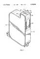
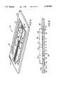
- FIG. 1is a perspective view of an inkjet print cartridge according to one embodiment of the present invention.
- FIG. 2is a perspective view of the front surface of the Tape Automated Bonding (TAB) printhead assembly (hereinafter “TAB head assembly”) removed from the print cartridge of FIG. 1.
- TAB head assemblyTape Automated Bonding
- FIG. 3is a perspective view of an simplified schematic of the inkjet print cartridge of FIG. 1. for illustrative purposes.
- FIG. 4is a perspective view of the front surface of the Tape Automated Bonding (TAB) printhead assembly (hereinafter “TAB head assembly”) removed from the print cartridge of FIG. 3.
- TAB head assemblyTape Automated Bonding
- FIG. 5is a perspective view of the back surface of the TAB head assembly of FIG. 4 with a silicon substrate mounted thereon and the conductive leads attached to the substrate.
- FIG. 6is a side elevational view in cross-section taken along line A--A in FIG. 5 illustrating the attachment of conductive leads to electrodes on the silicon substrate.
- FIG. 7is a perspective view of the inkjet print cartridge of FIG. 1 with the TAB head assembly removed.
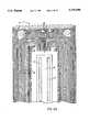
- FIG. 8is a perspective view of the headland area of the inkjet print cartridge of FIG. 7.
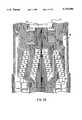
- FIG. 8Ais a perspective view of the headland area of the inkjet print cartridge showing the location of the adhesive bead.
- FIG. 9is a top plan view of the headland area of the inkjet print cartridge of FIG. 7.
- FIG. 9Ais a top plan view of the headland area showing the location of the adhesive bead prior to placing the TAB head assembly on the headland area.
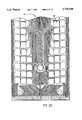
- FIG. 9Bis a side elevational view in cross-section taken along line C--C in FIG. 9 illustrating the configuration of the inner walls and gutter of the headland design.
- FIG. 10is a perspective schematic view of a portion of the inkjet print cartridge of FIG. 3 illustrating the configuration of a seal which is formed between the ink cartridge body and the TAB head assembly.
- FIG. 11is a top perspective view of a substrate structure containing heater resistors, ink channels, and vaporization chambers, which is mounted on the back of the TAB head assembly of FIG. 4.
- FIG. 12is a top perspective view, partially cut away, of a portion of the TAB head assembly showing the relationship of an orifice with respect to a vaporization chamber, a heater resistor, and an edge of the substrate.
- FIG. 13is a schematic cross-sectional view taken along line B--B of FIG. 10 showing the adhesive seal between the TAB head assembly and the print cartridge as well as the ink flow path around the edges of the substrate.
- FIG. 14illustrates one process which may be used to form the preferred TAB head assembly.
- reference numeral 10generally indicates an inkjet print cartridge incorporating a printhead according to one embodiment of the present invention simplified for illustrative purposes.
- the inkjet print cartridge 10includes an ink reservoir 12 and a printhead 14, where the printhead 14 is formed using Tape Automated Bonding (TAB).
- TAB head assembly 14includes a nozzle member 16 comprising two parallel columns of offset holes or orifices 17 formed in a flexible polymer flexible circuit 18 by, for example, laser ablation.
- a back surface of the flexible circuit 18includes conductive traces 36 formed thereon using a conventional photolithographic etching and/or plating process. These conductive traces 36 are terminated by large contact pads 20 designed to interconnect with a printer.
- the print cartridge 10is designed to be installed in a printer so that the contact pads 20, on the front surface of the flexible circuit 18, contact printer electrodes providing externally generated energization signals to the printhead.
- Windows 22 and 24extend through the flexible circuit 18 and are used to facilitate bonding of the other ends of the conductive traces 36 to electrodes on a silicon substrate containing heater resistors.
- the windows 22 and 24are filled with an encapsulant to protect any underlying portion of the traces and substrate.
- the flexible circuit 18is bent over the back edge of the print cartridge "snout" and extends approximately one half the length of the back wall 25 of the snout. This flap portion of the flexible circuit 18 is needed for the routing of conductive traces 36 which are connected to the substrate electrodes through the far end window 22.
- the contact pads 20are located on the flexible circuit 18 which is secured to this wall and the conductive traces 36 are routed over the bend and are connected to the substrate electrodes through the windows 22, 24 in the flexible circuit 18.
- FIG. 2shows a front view of the TAB head assembly 14 of FIG. 1 removed from the print cartridge 10 and prior to windows 22 and 24 in the TAB head assembly 14 being filled with an encapsulant.
- TAB head assembly 14has affixed to the back of the flexible circuit 18 a silicon substrate 28 (not shown) containing a plurality of individually energizable thin film resistors. Each resistor is located generally behind a single orifice 17 and acts as an ohmic heater when selectively energized by one or more pulses applied sequentially or simultaneously to one or more of the contact pads 20.
- the orifices 17 and conductive traces 36may be of any size, number, and pattern, and the various figures are designed to simply and clearly show the features of the invention. The relative dimensions of the various features have been greatly adjusted for the sake of clarity.
- the orifice 17 pattern on the flexible circuit 18 shown in FIG. 2may be formed by a masking process in combination with a laser or other etching means in a step-and-repeat process, which would be readily understood by one of ordinary skilled in the art after reading this disclosure.
- FIG. 14, to be described in detail later,provides additional details of this process. Further details regarding TAB head assembly 14 and flexible circuit 18 are provided below.
- FIG. 3is a perspective view of a simplified schematic of the inkjet print cartridge of FIG. 1 for illustrative purposes.
- FIG. 4is a perspective view of the front surface of the Tape Automated Bonding (TAB) printhead assembly (hereinafter “TAB head assembly”) removed from the simplified schematic print cartridge of FIG. 3.
- TABTape Automated Bonding
- FIG. 5shows the back surface of the TAB head assembly 14 of FIG. 4 showing the silicon die or substrate 28 mounted to the back of the flexible circuit 18 and also showing one edge of the barrier layer 30 formed on the substrate 28 containing ink channels and vaporization chambers.
- FIG. 7shows greater detail of this barrier layer 30 and will be discussed later. Shown along the edge of the barrier layer 30 are the entrances to the ink channels 32 which receive ink from the ink reservoir 12.
- the conductive traces 36 formed on the back of the flexible circuit 18terminate in contact pads 20 (shown in FIG. 4) on the opposite side of the flexible circuit 18.
- the windows 22 and 24allow access to the ends of the conductive traces 36 and the substrate electrodes 40 (shown in FIG. 6) from the other side of the flexible circuit 18 to facilitate bonding.
- FIG. 6shows a side view cross-section taken along line A--A in FIG. 5 illustrating the connection of the ends of the conductive traces 36 to the electrodes 40 formed on the substrate 28.
- a potion 42 of the barrier layer 30is used to insulate the ends of the conductive traces 36 from the substrate 28.
- FIG. 7shows the print cartridge 10 of FIG. 1 with the TAB head assembly 14 removed to reveal the headland design 50 used in providing a seal between the TAB head assembly 14 and the printhead body.
- FIG. 8shows the headland area 50 in enlarged perspective view.
- FIG. 9shows the headland area 50 in an enlarged top plan view. The headland area 50 characteristics are exaggerated for clarity. Shown in FIGS. 8 and 9 is a central slot 52 in the print cartridge 10 for allowing ink from the ink reservoir 12 to flow to the back surface of the TAB head assembly 14.
- the frame geometry, or headland design, 50 formed on the snout of the print cartridge 10is configured so that a bead of epoxy adhesive 90 dispensed along adhesive "V" groove 53 on the inner raised wall 54 and across the wall openings 55 in the inner raised wall and adjacent to and suspended off of adhesive ridges 57 (so as to circumscribe the substrate when the TAB head assembly 14 is in place) will form an ink seal between headland area 50 of the body of the print cartridge 10 and the back of the TAB head assembly 14 when the TAB head assembly 14 is pressed into place against the headland 50.
- FIGS. 8A and 9Ashow the location of the dispensed adhesive.
- FIG. 9Bshows the inner raised wall 54 and gutter 61 in cross-sectional view along sectional line C--C in FIG. 9.
- Other adhesives which may be usedinclude hot-melt, silicone, UV curable adhesive, and mixtures thereof. Further, a patterned adhesive film may be positioned on the headland 50, as opposed to dispensing a bead of adhesive.
- the TAB head assembly 14 of FIG. 5When the TAB head assembly 14 of FIG. 5 is properly positioned and pressed down on the headland design 50 shown in FIGS. 8 and 9 after the adhesive is dispensed (as shown in FIGS. 8A and 9A), the two short ends of the substrate 28 will be supported by the substrate support surface 58. Additional details showing the location of adhesive 90 are shown in FIGS. 10 and 13.
- the configuration of the headland design 50is such that, when the substrate 28 is supported by the substrate support surface 58, the back surface of the flexible circuit 18 will be slightly above the top of the inner raised walls 54 and approximately flush with the flat top surface 59 of the print cartridge 10. As the TAB head assembly 14 is pressed down onto the headland 50, the adhesive is squished down.
- the adhesiveFrom the top of the inner raised walls 54, the adhesive overspills into the gutter 61 between the inner raised walls 54 and the outer raised wall 60. From the wall openings 55 in the inner raised wall, the adhesive squishes upwardly through window 22, 24, squishes inwardly in the direction of spill trough 51 and squishes outwardly toward the outer raised wall 60, which blocks further outward displacement of the adhesive.
- the outward displacement of the adhesivenot only serves as an ink seal, but encapsulates the conductive traces in the vicinity of the windows 22, 24 from underneath to protect the conductive traces from ink.
- the headland design 50 of print cartridge 10utilizes specific unique features to address the difficulty in controlling the adhesive seal of the headland to the TAB head assembly 14.
- a downwardly beveled edge or angled spill trough 51is provided.
- the purpose of this spill trough 51is to allow the excess adhesive to spill downwards onto spill trough 51 if too much adhesive is applied.
- the spill trough 51channels the excess adhesive away from the nozzles 17 and thereby prevents nozzle clogs from forming. This allows the dispensing of a greater variance in adhesive volumes without impairing the functionality of the print cartridge 10. This results in much lower yield losses, greatly reducing the overall manufacturing cost of the print cartridge 10.
- the structural adhesiveis suspended by the protruding edges of the adhesive ridges 57.
- the adhesivesquishes up and partially fills out the back of the windows 22, 24 of the TAB head assembly 14 and then begins to fill up the available area 56 between the adhesive ridges 57.
- no adhesivewill squish through the windows 22, 24 until the available area 56 between the adhesive ridges 57 are all filled with adhesive. Therefore, when a larger volume of adhesive is applied, the open areas 56 between the adhesive ridges 57 begins to fill in without a great increase in adhesive bulge through the windows 22, 24.
- FIG. 10shows a portion of the completed print cartridge 10 of FIG. 3, illustrating in schematic form without headland details, by cross-hatching, the location of the underlying adhesive 90 which forms the adhesive seal between the TAB head assembly 14 and the headland area 50 of the print cartridge 10.
- the adhesiveis located generally between the dashed lines surrounding the array of orifices 17, where the outer dashed line 62 is slightly within the boundaries of the outer raised wall 60 in FIG. 8, and the inner dashed line 64 is slightly within the boundaries of the inner raised walls 54 in FIG. 8.
- the adhesiveis also shown being squished through the wall openings 55 in the inner raised wall (FIGS. 8 and 9) to encapsulate the traces leading to electrodes on the substrate.
- the adhesivealso squishes up through approximately one-half of the windows 22, 24 and flush with the top surface of the windows. A cross-section of this seal taken along line B--B in FIG. 10 is also shown in FIG. 13, to be discussed later.
- This seal formed by the adhesive 90 circumscribing the substrate 28allows ink to flow from slot 52 and around the sides of the substrate to the vaporization chambers formed in the barrier layer 30, but will prevent ink from seeping out from under the TAB head assembly 14.
- this adhesive seal 90provides a strong mechanical coupling of the TAB head assembly 14 to the print cartridge 10, provides a fluidic seal, and provides trace encapsulation.
- the adhesive sealis also easier to cure than prior art seals, and it is much easier to detect leaks between the print cartridge body and the printhead, since the sealant line is readily observable. Further details on adhesive seal 90 are shown in FIG. 13.
- FIG. 11is a front perspective view of the silicon substrate 28 which is affixed to the back of the flexible circuit 18 in FIG. 5 to form the TAB head assembly 14. Silicon substrate 28 has formed on it, using conventional photolithographic techniques, two rows or columns of thin film resistors 70, shown in FIG. 11 exposed through the vaporization chambers 72 formed in the barrier layer 30.
- the substrate 28is approximately one-half inch long and contains 300 heater resistors 70, thus enabling a resolution of 600 dots per inch.
- Heater resistors 70may instead be any other type of ink ejection element, such as a piezoelectric pump-type element or any other conventional element.
- element 70 in all the various figuresmay be considered to be piezoelectric elements in an alternative embodiment without affecting the operation of the printhead.
- electrodes 74are also formed on the substrate 28 for connection to the conductive traces 36 (shown by dashed lines) formed on the back of the flexible circuit 18.
- a demultiplexer 78shown by a dashed outline in FIG. 11, is also formed on the substrate 28 for demultiplexing the incoming multiplexed signals applied to the electrodes 74 and distributing the signals to the various thin film resistors 70.
- the demultiplexer 78enables the use of much fewer electrodes 74 than thin film resistors 70. Having fewer electrodes allows all connections to the substrate to be made from the short end portions of the substrate, as shown in FIG. 4, so that these connections will not interfere with the ink flow around the long sides of the substrate.
- the demultiplexer 78may be any decoder for decoding encoded signals applied to the electrodes 74.
- the demultiplexerhas input leads (not shown for simplicity) connected to the electrodes 74 and has output leads (not shown) connected to the various resistors 70.
- the demultiplexer 78 circuityis discussed in further detail below.
- barrier layer 30which may be a layer of photoresist or some other polymer, in which is formed the vaporization chambers 72 and ink channels 80.
- a portion 42 of the barrier layer 30insulates the conductive traces 36 from the underlying substrate 28, as previously discussed with respect to FIG. 4.
- a thin adhesive layer 84(not shown), such as an uncured layer of poly-isoprene photoresist, is applied to the top surface of the barrier layer 30.
- a separate adhesive layermay not be necessary if the top of the barrier layer 30 can be otherwise made adhesive.
- the resulting substrate structureis then positioned with respect to the back surface of the flexible circuit 18 so as to align the resistors 70 with the orifices formed in the flexible circuit 18.
- This alignment stepalso inherently aligns the electrodes 74 with the ends of the conductive traces 36.
- the traces 36are then bonded to the electrodes 74. This alignment and bonding process is described in more detail later with respect to FIG. 14.
- the aligned and bonded substrate/flexible circuit structureis then heated while applying pressure to cure the adhesive layer 84 and firmly affix the substrate structure to the back surface of the flexible circuit 18.
- FIG. 12is an enlarged view of a single vaporization chamber 72, thin film resistor 70, and frustum shaped orifice 17 after the substrate structure of FIG. 11 is secured to the back of the flexible circuit 18 via the thin adhesive layer 84.
- a side edge of the substrate 28is shown as edge 86.
- inkflows from the ink reservoir 12 around the side edge 86 of the substrate 28, and into the ink channel 80 and associated vaporization chamber 72, as shown by the arrow 88.
- Upon energization of the thin film resistor 70a thin layer of the adjacent ink is superheated, causing explosive vaporization and, consequently, causing a droplet of ink to be ejected through the orifice 17.
- the vaporization chamber 72is then refilled by capillary action.
- the barrier layer 30is approximately 1 mils thick, the substrate 28 is approximately 20 mils thick, and the flexible circuit 18 is approximately 2 mils thick.
- FIG. 13Shown in FIG. 13 is a side elevational view cross-section taken along line B--B in FIG. 10 showing a portion of the adhesive seal 90, applied to the inner raised wall 54 and wall openings 56, surrounding the substrate 28 and showing the substrate 28 being adhesively secured to a central portion of the flexible circuit 18 by the thin adhesive layer 84 on the top surface of the barrier layer 30 containing the ink channels and vaporization chambers 92 and 94.
- FIG. 13also illustrates how ink 88 from the ink reservoir 12 flows through the central slot 52 formed in the print cartridge 10 and flows around the edges 86 of the substrate 28 through ink channels 80 into the vaporization chambers 92 and 94.
- Thin film resistors 96 and 98are shown within the vaporization chambers 92 and 94, respectively. When the resistors 96 and 98 are energized, the ink within the vaporization chambers 92 and 94 are ejected, as illustrated by the emitted drops of ink 101 and 102.
- the edge feed featurewhere ink flows around the edges 86 of the substrate 28 and directly into ink channels 80, has a number of advantages over previous center feed printhead designs which form an elongated central hole or slot running lengthwise in the substrate to allow ink to flow into a central manifold and ultimately to the entrances of ink channels.
- One advantageis that the substrate or die 28 width can be made narrower, due to the absence of the elongated central hole or slot in the substrate. Not only can the substrate be made narrower, but the length of the edge feed substrate can be shorter, for the same number of nozzles, than the center feed substrate due to the substrate structure now being less prone to cracking or breaking without the central ink feed hole.
- This shortening of the substrate 28enables a shorter headland 50 in FIG. 8 and, hence, a shorter print cartridge snout.
- the star wheelscan be located closer to the pinch rollers to ensure better paper/roller contact along the transport path of the print cartridge snout. Additionally, by making the substrate smaller, more substrates can be formed per wafer, thus lowering the material cost per substrate.
- edge feed featuremanufacturing time is saved by not having to etch a slot in the substrate, and the substrate is less prone to breakage during handling. Further, the substrate is able to dissipate more heat, since the ink flowing across the back of the substrate and around the edges of the substrate acts to draw heat away from the back of the substrate.
- the edge feed designBe eliminating the manifold as well as the slot in the substrate, the ink is able to flow more rapidly into the vaporization chambers, since there is less restriction on the ink flow. This more rapid ink flow improves the frequency response of the printhead, allowing higher printing rates from a given number of orifices. Further, the more rapid ink flow reduces crosstalk between nearby vaporization chambers caused by variations in ink flow as the heater elements in the vaporization chambers are fired.
- FIG. 14illustrates one method for forming the preferred embodiment of the TAB head assembly 14.
- the starting materialis a Kapton or Upilex type polymer tape 104, although the tape 104 can be any suitable polymer film which is acceptable for use in the below-described procedure. Some such films may comprise teflon, polyamide, polymethylmethacrylate, polycarbonate, polyester, polyamide polyethylene-terephthalate or mixtures thereof.
- the tape 104is typically provided in long strips on a reel 105.
- Sprocket holes 106 along the sides of the tape 104are used to accurately and securely transport the tape 104.
- the sprocket holes 106may be omitted and the tape may be transported with other types of fixtures.
- the tape 104is already provided with conductive copper traces 36, such as shown in FIGS. 2, 4 and 5, formed thereon using conventional metal deposition and photolithographic processes.
- conductive copper traces 36such as shown in FIGS. 2, 4 and 5, formed thereon using conventional metal deposition and photolithographic processes.
- the particular pattern of conductive tracesdepends on the manner in which it is desired to distribute electrical signals to the electrodes formed on silicon dies, which are subsequently mounted on the tape 104.
- the tape 104is transported to a laser processing chamber and laser-ablated in a pattern defined by one or more masks 108 using laser radiation 110, such as that generated by an Excimer laser 112 of the F 2 , ArF, KrCl, KrF, or XeCl type.
- laser radiation 110such as that generated by an Excimer laser 112 of the F 2 , ArF, KrCl, KrF, or XeCl type.
- the masked laser radiationis designated by arrows 114.
- such masks 108define all of the ablated features for an extended area of the tape 104, for example encompassing multiple orifices in the case of an orifice pattern mask 108, and multiple vaporization chambers in the case of a vaporization chamber pattern mask 108.
- patternssuch as the orifice pattern, the vaporization chamber pattern, or other patterns may be placed side by side on a common mask substrate which is substantially larger than the laser beam. Then such patterns may be moved sequentially into the beam.
- the masking material used in such maskswill preferably be highly reflecting at the laser wavelength, consisting of, for example, a multilayer dielectric or a metal such as aluminum.
- the orifice pattern defined by the one or more masks 108may be that generally shown in FIG. 21. Multiple masks 108 may be used to form a stepped orifice taper as shown in FIG. 12.
- a separate mask 108defines the pattern of windows 22 and 24 shown in FIGS. 1 and 2; however, in the preferred embodiment, the windows 22 and 24 are formed using conventional photolithographic methods prior to the tape 104 being subjected to the processes shown in FIG. 14.
- one or more masks 108would be used to form the orifices and another mask 108 and laser energy level (and/or number of laser shots) would be used to define the vaporization chambers, ink channels, and manifolds which are formed through a portion of the thickness of the tape 104.
- the laser system for this processgenerally includes beam delivery optics, alignment optics, a high precision and high speed mask shuffle system, and a processing chamber including a mechanism for handling and positioning the tape 104.
- the laser systemuses a projection mask configuration wherein a precision lens 115 interposed between the mask 108 and the tape 104 projects the Excimer laser light onto the tape 104 in the image of the pattern defined on the mask 108.
- the masked laser radiation exiting from lens 115is represented by arrows 116.
- Such a projection mask configurationis advantageous for high precision orifice dimensions, because the mask is physically remote from the nozzle member. Soot is naturally formed and ejected in the ablation process, traveling distances of about one centimeter from the nozzle member being ablated. If the mask were in contact with the nozzle member, or in proximity to it, soot buildup on the mask would tend to distort ablated features and reduce their dimensional accuracy. In the preferred embodiment, the projection lens is more than two centimeters from the nozzle member being ablated, thereby avoiding the buildup of any soot on it or on the mask.
- Ablationis well known to produce features with tapered walls, tapered so that the diameter of an orifice is larger at the surface onto which the laser is incident, and smaller at the exit surface.
- the taper anglevaries significantly with variations in the optical energy density incident on the nozzle member for energy densities less than about two joules per square centimeter. If the energy density were uncontrolled, the orifices produced would vary significantly in taper angle, resulting in substantial variations in exit orifice diameter. Such variations would produce deleterious variations in ejected ink drop volume and velocity, reducing print quality.
- the optical energy of the ablating laser beamis precisely monitored and controlled to achieve a consistent taper angle, and thereby a reproducible exit diameter.
- a taperis beneficial to the operation of the orifices, since the taper acts to increase the discharge speed and provide a more focused ejection of ink, as well as provide other advantages.
- the tapermay be in the range of 5 to 15 degrees relative to the axis of the orifice.
- the polymer tape 104is stepped, and the process is repeated. This is referred to as a step-and-repeat process.
- the total processing time required for forming a single pattern on the tape 104may be on the order of a few seconds.
- a single mask patternmay encompass an extended group of ablated features to reduce the processing time per nozzle member.
- Laser ablation processeshave distinct advantages over other forms of laser drilling for the formation of precision orifices, vaporization chambers, and ink channels.
- short pulses of intense ultraviolet lightare absorbed in a thin surface layer of material within about 1 micrometer or less of the surface.
- Preferred pulse energiesare greater than about 100 millijoules per square centimeter and pulse durations are shorter than about 1 microsecond.
- the intense ultraviolet lightphotodissociates the chemical bonds in the material.
- the absorbed ultraviolet energyis concentrated in such a small volume of material that it rapidly heats the dissociated fragments and ejects them away from the surface of the material. Because these processes occur so quickly, there is no time for heat to propagate to the surrounding material.
- laser ablationcan also form chambers with substantially flat bottom surfaces which form a plane recessed into the layer, provided the optical energy density is constant across the region being ablated. The depth of such chambers is determined by the number of laser shots, and the power density of each.
- Laser-ablation processesalso have numerous advantages as compared to conventional lithographic electroforming processes for forming nozzle members for inkjet printheads. For example, laser-ablation processes generally are less expensive and simpler than conventional lithographic electroforming processes.
- polymer nozzle memberscan be fabricated in substantially larger sizes (i.e., having greater surface areas) and with nozzle geometries that are not practical with conventional electroforming processes.
- unique nozzle shapescan be produced by controlling exposure intensity or making multiple exposures with a laser beam being reoriented between each exposure. Examples of a variety of nozzle shapes are described in co-pending application Ser. No.
- nozzle membersby laser-ablating a polymer material
- Lnozzle length
- Dnozzle diameter
- L/D ratioexceeds unity.
- One advantage of extending a nozzle's length relative to its diameteris that orifice-resistor positioning in a vaporization chamber becomes less critical.
- laser-ablated polymer nozzle members for inkjet printershave characteristics that are superior to conventional electroformed orifice plates.
- laser-ablated polymer nozzle membersare highly resistant to corrosion by water-based printing inks and are generally hydrophobic.
- laser-ablated polymer nozzle membershave a relatively low elastic modules, so built-in stress between the nozzle member and an underlying substrate or barrier layer has less of a tendency to cause nozzle member-to-barrier layer delamination.
- laser-ablated polymer nozzle memberscan be readily fixed to, or formed with, a polymer substrate.
- the wavelength of such an ultraviolet light sourcewill lie in the 150 nm to 400 nm range to allow high absorption in the tape to be ablated.
- the energy densityshould be greater than about 100 millijoules per square centimeter with a pulse length shorter than about 1 microsecond to achieve rapid ejection of ablated material with essentially no heating of the surrounding remaining material.
- a next step in the processis a cleaning step wherein the laser ablated portion of the tape 104 is positioned under a cleaning station 117. At the cleaning station 117, debris from the laser ablation is removed according to standard industry practice.
- the tape 104is then stepped to the next station, which is an optical alignment station 118 incorporated in a conventional automatic TAB bonder, such as an inner lead bonder commercially available from Shinkawa Corporation, model number IL-20.
- the bonderis preprogrammed with an alignment (target) pattern on the nozzle member, created in the same manner and/or step as used to created the orifices, and a target pattern on the substrate, created in the same manner and/or step used to create the resistors.
- the nozzle member materialis semi-transparent so that the target pattern on the substrate may be viewed through the nozzle member.
- the bonderthen automatically positions the silicon dies 120 with respect to the nozzle members so as to align the two target patterns.
- the alignment of the silicon dies 120 with respect to the tape 104is performed automatically using only commercially available equipment.
- By integrating the conductive traces with the nozzle member, such an alignment featureis possible.
- Such integrationnot only reduces the assembly cost of the printhead but reduces the printhead material cost as well.
- the automatic TAB bonderthen uses a gang bonding method to press the ends of the conductive traces down onto the associated substrate electrodes through the windows formed in the tape 104.
- the bonderthen applies heat, such as by using thermo-compression bonding, to weld the ends of the traces to the associated electrodes.
- a schematic side view of one embodiment of the resulting structureis shown in FIG. 6.
- Other types of bondingcan also be used, such as ultrasonic bonding, conductive epoxy, solder paste, or other well-known means.
- the tape 104is then stepped to a heat and pressure station 122.
- an adhesive layer 84exists on the top surface of the barrier layer 30 formed on the silicon substrate.
- the silicon dies 120are then pressed down against the tape 104, and heat is applied to cure the adhesive layer 84 and physically bond the dies 120 to the tape 104.
- the tape 104steps and is optionally taken up on the take-up reel 124.
- the tape 104may then later be cut to separate the individual TAB head assemblies from one another.
- the resulting TAB head assemblyis then positioned on the print cartridge 10, and the previously described adhesive seal 90 is formed to firmly secure the nozzle member to the print cartridge, provide an ink-proof seal around the substrate between the nozzle member and the ink reservoir, and encapsulate the traces in the vicinity of the headland so as to isolate the traces from the ink.
- Peripheral points on the flexible TAB head assemblyare then secured to the plastic print cartridge 10 by a conventional melt-through type bonding process to cause the polymer flexible circuit 18 to remain relatively flush with the surface of the print cartridge 10, as shown in FIG. 1.
Landscapes
- Engineering & Computer Science (AREA)
- Manufacturing & Machinery (AREA)
- Physics & Mathematics (AREA)
- Optics & Photonics (AREA)
- Particle Formation And Scattering Control In Inkjet Printers (AREA)
Abstract
Description
Claims (24)
Priority Applications (2)
| Application Number | Priority Date | Filing Date | Title |
|---|---|---|---|
| US08/398,849US5736998A (en) | 1995-03-06 | 1995-03-06 | Inkjet cartridge design for facilitating the adhesive sealing of a printhead to an ink reservoir |
| US08/655,796US5852460A (en) | 1995-03-06 | 1996-05-31 | Inkjet print cartridge design to decrease deformation of the printhead when adhesively sealing the printhead to the print cartridge |
Applications Claiming Priority (1)
| Application Number | Priority Date | Filing Date | Title |
|---|---|---|---|
| US08/398,849US5736998A (en) | 1995-03-06 | 1995-03-06 | Inkjet cartridge design for facilitating the adhesive sealing of a printhead to an ink reservoir |
Related Child Applications (1)
| Application Number | Title | Priority Date | Filing Date |
|---|---|---|---|
| US08/655,796Continuation-In-PartUS5852460A (en) | 1995-03-06 | 1996-05-31 | Inkjet print cartridge design to decrease deformation of the printhead when adhesively sealing the printhead to the print cartridge |
Publications (1)
| Publication Number | Publication Date |
|---|---|
| US5736998Atrue US5736998A (en) | 1998-04-07 |
Family
ID=23577035
Family Applications (1)
| Application Number | Title | Priority Date | Filing Date |
|---|---|---|---|
| US08/398,849Expired - LifetimeUS5736998A (en) | 1995-03-06 | 1995-03-06 | Inkjet cartridge design for facilitating the adhesive sealing of a printhead to an ink reservoir |
Country Status (1)
| Country | Link |
|---|---|
| US (1) | US5736998A (en) |
Cited By (45)
| Publication number | Priority date | Publication date | Assignee | Title |
|---|---|---|---|---|
| US6190002B1 (en) | 1999-10-27 | 2001-02-20 | Lexmark International, Inc. | Ink jet pen |
| US6244696B1 (en) | 1999-04-30 | 2001-06-12 | Hewlett-Packard Company | Inkjet print cartridge design for decreasing ink shorts by using an elevated substrate support surface to increase adhesive sealing of the printhead from ink penetration |
| US6276779B1 (en)* | 1999-11-24 | 2001-08-21 | Xerox Corporation | Acoustic fluid emission head and method of forming same |
| US6318843B1 (en)* | 1997-10-23 | 2001-11-20 | Hewlett-Packard Company | Control of adhesive flow in an inkjet printer printhead |
| US6322200B1 (en) | 1999-10-29 | 2001-11-27 | Hewlett-Packard Company | Decoupled nozzle plate and electrical flexible circuit for an inkjet print cartridge |
| US6325491B1 (en) | 1999-10-30 | 2001-12-04 | Hewlett-Packard Company | Inkjet printhead design to reduce corrosion of substrate bond pads |
| EP1087871A4 (en)* | 1998-06-19 | 2001-12-19 | Lexmark Int Inc | CHIP MODULE WITH A HEART ELEMENT FOR INK JET PRINTERS |
| EP1138495A3 (en)* | 2000-03-31 | 2002-01-16 | Canon Kabushiki Kaisha | Liquid discharge recording head, method of manufacture therefor, and liquid discharge recording apparatus |
| US6361160B2 (en)* | 1999-04-30 | 2002-03-26 | Hewlett Packard Company | Print cartridge with adhesive dispensed through window of flexible circuit |
| US6371597B1 (en) | 2000-01-20 | 2002-04-16 | Lexmark International, Inc. | Tab circuit to minimize corrosion due to ink |
| US6378984B1 (en) | 1998-07-31 | 2002-04-30 | Hewlett-Packard Company | Reinforcing features in flex circuit to provide improved performance in a thermal inkjet printhead |
| US6402299B1 (en) | 1999-10-22 | 2002-06-11 | Lexmark International, Inc. | Tape automated bonding circuit for use with an ink jet cartridge assembly in an ink jet printer |
| US6439698B1 (en)* | 2000-01-14 | 2002-08-27 | Lexmark International, Inc | Dual curable encapsulating material |
| US6461812B2 (en) | 1998-09-09 | 2002-10-08 | Agilent Technologies, Inc. | Method and multiple reservoir apparatus for fabrication of biomolecular arrays |
| US6473966B1 (en)* | 1999-02-01 | 2002-11-05 | Casio Computer Co., Ltd. | Method of manufacturing ink-jet printer head |
| US6612032B1 (en)* | 2000-01-31 | 2003-09-02 | Lexmark International, Inc. | Manufacturing method for ink jet pen |
| US6619786B2 (en) | 2001-06-08 | 2003-09-16 | Lexmark International, Inc. | Tab circuit for ink jet printer cartridges |
| EP1354705A1 (en)* | 2002-04-19 | 2003-10-22 | Sony Corporation | Liquid discharge apparatus, printer head, and method for making liquid discharge apparatus |
| US6663235B2 (en) | 2001-10-31 | 2003-12-16 | Hewlett-Packard Development Company, L.P. | Coverlayer based on functional polymers |
| US20040087063A1 (en)* | 2002-10-31 | 2004-05-06 | Mohammad Akhavin | Edge-sealed substrates and methods for effecting the same |
| US20050073552A1 (en)* | 2003-10-03 | 2005-04-07 | Smoot Mary C. | Method of applying an encapsulant material to an ink jet printhead |
| US20060001703A1 (en)* | 2004-06-30 | 2006-01-05 | Bertelsen Craig M | Die attach methods and apparatus for micro-fluid ejection device |
| US20060001713A1 (en)* | 2004-06-30 | 2006-01-05 | Kwan Kin M | Inkjet print cartridge having an adhesive with improved dimensional control |
| US7043838B2 (en) | 2004-06-30 | 2006-05-16 | Lexmark International, Inc. | Process for manufacturing a micro-fluid ejection device |
| US20060139410A1 (en)* | 2004-12-08 | 2006-06-29 | Canon Kabushiki Kaisha | Liquid discharge recording head and ink jet recording apparatus |
| US7165831B2 (en) | 2004-08-19 | 2007-01-23 | Lexmark International, Inc. | Micro-fluid ejection devices |
| US20070093001A1 (en)* | 2005-10-24 | 2007-04-26 | Garcia Carlos B | Encapsulating electrical connections |
| US20070112095A1 (en)* | 2005-10-28 | 2007-05-17 | Canon Kabushiki Kaisha | Aqueous ink, ink jet recording method, ink cartridge, recording unit and ink jet recording apparatus |
| US20070146411A1 (en)* | 2005-12-22 | 2007-06-28 | Robertson Douglas L | Maintenance on a hand-held printer |
| US20070206067A1 (en)* | 2006-03-01 | 2007-09-06 | Lexmark International, Inc. | Internal vent channel in ejection head assemblies and methods relating thereto |
| US7399052B1 (en)* | 2005-03-25 | 2008-07-15 | Anderson Stephen A | Renovated ink jet cartridge and method of renovating |
| US20080269389A1 (en)* | 2004-03-05 | 2008-10-30 | Mikio Shiono | Fluoropolyether adhesive composition |
| US20090229126A1 (en)* | 2008-03-17 | 2009-09-17 | Seiko Epson Corporation | Method for manufacturing liquid jet head |
| US20100043533A1 (en)* | 2008-08-19 | 2010-02-25 | Silverbrook Research Pty Ltd | Pneumatic assembly for a pressure decay tester |
| US20100043536A1 (en)* | 2008-08-19 | 2010-02-25 | Silverbrook Research Pty Ltd | Cradle assembly for a pressure decay leak tester |
| US20110025784A1 (en)* | 2008-05-15 | 2011-02-03 | Marrow Michael M | Flexible Circuit Seal |
| US20110033660A1 (en)* | 2008-04-18 | 2011-02-10 | Yi Feng | Adhesive Tape for use with a Polymer Substrate |
| US7895247B2 (en) | 2003-10-29 | 2011-02-22 | Oracle International Corporation | Tracking space usage in a database |
| US20110079223A1 (en)* | 2004-09-27 | 2011-04-07 | Canon Kabushiki Kaisha | Ejection liquid, ejection method, method for forming liquid droplets, liquid ejection cartridge and ejection apparatus |
| US7926916B2 (en)* | 2002-01-31 | 2011-04-19 | Hewlett-Packard Development Company, L.P. | Adhesive joint with an ink trap and method |
| US20110141204A1 (en)* | 2009-12-15 | 2011-06-16 | Xerox Corporation | Print Head Having a Polymer Layer to Facilitate Assembly of the Print Head |
| US20110148994A1 (en)* | 2009-12-17 | 2011-06-23 | Xerox Corporation | Print Head Having a Polymer Aperture Plate and Method for Assembling a Print Head |
| US20110232371A1 (en)* | 2008-08-19 | 2011-09-29 | Silverbrook Research Pty Ltd | Pressure tester for printhead integrated circuit carrier |
| US9421771B2 (en)* | 2014-05-12 | 2016-08-23 | Canon Kabushiki Kaisha | Liquid ejection head and method of manufacturing the same |
| US11225070B2 (en) | 2018-01-23 | 2022-01-18 | Hewlett-Packard Development Company, L.P. | Fluidic dies with beveled edges underneath electrical leads |
Citations (29)
| Publication number | Priority date | Publication date | Assignee | Title |
|---|---|---|---|---|
| US4312009A (en)* | 1979-02-16 | 1982-01-19 | Smh-Adrex | Device for projecting ink droplets onto a medium |
| US4450455A (en)* | 1981-06-18 | 1984-05-22 | Canon Kabushiki Kaisha | Ink jet head |
| US4490728A (en)* | 1981-08-14 | 1984-12-25 | Hewlett-Packard Company | Thermal ink jet printer |
| US4500895A (en)* | 1983-05-02 | 1985-02-19 | Hewlett-Packard Company | Disposable ink jet head |
| US4502060A (en)* | 1983-05-02 | 1985-02-26 | Hewlett-Packard Company | Barriers for thermal ink jet printers |
| US4550326A (en)* | 1983-05-02 | 1985-10-29 | Hewlett-Packard Company | Fluidic tuning of impulse jet devices using passive orifices |
| US4558333A (en)* | 1981-07-09 | 1985-12-10 | Canon Kabushiki Kaisha | Liquid jet recording head |
| US4568953A (en)* | 1982-12-28 | 1986-02-04 | Canon Kabushiki Kaisha | Liquid injection recording apparatus |
| US4580149A (en)* | 1985-02-19 | 1986-04-01 | Xerox Corporation | Cavitational liquid impact printer |
| US4587534A (en)* | 1983-01-28 | 1986-05-06 | Canon Kabushiki Kaisha | Liquid injection recording apparatus |
| US4611219A (en)* | 1981-12-29 | 1986-09-09 | Canon Kabushiki Kaisha | Liquid-jetting head |
| JPS62170350A (en)* | 1986-01-24 | 1987-07-27 | Mitsubishi Electric Corp | Recorder |
| US4683481A (en)* | 1985-12-06 | 1987-07-28 | Hewlett-Packard Company | Thermal ink jet common-slotted ink feed printhead |
| US4695854A (en)* | 1986-07-30 | 1987-09-22 | Pitney Bowes Inc. | External manifold for ink jet array |
| US4712172A (en)* | 1984-04-17 | 1987-12-08 | Canon Kabushiki Kaisha | Method for preventing non-discharge in a liquid jet recorder and a liquid jet recorder |
| US4734717A (en)* | 1986-12-22 | 1988-03-29 | Eastman Kodak Company | Insertable, multi-array print/cartridge |
| US4746935A (en)* | 1985-11-22 | 1988-05-24 | Hewlett-Packard Company | Multitone ink jet printer and method of operation |
| US4773971A (en)* | 1986-10-30 | 1988-09-27 | Hewlett-Packard Company | Thin film mandrel |
| US4780177A (en)* | 1988-02-05 | 1988-10-25 | General Electric Company | Excimer laser patterning of a novel resist |
| US4842677A (en)* | 1988-02-05 | 1989-06-27 | General Electric Company | Excimer laser patterning of a novel resist using masked and maskless process steps |
| US4847630A (en)* | 1987-12-17 | 1989-07-11 | Hewlett-Packard Company | Integrated thermal ink jet printhead and method of manufacture |
| US4915981A (en)* | 1988-08-12 | 1990-04-10 | Rogers Corporation | Method of laser drilling fluoropolymer materials |
| EP0367541A2 (en)* | 1988-10-31 | 1990-05-09 | Canon Kabushiki Kaisha | Method of manufacturing an ink jet head |
| US4926197A (en)* | 1988-03-16 | 1990-05-15 | Hewlett-Packard Company | Plastic substrate for thermal ink jet printer |
| US4942408A (en)* | 1989-04-24 | 1990-07-17 | Eastman Kodak Company | Bubble ink jet print head and cartridge construction and fabrication method |
| EP0309146B1 (en)* | 1987-09-19 | 1993-01-13 | Xaar Limited | Manufacture of nozzles for ink jet printers |
| US5198834A (en)* | 1991-04-02 | 1993-03-30 | Hewlett-Packard Company | Ink jet print head having two cured photoimaged barrier layers |
| US5278584A (en)* | 1992-04-02 | 1994-01-11 | Hewlett-Packard Company | Ink delivery system for an inkjet printhead |
| US5484500A (en)* | 1990-10-09 | 1996-01-16 | E. I. Du Pont De Nemours And Company | Method for forming structural panels having a core with thermoplastic resin facings |
- 1995
- 1995-03-06USUS08/398,849patent/US5736998A/ennot_activeExpired - Lifetime
Patent Citations (29)
| Publication number | Priority date | Publication date | Assignee | Title |
|---|---|---|---|---|
| US4312009A (en)* | 1979-02-16 | 1982-01-19 | Smh-Adrex | Device for projecting ink droplets onto a medium |
| US4450455A (en)* | 1981-06-18 | 1984-05-22 | Canon Kabushiki Kaisha | Ink jet head |
| US4558333A (en)* | 1981-07-09 | 1985-12-10 | Canon Kabushiki Kaisha | Liquid jet recording head |
| US4490728A (en)* | 1981-08-14 | 1984-12-25 | Hewlett-Packard Company | Thermal ink jet printer |
| US4611219A (en)* | 1981-12-29 | 1986-09-09 | Canon Kabushiki Kaisha | Liquid-jetting head |
| US4568953A (en)* | 1982-12-28 | 1986-02-04 | Canon Kabushiki Kaisha | Liquid injection recording apparatus |
| US4587534A (en)* | 1983-01-28 | 1986-05-06 | Canon Kabushiki Kaisha | Liquid injection recording apparatus |
| US4500895A (en)* | 1983-05-02 | 1985-02-19 | Hewlett-Packard Company | Disposable ink jet head |
| US4502060A (en)* | 1983-05-02 | 1985-02-26 | Hewlett-Packard Company | Barriers for thermal ink jet printers |
| US4550326A (en)* | 1983-05-02 | 1985-10-29 | Hewlett-Packard Company | Fluidic tuning of impulse jet devices using passive orifices |
| US4712172A (en)* | 1984-04-17 | 1987-12-08 | Canon Kabushiki Kaisha | Method for preventing non-discharge in a liquid jet recorder and a liquid jet recorder |
| US4580149A (en)* | 1985-02-19 | 1986-04-01 | Xerox Corporation | Cavitational liquid impact printer |
| US4746935A (en)* | 1985-11-22 | 1988-05-24 | Hewlett-Packard Company | Multitone ink jet printer and method of operation |
| US4683481A (en)* | 1985-12-06 | 1987-07-28 | Hewlett-Packard Company | Thermal ink jet common-slotted ink feed printhead |
| JPS62170350A (en)* | 1986-01-24 | 1987-07-27 | Mitsubishi Electric Corp | Recorder |
| US4695854A (en)* | 1986-07-30 | 1987-09-22 | Pitney Bowes Inc. | External manifold for ink jet array |
| US4773971A (en)* | 1986-10-30 | 1988-09-27 | Hewlett-Packard Company | Thin film mandrel |
| US4734717A (en)* | 1986-12-22 | 1988-03-29 | Eastman Kodak Company | Insertable, multi-array print/cartridge |
| EP0309146B1 (en)* | 1987-09-19 | 1993-01-13 | Xaar Limited | Manufacture of nozzles for ink jet printers |
| US4847630A (en)* | 1987-12-17 | 1989-07-11 | Hewlett-Packard Company | Integrated thermal ink jet printhead and method of manufacture |
| US4842677A (en)* | 1988-02-05 | 1989-06-27 | General Electric Company | Excimer laser patterning of a novel resist using masked and maskless process steps |
| US4780177A (en)* | 1988-02-05 | 1988-10-25 | General Electric Company | Excimer laser patterning of a novel resist |
| US4926197A (en)* | 1988-03-16 | 1990-05-15 | Hewlett-Packard Company | Plastic substrate for thermal ink jet printer |
| US4915981A (en)* | 1988-08-12 | 1990-04-10 | Rogers Corporation | Method of laser drilling fluoropolymer materials |
| EP0367541A2 (en)* | 1988-10-31 | 1990-05-09 | Canon Kabushiki Kaisha | Method of manufacturing an ink jet head |
| US4942408A (en)* | 1989-04-24 | 1990-07-17 | Eastman Kodak Company | Bubble ink jet print head and cartridge construction and fabrication method |
| US5484500A (en)* | 1990-10-09 | 1996-01-16 | E. I. Du Pont De Nemours And Company | Method for forming structural panels having a core with thermoplastic resin facings |
| US5198834A (en)* | 1991-04-02 | 1993-03-30 | Hewlett-Packard Company | Ink jet print head having two cured photoimaged barrier layers |
| US5278584A (en)* | 1992-04-02 | 1994-01-11 | Hewlett-Packard Company | Ink delivery system for an inkjet printhead |
Non-Patent Citations (13)
| Title |
|---|
| Gary L. Seiwell, et al., "The ThinkJet Orifice Plate: A Part With Many Functions," May 1985, Hewlett-Packard Journal, pp. 33-37. |
| Gary L. Seiwell, et al., The ThinkJet Orifice Plate: A Part With Many Functions, May 1985, Hewlett Packard Journal, pp. 33 37.* |
| J. I. Crowley, et al., Nozzles For Ink Jet Printers, IBM Technical Disclosure Bulletin, vol. 25, No. 8, Jan. 1983.* |
| J. T. C. Yeh, "Laser Ablation Of Polymers," J. Vac. Sci. Tech. May/Jun. 86, pp. 653-658. |
| J. T. C. Yeh, Laser Ablation Of Polymers, J. Vac. Sci. Tech. May/Jun. 86, pp. 653 658.* |
| Nielsen, Niels J., "History of ThinkJet Printhead Development," Hewlett-Packard Journal, May 1985, pp. 4-7. |
| Nielsen, Niels J., History of ThinkJet Printhead Development, Hewlett Packard Journal, May 1985, pp. 4 7.* |
| R. Srinivasan, et al., "Self-Developing Photoetching Of Poly(ethylene terephthalate) Films by Far-Ultraviiolet Excimer Laser Radiation," IBM Thomas J. Watson Research Center, Yorktown Heights, New York; recieved May 10, 1982; accepted for publication Jul. 2, 1982. |
| R. Srinivasan, et al., Self Developing Photoetching Of Poly(ethylene terephthalate) Films by Far Ultraviiolet Excimer Laser Radiation, IBM Thomas J. Watson Research Center, Yorktown Heights, New York; recieved May 10, 1982; accepted for publication Jul. 2, 1982.* |
| R. Srinivasan, Kinetics of the Ablative Photodecomposition of Organic Polymers in the Far Ultraviolet, IBM Thomas J. Watson Research Center, Yorktown Heights, New York; received Mar. 21, 1983; accepted for publication Jun. 24, 1983.* |
| Thomas A. Znotins, et al., "Excimer Lasers: An Emerging Technology in Materials Processing," Laser Focus Electro Optics, May 1987, pp. 54-70. |
| Thomas A. Znotins, et al., Excimer Lasers: An Emerging Technology in Materials Processing, Laser Focus Electro Optics, May 1987, pp. 54 70.* |
| V. Srinivasan, et al., Excimer Laser Etching Of Polymers, Department of Chemical Engineering, Clarkson University, Potsdam, New York, received Dec. 30, 1985; accepted for publication, Feb. 19, 1986.* |
Cited By (81)
| Publication number | Priority date | Publication date | Assignee | Title |
|---|---|---|---|---|
| US6318843B1 (en)* | 1997-10-23 | 2001-11-20 | Hewlett-Packard Company | Control of adhesive flow in an inkjet printer printhead |
| EP1087871A4 (en)* | 1998-06-19 | 2001-12-19 | Lexmark Int Inc | CHIP MODULE WITH A HEART ELEMENT FOR INK JET PRINTERS |
| US6378984B1 (en) | 1998-07-31 | 2002-04-30 | Hewlett-Packard Company | Reinforcing features in flex circuit to provide improved performance in a thermal inkjet printhead |
| US20040002072A1 (en)* | 1998-09-09 | 2004-01-01 | Barth Phillip W | Method and multiple reservoir apparatus for fabrication of biomolecular arrays |
| US6461812B2 (en) | 1998-09-09 | 2002-10-08 | Agilent Technologies, Inc. | Method and multiple reservoir apparatus for fabrication of biomolecular arrays |
| US7026124B2 (en) | 1998-09-09 | 2006-04-11 | Agilent Technologies, Inc. | Method and multiple reservoir apparatus for fabrication of biomolecular arrays |
| US6473966B1 (en)* | 1999-02-01 | 2002-11-05 | Casio Computer Co., Ltd. | Method of manufacturing ink-jet printer head |
| US6244696B1 (en) | 1999-04-30 | 2001-06-12 | Hewlett-Packard Company | Inkjet print cartridge design for decreasing ink shorts by using an elevated substrate support surface to increase adhesive sealing of the printhead from ink penetration |
| US6361160B2 (en)* | 1999-04-30 | 2002-03-26 | Hewlett Packard Company | Print cartridge with adhesive dispensed through window of flexible circuit |
| US6364475B2 (en) | 1999-04-30 | 2002-04-02 | Hewlett-Packard Company | Inkjet print cartridge design to decrease ink shorts due to ink penetration of the printhead |
| US6402299B1 (en) | 1999-10-22 | 2002-06-11 | Lexmark International, Inc. | Tape automated bonding circuit for use with an ink jet cartridge assembly in an ink jet printer |
| US6190002B1 (en) | 1999-10-27 | 2001-02-20 | Lexmark International, Inc. | Ink jet pen |
| US6322200B1 (en) | 1999-10-29 | 2001-11-27 | Hewlett-Packard Company | Decoupled nozzle plate and electrical flexible circuit for an inkjet print cartridge |
| US6325491B1 (en) | 1999-10-30 | 2001-12-04 | Hewlett-Packard Company | Inkjet printhead design to reduce corrosion of substrate bond pads |
| US6276779B1 (en)* | 1999-11-24 | 2001-08-21 | Xerox Corporation | Acoustic fluid emission head and method of forming same |
| US6439698B1 (en)* | 2000-01-14 | 2002-08-27 | Lexmark International, Inc | Dual curable encapsulating material |
| US6371597B1 (en) | 2000-01-20 | 2002-04-16 | Lexmark International, Inc. | Tab circuit to minimize corrosion due to ink |
| US6612032B1 (en)* | 2000-01-31 | 2003-09-02 | Lexmark International, Inc. | Manufacturing method for ink jet pen |
| US7018503B2 (en) | 2000-01-31 | 2006-03-28 | Lexmark International, Inc. | Manufacturing method for ink jet pen |
| US20030188827A1 (en)* | 2000-01-31 | 2003-10-09 | Ashok Murthy | Manufacturing method for ink jet pen |
| US6626514B2 (en) | 2000-03-31 | 2003-09-30 | Canon Kabushiki Kaisha | Liquid discharge recording head, method of manufacture therefor, and liquid discharge recording apparatus |
| EP1138495A3 (en)* | 2000-03-31 | 2002-01-16 | Canon Kabushiki Kaisha | Liquid discharge recording head, method of manufacture therefor, and liquid discharge recording apparatus |
| US6619786B2 (en) | 2001-06-08 | 2003-09-16 | Lexmark International, Inc. | Tab circuit for ink jet printer cartridges |
| US6663235B2 (en) | 2001-10-31 | 2003-12-16 | Hewlett-Packard Development Company, L.P. | Coverlayer based on functional polymers |
| US7926916B2 (en)* | 2002-01-31 | 2011-04-19 | Hewlett-Packard Development Company, L.P. | Adhesive joint with an ink trap and method |
| US20050248614A1 (en)* | 2002-04-19 | 2005-11-10 | Sony Corporation | Liquid discharge apparatus, printer head, and method for making liquid discharge apparatus |
| US20050231552A1 (en)* | 2002-04-19 | 2005-10-20 | Sony Corporation | Liquid discharge apparatus, printer head, and method for making liquid discharge apparatus |
| SG115537A1 (en)* | 2002-04-19 | 2005-10-28 | Sony Corp | Liquid discharge apparatus, printer head, and method for making liquid discharge apparatus |
| US20050253896A1 (en)* | 2002-04-19 | 2005-11-17 | Sony Corporation | Liquid discharge apparatus, printer head, and method for making liquid discharge apparatus |
| US20050275688A1 (en)* | 2002-04-19 | 2005-12-15 | Sony Corporation | Liquid discharge apparatus, printer head, and method for making liquid discharge apparatus |
| US7165828B2 (en) | 2002-04-19 | 2007-01-23 | Sony Corporation | Liquid discharge apparatus, printer head, and method for making liquid discharge apparatus |
| US7090330B2 (en) | 2002-04-19 | 2006-08-15 | Sony Corporation | Liquid discharge apparatus, printer head, and method for making liquid discharge apparatus |
| US7004561B2 (en) | 2002-04-19 | 2006-02-28 | Sony Corporation | Liquid discharge apparatus, printer head, and method for making liquid discharge apparatus |
| US20040021736A1 (en)* | 2002-04-19 | 2004-02-05 | Takaaki Murakami | Liquid discharge apparatus, printer head, and method for making liquid discharge apparatus |
| EP1354705A1 (en)* | 2002-04-19 | 2003-10-22 | Sony Corporation | Liquid discharge apparatus, printer head, and method for making liquid discharge apparatus |
| US6951778B2 (en) | 2002-10-31 | 2005-10-04 | Hewlett-Packard Development Company, L.P. | Edge-sealed substrates and methods for effecting the same |
| US20040087063A1 (en)* | 2002-10-31 | 2004-05-06 | Mohammad Akhavin | Edge-sealed substrates and methods for effecting the same |
| US7121647B2 (en) | 2003-10-03 | 2006-10-17 | Lexmark International, Inc. | Method of applying an encapsulant material to an ink jet printhead |
| US20050073552A1 (en)* | 2003-10-03 | 2005-04-07 | Smoot Mary C. | Method of applying an encapsulant material to an ink jet printhead |
| US7895247B2 (en) | 2003-10-29 | 2011-02-22 | Oracle International Corporation | Tracking space usage in a database |
| US7855256B2 (en)* | 2004-03-05 | 2010-12-21 | Shin-Etsu Chemical Co., Ltd. | Fluoropolyether adhesive composition |
| US20080269389A1 (en)* | 2004-03-05 | 2008-10-30 | Mikio Shiono | Fluoropolyether adhesive composition |
| US7311386B2 (en) | 2004-06-30 | 2007-12-25 | Lexmark Interntional, Inc. | Die attach methods and apparatus for micro-fluid ejection device |
| US20060001703A1 (en)* | 2004-06-30 | 2006-01-05 | Bertelsen Craig M | Die attach methods and apparatus for micro-fluid ejection device |
| US20060001713A1 (en)* | 2004-06-30 | 2006-01-05 | Kwan Kin M | Inkjet print cartridge having an adhesive with improved dimensional control |
| US7404613B2 (en) | 2004-06-30 | 2008-07-29 | Lexmark International, Inc. | Inkjet print cartridge having an adhesive with improved dimensional control |
| US7043838B2 (en) | 2004-06-30 | 2006-05-16 | Lexmark International, Inc. | Process for manufacturing a micro-fluid ejection device |
| US7165831B2 (en) | 2004-08-19 | 2007-01-23 | Lexmark International, Inc. | Micro-fluid ejection devices |
| US8833363B2 (en)* | 2004-09-27 | 2014-09-16 | Canon Kabushiki Kaisha | Ejection liquid, ejection method, method for forming liquid droplets, liquid ejection cartridge and ejection apparatus |
| US20110079223A1 (en)* | 2004-09-27 | 2011-04-07 | Canon Kabushiki Kaisha | Ejection liquid, ejection method, method for forming liquid droplets, liquid ejection cartridge and ejection apparatus |
| US20060139410A1 (en)* | 2004-12-08 | 2006-06-29 | Canon Kabushiki Kaisha | Liquid discharge recording head and ink jet recording apparatus |
| EP1833678A4 (en)* | 2004-12-08 | 2009-04-22 | Canon Kk | Liquid discharge recording head and ink jet recording device |
| US7399052B1 (en)* | 2005-03-25 | 2008-07-15 | Anderson Stephen A | Renovated ink jet cartridge and method of renovating |
| US20070093001A1 (en)* | 2005-10-24 | 2007-04-26 | Garcia Carlos B | Encapsulating electrical connections |
| US7691675B2 (en) | 2005-10-24 | 2010-04-06 | Hewlett-Packard Development Company, L.P. | Encapsulating electrical connections |
| US8367750B2 (en)* | 2005-10-28 | 2013-02-05 | Canon Kabushiki Kaisha | Aqueous ink, ink jet recording method, ink cartridge, recording unit and ink jet recording apparatus |
| US8741984B2 (en) | 2005-10-28 | 2014-06-03 | Canon Kabushiki Kaisha | Aqueous ink, ink jet recording method, ink cartridge, recording unit and ink jet recording apparatus |
| US20070112095A1 (en)* | 2005-10-28 | 2007-05-17 | Canon Kabushiki Kaisha | Aqueous ink, ink jet recording method, ink cartridge, recording unit and ink jet recording apparatus |
| WO2007075353A3 (en)* | 2005-12-22 | 2008-04-10 | Lexmark Int Inc | Maintenance on an hand-held printer |
| US7604320B2 (en) | 2005-12-22 | 2009-10-20 | Lexmark International, Inc. | Maintenance on a hand-held printer |
| US20070146411A1 (en)* | 2005-12-22 | 2007-06-28 | Robertson Douglas L | Maintenance on a hand-held printer |
| US7600850B2 (en)* | 2006-03-01 | 2009-10-13 | Lexmark International, Inc. | Internal vent channel in ejection head assemblies and methods relating thereto |
| US20070206067A1 (en)* | 2006-03-01 | 2007-09-06 | Lexmark International, Inc. | Internal vent channel in ejection head assemblies and methods relating thereto |
| US7996991B2 (en)* | 2008-03-17 | 2011-08-16 | Seiko Epson Corporation | Method for manufacturing liquid jet head |
| US20090229126A1 (en)* | 2008-03-17 | 2009-09-17 | Seiko Epson Corporation | Method for manufacturing liquid jet head |
| US20110033660A1 (en)* | 2008-04-18 | 2011-02-10 | Yi Feng | Adhesive Tape for use with a Polymer Substrate |
| US20110025784A1 (en)* | 2008-05-15 | 2011-02-03 | Marrow Michael M | Flexible Circuit Seal |
| US9056470B2 (en)* | 2008-05-15 | 2015-06-16 | Hewlett-Packard Development Company, L.P. | Flexible circuit seal |
| US8006967B2 (en)* | 2008-08-19 | 2011-08-30 | Silverbrook Research Pty Ltd | Cradle assembly for a pressure decay leak tester |
| US20100043536A1 (en)* | 2008-08-19 | 2010-02-25 | Silverbrook Research Pty Ltd | Cradle assembly for a pressure decay leak tester |
| US20110232371A1 (en)* | 2008-08-19 | 2011-09-29 | Silverbrook Research Pty Ltd | Pressure tester for printhead integrated circuit carrier |
| US7987699B2 (en)* | 2008-08-19 | 2011-08-02 | Silverbrook Research Pty Ltd | Pneumatic assembly for a pressure decay tester |
| US8689612B2 (en) | 2008-08-19 | 2014-04-08 | Zamtec Ltd | Pressure tester for printhead integrated circuit carrier |
| US20100043533A1 (en)* | 2008-08-19 | 2010-02-25 | Silverbrook Research Pty Ltd | Pneumatic assembly for a pressure decay tester |
| US8303093B2 (en) | 2009-12-15 | 2012-11-06 | Xerox Corporation | Print head having a polymer layer to facilitate assembly of the print head |
| US8491747B2 (en) | 2009-12-15 | 2013-07-23 | Xerox Corporation | Method for facilitating assembly of a printhead having a polymer layer |
| US20110141204A1 (en)* | 2009-12-15 | 2011-06-16 | Xerox Corporation | Print Head Having a Polymer Layer to Facilitate Assembly of the Print Head |
| US8205970B2 (en) | 2009-12-17 | 2012-06-26 | Xerox Corporation | Print head having a polymer aperture plate and method for assembling a print head |
| US20110148994A1 (en)* | 2009-12-17 | 2011-06-23 | Xerox Corporation | Print Head Having a Polymer Aperture Plate and Method for Assembling a Print Head |
| US9421771B2 (en)* | 2014-05-12 | 2016-08-23 | Canon Kabushiki Kaisha | Liquid ejection head and method of manufacturing the same |
| US11225070B2 (en) | 2018-01-23 | 2022-01-18 | Hewlett-Packard Development Company, L.P. | Fluidic dies with beveled edges underneath electrical leads |
Similar Documents
| Publication | Publication Date | Title |
|---|---|---|
| US5736998A (en) | Inkjet cartridge design for facilitating the adhesive sealing of a printhead to an ink reservoir | |
| EP0564103B1 (en) | Adhesive seal for an inkjet printhead | |
| EP0566249B1 (en) | Improved inkjet printhead | |
| EP0564069B1 (en) | Improved ink delivery system for an inkjet printhead | |
| EP0564080B1 (en) | Aligning a substrate with orifices in an ink jet printhead | |
| EP0810095B1 (en) | Inkjet print cartridge design to decrease deformation of the printhead when adhesively sealing the printhead to the print cartridge | |
| US5408738A (en) | Method of making a nozzle member including ink flow channels | |
| EP0646466B1 (en) | Print cartridge body and nozzle member | |
| US5305015A (en) | Laser ablated nozzle member for inkjet printhead | |
| US5442384A (en) | Integrated nozzle member and tab circuit for inkjet printhead | |
| EP0646462B1 (en) | Inkjet printhead formed to eliminate ink trajectory errors | |
| US6286941B1 (en) | Particle tolerant printhead | |
| EP0646463B1 (en) | Restraining element for a print cartridge body to reduce thermally induced stress | |
| US5755032A (en) | Method of forming an inkjet printhead with channels connecting trench and firing chambers | |
| US5685074A (en) | Method of forming an inkjet printhead with trench and backward peninsulas | |
| US6179414B1 (en) | Ink delivery system for an inkjet printhead | |
| EP0564087B1 (en) | Integrated nozzle member and tab circuit for inkjet printhead |
Legal Events
| Date | Code | Title | Description |
|---|---|---|---|
| AS | Assignment | Owner name:HEWLETT-PACKARD COMPANY, CALIFORNIA Free format text:ASSIGNMENT OF ASSIGNORS INTEREST;ASSIGNORS:CAREN, MICHAEL P.;GUNTHER, MAX S.;NADWORNY, JOHN C.;REEL/FRAME:007542/0968;SIGNING DATES FROM 19950314 TO 19950322 | |
| STCF | Information on status: patent grant | Free format text:PATENTED CASE | |
| FEPP | Fee payment procedure | Free format text:PAYOR NUMBER ASSIGNED (ORIGINAL EVENT CODE: ASPN); ENTITY STATUS OF PATENT OWNER: LARGE ENTITY | |
| AS | Assignment | Owner name:HEWLETT-PACKARD COMPANY, COLORADO Free format text:MERGER;ASSIGNOR:HEWLETT-PACKARD COMPANY;REEL/FRAME:011523/0469 Effective date:19980520 | |
| FPAY | Fee payment | Year of fee payment:4 | |
| FPAY | Fee payment | Year of fee payment:8 | |
| FPAY | Fee payment | Year of fee payment:12 | |
| AS | Assignment | Owner name:HEWLETT-PACKARD DEVELOPMENT COMPANY, L.P., TEXAS Free format text:ASSIGNMENT OF ASSIGNORS INTEREST;ASSIGNOR:HEWLETT-PACKARD COMPANY;REEL/FRAME:026945/0699 Effective date:20030131 |