US5735949A - Method of producing electronic, electrooptical and optical components - Google Patents
Method of producing electronic, electrooptical and optical componentsDownload PDFInfo
- Publication number
- US5735949A US5735949AUS07/759,571US75957191AUS5735949AUS 5735949 AUS5735949 AUS 5735949AUS 75957191 AUS75957191 AUS 75957191AUS 5735949 AUS5735949 AUS 5735949A
- Authority
- US
- United States
- Prior art keywords
- layer
- crystalline
- method defined
- monocrystalline
- substrate
- Prior art date
- Legal status (The legal status is an assumption and is not a legal conclusion. Google has not performed a legal analysis and makes no representation as to the accuracy of the status listed.)
- Expired - Fee Related
Links
Images
Classifications
- H—ELECTRICITY
- H01—ELECTRIC ELEMENTS
- H01L—SEMICONDUCTOR DEVICES NOT COVERED BY CLASS H10
- H01L21/00—Processes or apparatus adapted for the manufacture or treatment of semiconductor or solid state devices or of parts thereof
- H01L21/70—Manufacture or treatment of devices consisting of a plurality of solid state components formed in or on a common substrate or of parts thereof; Manufacture of integrated circuit devices or of parts thereof
- H01L21/71—Manufacture of specific parts of devices defined in group H01L21/70
- H01L21/76—Making of isolation regions between components
- H01L21/762—Dielectric regions, e.g. EPIC dielectric isolation, LOCOS; Trench refilling techniques, SOI technology, use of channel stoppers
- H01L21/7624—Dielectric regions, e.g. EPIC dielectric isolation, LOCOS; Trench refilling techniques, SOI technology, use of channel stoppers using semiconductor on insulator [SOI] technology
- H01L21/76243—Dielectric regions, e.g. EPIC dielectric isolation, LOCOS; Trench refilling techniques, SOI technology, use of channel stoppers using semiconductor on insulator [SOI] technology using silicon implanted buried insulating layers, e.g. oxide layers, i.e. SIMOX techniques
- H—ELECTRICITY
- H01—ELECTRIC ELEMENTS
- H01L—SEMICONDUCTOR DEVICES NOT COVERED BY CLASS H10
- H01L21/00—Processes or apparatus adapted for the manufacture or treatment of semiconductor or solid state devices or of parts thereof
- H01L21/02—Manufacture or treatment of semiconductor devices or of parts thereof
- H01L21/02104—Forming layers
- H01L21/02365—Forming inorganic semiconducting materials on a substrate
- H01L21/02367—Substrates
- H01L21/0237—Materials
- H01L21/02373—Group 14 semiconducting materials
- H01L21/02381—Silicon, silicon germanium, germanium
- H—ELECTRICITY
- H01—ELECTRIC ELEMENTS
- H01L—SEMICONDUCTOR DEVICES NOT COVERED BY CLASS H10
- H01L21/00—Processes or apparatus adapted for the manufacture or treatment of semiconductor or solid state devices or of parts thereof
- H01L21/02—Manufacture or treatment of semiconductor devices or of parts thereof
- H01L21/02104—Forming layers
- H01L21/02365—Forming inorganic semiconducting materials on a substrate
- H01L21/02518—Deposited layers
- H01L21/02521—Materials
- H01L21/02524—Group 14 semiconducting materials
- H01L21/02532—Silicon, silicon germanium, germanium
- H—ELECTRICITY
- H01—ELECTRIC ELEMENTS
- H01L—SEMICONDUCTOR DEVICES NOT COVERED BY CLASS H10
- H01L21/00—Processes or apparatus adapted for the manufacture or treatment of semiconductor or solid state devices or of parts thereof
- H01L21/02—Manufacture or treatment of semiconductor devices or of parts thereof
- H01L21/02104—Forming layers
- H01L21/02365—Forming inorganic semiconducting materials on a substrate
- H01L21/02612—Formation types
- H01L21/02617—Deposition types
- H01L21/02631—Physical deposition at reduced pressure, e.g. MBE, sputtering, evaporation
Definitions
- the present inventionrelates to a method of producing an article which can be used in the production of electronic, electrooptical or optical components and, especially, a crystalline structure or a structure provided with a crystalline film which can be used for electronic, electrooptical or optical circuit elements.
- the inventionrelates to a method of producing a structure having a single crystalline substrate with a buried amorphous layer and a single crystalline film deposited on this substrate.
- the quality of the film which may be the active component of the articleis affected by the structural match between substrate and film.
- lattice defectscan develop at the interface in the newly formed layer and as this layer grows, these defects will propagate into the layer and can be detrimental to the electrical and especially the optical characteristics of the layer.
- Other approachessuch as deposition upon porous silicon have not been successful in overcoming these problems.
- the principal object of the present inventionto provide an improved method of forming a monocrystalline film of desired properties on a crystalline substrate whereby the formation of lattice defects at the interface of the substrate and the newly grown film can be avoided.
- the monocrystalline layeris transformed into a mixed-crystal structure or a chemical compound which either corresponds to the desired crystalline film or, in its lattice structure, comes closer to the desired crystalline film than the original monocrystalline film.
- the method of making a crystalline element for an electronic, electrooptical or optical componentcomprises:
- the nonmatched crystal lattice of the surface layeris separated by the amorphous layer from the substrate and the propagation of defects from the interface is precluded as is the development of a defect network at the interface with the amorphous layer since there are no communicated stresses at the crystalline/amorphous interface.
- the newly formed layercan itself be the desired product, i.e. the desired film for electrical, electronic, electrooptical or optical purposes, or can form a new base (buffer layer) for the growth of a further layer forming the desired film. In that case it constitutes a seed layer for the further monocrystalline growth of the desired film.
- the transformation of the monocrystalline layercan be effected in various ways. It is, for example, possible to deposit the substances or components of the mixed-crystal or chemical compound upon the monocrystalline layer and simultaneously or subsequently to heat the layer to activate thermal diffusion and/or chemical reaction, achieving homogenization of the crystal layer or the formation of the mixed-crystal or the chemical compound.
- the formation of the mixed-crystal or chemical compoundcan be attained by ion implantation in the monocrystalline layer, the ion implantation being followed by an annealing treatment.
- the concentrations of the componentscan be varied in the direction of growth whereby in a nonideal lattice matched system in the transformed layer, a gradient of the lattice parameter in the growth direction can result.
- the components required for formation of the mixed-crystal or the chemical compoundcan be deposited by epitaxy and, during or following the epitaxial deposition, an annealing treatment can be carried out.
- the lattice parameters of the transformed layercan differ very significantly from that of the substrate material, but inspire of that, a substantially higher crystal quality of the transformed crystal layer can be obtained than with other approaches.
- This layercan have higher temperature resistance for example.
- the articles made in accordance with the inventionhave all of the inherent advantages of the SIMOX structure (isolation electronics) for microelectronic applications, for example high frequency properties.
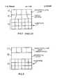
- FIG. 1is a diagram illustrating the prior art approach in which a monocrystalline layer is deposited by heteroepitaxy on a substrate which has not been lattice matched therewith;
- FIG. 2is a diagram showing the approach taken by the invention.
- the monocrystalline layer or film 22can thus be modified as described to form the mixed-crystal or compound.
- SIMOXseparation by implantation of oxygen.
- This commercially available substrateconsists of a silicon wafer having a buried amorphous silicon dioxide layer and a monocrystalline silicon surface layer.
- the monocrystalline silicon surface layeris initially thinned to a thickness of 20 nm by plasma etching.
- the substrate thus preparedis then heated at 850° C. (5 min.) in a molecular beam epitaxy (MBE) apparatus as is common in Si epitaxy to provide a perfect and clean surface.
- MBEmolecular beam epitaxy
- Si and Geare deposited in a ratio of 80:20 at 450° C. With subsequent annealing at 1100° C. for 30 seconds there is a complete homogenization of the Si seed layer and the deposited Si-Ge film.
- the resulting Si-Ge layercan be used directly for Si-Ge electrooptical devices or can serve as an intermediate layer (buffer layer) for further epitaxial growth of heterostructures and superlattices.
- the starting materialis again a silicon substrate with buried SiO 2 layer, namely, a SIMOX wafer.
- the monocrystalline Si surface layeris first chemically cleaned and then thinned to the desired thickness by plasma etching.
- Cois deposited. Silicide formation occurs during thermal treatment in the apparatus.
- the layer thicknessesdepend upon the materials used.
- CoSi 2resulted when a 100 nm Si starting layer was coated with 28 nm of a Co film after solid phase epitaxy with a silicide layer thickness of about 100 nm.
- For Complete reaction of the CoSi 2 layera temperature of 600° C. and 30 minutes was used.
- the resulting componenthad a monocrystalline silicide layer of especially high electrical and crystalline quality on an electrically insulating SiO 2 layer.
Landscapes
- Engineering & Computer Science (AREA)
- Physics & Mathematics (AREA)
- Condensed Matter Physics & Semiconductors (AREA)
- General Physics & Mathematics (AREA)
- Manufacturing & Machinery (AREA)
- Computer Hardware Design (AREA)
- Microelectronics & Electronic Packaging (AREA)
- Power Engineering (AREA)
- Chemical & Material Sciences (AREA)
- Materials Engineering (AREA)
- Recrystallisation Techniques (AREA)
- Crystals, And After-Treatments Of Crystals (AREA)
Abstract
Description
The present invention relates to a method of producing an article which can be used in the production of electronic, electrooptical or optical components and, especially, a crystalline structure or a structure provided with a crystalline film which can be used for electronic, electrooptical or optical circuit elements. Specifically the invention relates to a method of producing a structure having a single crystalline substrate with a buried amorphous layer and a single crystalline film deposited on this substrate.
The production of articles consisting of a crystalline substrate and a crystalline film on such substrate are known to be useful for the production of electronic, electrooptical and optical components.
The quality of the film which may be the active component of the article is affected by the structural match between substrate and film.
For example, if the lattice parameter of the applied layer is not matched to that of the substrate, lattice defects can develop at the interface in the newly formed layer and as this layer grows, these defects will propagate into the layer and can be detrimental to the electrical and especially the optical characteristics of the layer. Other approaches such as deposition upon porous silicon have not been successful in overcoming these problems.
it is, therefore, the principal object of the present invention to provide an improved method of forming a monocrystalline film of desired properties on a crystalline substrate whereby the formation of lattice defects at the interface of the substrate and the newly grown film can be avoided.
These objects are attained, in accordance with the invention by providing a buried amorphous layer on a crystalline substrate and upon this buried layer a monocrystalline layer. According to the invention the monocrystalline layer is transformed into a mixed-crystal structure or a chemical compound which either corresponds to the desired crystalline film or, in its lattice structure, comes closer to the desired crystalline film than the original monocrystalline film. More particularly, the method of making a crystalline element for an electronic, electrooptical or optical component comprises:
(a) providing a crystalline substrate having a buried amorphous layer formed therein and a monocrystalline layer on the amorphous layer and separated from the substrate by the amorphous layer; and
(b) transforming the monocrystalline layer into a mixed-crystal structure or a crystalline chemical compound.
In the transformation according to the invention of the monocrystalline surface layer into an alloy crystal (mixed crystal) or a crystalline chemical compound, the nonmatched crystal lattice of the surface layer is separated by the amorphous layer from the substrate and the propagation of defects from the interface is precluded as is the development of a defect network at the interface with the amorphous layer since there are no communicated stresses at the crystalline/amorphous interface.
The newly formed layer can itself be the desired product, i.e. the desired film for electrical, electronic, electrooptical or optical purposes, or can form a new base (buffer layer) for the growth of a further layer forming the desired film. In that case it constitutes a seed layer for the further monocrystalline growth of the desired film.
The transformation of the monocrystalline layer can be effected in various ways. It is, for example, possible to deposit the substances or components of the mixed-crystal or chemical compound upon the monocrystalline layer and simultaneously or subsequently to heat the layer to activate thermal diffusion and/or chemical reaction, achieving homogenization of the crystal layer or the formation of the mixed-crystal or the chemical compound.
Alternatively, the formation of the mixed-crystal or chemical compound can be attained by ion implantation in the monocrystalline layer, the ion implantation being followed by an annealing treatment. In the formation of the mixed-crystal (alloyed crystal) the concentrations of the components can be varied in the direction of growth whereby in a nonideal lattice matched system in the transformed layer, a gradient of the lattice parameter in the growth direction can result.
In a further alternative approach to transform the monocrystalline layer, the components required for formation of the mixed-crystal or the chemical compound can be deposited by epitaxy and, during or following the epitaxial deposition, an annealing treatment can be carried out.
It has been found that, with the present invention, the lattice parameters of the transformed layer can differ very significantly from that of the substrate material, but inspire of that, a substantially higher crystal quality of the transformed crystal layer can be obtained than with other approaches. This layer can have higher temperature resistance for example.
Through the use of a substrate with an electrically insulating buried amorphous layer, for example with SIMOX wafers the new film is dielectrically isolated from the substrate, the articles made in accordance with the invention have all of the inherent advantages of the SIMOX structure (isolation electronics) for microelectronic applications, for example high frequency properties.
The above and other objects, features and advantages of our invention will become more readily apparent from the following description, reference being made to the accompanying highly diagrammatic drawing in which:
FIG. 1 is a diagram illustrating the prior art approach in which a monocrystalline layer is deposited by heteroepitaxy on a substrate which has not been lattice matched therewith; and
FIG. 2 is a diagram showing the approach taken by the invention.
As can be seen from FIG. 1, it is not possible to grow a monocrystalline surface layer of unmatched lattice parameters onto the crystalline structure without the development of a defect network at theinterface 10 between the substrate 11 and themonocrystalline layer 12. In the diagrams of FIGS. 1 and 2 the difference in lattice parameters is represented by boxes of different sizes representing the crystalline cells.
By comparison, where anamorphous layer 20 is provided with thesubstrate 21 and themonocrystalline layer 22, the generation of a dislocation network is avoided.
The monocrystalline layer orfilm 22 can thus be modified as described to form the mixed-crystal or compound.
Monocrystalline Si-Ge mixed-crystal on SiO2 insulating layer.
The substrate is a SIMOX-wafer (SIMOX=separation by implantation of oxygen). This commercially available substrate consists of a silicon wafer having a buried amorphous silicon dioxide layer and a monocrystalline silicon surface layer.
The monocrystalline silicon surface layer is initially thinned to a thickness of 20 nm by plasma etching. The substrate thus prepared is then heated at 850° C. (5 min.) in a molecular beam epitaxy (MBE) apparatus as is common in Si epitaxy to provide a perfect and clean surface. Si and Ge are deposited in a ratio of 80:20 at 450° C. With subsequent annealing at 1100° C. for 30 seconds there is a complete homogenization of the Si seed layer and the deposited Si-Ge film. The resulting Si-Ge layer can be used directly for Si-Ge electrooptical devices or can serve as an intermediate layer (buffer layer) for further epitaxial growth of heterostructures and superlattices.
Monocrystalline cobalt silicide on silicon dioxide.
The starting material is again a silicon substrate with buried SiO2 layer, namely, a SIMOX wafer.
The monocrystalline Si surface layer is first chemically cleaned and then thinned to the desired thickness by plasma etching. In a vapor deposition apparatus under ultra high vacuum conditions, Co is deposited. Silicide formation occurs during thermal treatment in the apparatus. The layer thicknesses depend upon the materials used. CoSi2 resulted when a 100 nm Si starting layer was coated with 28 nm of a Co film after solid phase epitaxy with a silicide layer thickness of about 100 nm. For Complete reaction of the CoSi2 layer a temperature of 600° C. and 30 minutes was used. The resulting component had a monocrystalline silicide layer of especially high electrical and crystalline quality on an electrically insulating SiO2 layer.
Claims (11)
1. A method of making a crystalline element for an electronic, electrooptic or optical component, comprising:
(a) providing a crystalline substrate having a buried amorphous layer formed therein and a monocrystalline layer on said amorphous layer and separated from said substrate by said amorphous layer; and
(b) transforming said monocrystalline layer into a mixed-crystal structure or a crystalline chemical compound, whereby said amorphous layer is interposed between said substrate and said structure or compound and remains in the crystalline element of said component.
2. The method defined in claim 1 wherein the layer transformed in step (b) forms a desired crystalline film.
3. The method defined in claim 1 wherein the layer transformed in step (b) forms a crystalline film close in lattice structure to a desired crystalline film; said method further comprising the step of applying to the layer transformed in step (b) said desired crystalline film.
4. The method defined in claim 1 wherein the transforming of said monocrystalline layer in step (b) is effected by depositing at least one substance of said mixed-crystal structure or said crystalline chemical compound and applying heat to effect a thermal diffusion and/or a chemical reaction for homogenization of the resulting crystalline layer, the formation of the mixed-crystal structure or the formation of the compound.
5. The method defined in claim 4 wherein the heat is applied simultaneously with the deposition of said substance.
6. The method defined in claim 4 wherein the heat is applied subsequent to the deposition of said substance.
7. The method defined in claim 1 wherein the transformation in step (b) includes ion implantation in said monocrystalline layer.
8. The method defined in claim 7 further comprising annealing the monocrystalline layer after ion implantation.
9. The method defined in claim 1 wherein the formation of the mixed-crystal structure or said crystalline compound is effected by depositing a substance on said monocrystalline layer by epitaxy and, during or after the epitaxial deposition, said monocrystalline layer is subjected to an annealing heating.
10. The method defined in claim 1, further comprising the step of modifying a thickness of said monocrystalline layer prior to transformation in step (b).
11. The method defined in claim 10 wherein the modification of the thickness of said monocrystalline layer is effected by plasma etching.
Applications Claiming Priority (2)
| Application Number | Priority Date | Filing Date | Title |
|---|---|---|---|
| DE4029060.3 | 1990-09-13 | ||
| DE4029060ADE4029060C2 (en) | 1990-09-13 | 1990-09-13 | Process for the production of components for electronic, electro-optical and optical components |
Publications (1)
| Publication Number | Publication Date |
|---|---|
| US5735949Atrue US5735949A (en) | 1998-04-07 |
Family
ID=6414180
Family Applications (1)
| Application Number | Title | Priority Date | Filing Date |
|---|---|---|---|
| US07/759,571Expired - Fee RelatedUS5735949A (en) | 1990-09-13 | 1991-09-13 | Method of producing electronic, electrooptical and optical components |
Country Status (5)
| Country | Link |
|---|---|
| US (1) | US5735949A (en) |
| EP (1) | EP0475378B1 (en) |
| JP (1) | JPH076950A (en) |
| CA (1) | CA2051154C (en) |
| DE (1) | DE4029060C2 (en) |
Cited By (56)
| Publication number | Priority date | Publication date | Assignee | Title |
|---|---|---|---|---|
| US6184112B1 (en)* | 1998-12-02 | 2001-02-06 | Advanced Micro Devices, Inc. | Method of forming a MOSFET transistor with a shallow abrupt retrograde dopant profile |
| US6300147B1 (en)* | 1999-08-04 | 2001-10-09 | Mitsubishi Denki Kabushiki Kaisha | Method of inspecting semiconductor substrate |
| US6338756B2 (en) | 1998-06-30 | 2002-01-15 | Seh America, Inc. | In-situ post epitaxial treatment process |
| US6392257B1 (en) | 2000-02-10 | 2002-05-21 | Motorola Inc. | Semiconductor structure, semiconductor device, communicating device, integrated circuit, and process for fabricating the same |
| US6410941B1 (en) | 2000-06-30 | 2002-06-25 | Motorola, Inc. | Reconfigurable systems using hybrid integrated circuits with optical ports |
| US6427066B1 (en) | 2000-06-30 | 2002-07-30 | Motorola, Inc. | Apparatus and method for effecting communications among a plurality of remote stations |
| US6462360B1 (en) | 2001-08-06 | 2002-10-08 | Motorola, Inc. | Integrated gallium arsenide communications systems |
| US6464780B1 (en) | 1998-01-27 | 2002-10-15 | Forschungszentrum Julich Gmbh | Method for the production of a monocrystalline layer on a substrate with a non-adapted lattice and component containing one or several such layers |
| US6472694B1 (en) | 2001-07-23 | 2002-10-29 | Motorola, Inc. | Microprocessor structure having a compound semiconductor layer |
| US6477285B1 (en) | 2000-06-30 | 2002-11-05 | Motorola, Inc. | Integrated circuits with optical signal propagation |
| US6501973B1 (en) | 2000-06-30 | 2002-12-31 | Motorola, Inc. | Apparatus and method for measuring selected physical condition of an animate subject |
| WO2003010771A1 (en)* | 2001-07-23 | 2003-02-06 | Motorola, Inc. A Corporation Of The State Of Delaware | Memory system with independently accessible memory subsystems |
| US20030073293A1 (en)* | 1998-01-09 | 2003-04-17 | Armand Ferro | In situ growth of oxide and silicon layers |
| US6555946B1 (en) | 2000-07-24 | 2003-04-29 | Motorola, Inc. | Acoustic wave device and process for forming the same |
| US6563118B2 (en) | 2000-12-08 | 2003-05-13 | Motorola, Inc. | Pyroelectric device on a monocrystalline semiconductor substrate and process for fabricating same |
| US6562128B1 (en) | 2001-11-28 | 2003-05-13 | Seh America, Inc. | In-situ post epitaxial treatment process |
| US6583034B2 (en) | 2000-11-22 | 2003-06-24 | Motorola, Inc. | Semiconductor structure including a compliant substrate having a graded monocrystalline layer and methods for fabricating the structure and semiconductor devices including the structure |
| US6585424B2 (en) | 2001-07-25 | 2003-07-01 | Motorola, Inc. | Structure and method for fabricating an electro-rheological lens |
| US6589856B2 (en) | 2001-08-06 | 2003-07-08 | Motorola, Inc. | Method and apparatus for controlling anti-phase domains in semiconductor structures and devices |
| US6594414B2 (en) | 2001-07-25 | 2003-07-15 | Motorola, Inc. | Structure and method of fabrication for an optical switch |
| US20030172866A1 (en)* | 2002-03-13 | 2003-09-18 | Hsu Sheng Teng | Method for recrystallizing an amorphized silicon germanium film overlying silicon |
| US6639249B2 (en) | 2001-08-06 | 2003-10-28 | Motorola, Inc. | Structure and method for fabrication for a solid-state lighting device |
| US6638838B1 (en)* | 2000-10-02 | 2003-10-28 | Motorola, Inc. | Semiconductor structure including a partially annealed layer and method of forming the same |
| US6646293B2 (en) | 2001-07-18 | 2003-11-11 | Motorola, Inc. | Structure for fabricating high electron mobility transistors utilizing the formation of complaint substrates |
| US6667196B2 (en) | 2001-07-25 | 2003-12-23 | Motorola, Inc. | Method for real-time monitoring and controlling perovskite oxide film growth and semiconductor structure formed using the method |
| US6673667B2 (en) | 2001-08-15 | 2004-01-06 | Motorola, Inc. | Method for manufacturing a substantially integral monolithic apparatus including a plurality of semiconductor materials |
| US6673646B2 (en) | 2001-02-28 | 2004-01-06 | Motorola, Inc. | Growth of compound semiconductor structures on patterned oxide films and process for fabricating same |
| US6693298B2 (en) | 2001-07-20 | 2004-02-17 | Motorola, Inc. | Structure and method for fabricating epitaxial semiconductor on insulator (SOI) structures and devices utilizing the formation of a compliant substrate for materials used to form same |
| US6693033B2 (en) | 2000-02-10 | 2004-02-17 | Motorola, Inc. | Method of removing an amorphous oxide from a monocrystalline surface |
| US6703293B2 (en)* | 2002-07-11 | 2004-03-09 | Sharp Laboratories Of America, Inc. | Implantation at elevated temperatures for amorphization re-crystallization of Si1-xGex films on silicon substrates |
| US6709989B2 (en) | 2001-06-21 | 2004-03-23 | Motorola, Inc. | Method for fabricating a semiconductor structure including a metal oxide interface with silicon |
| US20040221792A1 (en)* | 2003-05-07 | 2004-11-11 | Micron Technology, Inc. | Strained Si/SiGe structures by ion implantation |
| US20040235264A1 (en)* | 2003-05-21 | 2004-11-25 | Micron Technology, Inc. | Gettering of silicon on insulator using relaxed silicon germanium epitaxial proximity layers |
| US20040232487A1 (en)* | 2003-05-21 | 2004-11-25 | Micron Technology, Inc. | Ultra-thin semiconductors bonded on glass substrates |
| US20040232422A1 (en)* | 2003-05-21 | 2004-11-25 | Micron Technology, Inc. | Wafer gettering using relaxed silicon germanium epitaxial proximity layers |
| US20050029619A1 (en)* | 2003-08-05 | 2005-02-10 | Micron Technology, Inc. | Strained Si/SiGe/SOI islands and processes of making same |
| US6855992B2 (en) | 2001-07-24 | 2005-02-15 | Motorola Inc. | Structure and method for fabricating configurable transistor devices utilizing the formation of a compliant substrate for materials used to form the same |
| US6885065B2 (en) | 2002-11-20 | 2005-04-26 | Freescale Semiconductor, Inc. | Ferromagnetic semiconductor structure and method for forming the same |
| US6916717B2 (en) | 2002-05-03 | 2005-07-12 | Motorola, Inc. | Method for growing a monocrystalline oxide layer and for fabricating a semiconductor device on a monocrystalline substrate |
| US20050217566A1 (en)* | 2002-04-24 | 2005-10-06 | Siegfried Mantl | Method for producing one or more monocrystalline layers, each with a different lattice structure, on one plane of a series of layers |
| US6965128B2 (en) | 2003-02-03 | 2005-11-15 | Freescale Semiconductor, Inc. | Structure and method for fabricating semiconductor microresonator devices |
| US20060001094A1 (en)* | 2003-05-21 | 2006-01-05 | Micron Technology, Inc. | Semiconductor on insulator structure |
| US6992321B2 (en) | 2001-07-13 | 2006-01-31 | Motorola, Inc. | Structure and method for fabricating semiconductor structures and devices utilizing piezoelectric materials |
| US7005717B2 (en) | 2000-05-31 | 2006-02-28 | Freescale Semiconductor, Inc. | Semiconductor device and method |
| US7019332B2 (en) | 2001-07-20 | 2006-03-28 | Freescale Semiconductor, Inc. | Fabrication of a wavelength locker within a semiconductor structure |
| US7020374B2 (en) | 2003-02-03 | 2006-03-28 | Freescale Semiconductor, Inc. | Optical waveguide structure and method for fabricating the same |
| US7045815B2 (en) | 2001-04-02 | 2006-05-16 | Freescale Semiconductor, Inc. | Semiconductor structure exhibiting reduced leakage current and method of fabricating same |
| US7046719B2 (en) | 2001-03-08 | 2006-05-16 | Motorola, Inc. | Soft handoff between cellular systems employing different encoding rates |
| US7105866B2 (en) | 2000-07-24 | 2006-09-12 | Freescale Semiconductor, Inc. | Heterojunction tunneling diodes and process for fabricating same |
| US7161227B2 (en) | 2001-08-14 | 2007-01-09 | Motorola, Inc. | Structure and method for fabricating semiconductor structures and devices for detecting an object |
| US7169619B2 (en) | 2002-11-19 | 2007-01-30 | Freescale Semiconductor, Inc. | Method for fabricating semiconductor structures on vicinal substrates using a low temperature, low pressure, alkaline earth metal-rich process |
| US7211852B2 (en) | 2001-01-19 | 2007-05-01 | Freescale Semiconductor, Inc. | Structure and method for fabricating GaN devices utilizing the formation of a compliant substrate |
| US7342276B2 (en) | 2001-10-17 | 2008-03-11 | Freescale Semiconductor, Inc. | Method and apparatus utilizing monocrystalline insulator |
| US20110204360A1 (en)* | 2007-11-16 | 2011-08-25 | Semiconductor Energy Laboratory Co., Ltd. | Photoelectric Conversion Device And Manufacturing Method Thereof |
| US20120049242A1 (en)* | 2009-04-21 | 2012-03-01 | The Silanna Group Pty Ltd | Optoelectronic device with lateral pin or pin junction |
| US8994009B2 (en) | 2011-09-07 | 2015-03-31 | Semiconductor Energy Laboratory Co., Ltd. | Photoelectric conversion device |
Citations (8)
| Publication number | Priority date | Publication date | Assignee | Title |
|---|---|---|---|---|
| US4177084A (en)* | 1978-06-09 | 1979-12-04 | Hewlett-Packard Company | Method for producing a low defect layer of silicon-on-sapphire wafer |
| US4425700A (en)* | 1980-08-13 | 1984-01-17 | Fujitsu Limited | Semiconductor device and method for manufacturing the same |
| US4463492A (en)* | 1981-09-30 | 1984-08-07 | Tokyo Shibaura Denki Kabushiki Kaisha | Method of forming a semiconductor device on insulating substrate by selective amorphosization followed by simultaneous activation and reconversion to single crystal state |
| US4902642A (en)* | 1987-08-07 | 1990-02-20 | Texas Instruments, Incorporated | Epitaxial process for silicon on insulator structure |
| JPH02237109A (en)* | 1989-03-10 | 1990-09-19 | Hitachi Cable Ltd | Manufacturing method of semiconductor device |
| US4975387A (en)* | 1989-12-15 | 1990-12-04 | The United States Of America As Represented By The Secretary Of The Navy | Formation of epitaxial si-ge heterostructures by solid phase epitaxy |
| JPH0311728A (en)* | 1989-06-09 | 1991-01-21 | Seiko Epson Corp | solid phase epitaxial |
| US5047111A (en)* | 1985-03-16 | 1991-09-10 | Director-General Of The Agency Of Industrial Science And Technology | Method of forming a metal silicide film |
Family Cites Families (3)
| Publication number | Priority date | Publication date | Assignee | Title |
|---|---|---|---|---|
| US4357183A (en)* | 1980-08-13 | 1982-11-02 | Massachusetts Institute Of Technology | Heteroepitaxy of germanium silicon on silicon utilizing alloying control |
| JPH0770711B2 (en)* | 1986-06-05 | 1995-07-31 | 株式会社日本自動車部品総合研究所 | Semiconductor device |
| DE3743734C2 (en)* | 1987-12-23 | 1996-09-26 | Licentia Gmbh | Process for producing buried, insulating layers and semiconductor bodies produced therewith |
- 1990
- 1990-09-13DEDE4029060Apatent/DE4029060C2/ennot_activeExpired - Fee Related
- 1991
- 1991-09-11EPEP91115340Apatent/EP0475378B1/ennot_activeExpired - Lifetime
- 1991-09-11CACA002051154Apatent/CA2051154C/ennot_activeExpired - Fee Related
- 1991-09-12JPJP3233480Apatent/JPH076950A/enactivePending
- 1991-09-13USUS07/759,571patent/US5735949A/ennot_activeExpired - Fee Related
Patent Citations (8)
| Publication number | Priority date | Publication date | Assignee | Title |
|---|---|---|---|---|
| US4177084A (en)* | 1978-06-09 | 1979-12-04 | Hewlett-Packard Company | Method for producing a low defect layer of silicon-on-sapphire wafer |
| US4425700A (en)* | 1980-08-13 | 1984-01-17 | Fujitsu Limited | Semiconductor device and method for manufacturing the same |
| US4463492A (en)* | 1981-09-30 | 1984-08-07 | Tokyo Shibaura Denki Kabushiki Kaisha | Method of forming a semiconductor device on insulating substrate by selective amorphosization followed by simultaneous activation and reconversion to single crystal state |
| US5047111A (en)* | 1985-03-16 | 1991-09-10 | Director-General Of The Agency Of Industrial Science And Technology | Method of forming a metal silicide film |
| US4902642A (en)* | 1987-08-07 | 1990-02-20 | Texas Instruments, Incorporated | Epitaxial process for silicon on insulator structure |
| JPH02237109A (en)* | 1989-03-10 | 1990-09-19 | Hitachi Cable Ltd | Manufacturing method of semiconductor device |
| JPH0311728A (en)* | 1989-06-09 | 1991-01-21 | Seiko Epson Corp | solid phase epitaxial |
| US4975387A (en)* | 1989-12-15 | 1990-12-04 | The United States Of America As Represented By The Secretary Of The Navy | Formation of epitaxial si-ge heterostructures by solid phase epitaxy |
Cited By (85)
| Publication number | Priority date | Publication date | Assignee | Title |
|---|---|---|---|---|
| US7105055B2 (en) | 1998-01-09 | 2006-09-12 | Asm America, Inc. | In situ growth of oxide and silicon layers |
| US20040206297A1 (en)* | 1998-01-09 | 2004-10-21 | Armand Ferro | In situ growth of oxide and silicon layers |
| US20030073293A1 (en)* | 1998-01-09 | 2003-04-17 | Armand Ferro | In situ growth of oxide and silicon layers |
| US7112538B2 (en) | 1998-01-09 | 2006-09-26 | Asm America, Inc. | In situ growth of oxide and silicon layers |
| US20050205010A1 (en)* | 1998-01-09 | 2005-09-22 | Armand Ferro | In situ growth of oxide and silicon layers |
| US6749687B1 (en) | 1998-01-09 | 2004-06-15 | Asm America, Inc. | In situ growth of oxide and silicon layers |
| US8317921B2 (en) | 1998-01-09 | 2012-11-27 | Asm America, Inc. | In situ growth of oxide and silicon layers |
| US6464780B1 (en) | 1998-01-27 | 2002-10-15 | Forschungszentrum Julich Gmbh | Method for the production of a monocrystalline layer on a substrate with a non-adapted lattice and component containing one or several such layers |
| US6471771B2 (en) | 1998-06-30 | 2002-10-29 | Seh America, Inc. | In-situ post epitaxial treatment process |
| US20030159649A1 (en)* | 1998-06-30 | 2003-08-28 | Dietze Gerald R. | In-situ post epitaxial treatment process |
| US6808564B2 (en) | 1998-06-30 | 2004-10-26 | Seh America, Inc. | In-situ post epitaxial treatment process |
| US6338756B2 (en) | 1998-06-30 | 2002-01-15 | Seh America, Inc. | In-situ post epitaxial treatment process |
| US6184112B1 (en)* | 1998-12-02 | 2001-02-06 | Advanced Micro Devices, Inc. | Method of forming a MOSFET transistor with a shallow abrupt retrograde dopant profile |
| US6300147B1 (en)* | 1999-08-04 | 2001-10-09 | Mitsubishi Denki Kabushiki Kaisha | Method of inspecting semiconductor substrate |
| US7067856B2 (en) | 2000-02-10 | 2006-06-27 | Freescale Semiconductor, Inc. | Semiconductor structure, semiconductor device, communicating device, integrated circuit, and process for fabricating the same |
| US6693033B2 (en) | 2000-02-10 | 2004-02-17 | Motorola, Inc. | Method of removing an amorphous oxide from a monocrystalline surface |
| US6392257B1 (en) | 2000-02-10 | 2002-05-21 | Motorola Inc. | Semiconductor structure, semiconductor device, communicating device, integrated circuit, and process for fabricating the same |
| US7005717B2 (en) | 2000-05-31 | 2006-02-28 | Freescale Semiconductor, Inc. | Semiconductor device and method |
| US6501973B1 (en) | 2000-06-30 | 2002-12-31 | Motorola, Inc. | Apparatus and method for measuring selected physical condition of an animate subject |
| US6477285B1 (en) | 2000-06-30 | 2002-11-05 | Motorola, Inc. | Integrated circuits with optical signal propagation |
| US6427066B1 (en) | 2000-06-30 | 2002-07-30 | Motorola, Inc. | Apparatus and method for effecting communications among a plurality of remote stations |
| US6410941B1 (en) | 2000-06-30 | 2002-06-25 | Motorola, Inc. | Reconfigurable systems using hybrid integrated circuits with optical ports |
| US6555946B1 (en) | 2000-07-24 | 2003-04-29 | Motorola, Inc. | Acoustic wave device and process for forming the same |
| US7105866B2 (en) | 2000-07-24 | 2006-09-12 | Freescale Semiconductor, Inc. | Heterojunction tunneling diodes and process for fabricating same |
| US6638838B1 (en)* | 2000-10-02 | 2003-10-28 | Motorola, Inc. | Semiconductor structure including a partially annealed layer and method of forming the same |
| US6583034B2 (en) | 2000-11-22 | 2003-06-24 | Motorola, Inc. | Semiconductor structure including a compliant substrate having a graded monocrystalline layer and methods for fabricating the structure and semiconductor devices including the structure |
| US6563118B2 (en) | 2000-12-08 | 2003-05-13 | Motorola, Inc. | Pyroelectric device on a monocrystalline semiconductor substrate and process for fabricating same |
| US7211852B2 (en) | 2001-01-19 | 2007-05-01 | Freescale Semiconductor, Inc. | Structure and method for fabricating GaN devices utilizing the formation of a compliant substrate |
| US6673646B2 (en) | 2001-02-28 | 2004-01-06 | Motorola, Inc. | Growth of compound semiconductor structures on patterned oxide films and process for fabricating same |
| US7046719B2 (en) | 2001-03-08 | 2006-05-16 | Motorola, Inc. | Soft handoff between cellular systems employing different encoding rates |
| US7045815B2 (en) | 2001-04-02 | 2006-05-16 | Freescale Semiconductor, Inc. | Semiconductor structure exhibiting reduced leakage current and method of fabricating same |
| US6709989B2 (en) | 2001-06-21 | 2004-03-23 | Motorola, Inc. | Method for fabricating a semiconductor structure including a metal oxide interface with silicon |
| US6992321B2 (en) | 2001-07-13 | 2006-01-31 | Motorola, Inc. | Structure and method for fabricating semiconductor structures and devices utilizing piezoelectric materials |
| US6646293B2 (en) | 2001-07-18 | 2003-11-11 | Motorola, Inc. | Structure for fabricating high electron mobility transistors utilizing the formation of complaint substrates |
| US6693298B2 (en) | 2001-07-20 | 2004-02-17 | Motorola, Inc. | Structure and method for fabricating epitaxial semiconductor on insulator (SOI) structures and devices utilizing the formation of a compliant substrate for materials used to form same |
| US7019332B2 (en) | 2001-07-20 | 2006-03-28 | Freescale Semiconductor, Inc. | Fabrication of a wavelength locker within a semiconductor structure |
| US6472694B1 (en) | 2001-07-23 | 2002-10-29 | Motorola, Inc. | Microprocessor structure having a compound semiconductor layer |
| WO2003010771A1 (en)* | 2001-07-23 | 2003-02-06 | Motorola, Inc. A Corporation Of The State Of Delaware | Memory system with independently accessible memory subsystems |
| US6855992B2 (en) | 2001-07-24 | 2005-02-15 | Motorola Inc. | Structure and method for fabricating configurable transistor devices utilizing the formation of a compliant substrate for materials used to form the same |
| US6594414B2 (en) | 2001-07-25 | 2003-07-15 | Motorola, Inc. | Structure and method of fabrication for an optical switch |
| US6667196B2 (en) | 2001-07-25 | 2003-12-23 | Motorola, Inc. | Method for real-time monitoring and controlling perovskite oxide film growth and semiconductor structure formed using the method |
| US6585424B2 (en) | 2001-07-25 | 2003-07-01 | Motorola, Inc. | Structure and method for fabricating an electro-rheological lens |
| US6589856B2 (en) | 2001-08-06 | 2003-07-08 | Motorola, Inc. | Method and apparatus for controlling anti-phase domains in semiconductor structures and devices |
| US6639249B2 (en) | 2001-08-06 | 2003-10-28 | Motorola, Inc. | Structure and method for fabrication for a solid-state lighting device |
| US6462360B1 (en) | 2001-08-06 | 2002-10-08 | Motorola, Inc. | Integrated gallium arsenide communications systems |
| US7161227B2 (en) | 2001-08-14 | 2007-01-09 | Motorola, Inc. | Structure and method for fabricating semiconductor structures and devices for detecting an object |
| US6673667B2 (en) | 2001-08-15 | 2004-01-06 | Motorola, Inc. | Method for manufacturing a substantially integral monolithic apparatus including a plurality of semiconductor materials |
| US7342276B2 (en) | 2001-10-17 | 2008-03-11 | Freescale Semiconductor, Inc. | Method and apparatus utilizing monocrystalline insulator |
| US6562128B1 (en) | 2001-11-28 | 2003-05-13 | Seh America, Inc. | In-situ post epitaxial treatment process |
| US20030172866A1 (en)* | 2002-03-13 | 2003-09-18 | Hsu Sheng Teng | Method for recrystallizing an amorphized silicon germanium film overlying silicon |
| US6793731B2 (en)* | 2002-03-13 | 2004-09-21 | Sharp Laboratories Of America, Inc. | Method for recrystallizing an amorphized silicon germanium film overlying silicon |
| US20050217566A1 (en)* | 2002-04-24 | 2005-10-06 | Siegfried Mantl | Method for producing one or more monocrystalline layers, each with a different lattice structure, on one plane of a series of layers |
| US6916717B2 (en) | 2002-05-03 | 2005-07-12 | Motorola, Inc. | Method for growing a monocrystalline oxide layer and for fabricating a semiconductor device on a monocrystalline substrate |
| US6703293B2 (en)* | 2002-07-11 | 2004-03-09 | Sharp Laboratories Of America, Inc. | Implantation at elevated temperatures for amorphization re-crystallization of Si1-xGex films on silicon substrates |
| US7169619B2 (en) | 2002-11-19 | 2007-01-30 | Freescale Semiconductor, Inc. | Method for fabricating semiconductor structures on vicinal substrates using a low temperature, low pressure, alkaline earth metal-rich process |
| US6885065B2 (en) | 2002-11-20 | 2005-04-26 | Freescale Semiconductor, Inc. | Ferromagnetic semiconductor structure and method for forming the same |
| US7020374B2 (en) | 2003-02-03 | 2006-03-28 | Freescale Semiconductor, Inc. | Optical waveguide structure and method for fabricating the same |
| US6965128B2 (en) | 2003-02-03 | 2005-11-15 | Freescale Semiconductor, Inc. | Structure and method for fabricating semiconductor microresonator devices |
| US6987037B2 (en)* | 2003-05-07 | 2006-01-17 | Micron Technology, Inc. | Strained Si/SiGe structures by ion implantation |
| US20050285139A1 (en)* | 2003-05-07 | 2005-12-29 | Micron Technology, Inc. | Strained Si/SiGe structures by ion implantation |
| US20040221792A1 (en)* | 2003-05-07 | 2004-11-11 | Micron Technology, Inc. | Strained Si/SiGe structures by ion implantation |
| US7394111B2 (en) | 2003-05-07 | 2008-07-01 | Micron Technology, Inc. | Strained Si/SiGe structures by ion implantation |
| US20050023612A1 (en)* | 2003-05-21 | 2005-02-03 | Micron Technology, Inc. | Ultra-thin semiconductors bonded on glass substrates |
| US7687329B2 (en) | 2003-05-21 | 2010-03-30 | Micron Technology, Inc. | Gettering of silicon on insulator using relaxed silicon germanium epitaxial proximity layers |
| US20060263994A1 (en)* | 2003-05-21 | 2006-11-23 | Micron Technology, Inc. | Semiconductors bonded on glass substrates |
| US20040235264A1 (en)* | 2003-05-21 | 2004-11-25 | Micron Technology, Inc. | Gettering of silicon on insulator using relaxed silicon germanium epitaxial proximity layers |
| US20060001094A1 (en)* | 2003-05-21 | 2006-01-05 | Micron Technology, Inc. | Semiconductor on insulator structure |
| US20060258063A1 (en)* | 2003-05-21 | 2006-11-16 | Micron Technology, Inc. | Gettering of silicon on insulator using relaxed silicon germanium epitaxial proximity layers |
| US7662701B2 (en) | 2003-05-21 | 2010-02-16 | Micron Technology, Inc. | Gettering of silicon on insulator using relaxed silicon germanium epitaxial proximity layers |
| US7528463B2 (en) | 2003-05-21 | 2009-05-05 | Micron Technolgy, Inc. | Semiconductor on insulator structure |
| US7271445B2 (en) | 2003-05-21 | 2007-09-18 | Micron Technology, Inc. | Ultra-thin semiconductors bonded on glass substrates |
| US7273788B2 (en) | 2003-05-21 | 2007-09-25 | Micron Technology, Inc. | Ultra-thin semiconductors bonded on glass substrates |
| US20040232422A1 (en)* | 2003-05-21 | 2004-11-25 | Micron Technology, Inc. | Wafer gettering using relaxed silicon germanium epitaxial proximity layers |
| US20040232487A1 (en)* | 2003-05-21 | 2004-11-25 | Micron Technology, Inc. | Ultra-thin semiconductors bonded on glass substrates |
| US7501329B2 (en) | 2003-05-21 | 2009-03-10 | Micron Technology, Inc. | Wafer gettering using relaxed silicon germanium epitaxial proximity layers |
| US7504310B2 (en) | 2003-05-21 | 2009-03-17 | Micron Technology, Inc. | Semiconductors bonded on glass substrates |
| US7262428B2 (en) | 2003-08-05 | 2007-08-28 | Micron Technology, Inc. | Strained Si/SiGe/SOI islands and processes of making same |
| US20050029619A1 (en)* | 2003-08-05 | 2005-02-10 | Micron Technology, Inc. | Strained Si/SiGe/SOI islands and processes of making same |
| US20050087842A1 (en)* | 2003-08-05 | 2005-04-28 | Micron Technology, Inc. | Strained Si/SiGe/SOI islands and processes of making same |
| US7153753B2 (en) | 2003-08-05 | 2006-12-26 | Micron Technology, Inc. | Strained Si/SiGe/SOI islands and processes of making same |
| US20110204360A1 (en)* | 2007-11-16 | 2011-08-25 | Semiconductor Energy Laboratory Co., Ltd. | Photoelectric Conversion Device And Manufacturing Method Thereof |
| US8093590B2 (en)* | 2007-11-16 | 2012-01-10 | Semiconductor Energy Laboratory Co., Ltd. | Photoelectric conversion device |
| US20120049242A1 (en)* | 2009-04-21 | 2012-03-01 | The Silanna Group Pty Ltd | Optoelectronic device with lateral pin or pin junction |
| US8962376B2 (en)* | 2009-04-21 | 2015-02-24 | The Silanna Group Pty Ltd | Optoelectronic device with lateral pin or pin junction |
| US8994009B2 (en) | 2011-09-07 | 2015-03-31 | Semiconductor Energy Laboratory Co., Ltd. | Photoelectric conversion device |
Also Published As
| Publication number | Publication date |
|---|---|
| EP0475378B1 (en) | 1998-01-07 |
| CA2051154C (en) | 2000-12-12 |
| EP0475378A1 (en) | 1992-03-18 |
| JPH076950A (en) | 1995-01-10 |
| DE4029060A1 (en) | 1992-03-19 |
| DE4029060C2 (en) | 1994-01-13 |
| CA2051154A1 (en) | 1992-03-14 |
Similar Documents
| Publication | Publication Date | Title |
|---|---|---|
| US5735949A (en) | Method of producing electronic, electrooptical and optical components | |
| EP0331467B1 (en) | Method of forming semiconductor thin film | |
| US11699615B2 (en) | High resistivity semiconductor-on-insulator wafer and a method of manufacture | |
| US5019529A (en) | Heteroepitaxial growth method | |
| US6030884A (en) | Method of bonding a III-V group compound semiconductor layer on a silicon substrate | |
| JP5254195B2 (en) | Method for manufacturing a single crystal semiconductor layer over a substrate | |
| US20080146008A1 (en) | Ultra-Thin High-Quality Germanium on Silicon By Low-Temperature Epitaxy and Insulator-Capped Annealing | |
| US5363793A (en) | Method for forming crystals | |
| JP3007971B1 (en) | Method of forming single crystal thin film | |
| JPH04233219A (en) | Method for manufacturing products consisting of semiconductor devices | |
| US5066355A (en) | Method of producing hetero structure | |
| US5281551A (en) | Method for delta-doping in GaAs epitaxial layer grown on silicon substrate by metalorganic chemical vapor deposition | |
| JPS62132312A (en) | Manufacture of semiconductor thin film | |
| US20240258155A1 (en) | Methods of manufacturing semiconductor-on-insulator wafers having charge trapping layers with controlled stress | |
| JP2651146B2 (en) | Crystal manufacturing method | |
| Grundmann et al. | Antiphase-domain-free InP on Si (001): Optimization of MOCVD process | |
| JP2659745B2 (en) | III-Group V compound crystal article and method of forming the same | |
| JPS6191917A (en) | Manufacture of semiconductor thin film crystal | |
| JP2592832B2 (en) | Crystal formation method | |
| EP0289117B1 (en) | Method of forming crystals on a substrate | |
| JP2599576B2 (en) | Method for growing two-dimensional thin film of group III-V compound semiconductor | |
| JPH01723A (en) | 3-Group V compound crystal article and method for forming the same | |
| JP3352196B2 (en) | Method of manufacturing bonded substrate and method of manufacturing semiconductor substrate | |
| JPH0216720A (en) | Solid phase epitaxy method | |
| JPS6229397B2 (en) |
Legal Events
| Date | Code | Title | Description |
|---|---|---|---|
| AS | Assignment | Owner name:FORSCHUNGSZENTRUM JULICH GMBH, GERMANY Free format text:ASSIGNMENT OF ASSIGNORS INTEREST.;ASSIGNORS:MANTL, SIEGFRIED;HOLLANDER, BERND;BUTZ, RAINER;REEL/FRAME:005888/0737 Effective date:19911009 | |
| FEPP | Fee payment procedure | Free format text:PAYOR NUMBER ASSIGNED (ORIGINAL EVENT CODE: ASPN); ENTITY STATUS OF PATENT OWNER: LARGE ENTITY | |
| REMI | Maintenance fee reminder mailed | ||
| LAPS | Lapse for failure to pay maintenance fees | ||
| STCH | Information on status: patent discontinuation | Free format text:PATENT EXPIRED DUE TO NONPAYMENT OF MAINTENANCE FEES UNDER 37 CFR 1.362 | |
| FP | Lapsed due to failure to pay maintenance fee | Effective date:20020407 |