US5732111A - Frequency error compensation for direct sequence spread spectrum systems - Google Patents
Frequency error compensation for direct sequence spread spectrum systemsDownload PDFInfo
- Publication number
- US5732111A US5732111AUS08/568,095US56809595AUS5732111AUS 5732111 AUS5732111 AUS 5732111AUS 56809595 AUS56809595 AUS 56809595AUS 5732111 AUS5732111 AUS 5732111A
- Authority
- US
- United States
- Prior art keywords
- value
- phase
- cross product
- bit
- signals
- Prior art date
- Legal status (The legal status is an assumption and is not a legal conclusion. Google has not performed a legal analysis and makes no representation as to the accuracy of the status listed.)
- Expired - Lifetime
Links
Images


Classifications
- H—ELECTRICITY
- H04—ELECTRIC COMMUNICATION TECHNIQUE
- H04L—TRANSMISSION OF DIGITAL INFORMATION, e.g. TELEGRAPHIC COMMUNICATION
- H04L27/00—Modulated-carrier systems
- H04L27/18—Phase-modulated carrier systems, i.e. using phase-shift keying
- H04L27/22—Demodulator circuits; Receiver circuits
- H04L27/233—Demodulator circuits; Receiver circuits using non-coherent demodulation
- H04L27/2332—Demodulator circuits; Receiver circuits using non-coherent demodulation using a non-coherent carrier
- H—ELECTRICITY
- H04—ELECTRIC COMMUNICATION TECHNIQUE
- H04L—TRANSMISSION OF DIGITAL INFORMATION, e.g. TELEGRAPHIC COMMUNICATION
- H04L1/00—Arrangements for detecting or preventing errors in the information received
- H04L1/20—Arrangements for detecting or preventing errors in the information received using signal quality detector
- H—ELECTRICITY
- H04—ELECTRIC COMMUNICATION TECHNIQUE
- H04L—TRANSMISSION OF DIGITAL INFORMATION, e.g. TELEGRAPHIC COMMUNICATION
- H04L27/00—Modulated-carrier systems
- H04L27/0014—Carrier regulation
- H04L2027/0024—Carrier regulation at the receiver end
- H04L2027/0026—Correction of carrier offset
- H04L2027/003—Correction of carrier offset at baseband only
- H—ELECTRICITY
- H04—ELECTRIC COMMUNICATION TECHNIQUE
- H04L—TRANSMISSION OF DIGITAL INFORMATION, e.g. TELEGRAPHIC COMMUNICATION
- H04L27/00—Modulated-carrier systems
- H04L27/0014—Carrier regulation
- H04L2027/0044—Control loops for carrier regulation
- H04L2027/0053—Closed loops
- H04L2027/0057—Closed loops quadrature phase
- H—ELECTRICITY
- H04—ELECTRIC COMMUNICATION TECHNIQUE
- H04L—TRANSMISSION OF DIGITAL INFORMATION, e.g. TELEGRAPHIC COMMUNICATION
- H04L27/00—Modulated-carrier systems
- H04L27/0014—Carrier regulation
- H04L2027/0083—Signalling arrangements
- H04L2027/0089—In-band signals
- H04L2027/0093—Intermittant signals
- H04L2027/0095—Intermittant signals in a preamble or similar structure
Definitions
- the present inventionrelates generally to improvements in digital spread spectrum systems and, more particularly, pertains to a new and improved device and method for frequency calibration, estimation and compensation for digital cordless direct sequence spread spectrum telephones.
- Cordless telephonescurrently exist which provide good speech quality using analog frequency modulation in the 46/49 MHz band. These analog cordless phones are inexpensive and have become a common replacement for the traditional corded phones. However, analog cordless phones have a limited useful range, requiring the handset to be operated in close proximity to the base station. Also, analog cordless phones are susceptible to interference and lack adequate security for protecting the privacy of conversations.
- Digital modulation and codingoffer more robust voice communication over a radio channel than analog modulation. Digital modulation also provides a more noise-free conversation by suppressing co-channel and adjacent channel interference. Additionally, with digital modulation and coding, effective scrambling codes can be added to improve phone security.
- Another solutionis to use the 902-928 MHz Industrial, Medical and Scientific (ISM) band for radio transmission and reception.
- ISMIndustrial, Medical and Scientific
- the Federal Communications Commission (FCC)allows transmitters in this band to have increased power levels, as compared to the 46/49 MHz band, which increases the useful operating range.
- the FCCrequires that the phone systems implement spread spectrum modulation.
- DSSSDirect Sequence Spread Spectrum
- Initial frequency calibration between the handset and the baseoccurs when the handset is parked in the base station cradle. Both the handset and the base station transmit and receive using a frequency offset bin as an estimate of the frequency error.
- the allowable frequency rangeis divided into several bins and a signal quality value is calculated based on the dot product detector and signal quality hardware for each bin.
- the Numerically Controlled Oscillator (NCO) on each sideis then set to the frequency bin which resulted in the maximum signal quality.
- a communication linkis then established between the base and handset to allow Automatic Frequency Control (AFC) tracking to adjust the NCO.
- AFCAutomatic Frequency Control
- the frequency error estimation during AFCis performed by cross product demodulation of the I and Q signals, with the output of the cross product detector limited to one bit.
- the cross product outputis then filtered by a random walk digital filter which smoothes amplitude errors in the frequency estimation.
- Frequency compensationis performed by a complex phase rotator and a Numerically Controlled Oscillator (NCO).
- the phase rotatorperforms complex rotations on the I and Q signals to offset the actual frequency error.
- the AFC compensationincreases or decreases the frequency error by adjusting the value of the phase rotator's NCO, which adjusts the phase of the incoming signal.
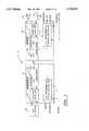
- FIG. 1is a system-level diagram of a base station and a handset that collectively form a digital cordless telephone of the present invention
- FIG. 2is a functional block diagram of the RF Modem, Baseband Modem, Audio Modem, and Controller of the handset, the functional blocks of the base station being identical;
- FIG. 3is a block diagram of part of the Baseband Modem showing more detail than FIG. 2;
- FIG. 4is a block diagram of a preferred embodiment of the Phase Rotator block shown in FIG. 3;
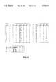
- FIG. 5is a table showing the conversion mapping for converting I and Q signals from rectangular to polar form
- FIG. 6is a table showing the conversion mapping for converting Magnitude and Phase signals from polar to rectangular form
- FIG. 7is a block diagram of a preferred embodiment of the Matched Filter blocks shown in FIG. 3;
- FIG. 8is a graph showing a preferred frequency division for the frequency bins used by the calibration procedure.
- FIG. 9shows the transmission and reception of A-frames and V-frames for 20 frequency bins
- FIG. 10shows the structures for two types of data flames used in a preferred embodiment, an acquisition frame (A-frame) and a voice frame (V-frame);
- A-frameacquisition frame
- V-framevoice frame
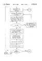
- FIG. 11is a flowchart of the frequency calibration method used when the handset is physically in the cradle of the base station.
- FIG. 12is a block diagram showing in greater detail the Frequency Error Estimate block of FIG. 3;
- FIG. 13is a block diagram showing the preferred embodiment of the Accumulator blocks shown in FIG. 12;
- FIG. 14shows the limited output values for the Cross Product used in the AFC circuits.
- a digital cordless telephone (DCT) 10comprises a base station 20 and at least one handset 30.
- the DCT 10is designed to provide full duplex voice communication between the handset 30 and the public switched telephone network (PSTN) (not shown) by way of an RF link through the base station 20.
- PSTNpublic switched telephone network
- the base station 20 and the handset 30both include a Radio Modem 28, 38, respectively, which are composed of a Radio Frequency (RF) Modem 25, 35 and a Baseband Modem 26, 36, respectively.
- the RF Modems 25, 35transmit digital voice and control data between the base station 20 and the handset 30.
- the base station 20 and handset 30also have Audio Modems 21, 31 that respectively provide voice transport between the base station 20 and the PSTN and between the handset 30 and a microphone 32 and a speaker 33.
- the base station 20 and the handset 30both have a system controller 27, 37, respectively, for call processing and control functions.
- the controllers 27, 37function to provide the protocol for the Radio Modems 28, 38 to allow link establishment, maintenance, and power management.
- the preferred RF Modem 35is a direct conversion transceiver.
- analog wave-shaped baseband data (TXD)is modulated directly to the carrier frequency.
- the carrieris directly converted to analog baseband in-phase (RXI) and quadrature (RXQ) signals.
- the preferred DCT 10uses frequency division multiple access (FDMA) channelization which, in the 26 MHz-wide ISM band, provides 21 frequency channels at 1.2 MHz channel spacing.
- FDMAfrequency division multiple access
- the preferred Baseband Modem 36is a narrow-band direct sequence spread spectrum (DSSS) burst modem that supports FDMA channelization and time division duplexing (TDD).
- the preferred transmit and receive time slotsare both 2 ms wide, providing a 4 ms Tx/Rx superframe.
- the preferred modulation for datais differentially encoded Binary Phase Shift Keying (BPSK), and for the spreading code is BPSK.
- BPSKBinary Phase Shift Keying
- the differential encoding of the datais done such that a change of polarity over a bit interval represents a "-1" and a continuity of polarity represents a "+1.”
- the DCT 10preferably uses bipolar signalling where +1 volt signal represents a binary "1" and a -1 volt signal represents a binary "0".
- Each bitis preferably direct sequence spread spectrum modulated with a 12-chip spreading code.
- the preferred spreading coderepeats on bit boundaries so that, it remains “as is” when multiplied by a binary "1” (+1 volt) and is inverted when multiplied by a binary "0" (-1 volt).
- the preferred bit rateis 80 kHz, whereby the chip rate for the preferred 12-chip spreading code is 960 kHz (12 ⁇ 80 kHz).
- FIG. 10shows the preferred 160-bit frame structures for a voice frame (V-frame) and an acquisition frame (A-frame).
- V-framevoice frame
- A-frameacquisition frame
- the "Db" bit (24)is always "+1" to provide an initial phase reference for decoding the differentially encoded data during reception.
- the first 23 bits(1-23) are all DC settle bits (all “1”s), which allow for DC settling of bias circuits in the RF Modem 35.
- the next 100 bits (24-123)are dotting bits (1,0, 1,0, . . . repeated), used by the Baseband Modem 36 for timing acquisition and tracking during an initial reception.
- the next 32 bits (124-155)are an ID word, followed by an "L-bit” (156) which is used to request an RF link response.
- guard bits(157-160), which account for radio propagation and circuit delays.
- the preferred RF Modem 35is shown to have a lower transmit path and an upper receive path.
- a common frequency synthesizer 353provides the local oscillator frequency needed for modulation and demodulation.
- the RF Modem 35receives digital spread spectrum data TXD from the Baseband Modem 36, and passes the data TXD through a pair of filters 351,352 to a modulator 354 where it directly modulates the RF carrier.
- the first filter 351is preferably a 10 kHz high pass filter 351 for removing any DC contributed by bias networks and the second filter 352 is preferably a 650 kHz low-pass filter for spectral shaping.
- the modulated signalis then amplified using a variable output amplifier 356 and routed to a Transmit/Receive (T/R) switch 357 for transmission by an antenna 358.
- T/R switch 357selects the receive path from the antenna 358, filters the received signal through a band-pass filter 359 to reject out-of-band signals, and then amplifies the filtered signal with a low noise amplifier 340.
- the signalthen enters a pair of mixers 341(I), 341(Q) that down-convert it to analog in-phase (RXI) and quadrature (RXQ) spread spectrum signals.
- each spread spectrum signal RXI, RXQis then passed through a pair of high-pass/low-pass filter blocks 342(I), 342(Q), respectively, to provide FDMA channel selectivity. Finally, each spread spectrum signal RXI, RXQ is amplified with programmable gain amplifiers 343(I), 343(Q) to bring the signal up to proper voltage levels.
- the Baseband Modem 36is shown to have a transmitter block 361 and a pair of Analog-to-Digital Converters (ADCs) 362(I), 362(Q) that feed a receiver block 364.
- ADCsAnalog-to-Digital Converters
- the transmitter block 361takes analog baseband data from the Audio Modem 31, digitizes it, differentially encodes it, combines it with a spreading code, and then provides the resulting digital spread spectrum data TXD to the RF Modem 35 where it directly modulates the carrier for transmission.
- the ADCs 362(I), 362(Q)convert the RF Modem's analog spread spectrum signals RXI, RXQ into digital spread spectrum data I, Q.
- the receiver block 364receives the digital spread spectrum data I, Q. It then removes the spreading code to recover the digital baseband data, decodes the differentially encoded data, and provides the resulting digital baseband data to the Audio Modem 31 for acoustic reproduction on the speaker 33.
- FIG. 3shows the major functional blocks of the Baseband Modem 36 in further detail.
- the in-phase and quadrature analog signals RXI 40, RXQ 42are provided to the ADCs 362(I), 362(Q) for conversion to corresponding digital signals I, Q.
- the preferred ADCs 362(I), 362(Q)sample the analog baseband signals RXI 40, RXQ 42 at 1.92 MHz (2 times the chip rate) and convert such analog signals into a series of 4-bit, 2's complement, digital signals I, Q.
- the ADCspreferably implement the following quantization values to reduce the data-movement requirements (ensuring the least significant bit (LSB) is always "1" so it may be implied) and to simplify later multiplication of the digital spread spectrum signals I, Q by ⁇ 1 (requiring only a simple inversion of the most significant three bits):
- the digitized RXI 40 and RXQ 42 signalsare then multiplied by (cos( ⁇ (t)+jsin( ⁇ (t))) by the Phase Rotator 48, FIG. 4, where ⁇ (t) represents the phase value supplied by the Numerically Controlled Oscillator (NCO) 68. If "PhaseRotatorNCO" equals ⁇ (t), this function may be represented as:
- the Phase Rotator 48performs this function by first converting the digitized RXI 40 and RXQ 42 signals from rectangular to polar form by the Rectangular to Polar converter 84 form as shown in FIG. 4.
- the I In 80 and Q In 82 signals(corresponding to digitized RXI 40 and RXQ 42, respectively) are represented with three Magnitude bits 86 and six Phase bits 88 which are determined by converting the six input bits into nine output bits as shown in FIG. 5.
- Small input signalsare revectored to a minimum amplitude during the Phase Rotator 48 calculations to reduce quantization noise of the output phase, thus improving performance.
- the Original Phase 88 component of the I In 80 and Q In 82 signalsis modified by the six MSBs from the NCO Accumulator 68.
- the Six-Bit Adder 90adds the Original Phase 88 with the six MSBs of the NCO 68 value and outputs a Modified Phase 100.
- the Magnitude 86 and Modified Phase 100 bitsare then converted back to rectangular form by the Polar to Rectangular converter 108 which maps the bits as shown in FIG. 6.
- I Out 110 and Q Out 112are once again four-bit two's complement numbers (-7, -5, -3, -1, 1, 3, 5, 7), with only the three MSBs input to Matched Filters 50, 52 (FIG. 3).
- the initial value 104 for the Phase Rotator NCO 68 in FIG. 4is determined by a frequency bin search method performed when the handset is in the base station cradle. As shown in FIG. 8, the allowable frequency error range ⁇ 100 ppm is preferably divided into twenty frequency bins. Referring to the flow chart of FIG. 11, when the handset is physically in the base station cradle, each side transmits a brief message with the frequency offset set to a predetermined bin, such as the left most bin 200 shown in FIG. 8. Both the handset and the base station calculate a signal quality for each received signal based on the demodulated dot-product calculation (discussed in detail below).
- Each sidetries all bins according to a predetermined algorithm, such as leftmost bin to rightmost bin or alternatively selecting the least positive, the least negative, the next least positive and the next least negative and so on.
- Each sidestores twenty signal quality values, one for each selected bin.
- FIG. 9shows the exchange of A-frames and V-frames for each frequency bin.
- FIG. 7shows a preferred construction for the matched filters 420(I), 420(Q).
- the digital data I, Q from the ADCs 362(I), 362(Q)are simultaneously clocked into two, separate 23-long series of 3-bit registers 422(I), 422(Q) at the ADC sampling rate of 1.92 MHz.
- 1.92 MHzis 2 times the chip rate of 980 kHz.
- a total of 24 samplesare obtained, therefore, for each bit that was modulated by our 12-chip spreading code-two samples for each chip interval.
- the two matched filters 420(I), 420(Q)are preferably implemented, as shown, by time-sharing a coefficient multiplier 424 and a summing network 425.
- An I/Q MUX 423is used to alternately provide the I data, and then the Q data, to the coefficient multiplier 424 and the summing network 425. Since the Matched Filters 420(I), 420(Q) are oversampled to 24 samples per bit, the filter's coefficients are also oversampled to 24 (12 chips * 2 samples/chip) with zero insertion between taps.
- the filter coefficientsare +1 for One Code Bits, and -1 for Zero Code Bits.
- a 12-chip spreading codeof:
- the multiply operationis beneficially simplified by having already limited the digital signals I, Q to 4-bit, 2's complement values of (-7, -5, -3, -1, 1, 3, 5, 7). Multiplying by -1 simply requires an inversion of the 3 MSBs and multiplication by +1 requires no change at all.
- the preferred circuit of FIG. 7further minimizes hardware by summing 24 values in 12-value increments. This 12+12 summing is effected by summing the first 12 values for I & Q, storing these values in filter delay registers 426, and then adding such values to the next 12 values through a summing MUX 427. Note that only 12 of the 23 values held in the shift registers 422(I), 422(Q), or every other one, are passed through the I/Q MUX 423 at any one time, 11 of the other 12 values being temporarily held between the first values that are passed and the 12th value coming in from the Phase Rotator 68.
- the peak correlation values from the matched filterswill typically be significantly less than the maximum because the ADCs will calibrate under ⁇ 7.
- the Dot Product 58(FIG. 3) is calculated according to the following equation:
- the Delay Buffers 54, 56provide the required I and Q data delayed by one bit time.
- the multipliers 57(A), 57(B), 57(C), 57(D) in combination with the adders 59(A), 59(B)calculate the Dot Product 58 as shown in FIG. 3. Due to the type of differential encoding used, BPSK, a positive Dot Product value represents a zero (no change in phase) and a negative Dot Product value represents a one (change in phase).
- the demodulated Dot Product 58is output as received data RXD 66.
- the Cross Product 60 of I and Qis also calculated using the same Delay Buffers 54, 56, multipliers 57(A), 57(B), 57(C), 57(D) and adders 59(A), 59(B) as the Dot Product 58 calculation.
- the Cross Product 60provides a close approximation of the existing frequency error as the following equations illustrate.
- the cross product of two vectors, D1 and D2is defined as follows:
- the resultant Cross Product 60is scaled by the received data RXD 66 which is either +1 or -1 to ensure that the angle represented by the cross product is not distorted by data.
- the Limiter 621limits the cross product values to either -1,0 or +1 depending on the input values as shown in FIG. 14.
- the limited valuesare scaled by a constant set by a programmable gain 622.
- the limited and scaled Cross Product(FreqErrorEst 121) is input to the AFC Accumulator 140, which functions as a simple digital "random walk" filter.
- the random walk digital filtersmoothes errors in the frequency estimation.
- the 3-bit scale 122is user programmable and may be set to control the tracking speed.
- the 6-bit add/sub 123adds the value of the 6-Bit Accumulator 125 with FreqErrorEst 121, as scaled by the 3-bit scale 122.
- the 6-bit add/sub 123overflows, the 12-Bit Inc/Dec 131 is incremented if the overflow is positive, or decremented if the overflow is negative, as determined by the overflow logic 124.
- the AFC valuewill be updated.
- the incremented or decremented valueis then stored in the 12-Bit Accumulator 132 and the 6-Bit Accumulator 125 is reset.
- the reset thresholdmay be modified to change the rate at which the AFC value 64 changes.
- the new 12 Bit Accumulator valueis provided to Phase Rotator NCO 68 and the system microcontroller via the controller interface lines 70, 72, thus updating the frequency error compensation. This is a very robust frequency compensation method for slowly varying frequency changes.
Landscapes
- Engineering & Computer Science (AREA)
- Computer Networks & Wireless Communication (AREA)
- Signal Processing (AREA)
- Quality & Reliability (AREA)
- Digital Transmission Methods That Use Modulated Carrier Waves (AREA)
Abstract
Description
11100010010
+1, +1, +1, +1, -1, -1, -1, +1, -1, -1, +1, -1
Dot Product=I*I(delayed one bit)+Q*Q(delayed one bit)
D1×D2=.linevert split.D1.linevert split.*.linevert split.D2.linevert split.sin φ
Cross Product=I*Q(delayed one bit)-Q*I(delayed one bit)
Claims (10)
Priority Applications (1)
| Application Number | Priority Date | Filing Date | Title |
|---|---|---|---|
| US08/568,095US5732111A (en) | 1995-12-06 | 1995-12-06 | Frequency error compensation for direct sequence spread spectrum systems |
Applications Claiming Priority (1)
| Application Number | Priority Date | Filing Date | Title |
|---|---|---|---|
| US08/568,095US5732111A (en) | 1995-12-06 | 1995-12-06 | Frequency error compensation for direct sequence spread spectrum systems |
Publications (1)
| Publication Number | Publication Date |
|---|---|
| US5732111Atrue US5732111A (en) | 1998-03-24 |
Family
ID=24269908
Family Applications (1)
| Application Number | Title | Priority Date | Filing Date |
|---|---|---|---|
| US08/568,095Expired - LifetimeUS5732111A (en) | 1995-12-06 | 1995-12-06 | Frequency error compensation for direct sequence spread spectrum systems |
Country Status (1)
| Country | Link |
|---|---|
| US (1) | US5732111A (en) |
Cited By (24)
| Publication number | Priority date | Publication date | Assignee | Title |
|---|---|---|---|---|
| WO2000014553A1 (en)* | 1998-09-09 | 2000-03-16 | Qualcomm Incorporated | Accumulated phase measurement using open-loop phase estimation |
| US6222874B1 (en)* | 1995-12-06 | 2001-04-24 | Conexant Systems, Inc. | Frequency acquisition method for direct sequence spread spectrum systems |
| US6236898B1 (en)* | 1997-08-02 | 2001-05-22 | Samsung Electronics Co., Ltd. | Error compensation circuit for compensating for parameter errors of an IC chip having a filter and a boost circuit |
| US6266361B1 (en)* | 1998-07-21 | 2001-07-24 | Chung-Shan Institute Of Science And Technology | Method and architecture for correcting carrier frequency offset and spreading code timing offset in a direct sequence spread spectrum communication system |
| US6363049B1 (en)* | 1998-03-25 | 2002-03-26 | Sony Corporation | Adaptive acquisition system for CDMA and spread spectrum systems compensating for frequency offset and noise |
| WO2002041518A3 (en)* | 2000-11-15 | 2002-07-25 | Ericsson Telefon Ab L M | System and method for compensating for frequency offset |
| US20020098817A1 (en)* | 2001-01-24 | 2002-07-25 | Nec Corporation | Portable radio terminal and AFC control method |
| US20030021247A1 (en)* | 2001-07-16 | 2003-01-30 | Andrew Sendonaris | Frequency discriminator |
| US20030058966A1 (en)* | 2001-09-24 | 2003-03-27 | Gilbert Jeffrey M. | Fine frequency offset estimation and calculation and use to improve communication system performance |
| US20030112851A1 (en)* | 2001-12-14 | 2003-06-19 | International Business Machines Corporation | Dynamic measurement of communication channel characteristics using direct sequence spread spectrum (DSSS) systems, methods and program products |
| US6636571B1 (en)* | 1999-12-20 | 2003-10-21 | Texas Instruments Incorporated | Automatic frequency control system with improved argument approximation |
| US20030220084A1 (en)* | 2002-05-22 | 2003-11-27 | Stmicroelectronics., Inc. | Frequency offset estimator |
| US20040013209A1 (en)* | 2001-05-17 | 2004-01-22 | Ephi Zehavi | GFSK receiver |
| US20040042535A1 (en)* | 2002-08-27 | 2004-03-04 | Mayor Michael A. | Method and apparatus for robust acquisition of spread spectrum signals |
| US20040046689A1 (en)* | 2000-08-12 | 2004-03-11 | Rees Huw D | Signal processing |
| WO2006005255A1 (en)* | 2004-07-08 | 2006-01-19 | Via Technologies, Inc. | Method and apparatus of compensating for signal receiving error at receiver in packet-based communication system |
| US7346313B2 (en) | 2002-03-04 | 2008-03-18 | Cafarella John H | Calibration of I-Q balance in transceivers |
| US20080256270A1 (en)* | 2007-03-02 | 2008-10-16 | Hubbs Robert A | Quality of service based preemptive routing |
| US20110150505A1 (en)* | 2009-12-22 | 2011-06-23 | Nortel Networks Limited | Zero mean carrier recovery |
| US20120155580A1 (en)* | 2009-11-18 | 2012-06-21 | California Institute Of Technology | Broadband phase synthesis network with self-healing capability |
| EP2536040A1 (en)* | 2011-06-16 | 2012-12-19 | Ciena Luxembourg S.a.r.l. | Zero mean carrier recovery |
| US10469126B1 (en)* | 2018-09-24 | 2019-11-05 | Huawei Technologies Co., Ltd. | Code synchronization for analog spread spectrum systems |
| US10785074B1 (en) | 2020-04-29 | 2020-09-22 | Hong Kong Applied Science and Technology Research Institute Company, Limited | Cross-product detection method for a narrowband signal under a wide range of carrier frequency offset (CFO) using multiple frequency bins |
| CN114697170A (en)* | 2020-12-30 | 2022-07-01 | 千寻位置网络有限公司 | Frequency offset incoherent estimation method, device, equipment and storage medium |
Citations (10)
| Publication number | Priority date | Publication date | Assignee | Title |
|---|---|---|---|---|
| US4481640A (en)* | 1982-06-30 | 1984-11-06 | Canadian Patents And Development Limited | Spread spectrum modem |
| US4724435A (en)* | 1985-11-06 | 1988-02-09 | Applied Spectrum Technologies, Inc. | Bi-directional data telemetry system |
| US4804938A (en)* | 1986-10-24 | 1989-02-14 | Sangamo Weston, Inc. | Distribution energy management system |
| US5042050A (en)* | 1989-05-26 | 1991-08-20 | U.S. Philips Corporation | Digital cordless telephone systems |
| US5077753A (en)* | 1990-04-09 | 1991-12-31 | Proxim, Inc. | Radio communication system using spread spectrum techniques |
| US5103459A (en)* | 1990-06-25 | 1992-04-07 | Qualcomm Incorporated | System and method for generating signal waveforms in a cdma cellular telephone system |
| US5150377A (en)* | 1990-11-02 | 1992-09-22 | At&T Bell Laboratories | Direct sequence spread spectrum (dsss) communications system with frequency modulation utilized to achieve spectral spreading |
| US5280472A (en)* | 1990-12-07 | 1994-01-18 | Qualcomm Incorporated | CDMA microcellular telephone system and distributed antenna system therefor |
| US5351270A (en)* | 1993-05-20 | 1994-09-27 | Stanford Telecommunications, Inc. | Portable cellular telephone using spread spectrum communication with mobile transceiver |
| US5375140A (en)* | 1992-11-24 | 1994-12-20 | Stanford Telecommunications, Inc. | Wireless direct sequence spread spectrum digital cellular telephone system |
- 1995
- 1995-12-06USUS08/568,095patent/US5732111A/ennot_activeExpired - Lifetime
Patent Citations (13)
| Publication number | Priority date | Publication date | Assignee | Title |
|---|---|---|---|---|
| US4481640A (en)* | 1982-06-30 | 1984-11-06 | Canadian Patents And Development Limited | Spread spectrum modem |
| US4724435A (en)* | 1985-11-06 | 1988-02-09 | Applied Spectrum Technologies, Inc. | Bi-directional data telemetry system |
| US4804938A (en)* | 1986-10-24 | 1989-02-14 | Sangamo Weston, Inc. | Distribution energy management system |
| US5042050A (en)* | 1989-05-26 | 1991-08-20 | U.S. Philips Corporation | Digital cordless telephone systems |
| US5077753A (en)* | 1990-04-09 | 1991-12-31 | Proxim, Inc. | Radio communication system using spread spectrum techniques |
| US5416797A (en)* | 1990-06-25 | 1995-05-16 | Qualcomm Incorporated | System and method for generating signal waveforms in a CDMA cellular telephone system |
| US5103459A (en)* | 1990-06-25 | 1992-04-07 | Qualcomm Incorporated | System and method for generating signal waveforms in a cdma cellular telephone system |
| US5103459B1 (en)* | 1990-06-25 | 1999-07-06 | Qualcomm Inc | System and method for generating signal waveforms in a cdma cellular telephone system |
| US5309474A (en)* | 1990-06-25 | 1994-05-03 | Qualcomm Incorporated | System and method for generating signal waveforms in a CDMA cellular telephone system |
| US5150377A (en)* | 1990-11-02 | 1992-09-22 | At&T Bell Laboratories | Direct sequence spread spectrum (dsss) communications system with frequency modulation utilized to achieve spectral spreading |
| US5280472A (en)* | 1990-12-07 | 1994-01-18 | Qualcomm Incorporated | CDMA microcellular telephone system and distributed antenna system therefor |
| US5375140A (en)* | 1992-11-24 | 1994-12-20 | Stanford Telecommunications, Inc. | Wireless direct sequence spread spectrum digital cellular telephone system |
| US5351270A (en)* | 1993-05-20 | 1994-09-27 | Stanford Telecommunications, Inc. | Portable cellular telephone using spread spectrum communication with mobile transceiver |
Cited By (45)
| Publication number | Priority date | Publication date | Assignee | Title |
|---|---|---|---|---|
| US6222874B1 (en)* | 1995-12-06 | 2001-04-24 | Conexant Systems, Inc. | Frequency acquisition method for direct sequence spread spectrum systems |
| US6236898B1 (en)* | 1997-08-02 | 2001-05-22 | Samsung Electronics Co., Ltd. | Error compensation circuit for compensating for parameter errors of an IC chip having a filter and a boost circuit |
| US6363049B1 (en)* | 1998-03-25 | 2002-03-26 | Sony Corporation | Adaptive acquisition system for CDMA and spread spectrum systems compensating for frequency offset and noise |
| US6266361B1 (en)* | 1998-07-21 | 2001-07-24 | Chung-Shan Institute Of Science And Technology | Method and architecture for correcting carrier frequency offset and spreading code timing offset in a direct sequence spread spectrum communication system |
| US6282500B1 (en) | 1998-09-09 | 2001-08-28 | Qualcomm Inc. | Accumulated phase measurement using open-loop phase estimation |
| WO2000014553A1 (en)* | 1998-09-09 | 2000-03-16 | Qualcomm Incorporated | Accumulated phase measurement using open-loop phase estimation |
| US6636571B1 (en)* | 1999-12-20 | 2003-10-21 | Texas Instruments Incorporated | Automatic frequency control system with improved argument approximation |
| US6833808B2 (en)* | 2000-08-12 | 2004-12-21 | Qinetiq Limited | Signal processing |
| US20040046689A1 (en)* | 2000-08-12 | 2004-03-11 | Rees Huw D | Signal processing |
| WO2002041518A3 (en)* | 2000-11-15 | 2002-07-25 | Ericsson Telefon Ab L M | System and method for compensating for frequency offset |
| US6798853B1 (en) | 2000-11-15 | 2004-09-28 | Telefonaktiebolaget Lm Ericsson (Publ) | System and method for compensating for frequency offset |
| US7043216B2 (en)* | 2001-01-24 | 2006-05-09 | Nec Corporation | Portable radio terminal and AFC control method |
| US20020098817A1 (en)* | 2001-01-24 | 2002-07-25 | Nec Corporation | Portable radio terminal and AFC control method |
| US7239675B2 (en)* | 2001-05-17 | 2007-07-03 | Intel Corporation | GFSK receiver |
| US20040013209A1 (en)* | 2001-05-17 | 2004-01-22 | Ephi Zehavi | GFSK receiver |
| US7002946B2 (en)* | 2001-07-16 | 2006-02-21 | Qualcomm Inc. | Frequency discriminator |
| WO2003009558A1 (en)* | 2001-07-16 | 2003-01-30 | Qualcomm Incorporated | Frequency discriminator |
| US20030021247A1 (en)* | 2001-07-16 | 2003-01-30 | Andrew Sendonaris | Frequency discriminator |
| US20030058966A1 (en)* | 2001-09-24 | 2003-03-27 | Gilbert Jeffrey M. | Fine frequency offset estimation and calculation and use to improve communication system performance |
| US7123670B2 (en)* | 2001-09-24 | 2006-10-17 | Atheros Communications, Inc. | Fine frequency offset estimation and calculation and use to improve communication system performance |
| US7088766B2 (en) | 2001-12-14 | 2006-08-08 | International Business Machines Corporation | Dynamic measurement of communication channel characteristics using direct sequence spread spectrum (DSSS) systems, methods and program products |
| US20030112851A1 (en)* | 2001-12-14 | 2003-06-19 | International Business Machines Corporation | Dynamic measurement of communication channel characteristics using direct sequence spread spectrum (DSSS) systems, methods and program products |
| US7346313B2 (en) | 2002-03-04 | 2008-03-18 | Cafarella John H | Calibration of I-Q balance in transceivers |
| US7075948B2 (en)* | 2002-05-22 | 2006-07-11 | Stmicroelectronics, Inc. | Frequency offset estimator |
| US20090017768A1 (en)* | 2002-05-22 | 2009-01-15 | Stmicroelectronics, Inc. | Frequency error estimation and correction |
| US20060246865A1 (en)* | 2002-05-22 | 2006-11-02 | Stmicroelectronics, Inc. | Frequency offset estimator |
| US7764937B2 (en) | 2002-05-22 | 2010-07-27 | Stmicroelectronics, Inc. | Frequency error estimation and correction |
| US7430402B2 (en) | 2002-05-22 | 2008-09-30 | Stmicroelectronics, Inc. | Frequency error estimation and correction |
| US20030220084A1 (en)* | 2002-05-22 | 2003-11-27 | Stmicroelectronics., Inc. | Frequency offset estimator |
| US7292624B2 (en)* | 2002-08-27 | 2007-11-06 | Itt Manufacturing, Inc. | Method and apparatus for robust acquisition of spread spectrum signals |
| US20040042535A1 (en)* | 2002-08-27 | 2004-03-04 | Mayor Michael A. | Method and apparatus for robust acquisition of spread spectrum signals |
| GB2430594B (en)* | 2004-07-08 | 2008-04-30 | Via Tech Inc | Method and apparatus of compensating for signmal receiving error at receiver in packet-based communication system |
| US7392450B2 (en) | 2004-07-08 | 2008-06-24 | Via Technologies, Inc. | Method and apparatus of compensating for signal receiving error at receiver in packet-based communication system |
| WO2006005255A1 (en)* | 2004-07-08 | 2006-01-19 | Via Technologies, Inc. | Method and apparatus of compensating for signal receiving error at receiver in packet-based communication system |
| CN100579127C (en)* | 2004-07-08 | 2010-01-06 | 威盛电子股份有限公司 | Method and apparatus for compensating signal receiving error of receiver in packet communication system |
| GB2430594A (en)* | 2004-07-08 | 2007-03-28 | Via Tech Inc | Method and apparatus of compensating for signal receiving error at receiver in packet-based communication system |
| US20080256270A1 (en)* | 2007-03-02 | 2008-10-16 | Hubbs Robert A | Quality of service based preemptive routing |
| US8391426B2 (en)* | 2009-11-18 | 2013-03-05 | California Institute Of Technology | Broadband phase synthesis network with self-healing capability |
| US20120155580A1 (en)* | 2009-11-18 | 2012-06-21 | California Institute Of Technology | Broadband phase synthesis network with self-healing capability |
| US8315528B2 (en)* | 2009-12-22 | 2012-11-20 | Ciena Corporation | Zero mean carrier recovery |
| US20110150505A1 (en)* | 2009-12-22 | 2011-06-23 | Nortel Networks Limited | Zero mean carrier recovery |
| EP2536040A1 (en)* | 2011-06-16 | 2012-12-19 | Ciena Luxembourg S.a.r.l. | Zero mean carrier recovery |
| US10469126B1 (en)* | 2018-09-24 | 2019-11-05 | Huawei Technologies Co., Ltd. | Code synchronization for analog spread spectrum systems |
| US10785074B1 (en) | 2020-04-29 | 2020-09-22 | Hong Kong Applied Science and Technology Research Institute Company, Limited | Cross-product detection method for a narrowband signal under a wide range of carrier frequency offset (CFO) using multiple frequency bins |
| CN114697170A (en)* | 2020-12-30 | 2022-07-01 | 千寻位置网络有限公司 | Frequency offset incoherent estimation method, device, equipment and storage medium |
Similar Documents
| Publication | Publication Date | Title |
|---|---|---|
| US5732111A (en) | Frequency error compensation for direct sequence spread spectrum systems | |
| US5778022A (en) | Extended time tracking and peak energy in-window demodulation for use in a direct sequence spread spectrum system | |
| US5892792A (en) | 12-chip coded spread spectrum modulation for direct conversion radio architecture in a digital cordless telephone | |
| CA1294073C (en) | Tdma radio system employing bpsk synchronization for qpsk signals subject to random phase variation and multipath fading | |
| US6628728B1 (en) | Nyquist filter and method | |
| JP3112029B2 (en) | System and method for calculating channel gain and noise change of a communication channel | |
| JP3091711B2 (en) | Method for demodulation and power control bit detection in spread spectrum communication systems | |
| JP2998204B2 (en) | Method and apparatus for canceling spread spectrum noise | |
| US5799034A (en) | Frequency acquisition method for direct sequence spread spectrum systems | |
| US5157697A (en) | Receiver employing correlation technique for canceling cross-talk between in-phase and quadrature channels prior to decoding | |
| US5353301A (en) | Method and apparatus for combining multipath spread-spectrum signals | |
| JP2000307549A (en) | Base station apparatus and peak power suppression method | |
| JPH04296126A (en) | Radio-signal receiving apparatus in cdma spread spectrum radio transmission system | |
| JPH09505700A (en) | Digital communication device using differential four frequency shift keying | |
| WO2000001079A1 (en) | Direct conversion time division duplex radio, direct sequence spread spectrum cordless telephone | |
| US5764689A (en) | Variable digital automatic gain control in a cordless direct sequence spread spectrum telephone | |
| US6301287B1 (en) | Method and apparatus for signal quality estimation in a direct sequence spread spectrum communication system | |
| WO1999021323A2 (en) | Wireless multimedia carrier system | |
| US7251463B2 (en) | Methods and apparatus for controlling signals | |
| US6441683B1 (en) | Device and method for recovering frequency redundant data in a network communications receiver | |
| JP3264925B2 (en) | Wireless communication system | |
| US5787128A (en) | Nonlinear signal correlator and method therefor | |
| KR100429454B1 (en) | Modem for Use in Short Distance Wireless Signal Transceiver and Wireless Headset Employing the Same | |
| KR20020067601A (en) | Offset correction in a spread spectrum communication system | |
| JP2004513567A (en) | Decision feedback loop apparatus and method for performing channel estimation and derotation using burst pilot bits |
Legal Events
| Date | Code | Title | Description |
|---|---|---|---|
| AS | Assignment | Owner name:ROCKWELL INTERNATIONAL CORPORATION, CALIFORNIA Free format text:ASSIGNMENT OF ASSIGNORS INTEREST;ASSIGNOR:WALLEY, JOHN S.;REEL/FRAME:007831/0598 Effective date:19951204 | |
| STCF | Information on status: patent grant | Free format text:PATENTED CASE | |
| AS | Assignment | Owner name:CREDIT SUISSE FIRST BOSTON, NEW YORK Free format text:SECURITY INTEREST;ASSIGNORS:CONEXANT SYSTEMS, INC.;BROOKTREE CORPORATION;BROOKTREE WORLDWIDE SALES CORPORATION;AND OTHERS;REEL/FRAME:009719/0537 Effective date:19981221 | |
| AS | Assignment | Owner name:CONEXANT SYSTEMS, INC., CALIFORNIA Free format text:ASSIGNMENT OF ASSIGNORS INTEREST;ASSIGNOR:ROCKWELL SCIENCE CENTER, LLC;REEL/FRAME:010415/0761 Effective date:19981210 | |
| AS | Assignment | Owner name:ROCKWELL SCIENCE CENTER, INC., CALIFORNIA Free format text:ASSIGNMENT OF ASSIGNORS INTEREST;ASSIGNOR:ROCKWELL INTERNATIONAL CORPORATION;REEL/FRAME:010506/0318 Effective date:19961115 | |
| AS | Assignment | Owner name:ROCKWELL SCIENCE CENTER, LLC, CALIFORNIA Free format text:MERGER;ASSIGNOR:ROCKWELL SCIENCE CENTER, INC;REEL/FRAME:010618/0953 Effective date:19970827 | |
| AS | Assignment | Owner name:CONEXANT SYSTEMS, INC., CALIFORNIA Free format text:CHANGE OF NAME;ASSIGNOR:ROCKWELL SCIENCE CENTER, LLC;REEL/FRAME:010731/0727 Effective date:19990419 | |
| FEPP | Fee payment procedure | Free format text:PAYOR NUMBER ASSIGNED (ORIGINAL EVENT CODE: ASPN); ENTITY STATUS OF PATENT OWNER: LARGE ENTITY | |
| FPAY | Fee payment | Year of fee payment:4 | |
| AS | Assignment | Owner name:CONEXANT SYSTEMS, INC., CALIFORNIA Free format text:RELEASE OF SECURITY INTEREST;ASSIGNOR:CREDIT SUISSE FIRST BOSTON;REEL/FRAME:012252/0413 Effective date:20011018 Owner name:BROOKTREE CORPORATION, CALIFORNIA Free format text:RELEASE OF SECURITY INTEREST;ASSIGNOR:CREDIT SUISSE FIRST BOSTON;REEL/FRAME:012252/0413 Effective date:20011018 Owner name:BROOKTREE WORLDWIDE SALES CORPORATION, CALIFORNIA Free format text:RELEASE OF SECURITY INTEREST;ASSIGNOR:CREDIT SUISSE FIRST BOSTON;REEL/FRAME:012252/0413 Effective date:20011018 Owner name:CONEXANT SYSTEMS WORLDWIDE, INC., CALIFORNIA Free format text:RELEASE OF SECURITY INTEREST;ASSIGNOR:CREDIT SUISSE FIRST BOSTON;REEL/FRAME:012252/0413 Effective date:20011018 | |
| AS | Assignment | Owner name:CONEXANT SYSTEMS, INC., CALIFORNIA Free format text:SECURITY INTEREST;ASSIGNOR:ALPHA INDUSTRIES, INC.;REEL/FRAME:013240/0860 Effective date:20020625 | |
| AS | Assignment | Owner name:ALPHA INDUSTRIES, INC., MASSACHUSETTS Free format text:RELEASE AND RECONVEYANCE/SECURITY INTEREST;ASSIGNOR:CONEXANT SYSTEMS, INC.;REEL/FRAME:014580/0880 Effective date:20030307 | |
| AS | Assignment | Owner name:SKYWORKS SOLUTIONS, INC., CALIFORNIA Free format text:ASSIGNMENT OF ASSIGNORS INTEREST;ASSIGNOR:CONEXANT SYSTEMS, INC.;REEL/FRAME:016784/0938 Effective date:20020625 | |
| FPAY | Fee payment | Year of fee payment:8 | |
| FEPP | Fee payment procedure | Free format text:PAYER NUMBER DE-ASSIGNED (ORIGINAL EVENT CODE: RMPN); ENTITY STATUS OF PATENT OWNER: LARGE ENTITY Free format text:PAYOR NUMBER ASSIGNED (ORIGINAL EVENT CODE: ASPN); ENTITY STATUS OF PATENT OWNER: LARGE ENTITY | |
| AS | Assignment | Owner name:MEDIATEK INC., TAIWAN Free format text:ASSIGNMENT OF ASSIGNORS INTEREST;ASSIGNOR:SKYWORKS SOLUTIONS, INC.;REEL/FRAME:019129/0112 Effective date:20070327 | |
| FPAY | Fee payment | Year of fee payment:12 |