US5731899A - Lenslet array system incorporating an integral field lens/reimager lenslet array - Google Patents
Lenslet array system incorporating an integral field lens/reimager lenslet arrayDownload PDFInfo
- Publication number
- US5731899A US5731899AUS08/771,592US77159296AUS5731899AUS 5731899 AUS5731899 AUS 5731899AUS 77159296 AUS77159296 AUS 77159296AUS 5731899 AUS5731899 AUS 5731899A
- Authority
- US
- United States
- Prior art keywords
- lenslet array
- lenslet
- lenslets
- array
- image
- Prior art date
- Legal status (The legal status is an assumption and is not a legal conclusion. Google has not performed a legal analysis and makes no representation as to the accuracy of the status listed.)
- Expired - Lifetime
Links
Images


Classifications
- G—PHYSICS
- G02—OPTICS
- G02B—OPTICAL ELEMENTS, SYSTEMS OR APPARATUS
- G02B5/00—Optical elements other than lenses
- G02B5/18—Diffraction gratings
- G02B5/1876—Diffractive Fresnel lenses; Zone plates; Kinoforms
- G—PHYSICS
- G02—OPTICS
- G02B—OPTICAL ELEMENTS, SYSTEMS OR APPARATUS
- G02B3/00—Simple or compound lenses
- G02B3/0006—Arrays
- G02B3/0037—Arrays characterized by the distribution or form of lenses
- G02B3/0056—Arrays characterized by the distribution or form of lenses arranged along two different directions in a plane, e.g. honeycomb arrangement of lenses
- G—PHYSICS
- G02—OPTICS
- G02B—OPTICAL ELEMENTS, SYSTEMS OR APPARATUS
- G02B3/00—Simple or compound lenses
- G02B3/0006—Arrays
- G02B3/0037—Arrays characterized by the distribution or form of lenses
- G02B3/0062—Stacked lens arrays, i.e. refractive surfaces arranged in at least two planes, without structurally separate optical elements in-between
- G02B3/0068—Stacked lens arrays, i.e. refractive surfaces arranged in at least two planes, without structurally separate optical elements in-between arranged in a single integral body or plate, e.g. laminates or hybrid structures with other optical elements
- G—PHYSICS
- G02—OPTICS
- G02B—OPTICAL ELEMENTS, SYSTEMS OR APPARATUS
- G02B3/00—Simple or compound lenses
- G02B3/02—Simple or compound lenses with non-spherical faces
- G02B3/04—Simple or compound lenses with non-spherical faces with continuous faces that are rotationally symmetrical but deviate from a true sphere, e.g. so called "aspheric" lenses
- G—PHYSICS
- G02—OPTICS
- G02B—OPTICAL ELEMENTS, SYSTEMS OR APPARATUS
- G02B5/00—Optical elements other than lenses
- G02B5/18—Diffraction gratings
- G02B5/1876—Diffractive Fresnel lenses; Zone plates; Kinoforms
- G02B5/188—Plurality of such optical elements formed in or on a supporting substrate
- G02B5/1885—Arranged as a periodic array
- G—PHYSICS
- G02—OPTICS
- G02B—OPTICAL ELEMENTS, SYSTEMS OR APPARATUS
- G02B5/00—Optical elements other than lenses
- G02B5/18—Diffraction gratings
- G02B5/1876—Diffractive Fresnel lenses; Zone plates; Kinoforms
- G02B5/189—Structurally combined with optical elements not having diffractive power
- G02B5/1895—Structurally combined with optical elements not having diffractive power such optical elements having dioptric power
- G—PHYSICS
- G02—OPTICS
- G02B—OPTICAL ELEMENTS, SYSTEMS OR APPARATUS
- G02B3/00—Simple or compound lenses
- G02B3/0006—Arrays
- G02B3/0037—Arrays characterized by the distribution or form of lenses
- G02B3/0043—Inhomogeneous or irregular arrays, e.g. varying shape, size, height
Definitions
- This inventionrelates to compact, short focal length lenslet array systems incorporating a plurality of lenslet arrays. Although not limited thereto, it is particularly suitable for use with photographic or digital cameras, as well as digital camcoders.
- Optical systems using dual microlens arraysfor imaging purposed are known. Such optical systems are described in U.S. Pat. No. 4,632,522.
- This patentdiscloses a first lenslet array imaging a nearby object on an intermediate image plane in a series of image sections and a second lenslet array reimaging these image sections onto a final image plane. Because the rays A (FIG. 1) forming the edges of the image sections miss the lenslets of the second lenslet array, the edges of these image sections will appear dim to the second lenslet array.
- the second lenslet arrayreimages the image sections on the final image plane to form a composite final image, the final image will suffer from "banding" effect. That is, the final image will be composed of periodic dark and light regions referred to as "bands".
- U.S. Pat. No. 5,418,583discloses an illumination device that comprises two lenslet arrays.
- the second lenslet arrayis located in the vicinity of the focal plane of the first lenslet array. It is not a relay lenslet array and thus it cannot and does not provide a reimaging function.
- U.S. Pat. No. 4,988,188also discloses an illumination device that comprises two lenslet arrays.
- the second lenslet arrayis located in the vicinity of the focal plane of the first lenslet array. It is not a relay lenslet array and thus it cannot and does not provide a reimaging function.
- the disclosed devisealso includes an additional condenser lens which is located behind the second lenslet array.
- the condenser lensfunctions as a collimator and is located one focal length away from the second lenslet array. Since this lens is a collimator, it collimates incoming light beams and does not reimage images located at the intermediate image plane in the plane of the second lenslet array.
- a lenslet array system for imaging an associated object onto a final image planeincludes (i) a first lens assembly including a field limiting mask and a first lenslet array having an associated image plane and (ii) a second assembly including a second lenslet array accepting light from said first lenslet array.
- the first lenslet arrayaccepts a full field of view in excess of 20 degrees and forms a plurality of image sections of the associated object on an intermediate image plane.
- the first lenslet arrayincludes a plurality of positive power lenslets, each of the plurality of lenslets having a focal length f 1 and accepting a unique segment of the full field of view subtended by the associated object.
- the second lenslet array of the second assemblyaccepts light from said first assembly.
- the second lenslet arrayhas a plurality of positive power lenslets.
- Each of the lenslets of the second lenslet array(a) has a focal length f 2 , (b) has convex object side surface located in the vicinity of said intermediate image plane, (c) has a convex image side surface reimaging one of the image sections located at the intermediate image plane and creating an inverted image of this image section on the final image surface, and (d) together with other lenslets of the second lenslet array creates a continuous image of the associated object.
- the lenslet array system of the present inventionminimizes "banding" effects present in the prior art systems.
- the lenslet array system of the present inventioncan present more light rays from the edges of the intermediate image sections to the second lenslet array.
- the lenslet array systemis compact and does not require a field lens array in addition to the relay lens array.
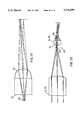
- FIG. 1illustrates a prior art optical system
- FIG. 2schematically illustrates an exemplary lenslet array system
- FIG. 3shows schematically a sectional view of a lenslet array system 100 of a first embodiment
- FIG. 4illustrates the positioning of lenslets 130 and 140 of the lenslet array system 100 relative to one another and relative to the intermediate image plane;
- FIG. 5shows a top view of the baffle plate 150 and the lenslets 130 of the first lenslet array 110;
- FIG. 6illustrates a side view of the baffle plate 150 and the lenslet array 110
- FIG. 7illustrates the baffle structure 160
- FIGS. 8A-8Cillustrates three possible configurations of a shutter plate 170
- FIGS. 9A and 9Billustrate the second embodiment of the lenslet array system
- FIG. 10illustrates yet another embodiment of the lenslet array system
- FIG. 11illustrates the top view of the embodiment shown in FIG. 10
- FIG. 12illustrates yet another embodiment of the lenslet array system
- FIG. 13is a top view of lens contours and baffles for the lens array 10;
- FIG. 14is a sectioned view taken along the section lines 2--2 of the lens array of FIG. 13;
- FIG. 15Aillustrates in cross section a central lenslet 12 of the first lenslet array 10, 110;
- FIG. 16Aillustrate in cross section a lenslet of the first lenslet array 10, 110 at a 16 degree field angle
- FIG. 17Aillustrate in cross section a lenslet of the first lenslet array 10, 110 at a 24 degree field angle
- FIGS. 18 and 19are a front and rear perspective view of a lenslet 12
- FIG. 20is a sectioned view of the lenslet 12 of FIG. 19;
- FIGS. 21A and 21Billustrates an aperture array positioned over a lenslet array with the spherical surface of each lenslet defined with topographical lines with the lenslets physical centers diverging with respect to centers of the image sections 135 (in FIG. 21A) and converging with respect to the centers of the image sections 135 (in FIG. 21B);
- FIG. 22illustrates, in a cross section view, a first lenslet array 110 having an array of field stops and an array of aperture stops positioned in front of this lenslet array;
- FIG. 23illustrates, in a cross section view, a first lenslet array 110 having an array of field stops positioned in front of this lenslet array and an array of aperture stops positioned between the lenslet array 110 and the intermediate image plane 136;
- FIG. 24Aillustrates a cross section of the portion of a lenslet 10, 130 associated with a 0 degree field angle
- FIG. 25Aillustrates a cross section of the portion of a lenslet 10, 130 associated with a 14 degree field angle
- FIG. 26Aillustrates a cross section of the portion of a lenslet 10, 130 associated with a 20 degree field angle
- FIG. 27illustrates a cross section of a centrally located lenslet 10, 140 used in a reimaging lenslet array
- FIG. 28illustrates a small part of a lenslet array system incorporating an integral field lens reimager array.
- the lenslet array system of the present inventionis an imaging system--it creates an image I of an extended object O. It is capable of accepting a wide field of view (at least ⁇ 30 and preferably ⁇ 35 or more degrees). However, it may be beneficial for use in systems accepting a ⁇ 10° (or larger) field of view.
- the lenslet array systemcomprises a plurality (at least two) of lenslet arrays 10 which are shown in FIG. 2. It is preferred that the total length of the lenslet array system is less than 17 mm and preferably less than 12 mm, and more preferably less than 8 mm and most preferably less than 5 mm. This allows for the fabrication of extremely compact photographic and digital cameras, as well as video camcoders.
- the fist lenslet array arrays 10functions as an imaging lens and the other lenslet array functions as a relay lens (also called a reimaging lens). In addition, it may also function as an field lens.
- Each lenslet arraycomprises a plurality (over 4) of small lens elements 12. These small lens elements are called lenslets.
- a given lenslet arraymay contain tenths, hundreds, thousands or millions of lenslets 12.
- the optical powers of the lenslets 12 of lenslet arrays 10are being such that the lenslet array system has a focal length between about 0.5 and 15 millimeters. Lenslets 12 with typically have clear aperture diameters of about 1-2 millimeters.
- the lenslets 12are arranged on a common substrate 13. It is preferred that this substrate be about 0.5 to 2.5 mm thick. It may be thicker, but additional thickness is undesirable because it makes the overall lenslet array system less compact. If this substrate is made too thin it may become fragile. Thus, it is most preferred that the substrate thickness be 1-2 mm.
- the specific parameters for the exemplary lensletsare provided in the "Lens component description" of the specification.
- the lenslet array system 100comprises a plurality of lenslet arrays 10 which include a first lenslet array 110 and a second lenslet array 120 which are shown in FIG. 3.
- Lenslets 12 of the first lenslet array 110are called lenslets 130.
- Each lenslet 130has positive optical power. It has a focal length f 1 of 3.0 mm and an F-number F/2.
- Each lenslet 130functions as a separate imaging lens.
- Each lenslet 130is shaped to accept a unique segment of the field of view and to create an inverted image section corresponding to this segment of the field of view. That is, each lenslet 130 creates a small, discrete, inverted section 135 of the overall image.
- the multiple image sectionsare not continuous and are not oriented properly with one another to permit either a direct viewing or film photography (see FIG. 3).
- the second lenslet array 120is needed to reimage the multiple image sections 135 (located at the intermediate image plane 136) created by the first lenslet array 110 to form a single, continuous, correctly oriented image I out of these multiple images sections 135. More specifically, lenslets 12 of the second lenslet array 120 are called lenslets 140. These lenslets 140 have positive optical power, a focal length f 2 of 0.5 mm and the F-number F/2. Each lenslet 140 corresponds to one of the plurality of lenslets 130 on the first lenslet array 110. Each lenslet 140 functions as a relay lens. That is, each lenslet 140 of the second lenslet array 120 reimages and reinverts an image section 135 created by its corresponding lenslet 130 of the first lenslet array 110.
- the image Imay be formed on any photosensitive surface including photographic film, paper or a CCD array. It may be preferred in some digital camera application that the image I created on the photosensitive pixels of the sensing array not be continuous, because these pixels are not located substantially adjacent to one another. In this case the lenslets 140 reimage the plurality of "scrambled" image sections 135 into a plurality of the unscrambled final image sections that form an overall, correctly oriented, discontinuous image I of the object O.
- the focal lengths f 1 of lenslets 130are relatively small, preferably smaller than about 15 millimeters and more preferably smaller than 12 millimeters and even more preferably smaller than about 10 millimeters. Most preferably it will be in the 2 to 7 mm range. As stated above, in this embodiment it is 3 mm. It may be as small as 1 mm or 0.5 mm.
- the smaller is the focal length f 1the more compact is the total length of the lenslet array system. However, the smaller is the focal length f 1 (given specified field of view for each of the lenslet 120), the smaller is the size of an intermediate image section 135.
- f 1is in the range of 1 mm to 0.5 mm (or smaller) the size of the image sections 135 may become to small for their proper reimaging on film.
- the film grain sizewill be one of the major factors determining the smallest possible size for the image sections 135.
- the size of the focal length f 1may be limited by the size of the photosensitive pixels. Therefore, it is preferred that f 1 be larger than 0.5 mm and preferably larger than 1 mm.
- FIG. 3illustrates that the first lenslet array 110 forms image sections 135 (on an intermediate image plane 136) of an object O which is located at an object distance d 1 from the front vertex of the central lenslet 130.
- the object distance d 1be equal to more than 20 times the focal length f 1 of the lenslet 130 (i.e., d 1 is greater than 20 times f 1 , where f 1 is less than about 15 mm).
- any object which is located at a typical viewing distance for the camera type applicationsi.e. 300 mm or more in front of the camera
- the intermediate image plane 136serves as an object plane for the lenslet array 120 and should be located a distance d 2 behind the focal plane F of the first array, the distance d being smaller than 5% of f 1 . Therefore, this lenslet array system embodiment is insensitive to the changes in the object position. This is schematically illustrated in FIG. 4, where the distance d 2 is shown greatly exaggerated.
- the ratio f 1 to f 2be between 1 and 10, where f 1 is the focal length of the front lenslet array 110 and f 2 is the focal length of the rear, lenslet array 120. It is even more preferred that this ratio be between 1 and 7 and most preferred to be between 1 and 5. The shorter the f 2 the more compact is the overall lenslet array system. If the ratio of the two focal lengths f 1 /f 2 becomes smaller than 1, the back focus distance tend to become too large, and the lenslet array system tends to become less compact.
- f 1is 3.0 mm and f 2 is 0.5 mm.
- the value of the ratio f 1 /f 2is 6.0. If a shutter is located between the two lenslets arrays, the distance between the intermediate image plane and the second lenslet array 120 should be greater or equal to about 1.2 ⁇ f 2 in order to provide enough space between the shutter and the second lenslet array 120.
- the individual lenslets 130 of the first lenslet arraysee relatively large fields of view, they form image sections 135 which are relatively large in size. Applicant discovered that some of the field light rays emerging from the edges of the intermediate image segments 135 may miss clear apertures of lenslets 140. This configuration and positioning is discussed in more detail in description of the third and fourth embodiments. Alternatively, a separate field lens array may be used. This is discussed in the description of the second embodiment.
- An opaque baffle plate 150 having multiple openings 155is positioned in front of the lenslet array 110. (FIG. 5 and 6). It may serve as an aperture stop array.
- the openings 155 of the plate 150are aligned with the individual lenslets 130 to allow the proper light beams to go through the lenslet array system.
- the size and the shape of the lenslets 130match the size and the shapes of the openings 155.
- the opaque portion of the plate 150prevents the light rays from passing between the lens elements, from propagating further into the lenslet array system as unwanted (also referred to as stray) light, and from reducing image quality.
- the function of the baffle plate 150may also be incorporated into the structure of the lenslet array 110 by making the substrate of the lenslet array 110 opaque to light in all areas not occupied by the lenslets 130.
- the field of view of the first lenslet array 110is limited by an opaque baffle structure 160.
- the baffle structure 160includes a field limiting opaque plate 162 with a plurality of apertures 165, and a plurality of baffle walls 167. These baffle walls 167 absorb stray light rays (A) exiting lenslet 130 and thus prevent it from ether propagating towards another (inappropriate) image segment 135 or from reflecting off the walls and propagating towards the image segment associated with the specific lens element 130.
- the baffle walls 167may also serve as spacers between the lenslet array 110 and the intermediate image plane.
- the opaque plate 162 with a plurality of apertures 165functions as a field stop.
- the opaque plate 162is located at or near the intermediate image plane 136.
- Each aperture 165frames a small image section 135 created by one of the lenslets 130 and in combination with the opaque section of the plate 162 surrounding this aperture serves as a field stop for this lenslet.
- the opaque section of the plate 162also blocks unwanted field rays B and prevents these rays from propagating towards the relay lenslet array 120.
- a shutter 170is located in a vicinity of the plate 162. It is composed of a series of holes 175 in an opaque shutter plate 172. The examples of shutter 170 are schematically illustrated in FIG. 8A-8C.
- the shutter 170may be located in front or behind the intermediate image plane.
- the holes 175 of the shutter 170are aligned with the opaque areas of the field limiting plate 162, but can be displaced, for example by a spring operated mechanism M, to align with the holes 165 (FIG. 7) in order to expose the photosensitive medium for the desired amount of time.
- the intermediate image sections located at or near the focal plane of the imaging lenslets 130must be equal or smaller than 1/2 the spacings d' between (the centers of) lenslets 130.
- a different shutter arrangementmay also be utilized.
- conventional shutterssuch as a focal plane shutter, or an iris shutter located in font of the lenslet array system may be used to prevent the photosensitive area from being exposed. If a conventional shutter is used, the spacing between the image sections 135 may be smaller or larger than 1/2 spacing between the centers of the lenslets.
- Lenslet array system 200 of the second embodiment of the present inventionis schematically illustrated in FIGS. 9A and 9B.
- Lenslet array system 200comprises three lenslets arrays 110, 115, and 120.
- Lenslet arrays 110 and 120 of the second embodimentserve the same function as lenslet arrays of 110 an 120 of the first embodiment.
- the lenslet array 110is the imaging lenslet array and the lenslet array 120 is the relay array.
- Lenslet array 120comprises a plurality of lenslets 140.
- the Lenslet array 115serves the function of the field lens. It is located at or near the intermediate image plane and bends the field rays towards the optical axis of the individual lenslet, making the lens bundles incident on each of the lenslets 140 smaller.
- the field lenslet array 115is especially useful in a lenslet array system with a large field of view because it sends more light rays towards the lenslet array 120 and thus allows for the smaller size lenslets 140 in the lenslet array 120.
- the field plate 162 and the shutter 170may be located either in front or behind the field lens array 115.
- FIG. 9Ashows the field lens array 115 located in front of the field plate and the shutter
- FIG. 9Bshows the field lens array 115 located in behind of the field plate and the shutter.
- the holes 175 of the shutter 170are aligned with the opaque areas of the field limiting plate 162, but can be displaced, for example by a spring operated mechanism M, to align with the holes 165 in order to expose the photosensitive medium for the desired amount of time.
- FIG. 9Athe shutter is in the closed position
- FIG. 9Bthe shutter is shown in the open position.
- the intermediate image plane 136serves as an object plane for the lenslet array 120 and should be located a distance d 2 behind the focal plane F of the first array, the distance d 2 being ⁇ 5% of f 1 . Therefore, this lenslet array system embodiment is insensitive to the changes in the object position.
- Lenslet array system 300 of the third embodiment of the present inventionis schematically illustrated in FIG. 10.
- Lenslet array system 300comprises two lenslets arrays 110, and 120.
- Lenslet arrays 110 and 120 of the lenslet array system 300serve the same function as lenslet arrays of 110 an 120 of the first embodiment.
- the lenslet array 110is the imaging lenslet array. It is made of a plurality of lenslets 130.
- all of the lenslets 130, with an exception of a center lensletare decentered lenslets. That is, their individual optical axis 18 and their unit cell axis of symmetry 14 do not overlap. This is illustrated in FIG. 11.
- the unit cell axis of symmetryis defined as an axis of symmetry of the space occupied by an individual lenslet.
- lenslet 110The parameters for an exemplary lenslet 110 are described in detail in the "Lens component description" of the specification.
- This arrangement of lenslets on the lenslet array 110allows each of the individual image segments 135 to be centered on the unit cell axis 14 of corresponding lenslet 130.
- the optical axis 18' of the second lenslet array 120may then be collinear with the unit cell axis 14 of the first lenslet array 110. This allows for a very compact lenslet array system.
- the lenslet array 120is the relay (or reimager) lenslet array.
- the lenslet array 120reimages the multiple, inverted image segments 135 located at the intermediate image plane into a continuous, correctly oriented image located at the final image plane.
- the lenslet array 120serves the function of the field lens. That is, lenslet array 120 of this embodiment is a field lens array. More specifically, the front (object facing) surface S 3 of lenslet 140 is located at or in the vicinity of the intermediate image plane 136 and bends the field rays C towards the optical axis 18' of this lenslet.
- the surface S 3is spaced slightly away from the intermediate image plane so that the dust particles or scratches present on the surface S 3 would not be reimaged onto the final image plane.
- the rear surface S 4i.e., the surface facing the final image plane
- the final size of the imageis about the same as the size of the lenslet array 120.
- the baffling system employed in lenslet array system 300is similar to the one employed by the lenslet array system 100 and 200 and is also shown schematically in FIG. 10. It includes an opaque baffle layer 150 with multiple transmissive sections or apertures 155, and a baffling structure 160 which is similar to the baffling structure 160 of the lenslet array system 100.
- a shuttersimilar to the shutter 170, is located behind the baffling plate 162.
- the size of the image sections 135 located at the intermediate image plane 136must be smaller than 1/2 spacing d' between lenslet unit cell centers. However, if a different shutter arrangement is utilized, the size of the image sections 135 may be larger.
- Lenslet array system 400 of the third embodiment of the present inventionis schematically illustrated in FIG. 12.
- Lenslet array system 400comprises two lenslets arrays 110, and 120.
- Lenslet arrays 110 and 120serve the same function as lenslet arrays of 110 an 120 of the third embodiment.
- the lenslet array 110is the imaging lenslet array. It is made of a plurality of lenslets 130. All of the lenslets 130, with an exception of a center lenslet are "tilted" lenslets. That is, the central ray in their field of view is not perpendicular to the intermediate image plane 136. This arrangement is described in detail in the "Lens component description" of the specification.
- the lenslet array 120is the relay (or reimager) lenslet array and comprises a plurality of lenslets 140.
- the lenslet array 120is also designed to serve as a field lens array.
- the front surfaces of lenslets 140are convex.
- the front (object facing) surface of the lenslet array 120is located at or in the vicinity of the intermediate image plane and bends the field rays towards the optical axis 18' of the lenslet 140 of the second lenslet array 120.
- the rear lenslet surface S 4i.e., the surface facing the final image plane
- the lenslet array 120reimages the multiple, inverted image segments 135 located at the intermediate image plane into a correctly oriented image located at the final image plane. This image is continuous if the lenslet array system images on film. It may be continuous or discontinuous if a CCD or a similar array is used as a photosensitive surface.
- the lenslet array system 400is not as compact as lenslet array system 300. This is because in order to achieve the same final image size, as achieved by the lenslet array system 300, the lenslet array 110 of the lenslet array system 400 needs to be larger than the lenslet array 120.
- a lenslet array 10is formed with an array of achromatized refractive/diffractive lenslets 12 or refractive lenslets. Such an array may be used as first array 110 in the first, the second or the third lenslet array system embodiment, respectively. These embodiments are described in the "lenslet array system description" section of this application. To be observed in this figure is that the center of the optical axis 18 of each lenslet 12 is displaced by a distance d relative to the fixed unit cell to unit cell distance X as a function of its radial distance from the optical axis of the central lenslet.
- the lines 15 appearing around the optical axis 18 of each lenslet 12are topographical lines indicating changes in height of the lenslet's surface.
- An opaque mask 16fills the areas between the lenslets 12 to prevent stray light from propagating farther into the optical system.
- the array depicted in FIG. 13represents only a small portion of an array that will be used in an actual camera. In an actual implementation many more lenslets are used to form the array. Other configurations of the lenslets 12 may be used such as forming the outer periphery of each lenslet as a square, hexagon, or circle, without detracting from the invention.
- the optical axis 18 of the lenslets 12 in the lenslet arrayare located at a distance which becomes progressively larger than the center-to-center distance of the unit sells of the lenslet array.
- the displacement d of the lenslets optical axis 18increases radially from the center of the array. Decentering a lenslet tends to bend rays from off-axis field angles to be incident perpendicular to the intermediate image plane.
- the optical axis 18 of the lensletBy moving the optical axis 18 of the lenslet further out radially with increasing distance from the center of the array, the angular location of object at the center of the field of view for a given lenslet originates from increasingly off-axis segments of the total field of view (see FIG. 14).
- the required decenter for a lenslet 12 of focal length FL i necessary to deflect the ray from the desired field angle into the center of the array element's field stopcan be determined from the paraxial ray tracing equations.
- the paraxial equationsare
- nrefractive index of the medium
- the inventionutilizes an array of lenslets where the local displacement of the lenslets optical axis varies as a function of radial position relative to the center of the lenslet array system's optical axis, so that, to first order
- the decenter d necessary for a given elementis approximately a linear function of the element's radial distance from the system's optical axis.
- the lenslet array 10is positioned over an intermediate image plane and creates a plurality of image segments 135.
- a shuttermay be located next to the intermediate image plane 136.
- the lens array 10is maintained a distance apart from the shutter by spacers 22 that may also serve the function of being baffles.
- the opaque baffles 16 on the lenslet array 10may be combined with a field stop (aperture plate 40) to limit the field of view of any particular photosensor so that it does not overlap the field of view of it neighbors by a large amount.
- the aperture plate 40is preferably positioned approximately 0.5 mm to 2 mm from the surface of the lenslet array 10.
- the aperture plate 40may be a layer of clear glass having a dyed photoresist mask pattern formed on one of its surfaces.
- the center of the apertures in the aperture plate 40are aligned to the center of the field of view (CFDV) of a corresponding lenslet.
- the spacing of the centers of apertures in the plate 40increases as a function of each lenslet's radial position radially from the center of the array causing the aperture plate to be slightly larger than the associated lens array.
- the combination of the opaque areas 16 with the aperture plate 40 and/or the field limiting plate 162, and a given lenslet focal lengthdetermines the field of view for a particular lenslet on the lenslet array.
- the lenslet array 10can be formed by etching a photosensitive pattern into quartz, or formed as an epoxy replica on a quartz substrate or as a photoresist substrate relief part on a glass substrate, or be injection molded as a plastic part.
- the lenslets 12By forming the lenslets 12 with decentrations d of the optical axis 18 which increase radially across the lenslet array, the angle which the ray beam incident on any of the lenslet 12 will increase as a function of radial position of this lenslet on the array. Therefore, by appropriately adjusting the decenters of each lenslet each image section corresponds to a unique or different segment of the scene.
- Lenslet array 10may an array of aspheric lenslets to improve the lenslet array system performance.
- aspheric lensletsdo not correct for the variation in focal length as a function of wavelength if these lenslets are formed from a single refractive material. That is, the spot sizes at the image plane will vary as a function of color.
- an improved lenslet array system including an array of diffractive/refractive hybrid lensletsmay be used instead of an array of purely refractive lenslets.
- the imaging properties of diffractive opticsare strongly wavelength dependent. When modeling a diffractive optic this phenomena can be represented as a direct dependence of equivalent refractive index n( ⁇ ) on wavelength( ⁇ ):
- ⁇ diffFor other wavelength bands of interest an appropriate ⁇ diff , and element power distribution can be calculated.
- a single element lensDue to the variation of refractive index with wavelength, a single element lens has a variation of focal length with wavelength. Two materials with different dispersions can be used to form a doublet lens which has the same focal length at two wavelengths and reduced variation over the whole spectrum. The relative distribution of focal powers required to achieve this is given by ##EQU3##
- the negative ⁇ diff of the diffractive surfaceallows for achromatization of single element hybrid refractive/diffractive lenses utilizing a positive focal length diffractive and refractive component. It also decreases the focal length and F/# required of the doublet component lenses because a refractive doublet consists of a positive crown (low dispersion) lens with a shorter focal length and smaller F/# than is required for a singlet and a negative flint element which increases the doublet focal length to the correct value and compensates for the dispersion of the positive lens. This effect also decreases the size and weight of the positive element of a hybrid refractive/diffractive element.
- diffractive/refractive hybrid achromatizationenables the use of diffractive surfaces with longer focal lengths and higher F-numbers.
- the diffractive lenslets 12are shown in FIGS. 15A, 16A, and 17A, for the on-axis, 16 degrees, and full field of view. To be noted in a comparison of these figures is that the optical axis 18 is moving radially outwards as a function of field angle. It is noted that the opaque baffle 16 acts as the aperture stop for the system and limits the field of view of a given lenslet 12.
- the following tablelists the optical design parameters for three array elements at 0, 16, and 24 degrees.
- the array elements at the intermediate field anglescan be interpolated from these values.
- the first lenslet 12, 130is one element of a first lenslet array 110 that is formed with a number of lenslets. Such an array may be used as a first lenslet array in the first, second or fourth lenslet array system embodiments, respectively.
- Each lenslet (12, 130)is formed with a diffractive pattern S' formed on a refractive, spherical surface S 1 . Opposite the surface S 1 is a second surface S 2 Surface S 2 is an aspheric surface. The faceted surface of the diffractive pattern S' is seen more clearly in the cross-section of FIG. 20.
- the second surface S 2is convex and transforms to a concave surface at the radius R 2 (where R 2 is greater than R 1 ).
- the second surface S 2is defined by a polynomial asphere which exhibits an inflection at the radius R 3 (where R 3 is greater than R 2 ).
- Both the first and the second surfacesare substantially perpendicular to the optical axis 18 of the lenslet 12.
- the lenslet 12may be formed as an epoxy replica via use of a quartz or a photoresist mask on a glass substrate, or be injection molded as a plastic part.
- incident light rays 30pass through an aperture stop array 40 and are focused onto a focal plane (F,50) by the lenslet 12, 130.
- the diffractive/refractive surface comprised of S 1 and S'corrects the chromatic aberrations and provides the majority of the focusing power while the aspheric surface S 2 provides for correction of field dependent aberrations such as petzval curvature, astigmatism, and coma.
- the lenshas an F# of 2.0 and a FL of 0.5 mm.
- FIGS. 21A and 21BThe individual lenslets 12 of FIGS. 20 and 21 are segmented and formed into a lenslet array 10.
- the center of the optical axis 18 of each lenslet 12is displaced outward as a function of its radial distance from the optical axis of the central lenslet while in FIG. 21B, the optical axes 18 are displaced inward.
- the lines 15 appearing around the optical axis 18 of each lenslet 12are topographical lines generally indicating changes in height of the lenslet's surface.
- An array of opaque baffles 16also serving as an aperture stop fills the areas between the lenslets 12 to prevent stray light from reaching further into the lenslet array system.
- FIGS. 21A and 21Brepresent only a small portion of an array that would be used in an actual camera.
- the optical axis of each lenslet, and in turn the lenslet itselfis not aligned directly over its corresponding image section. Instead the lenslets are displaced so as to form image sections 135 at regularly spaced intervals on the intermediate image plane 136.
- Other configurations of the lensletsmay be used such as forming the outer periphery of each lenslet as a square, hexagon, or circle, without detracting from the invention.
- the reason that the invention uses only portions of the lensletsis that only a fraction of the lenslet is used for a particular angular field of view for an image section.
- FIG. 22 and 23show cross-sections taken along the section line 4--4 in FIGS. 21A and 21B, illustrating the lenslet array 10, 110 positioned over the intermediate image plan and forming a number of image sections 135 corresponding in number to at least the number of lenslets forming the array 10, 110.
- the lenslet array 10, 110is maintained a distance apart from the intermediate image plane by spacers 167 that also serve the function of being baffle walls.
- the aperture stop array 40in combination with the baffle walls 167 and the field stop array 42 limit the field of view of any image section so that it does not overlap the field of view of it neighbors by a large amount.
- the field stop array 42is positioned approximately 0.5 mm to 2 mm from the surface of the lenslet array 10.
- the center of the apertures in the aperture stop array and field stop array, 40 and 42, respectivelyare aligned to the center of the field of view of a corresponding lenslet.
- the spacing of the centersincreases as a function of each lenslet's field angle from the center of the array causing the aperture stop array to be slightly larger than the associated lenslet array.
- the combination of the aperture stop array 40 with the field stop array 42 and a given lenslet focal lengthdetermines the field of each of the lenslets and the position of image sections on the intermediate image plane.
- an improved lenslet arrays including a diffractive/refractive hybrid lensletsis used to correct the chromatic aberration present due to use of a single refractive material.
- the diffractive lenslets 12are shown in FIGS. 24A, 25A, and 26A, for the on-axis, 14 degrees, and full field of view.
- the optical axis 18is moving radially outwards as a function of field angle while the unit cell 14 is incident normal to the plane of the intermediate image plane 136.
- the opaque mask 16acts as the aperture stop for the system as well as limiting the field of view of a given lenslet.
- the aspheric surface profileis defined by equation (1) ##EQU6##
- the diffractive phase profilerotationally symmetric and is defined as ##EQU7##
- a relay lenslet array 10is formed with an array of refractive lenslets 12. Such an array may be used as second (reimaging) lenslet array 120.
- the lensletsare formed of glass. They have an effective focal length if 0.5 mm.
- the following tablelists the optical design parameters for a centrally located lenslet comprising array 120. This lenslet is illustrated in FIG. 27.
- a lenslet array systemsuch as the lenslet array system 300 shown in FIGS. 10 and 12 includes a first, imaging lenslet array 110 having a plurality of lenslets 130 and a second lenslet array 120 having a plurality of lenslets 140.
- the second lenslet array 120 of the third lenslet array system embodiment 300is an integral field lens/reimager lenslet array.
- This array 120may be formed with an array of achromatized refractive/diffractive lenslets 12, 140 or refractive lenslets.
- the lenslet array system 300is described in the "lenslet array system description" section of this application. As can be seen from the drawing (FIG.
- the front (object side) surface S 3 of the lenslets 12 of the integral field lens/reimager lenslet array lenslet array 120is convex and is located close to the intermediate image plane 136.
- the surface S 3performs the function of the field lens. It is preferred that the front surface S 3 of these lenslets be slightly spaced (about 1 mm or less) from the intermediate image plane so that the dust particles or surface scratches located at the surface S 3 would not get reimaged onto the final image plane 136. In this example the front surface S 3 of the reimaging lenslets 12 of the second lenslet array is located 0.19 mm away from the intermediate image plane.
- Surface S 4 of the lenslet 140performs (primarily) the relaying function--i.e.
Landscapes
- Physics & Mathematics (AREA)
- General Physics & Mathematics (AREA)
- Optics & Photonics (AREA)
- Lenses (AREA)
Abstract
Description
y'=y.sub.o +nu(t/n)
n'u'=n.sub.o u.sub.o -yφ
d=y=(n.sub.o u.sub.o -n'u')/FL.sub.i)
d(r)=(n.sub.o u.sub.o (r)-n'u'(r))/FL.sub.i
n(λ)= λ.sub.c /λ!(n.sub.c -1)-1
f(λ)= n(λ)-1!Δc
f(λ)=(λ.sub.c /λ)f.sub.c
.sup.Φ ref/.sup.Φ total=94.25%
.sup.Φ diff/.sup.Φ total=5.75%
.sup.f ref=3.186 mm F/#=2.12
.sup.f diff=52.176 mm F/#=34.8
TABLE 1 ______________________________________ Surface No. Radius Thickness Glass ______________________________________ Object Infinity Air 1 Aperture Stop 2.0 BK7 2 -1.639 3.0 Air Aspheric Coeff. k = 0.973 Diffractive DF3 = -8.2 × 10.sup.-3 AD = 1.04 × 10.sup.-1 Coeff. DF5 = -8.4 × 10.sup.-3 AE = -3.35 × 10.sup.-2 DF10 = -8.3 × 10.sup.-5 AF = 1.17 × 10.sup.-1 DF14 = 1.4 × 10.sup.-3 AG = -7.75 × 10.sup.-2 Element DF21 = 4.5 × 10.sup.-4 Decenter DF27 = -2.3 × 10.sup.-3 DC = 0.0 Image Air ______________________________________
TABLE 2 ______________________________________ Surface No. Radius Thickness Glass ______________________________________ Object Infinity Air 1 Aperture Stop 2.0 BK7 2 -1.602 3.0Air 2 Aspheric Coeff. k = -0.670 Diffractive DF3 = -4.8 × 10.sup.-4 AD = -7.0 × 10.sup.-3 Coeff. DF5 = -4.7 × 10.sup.-3 AE = 2.1 × 10.sup.-2 DF10 = 1.4 × 10.sup.-2 AF = -5.9 × 10.sup.-3 DFl4 = -3.6 × 10.sup.-3 AG = 6.5 × 10.sup.-4 DF21 = -5.2 × 10.sup.-3 Element DF27 = 6.2 × 10.sup.-4 Decenter DC = -0.513 Image Air ______________________________________
TABLE 3 ______________________________________ Surface No. Radius Thickness Glass ______________________________________ Object Infinity Air 1 Aperture Stop 0.5 BK7 2 -1.509 0.391 Air Aspheric Coeff. k = -0.570 Diffractive DF3 = 7.8 × 10.sup.-3 AD = 0.0 Coeff. DF5 = 5.2 × 10.sup.-3 AE = -4.6 × 10.sup.-3 DF10 = 1.0 × 10.sup.-2 AF = 9.5 × 10.sup.-3 DF14 = -6.3 × 10.sup.-2 AG = -1.2 × 10.sup.-3 DF21 = -2.9 × 10.sup.-3 AH = 1.4 × 10.sup.-4 Element DF27 = 7.3 × 10.sup.-4 Decenter DC = -0.872 Image Air ______________________________________
TABLE 4 ______________________________________ Surface No. Radius Thickness Glass ______________________________________ Object Infinity Air 1 Aperture Infinity 0.9083Air Stop 2 2.805 2.9999 BK7 Diffractive DF1 = 1.058410.sup.-2 Coefficients DF2 = 9.572 × 10.sup.-4 3 -2.417 1.704 Air Aspheric AD = 0.3245 × 10.sup.-1 Coefficients AE = 0.4534 × 10.sup.-2 Image Air ______________________________________
λ.sub.0 =546.1 nm
TABLE 5 ______________________________________ Surface No. Radius Thickness Glass ______________________________________ Object 0.19 Air 1 infinity 0.8BK7 2 Aperture Stop -0.25936* 1.548 AIR Aspheric Coeff. k = 0.0 AD = -0.332E + 01 AE = 0.833E + 03 AF = -0.216E + 05 AG = 0.67373E + 05 Image Air ______________________________________ *Aspheric surface. The aspheric surface profile is defined by equation 1 listed above.
TABLE 6 ______________________________________ Surface No. Radius Thickness Glass ______________________________________ Object Air 1, Aperture infinity 2.0 BK7 Stop 2.* -1.657 3.0 Air Aspheric k = 1.0175 Diffractive DF3 = -1.002E - 02 Coeff.: AD = 1.0159E - 01 Coeff.: DF5 = -1.029E - 02 AE = -8.4538E - 02 DF10 = -1.813E - 03 AF = 2.5147E - 01 DF14 = 1.6915E - 04 AG = -1.9531E - 01 DF21 = 3.389E - 03 DF27 = 2.345E - 04 3 infinity 0.19air 4 0.847 0.5 BK7 5 infinity 0.3 BK7 6 -0.25936 1.547895 air Aspheric k = 0.0 Coeff. AD = 0.126E + 02 AE = 0.1688E + 01 AF = 0.7923E + 03 AG = 0.16542E + 05 Image Air ______________________________________ *Surface 2 is an aspheric surface with a diffractive pattern which is formed on this aspheric surface.Surface 2 is a rotationally symmetric surface. Its profile is defined by the equation 1
Claims (8)
Priority Applications (1)
| Application Number | Priority Date | Filing Date | Title |
|---|---|---|---|
| US08/771,592US5731899A (en) | 1996-12-20 | 1996-12-20 | Lenslet array system incorporating an integral field lens/reimager lenslet array |
Applications Claiming Priority (1)
| Application Number | Priority Date | Filing Date | Title |
|---|---|---|---|
| US08/771,592US5731899A (en) | 1996-12-20 | 1996-12-20 | Lenslet array system incorporating an integral field lens/reimager lenslet array |
Publications (1)
| Publication Number | Publication Date |
|---|---|
| US5731899Atrue US5731899A (en) | 1998-03-24 |
Family
ID=25092319
Family Applications (1)
| Application Number | Title | Priority Date | Filing Date |
|---|---|---|---|
| US08/771,592Expired - LifetimeUS5731899A (en) | 1996-12-20 | 1996-12-20 | Lenslet array system incorporating an integral field lens/reimager lenslet array |
Country Status (1)
| Country | Link |
|---|---|
| US (1) | US5731899A (en) |
Cited By (53)
| Publication number | Priority date | Publication date | Assignee | Title |
|---|---|---|---|---|
| US5857042A (en)* | 1997-04-29 | 1999-01-05 | Mcgill University | Optical interconnection arrangements |
| US6278500B1 (en)* | 1998-10-06 | 2001-08-21 | Seiko Epson Corporation | Liquid crystal device and projector display device having a specific relationship for the F-numbers of the illumination optical system |
| US6324149B1 (en)* | 1997-05-27 | 2001-11-27 | Ricoh Company, Ltd. | Optical-pick-up device achieving accurate positioning of objective lens and solid-immersion lens and method of forming same |
| US6483535B1 (en) | 1999-12-23 | 2002-11-19 | Welch Allyn, Inc. | Wide angle lens system for electronic imagers having long exit pupil distances |
| US6657749B1 (en)* | 1998-10-01 | 2003-12-02 | Honeywell International Inc. | Scanner using lens array producing inverted images |
| US20040040764A1 (en)* | 2002-08-30 | 2004-03-04 | Polak Anthony J. | Automotive drive assistance system and method |
| US20040119104A1 (en)* | 2002-12-20 | 2004-06-24 | Eastman Kodak Company | Imaging system having extended useful latitude |
| US20040179834A1 (en)* | 2003-03-14 | 2004-09-16 | Eastman Kodak Company | Camera using beam splitter with micro-lens image amplification |
| US20040218288A1 (en)* | 2003-05-02 | 2004-11-04 | International Business Machines Corporation | Optical communication assembly |
| US20040217464A1 (en)* | 2003-05-02 | 2004-11-04 | International Business Machines Corporation | Optical assemblies for transmitting and manipulating optical beams |
| US20050046734A1 (en)* | 2003-08-26 | 2005-03-03 | Eastman Kodak Company | Photographic film cartridge or cassette systems with microlens |
| US20050206772A1 (en)* | 2003-10-10 | 2005-09-22 | Ruling Optics, Llc | Optical imaging device |
| US20060044451A1 (en)* | 2004-08-30 | 2006-03-02 | Eastman Kodak Company | Wide angle lenslet camera |
| US20060170810A1 (en)* | 2005-02-03 | 2006-08-03 | Samsung Electronics Co., Ltd. | Methods of manufacturing microlenses, microlens arrays and image sensors |
| US20060192083A1 (en)* | 2005-02-25 | 2006-08-31 | Taiwan Semiconductor Manufacturing Company, Ltd. | Methods to Improve Photonic Performances of Photo-Sensitive Integrated Circuits |
| US7164518B2 (en) | 2003-10-10 | 2007-01-16 | Yuping Yang | Fast scanner with rotatable mirror and image processing system |
| US20070014022A1 (en)* | 2005-07-15 | 2007-01-18 | Pixon Technologies Crop | Lens array |
| US7307790B1 (en)* | 2006-11-10 | 2007-12-11 | Genie Lens Technologies, Llc | Ultrathin lens arrays for viewing interlaced images |
| US20080112056A1 (en)* | 2006-11-10 | 2008-05-15 | Genie Lens Technologies, Llc | Ultrathin lens arrays for viewing interlaced images with dual lens structures |
| US20080150174A1 (en)* | 2006-11-10 | 2008-06-26 | Genie Lens Technologies, Llc | Manufacture of display devices with ultrathin lins arrays for viewing interlaced images |
| US20080173791A1 (en)* | 2007-01-19 | 2008-07-24 | Palum Russell J | Image sensor with three sets of microlenses |
| US7480100B1 (en) | 2007-10-15 | 2009-01-20 | Genie Lens Technologies, Llc | Lenticular devices using sets of lenses to display paired sets of interlaces of images |
| US20090147368A1 (en)* | 2007-12-10 | 2009-06-11 | Samsung Electro-Mechanics Co., Ltd. | Method for manufacturing wafer scale lens assembly and wafer scale lens assembly manufactured by the same |
| US20100080002A1 (en)* | 2008-09-30 | 2010-04-01 | Tyco Electronics Corporation | Color homogenizing optical assembly |
| WO2012040414A3 (en)* | 2010-09-23 | 2012-06-21 | Light Prescriptions Innovators, Llc | Shell integrator |
| CN104049334A (en)* | 2014-07-03 | 2014-09-17 | 南昌欧菲光电技术有限公司 | Camera shooting module |
| US20150138547A1 (en)* | 2012-05-07 | 2015-05-21 | Elmos Semiconductor Ag | Apparatus for selectively transmitting the spectrum of electromagnetic radiation within a predefined wavelength range |
| US9191661B2 (en) | 2011-08-29 | 2015-11-17 | Microsoft Technology Licensing, Llc | Virtual image display device |
| CN105301677A (en)* | 2014-06-03 | 2016-02-03 | 佳能株式会社 | Photomask, method of manufacturing optical element array, optical element array |
| US9709242B2 (en) | 2010-09-23 | 2017-07-18 | Light Prescriptions Innovators, Llc | Shell integrator |
| WO2017155747A1 (en)* | 2016-03-08 | 2017-09-14 | Microsoft Technology Licensing, Llc | Array-based camera lens system |
| US9967546B2 (en) | 2013-10-29 | 2018-05-08 | Vefxi Corporation | Method and apparatus for converting 2D-images and videos to 3D for consumer, commercial and professional applications |
| WO2018103819A1 (en)* | 2016-12-05 | 2018-06-14 | Photonic Sensors & Algorithms, S.L. | Microlens array |
| US10012834B2 (en) | 2016-03-08 | 2018-07-03 | Microsoft Technology Licensing, Llc | Exit pupil-forming display with reconvergent sheet |
| US10158847B2 (en) | 2014-06-19 | 2018-12-18 | Vefxi Corporation | Real—time stereo 3D and autostereoscopic 3D video and image editing |
| US10191188B2 (en) | 2016-03-08 | 2019-01-29 | Microsoft Technology Licensing, Llc | Array-based imaging relay |
| US10250864B2 (en) | 2013-10-30 | 2019-04-02 | Vefxi Corporation | Method and apparatus for generating enhanced 3D-effects for real-time and offline applications |
| WO2019156807A1 (en)* | 2018-02-07 | 2019-08-15 | Lockheed Martin Corporation | Plenoptic cellular imaging system |
| US10510812B2 (en) | 2017-11-09 | 2019-12-17 | Lockheed Martin Corporation | Display-integrated infrared emitter and sensor structures |
| US10594951B2 (en) | 2018-02-07 | 2020-03-17 | Lockheed Martin Corporation | Distributed multi-aperture camera array |
| US10652529B2 (en) | 2018-02-07 | 2020-05-12 | Lockheed Martin Corporation | In-layer Signal processing |
| US10690910B2 (en) | 2018-02-07 | 2020-06-23 | Lockheed Martin Corporation | Plenoptic cellular vision correction |
| US10698201B1 (en) | 2019-04-02 | 2020-06-30 | Lockheed Martin Corporation | Plenoptic cellular axis redirection |
| US10838250B2 (en) | 2018-02-07 | 2020-11-17 | Lockheed Martin Corporation | Display assemblies with electronically emulated transparency |
| US10866413B2 (en) | 2018-12-03 | 2020-12-15 | Lockheed Martin Corporation | Eccentric incident luminance pupil tracking |
| US10930709B2 (en) | 2017-10-03 | 2021-02-23 | Lockheed Martin Corporation | Stacked transparent pixel structures for image sensors |
| US10951883B2 (en) | 2018-02-07 | 2021-03-16 | Lockheed Martin Corporation | Distributed multi-screen array for high density display |
| CN114500809A (en)* | 2022-01-29 | 2022-05-13 | 奕目(上海)科技有限公司 | Light field lens assembly, light field lens, light field imaging device and system |
| US11454745B2 (en)* | 2018-05-30 | 2022-09-27 | Depixus | Multichannel close-up imaging device |
| US11616941B2 (en) | 2018-02-07 | 2023-03-28 | Lockheed Martin Corporation | Direct camera-to-display system |
| WO2024213719A1 (en)* | 2023-04-14 | 2024-10-17 | Ams-Osram Asia Pacific Pte. Ltd. | Projected light system compensating for low accuracy manufacturing processes |
| US12181690B2 (en) | 2022-07-06 | 2024-12-31 | Lumenco, Llc | Micro-optic anticounterfeiting elements for currency and other items using virtual lens systems |
| WO2025017209A1 (en)* | 2023-07-20 | 2025-01-23 | Fraunhofer-Gesellschaft zur Förderung der angewandten Forschung e.V. | Display, method for projecting an image and method for producing a display |
Citations (11)
| Publication number | Priority date | Publication date | Assignee | Title |
|---|---|---|---|---|
| US4632522A (en)* | 1983-10-31 | 1986-12-30 | Mita Industrial Co., Ltd. | Optical system of variable magnification and a method for varying magnification of the same |
| US4988188A (en)* | 1987-08-31 | 1991-01-29 | Canon Kabushiki Kaisha | Illumination device |
| US5101279A (en)* | 1989-12-14 | 1992-03-31 | Canon Kabushiki Kaisha | Liquid crystal display apparatus having lenticular elements oriented in relation to LC pixel aperture dimensions |
| US5270859A (en)* | 1992-01-30 | 1993-12-14 | United Technologies Corporation | Optical instrument with micro-lenses |
| US5291334A (en)* | 1992-01-30 | 1994-03-01 | United Technologies Corporation | Micro-lens panoramic imager |
| US5418583A (en)* | 1992-03-31 | 1995-05-23 | Matsushita Electric Industrial Co., Ltd. | Optical illumination system and projection display apparatus using the same |
| US5465175A (en)* | 1992-11-11 | 1995-11-07 | Sharp Kabushiki Kaisha | Autostereoscopic display device |
| US5550656A (en)* | 1992-06-17 | 1996-08-27 | Xerox Corporation | Full color display with plural two-dimensional planar arrays of lenslets |
| US5636056A (en)* | 1992-07-02 | 1997-06-03 | Singoh Denzai Kabushiki Kaisha | Device for preventing signal lamps from presenting false lighting phenomenon |
| US5648874A (en)* | 1994-06-29 | 1997-07-15 | Fujitsu Limited | Optical apparatus |
| US5650876A (en)* | 1993-03-25 | 1997-07-22 | De Montfort University | Lens system with intermediate optical transmission microlens screen |
- 1996
- 1996-12-20USUS08/771,592patent/US5731899A/ennot_activeExpired - Lifetime
Patent Citations (11)
| Publication number | Priority date | Publication date | Assignee | Title |
|---|---|---|---|---|
| US4632522A (en)* | 1983-10-31 | 1986-12-30 | Mita Industrial Co., Ltd. | Optical system of variable magnification and a method for varying magnification of the same |
| US4988188A (en)* | 1987-08-31 | 1991-01-29 | Canon Kabushiki Kaisha | Illumination device |
| US5101279A (en)* | 1989-12-14 | 1992-03-31 | Canon Kabushiki Kaisha | Liquid crystal display apparatus having lenticular elements oriented in relation to LC pixel aperture dimensions |
| US5270859A (en)* | 1992-01-30 | 1993-12-14 | United Technologies Corporation | Optical instrument with micro-lenses |
| US5291334A (en)* | 1992-01-30 | 1994-03-01 | United Technologies Corporation | Micro-lens panoramic imager |
| US5418583A (en)* | 1992-03-31 | 1995-05-23 | Matsushita Electric Industrial Co., Ltd. | Optical illumination system and projection display apparatus using the same |
| US5550656A (en)* | 1992-06-17 | 1996-08-27 | Xerox Corporation | Full color display with plural two-dimensional planar arrays of lenslets |
| US5636056A (en)* | 1992-07-02 | 1997-06-03 | Singoh Denzai Kabushiki Kaisha | Device for preventing signal lamps from presenting false lighting phenomenon |
| US5465175A (en)* | 1992-11-11 | 1995-11-07 | Sharp Kabushiki Kaisha | Autostereoscopic display device |
| US5650876A (en)* | 1993-03-25 | 1997-07-22 | De Montfort University | Lens system with intermediate optical transmission microlens screen |
| US5648874A (en)* | 1994-06-29 | 1997-07-15 | Fujitsu Limited | Optical apparatus |
Cited By (87)
| Publication number | Priority date | Publication date | Assignee | Title |
|---|---|---|---|---|
| US5857042A (en)* | 1997-04-29 | 1999-01-05 | Mcgill University | Optical interconnection arrangements |
| US6324149B1 (en)* | 1997-05-27 | 2001-11-27 | Ricoh Company, Ltd. | Optical-pick-up device achieving accurate positioning of objective lens and solid-immersion lens and method of forming same |
| US6657749B1 (en)* | 1998-10-01 | 2003-12-02 | Honeywell International Inc. | Scanner using lens array producing inverted images |
| US6278500B1 (en)* | 1998-10-06 | 2001-08-21 | Seiko Epson Corporation | Liquid crystal device and projector display device having a specific relationship for the F-numbers of the illumination optical system |
| US6483535B1 (en) | 1999-12-23 | 2002-11-19 | Welch Allyn, Inc. | Wide angle lens system for electronic imagers having long exit pupil distances |
| US20040200650A1 (en)* | 2002-08-30 | 2004-10-14 | Polak Anthony J. | Automotive drive assistance system and method |
| US20040040764A1 (en)* | 2002-08-30 | 2004-03-04 | Polak Anthony J. | Automotive drive assistance system and method |
| US7014003B2 (en) | 2002-08-30 | 2006-03-21 | Motorola, Inc. | Automotive drive assistance system and method |
| US6814171B2 (en)* | 2002-08-30 | 2004-11-09 | Motorola, Inc. | Automotive drive assistance system and method |
| US20040119104A1 (en)* | 2002-12-20 | 2004-06-24 | Eastman Kodak Company | Imaging system having extended useful latitude |
| US7423679B2 (en) | 2002-12-20 | 2008-09-09 | Eastman Kodak Company | Imaging system having extended useful latitude |
| US20040179834A1 (en)* | 2003-03-14 | 2004-09-16 | Eastman Kodak Company | Camera using beam splitter with micro-lens image amplification |
| US6801719B1 (en) | 2003-03-14 | 2004-10-05 | Eastman Kodak Company | Camera using beam splitter with micro-lens image amplification |
| US20040218288A1 (en)* | 2003-05-02 | 2004-11-04 | International Business Machines Corporation | Optical communication assembly |
| US20050078376A1 (en)* | 2003-05-02 | 2005-04-14 | Dinesh Gupta | Optical assemblies for transmitting and manipulating optical beams |
| US6922294B2 (en) | 2003-05-02 | 2005-07-26 | International Business Machines Corporation | Optical communication assembly |
| US6836015B2 (en) | 2003-05-02 | 2004-12-28 | International Business Machines Corporation | Optical assemblies for transmitting and manipulating optical beams |
| US8089133B2 (en) | 2003-05-02 | 2012-01-03 | International Business Machines Corporation | Optical assemblies for transmitting and manipulating optical beams |
| US20040217464A1 (en)* | 2003-05-02 | 2004-11-04 | International Business Machines Corporation | Optical assemblies for transmitting and manipulating optical beams |
| US20050046734A1 (en)* | 2003-08-26 | 2005-03-03 | Eastman Kodak Company | Photographic film cartridge or cassette systems with microlens |
| US7310477B2 (en) | 2003-08-26 | 2007-12-18 | Eastman Kodak Company | Photographic film cartridge or cassette systems with microlens |
| US7164518B2 (en) | 2003-10-10 | 2007-01-16 | Yuping Yang | Fast scanner with rotatable mirror and image processing system |
| US20050206772A1 (en)* | 2003-10-10 | 2005-09-22 | Ruling Optics, Llc | Optical imaging device |
| US7633655B2 (en) | 2003-10-10 | 2009-12-15 | Yuping Yang | Optical imaging device |
| US20060044451A1 (en)* | 2004-08-30 | 2006-03-02 | Eastman Kodak Company | Wide angle lenslet camera |
| US20060170810A1 (en)* | 2005-02-03 | 2006-08-03 | Samsung Electronics Co., Ltd. | Methods of manufacturing microlenses, microlens arrays and image sensors |
| US7605857B2 (en)* | 2005-02-03 | 2009-10-20 | Samsung Electronics Co., Ltd. | Methods of manufacturing microlenses, microlens arrays and image sensors |
| US20060192083A1 (en)* | 2005-02-25 | 2006-08-31 | Taiwan Semiconductor Manufacturing Company, Ltd. | Methods to Improve Photonic Performances of Photo-Sensitive Integrated Circuits |
| US7189957B2 (en) | 2005-02-25 | 2007-03-13 | Taiwan Semiconductor Manufacturing Company, Ltd. | Methods to improve photonic performances of photo-sensitive integrated circuits |
| US20070014022A1 (en)* | 2005-07-15 | 2007-01-18 | Pixon Technologies Crop | Lens array |
| US7256941B2 (en)* | 2005-07-15 | 2007-08-14 | Pixon Technologies Corp. | Lens array |
| US7731813B2 (en) | 2006-11-10 | 2010-06-08 | Genie Lens Technologies, Llc | Manufacture of display devices with ultrathin lens arrays for viewing interlaced images |
| US20080150174A1 (en)* | 2006-11-10 | 2008-06-26 | Genie Lens Technologies, Llc | Manufacture of display devices with ultrathin lins arrays for viewing interlaced images |
| US7414790B2 (en) | 2006-11-10 | 2008-08-19 | Genie Lens Technologies, Llc | Ultrathin lens arrays for viewing interlaced images with dual lens structures |
| US20080112056A1 (en)* | 2006-11-10 | 2008-05-15 | Genie Lens Technologies, Llc | Ultrathin lens arrays for viewing interlaced images with dual lens structures |
| US7307790B1 (en)* | 2006-11-10 | 2007-12-11 | Genie Lens Technologies, Llc | Ultrathin lens arrays for viewing interlaced images |
| US20080173791A1 (en)* | 2007-01-19 | 2008-07-24 | Palum Russell J | Image sensor with three sets of microlenses |
| US7480100B1 (en) | 2007-10-15 | 2009-01-20 | Genie Lens Technologies, Llc | Lenticular devices using sets of lenses to display paired sets of interlaces of images |
| US20090147368A1 (en)* | 2007-12-10 | 2009-06-11 | Samsung Electro-Mechanics Co., Ltd. | Method for manufacturing wafer scale lens assembly and wafer scale lens assembly manufactured by the same |
| US20100080002A1 (en)* | 2008-09-30 | 2010-04-01 | Tyco Electronics Corporation | Color homogenizing optical assembly |
| US8403538B2 (en)* | 2008-09-30 | 2013-03-26 | Tyco Electronics Corporation | Color homogenizing optical assembly |
| US9574735B2 (en) | 2010-09-23 | 2017-02-21 | Light Prescriptions Innovators, Llc | Shell integrator |
| US9709242B2 (en) | 2010-09-23 | 2017-07-18 | Light Prescriptions Innovators, Llc | Shell integrator |
| WO2012040414A3 (en)* | 2010-09-23 | 2012-06-21 | Light Prescriptions Innovators, Llc | Shell integrator |
| US9191661B2 (en) | 2011-08-29 | 2015-11-17 | Microsoft Technology Licensing, Llc | Virtual image display device |
| US20150138547A1 (en)* | 2012-05-07 | 2015-05-21 | Elmos Semiconductor Ag | Apparatus for selectively transmitting the spectrum of electromagnetic radiation within a predefined wavelength range |
| US9958320B2 (en)* | 2012-05-07 | 2018-05-01 | Elmos Semiconductor Ag | Apparatus for selectively transmitting the spectrum of electromagnetic radiation within a predefined wavelength range |
| US9967546B2 (en) | 2013-10-29 | 2018-05-08 | Vefxi Corporation | Method and apparatus for converting 2D-images and videos to 3D for consumer, commercial and professional applications |
| US10250864B2 (en) | 2013-10-30 | 2019-04-02 | Vefxi Corporation | Method and apparatus for generating enhanced 3D-effects for real-time and offline applications |
| US9703015B2 (en) | 2014-06-03 | 2017-07-11 | Canon Kabushiki Kaisha | Photomask, method of manufacturing optical element array, optical element array |
| CN105301677A (en)* | 2014-06-03 | 2016-02-03 | 佳能株式会社 | Photomask, method of manufacturing optical element array, optical element array |
| US10158847B2 (en) | 2014-06-19 | 2018-12-18 | Vefxi Corporation | Real—time stereo 3D and autostereoscopic 3D video and image editing |
| CN104049334A (en)* | 2014-07-03 | 2014-09-17 | 南昌欧菲光电技术有限公司 | Camera shooting module |
| US10684470B2 (en) | 2016-03-08 | 2020-06-16 | Microsoft Technology Licensing, Llc | Array-based floating display |
| US10012834B2 (en) | 2016-03-08 | 2018-07-03 | Microsoft Technology Licensing, Llc | Exit pupil-forming display with reconvergent sheet |
| CN108780165A (en)* | 2016-03-08 | 2018-11-09 | 微软技术许可有限责任公司 | camera lens system based on array |
| WO2017155747A1 (en)* | 2016-03-08 | 2017-09-14 | Microsoft Technology Licensing, Llc | Array-based camera lens system |
| US10191188B2 (en) | 2016-03-08 | 2019-01-29 | Microsoft Technology Licensing, Llc | Array-based imaging relay |
| US9945988B2 (en) | 2016-03-08 | 2018-04-17 | Microsoft Technology Licensing, Llc | Array-based camera lens system |
| CN108780165B (en)* | 2016-03-08 | 2020-06-12 | 微软技术许可有限责任公司 | Array-based camera lens system |
| CN110192127A (en)* | 2016-12-05 | 2019-08-30 | 弗托斯传感与算法公司 | Microlens array |
| US11099304B2 (en) | 2016-12-05 | 2021-08-24 | Photonic Sensors & Algorithms, S.L. | Microlens array |
| CN110192127B (en)* | 2016-12-05 | 2021-07-09 | 弗托斯传感与算法公司 | Microlens array |
| JP2020513597A (en)* | 2016-12-05 | 2020-05-14 | フォトニック センサーズ アンド アルゴリズムス,エセ.エレ. | Micro lens array |
| WO2018103819A1 (en)* | 2016-12-05 | 2018-06-14 | Photonic Sensors & Algorithms, S.L. | Microlens array |
| US11659751B2 (en) | 2017-10-03 | 2023-05-23 | Lockheed Martin Corporation | Stacked transparent pixel structures for electronic displays |
| US10930709B2 (en) | 2017-10-03 | 2021-02-23 | Lockheed Martin Corporation | Stacked transparent pixel structures for image sensors |
| US10510812B2 (en) | 2017-11-09 | 2019-12-17 | Lockheed Martin Corporation | Display-integrated infrared emitter and sensor structures |
| US10998386B2 (en) | 2017-11-09 | 2021-05-04 | Lockheed Martin Corporation | Display-integrated infrared emitter and sensor structures |
| US10838250B2 (en) | 2018-02-07 | 2020-11-17 | Lockheed Martin Corporation | Display assemblies with electronically emulated transparency |
| US11146781B2 (en) | 2018-02-07 | 2021-10-12 | Lockheed Martin Corporation | In-layer signal processing |
| WO2019156807A1 (en)* | 2018-02-07 | 2019-08-15 | Lockheed Martin Corporation | Plenoptic cellular imaging system |
| US11616941B2 (en) | 2018-02-07 | 2023-03-28 | Lockheed Martin Corporation | Direct camera-to-display system |
| US10951883B2 (en) | 2018-02-07 | 2021-03-16 | Lockheed Martin Corporation | Distributed multi-screen array for high density display |
| US10979699B2 (en) | 2018-02-07 | 2021-04-13 | Lockheed Martin Corporation | Plenoptic cellular imaging system |
| US10690910B2 (en) | 2018-02-07 | 2020-06-23 | Lockheed Martin Corporation | Plenoptic cellular vision correction |
| US10652529B2 (en) | 2018-02-07 | 2020-05-12 | Lockheed Martin Corporation | In-layer Signal processing |
| US10594951B2 (en) | 2018-02-07 | 2020-03-17 | Lockheed Martin Corporation | Distributed multi-aperture camera array |
| CN111902762A (en)* | 2018-02-07 | 2020-11-06 | 洛克希德·马丁公司 | All-optical element imaging system |
| US11454745B2 (en)* | 2018-05-30 | 2022-09-27 | Depixus | Multichannel close-up imaging device |
| US12242081B2 (en) | 2018-05-30 | 2025-03-04 | Depixus | Multichannel close-up imaging device |
| US10866413B2 (en) | 2018-12-03 | 2020-12-15 | Lockheed Martin Corporation | Eccentric incident luminance pupil tracking |
| US10698201B1 (en) | 2019-04-02 | 2020-06-30 | Lockheed Martin Corporation | Plenoptic cellular axis redirection |
| CN114500809A (en)* | 2022-01-29 | 2022-05-13 | 奕目(上海)科技有限公司 | Light field lens assembly, light field lens, light field imaging device and system |
| US12181690B2 (en) | 2022-07-06 | 2024-12-31 | Lumenco, Llc | Micro-optic anticounterfeiting elements for currency and other items using virtual lens systems |
| WO2024213719A1 (en)* | 2023-04-14 | 2024-10-17 | Ams-Osram Asia Pacific Pte. Ltd. | Projected light system compensating for low accuracy manufacturing processes |
| WO2025017209A1 (en)* | 2023-07-20 | 2025-01-23 | Fraunhofer-Gesellschaft zur Förderung der angewandten Forschung e.V. | Display, method for projecting an image and method for producing a display |
Similar Documents
| Publication | Publication Date | Title |
|---|---|---|
| US5731899A (en) | Lenslet array system incorporating an integral field lens/reimager lenslet array | |
| US5822125A (en) | Lenslet array system | |
| US5796522A (en) | Lenslet array system with a baffle structure and a shutter | |
| US5751492A (en) | Diffractive/Refractive lenslet array incorporating a second aspheric surface | |
| US5696371A (en) | Diffractive/refractive lenslet array | |
| US5812322A (en) | Lenslet array system incorporating a field lenslet array | |
| US5031976A (en) | Catadioptric imaging system | |
| US10558022B2 (en) | Optical lens and fabrication method thereof | |
| US5287218A (en) | Re-imaging optical system including refractive and diffractive optical elements | |
| CN106249381B (en) | Optical imaging system | |
| EP0514538B1 (en) | Graded index optical elements and catadioptric optical systems | |
| JP2846821B2 (en) | Imaging optical system | |
| US5731914A (en) | Zoom lens | |
| US5381269A (en) | Zoom lens | |
| US6850361B1 (en) | Wide-angle catoptric system | |
| US10139610B2 (en) | Broadband catadioptric microscope objective with small central obscuration | |
| WO1987007392A1 (en) | Optical imaging systems | |
| JPH06265789A (en) | Reflection/refraction/projection optical system | |
| US6563654B2 (en) | External pupil lens system | |
| JP3467018B2 (en) | Optical system and optical equipment | |
| RU2248024C2 (en) | Katadioptrical telescope | |
| RU2315344C1 (en) | Projection optical system | |
| KR19980020576A (en) | Projection lens system | |
| JPH04264411A (en) | Albada zoom finder | |
| JPS59222809A (en) | Reflecting and refractive type objective optical system |
Legal Events
| Date | Code | Title | Description |
|---|---|---|---|
| FEPP | Fee payment procedure | Free format text:PAYOR NUMBER ASSIGNED (ORIGINAL EVENT CODE: ASPN); ENTITY STATUS OF PATENT OWNER: LARGE ENTITY | |
| AS | Assignment | Owner name:EASTMAN KODAK COMPANY, NEW YORK Free format text:ASSIGNMENT OF ASSIGNORS INTEREST;ASSIGNOR:MEYERS, MARK M.;REEL/FRAME:008377/0015 Effective date:19961219 | |
| FEPP | Fee payment procedure | Free format text:PAYOR NUMBER ASSIGNED (ORIGINAL EVENT CODE: ASPN); ENTITY STATUS OF PATENT OWNER: LARGE ENTITY Free format text:PAYER NUMBER DE-ASSIGNED (ORIGINAL EVENT CODE: RMPN); ENTITY STATUS OF PATENT OWNER: LARGE ENTITY | |
| STCF | Information on status: patent grant | Free format text:PATENTED CASE | |
| FPAY | Fee payment | Year of fee payment:4 | |
| FEPP | Fee payment procedure | Free format text:PAYER NUMBER DE-ASSIGNED (ORIGINAL EVENT CODE: RMPN); ENTITY STATUS OF PATENT OWNER: LARGE ENTITY | |
| FEPP | Fee payment procedure | Free format text:PAYOR NUMBER ASSIGNED (ORIGINAL EVENT CODE: ASPN); ENTITY STATUS OF PATENT OWNER: LARGE ENTITY | |
| FPAY | Fee payment | Year of fee payment:8 | |
| FPAY | Fee payment | Year of fee payment:12 | |
| AS | Assignment | Owner name:CITICORP NORTH AMERICA, INC., AS AGENT, NEW YORK Free format text:SECURITY INTEREST;ASSIGNORS:EASTMAN KODAK COMPANY;PAKON, INC.;REEL/FRAME:028201/0420 Effective date:20120215 | |
| AS | Assignment | Owner name:KODAK REALTY, INC., NEW YORK Free format text:PATENT RELEASE;ASSIGNORS:CITICORP NORTH AMERICA, INC.;WILMINGTON TRUST, NATIONAL ASSOCIATION;REEL/FRAME:029913/0001 Effective date:20130201 Owner name:CREO MANUFACTURING AMERICA LLC, WYOMING Free format text:PATENT RELEASE;ASSIGNORS:CITICORP NORTH AMERICA, INC.;WILMINGTON TRUST, NATIONAL ASSOCIATION;REEL/FRAME:029913/0001 Effective date:20130201 Owner name:EASTMAN KODAK COMPANY, NEW YORK Free format text:PATENT RELEASE;ASSIGNORS:CITICORP NORTH AMERICA, INC.;WILMINGTON TRUST, NATIONAL ASSOCIATION;REEL/FRAME:029913/0001 Effective date:20130201 Owner name:PAKON, INC., INDIANA Free format text:PATENT RELEASE;ASSIGNORS:CITICORP NORTH AMERICA, INC.;WILMINGTON TRUST, NATIONAL ASSOCIATION;REEL/FRAME:029913/0001 Effective date:20130201 Owner name:EASTMAN KODAK INTERNATIONAL CAPITAL COMPANY, INC., Free format text:PATENT RELEASE;ASSIGNORS:CITICORP NORTH AMERICA, INC.;WILMINGTON TRUST, NATIONAL ASSOCIATION;REEL/FRAME:029913/0001 Effective date:20130201 Owner name:KODAK AMERICAS, LTD., NEW YORK Free format text:PATENT RELEASE;ASSIGNORS:CITICORP NORTH AMERICA, INC.;WILMINGTON TRUST, NATIONAL ASSOCIATION;REEL/FRAME:029913/0001 Effective date:20130201 Owner name:FAR EAST DEVELOPMENT LTD., NEW YORK Free format text:PATENT RELEASE;ASSIGNORS:CITICORP NORTH AMERICA, INC.;WILMINGTON TRUST, NATIONAL ASSOCIATION;REEL/FRAME:029913/0001 Effective date:20130201 Owner name:KODAK PORTUGUESA LIMITED, NEW YORK Free format text:PATENT RELEASE;ASSIGNORS:CITICORP NORTH AMERICA, INC.;WILMINGTON TRUST, NATIONAL ASSOCIATION;REEL/FRAME:029913/0001 Effective date:20130201 Owner name:QUALEX INC., NORTH CAROLINA Free format text:PATENT RELEASE;ASSIGNORS:CITICORP NORTH AMERICA, INC.;WILMINGTON TRUST, NATIONAL ASSOCIATION;REEL/FRAME:029913/0001 Effective date:20130201 Owner name:LASER-PACIFIC MEDIA CORPORATION, NEW YORK Free format text:PATENT RELEASE;ASSIGNORS:CITICORP NORTH AMERICA, INC.;WILMINGTON TRUST, NATIONAL ASSOCIATION;REEL/FRAME:029913/0001 Effective date:20130201 Owner name:NPEC INC., NEW YORK Free format text:PATENT RELEASE;ASSIGNORS:CITICORP NORTH AMERICA, INC.;WILMINGTON TRUST, NATIONAL ASSOCIATION;REEL/FRAME:029913/0001 Effective date:20130201 Owner name:FPC INC., CALIFORNIA Free format text:PATENT RELEASE;ASSIGNORS:CITICORP NORTH AMERICA, INC.;WILMINGTON TRUST, NATIONAL ASSOCIATION;REEL/FRAME:029913/0001 Effective date:20130201 Owner name:KODAK AVIATION LEASING LLC, NEW YORK Free format text:PATENT RELEASE;ASSIGNORS:CITICORP NORTH AMERICA, INC.;WILMINGTON TRUST, NATIONAL ASSOCIATION;REEL/FRAME:029913/0001 Effective date:20130201 Owner name:KODAK PHILIPPINES, LTD., NEW YORK Free format text:PATENT RELEASE;ASSIGNORS:CITICORP NORTH AMERICA, INC.;WILMINGTON TRUST, NATIONAL ASSOCIATION;REEL/FRAME:029913/0001 Effective date:20130201 Owner name:KODAK IMAGING NETWORK, INC., CALIFORNIA Free format text:PATENT RELEASE;ASSIGNORS:CITICORP NORTH AMERICA, INC.;WILMINGTON TRUST, NATIONAL ASSOCIATION;REEL/FRAME:029913/0001 Effective date:20130201 Owner name:KODAK (NEAR EAST), INC., NEW YORK Free format text:PATENT RELEASE;ASSIGNORS:CITICORP NORTH AMERICA, INC.;WILMINGTON TRUST, NATIONAL ASSOCIATION;REEL/FRAME:029913/0001 Effective date:20130201 |