US5731802A - Time-interleaved bit-plane, pulse-width-modulation digital display system - Google Patents
Time-interleaved bit-plane, pulse-width-modulation digital display systemDownload PDFInfo
- Publication number
- US5731802A US5731802AUS08/635,479US63547996AUS5731802AUS 5731802 AUS5731802 AUS 5731802AUS 63547996 AUS63547996 AUS 63547996AUS 5731802 AUS5731802 AUS 5731802A
- Authority
- US
- United States
- Prior art keywords
- bits
- duration
- display
- row
- bit
- Prior art date
- Legal status (The legal status is an assumption and is not a legal conclusion. Google has not performed a legal analysis and makes no representation as to the accuracy of the status listed.)
- Expired - Fee Related
Links
- 238000000034methodMethods0.000claimsabstractdescription18
- 238000012546transferMethods0.000claimsdescription2
- 230000008878couplingEffects0.000claims1
- 238000010168coupling processMethods0.000claims1
- 238000005859coupling reactionMethods0.000claims1
- 230000008520organizationEffects0.000abstractdescription5
- 239000003086colorantSubstances0.000abstractdescription4
- 238000013479data entryMethods0.000abstractdescription2
- 230000000694effectsEffects0.000abstract1
- 238000010586diagramMethods0.000description23
- 210000004556brainAnatomy0.000description4
- 238000005516engineering processMethods0.000description4
- 238000013459approachMethods0.000description2
- 239000011159matrix materialSubstances0.000description2
- 230000003287optical effectEffects0.000description2
- 238000005457optimizationMethods0.000description2
- 230000008569processEffects0.000description2
- 239000004065semiconductorSubstances0.000description2
- 230000000007visual effectEffects0.000description2
- 206010019233HeadachesDiseases0.000description1
- 230000015572biosynthetic processEffects0.000description1
- 230000006837decompressionEffects0.000description1
- 238000013461designMethods0.000description1
- 230000006870functionEffects0.000description1
- 231100000869headacheToxicity0.000description1
- 238000005286illuminationMethods0.000description1
- 238000005259measurementMethods0.000description1
- 238000012986modificationMethods0.000description1
- 230000004048modificationEffects0.000description1
- 238000012545processingMethods0.000description1
- 230000007704transitionEffects0.000description1
Images


Classifications
- G—PHYSICS
- G09—EDUCATION; CRYPTOGRAPHY; DISPLAY; ADVERTISING; SEALS
- G09G—ARRANGEMENTS OR CIRCUITS FOR CONTROL OF INDICATING DEVICES USING STATIC MEANS TO PRESENT VARIABLE INFORMATION
- G09G3/00—Control arrangements or circuits, of interest only in connection with visual indicators other than cathode-ray tubes
- G09G3/20—Control arrangements or circuits, of interest only in connection with visual indicators other than cathode-ray tubes for presentation of an assembly of a number of characters, e.g. a page, by composing the assembly by combination of individual elements arranged in a matrix no fixed position being assigned to or needed to be assigned to the individual characters or partial characters
- G09G3/2007—Display of intermediate tones
- G09G3/2018—Display of intermediate tones by time modulation using two or more time intervals
- G09G3/2022—Display of intermediate tones by time modulation using two or more time intervals using sub-frames
- G—PHYSICS
- G09—EDUCATION; CRYPTOGRAPHY; DISPLAY; ADVERTISING; SEALS
- G09G—ARRANGEMENTS OR CIRCUITS FOR CONTROL OF INDICATING DEVICES USING STATIC MEANS TO PRESENT VARIABLE INFORMATION
- G09G2310/00—Command of the display device
- G09G2310/02—Addressing, scanning or driving the display screen or processing steps related thereto
- G09G2310/0202—Addressing of scan or signal lines
- G09G2310/0216—Interleaved control phases for different scan lines in the same sub-field, e.g. initialization, addressing and sustaining in plasma displays that are not simultaneous for all scan lines
Definitions
- This inventionrelates to the field of pulse width modulation (PWM) techniques. More particularly, this invention relates to a method of and an apparatus for providing gray scale or colors on a digital display where bits of different weights are time interleaved in order to minimize data bandwidth peaks.
- PWMpulse width modulation
- a pixelWhen displaying an image on a digital display, a pixel is either ⁇ on ⁇ or ⁇ off ⁇ . To form a more variable image it is desirable to provide selectable gray scale. Such increased variability can be used to provide more information or more realism in an image. For example, consider a display where an ⁇ on ⁇ pixel is white and an ⁇ off ⁇ pixel is black. To achieve an in-between state, eg., gray, the pixel can be toggled equally between ⁇ on ⁇ and ⁇ off ⁇ . If the pixel display duration is sufficiently short, the viewer's eye/brain system automatically integrates this toggled pixel to perceive a gray image rather than black or white. To achieve a lighter or darker gray, the duty cycle for toggling the pixel can be adjusted so the pixel is on more or less of the time, respectively.
- FIG. 1illustrates a conventional 3-bit unweighted scheme.
- a pixel's image display cyclecommonly known as a frame
- Each pixelis selected to be on or off for the duration of the time slot by the writing of the corresponding data value.
- Pixelscan be activated during any number of the slotes from zero through seven.
- Providing the frame rateis high enough, the same intensity will be achieved with any ordering of the bits.
- there are eight distinct intensity levelsranging from having a pixel off during all time slots to having a pixel on in all time slots.
- FIG. 2illustrates a conventional binary weighted 8-bit PWM scheme.
- each eventhas a distinct duration which is half that of its predecessor.
- the intensity of the pixelcan be selected using conventional binary coding.
- the frame-timeis divided into N events, with the duration of each event selected by the weight of the bit.
- the shortest duration event, corresponding to the least significant bit,is frame-time/(2 N -1).
- the scheme illustrated in FIG. 2can select among 256 (0 to 255) levels of gray scale from black to white.
- the present inventionhas been designed for inclusion into a display system that includes a plurality of pixels arranged in an array of rows and columns.
- the systemincludes 1024 rows of pixels, each having 1280 pixels arranged in columns.
- a row of 1280 registersis loaded with the display data and the data is then written into the display.
- Shift registersare used to sequentially store the data for a row of pixels.
- the time available for loading a row of data into the shift registersis ⁇ /(# of rows), where ⁇ is the pixel display duration and the # of rows is 1024 in this example. Therefore, the required data bus peak bandwidth for the electronics supplying data to the shift registers is (# of rows)/ ⁇ 1280. It is well understood that the cost of a system can increase significantly with increased peak bandwidth requirement.
- the data for the longest duration event ⁇ 1is loaded and displayed, then the next longest event ⁇ 2 and so on until the data for the shortest event ⁇ N is loaded and displayed. Because all 1024 data bits must be loaded and then displayed during the time for the shortest event ⁇ N , this causes the limiting factor for the bandwidth of the system.
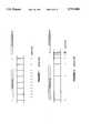
- FIGS. 3A, B and Cshow a graphical representation of the timing necessary for loading and displaying a row of pixels of a display system using a four bit weighted gray scale.
- FIGS. 3A, B and Cthere are four bits of gray scale data so that there are 16 different levels of gray.
- the graphical representation of FIG. 3Ashows time on the horizontal axis and the lines for displaying a single row of the display on its vertical axis. It will be understood that the time axis of FIG. 3A repeats for each column of the display to form a complete image in a single frame. Once the frame is displayed, the process for forming a frame repeats itself indefinitely to form each subsequent frame in a display sequence.
- the data for bit 3(the longest duration bit) for all the rows are loaded sequentially into the display.
- the datais displayed for the duration of the event as is schematically shown in FIG. 3A.
- the data for bit 2is written to the display.
- the data for bit 1is written to the display.
- the data for bit 0is written to the display.
- the data for bit 3 for the next frameis written to the display. This process of displaying the data for bit 3 must be completed within the duration of the event for bit 0.
- the sloped line 100(FIG. 3A) schematically represents the timing for loading the register with bit 3 data during the display time for event 0. It will be apparent to one of ordinary skill in the art that the bandwidth necessary to load 1280 bits of data for bit 3 of the next row during the display time for bit 0 of the present row is high.
- the frame rate for the displayis 60 Hz, i.e., the entire frame is drawn 60 times per second such that a frame is drawn in ⁇ 16.667 mSeconds. Assuming the display has 1024 rows, each row must be displayed in ⁇ 16.28 ⁇ Seconds.
- the shortest duration eventis ⁇ 64 nSeconds. This means that all 1280 bits of the next row must be written in ⁇ 64 nSeconds or ⁇ 800 pSeconds per word if loaded 16 bits at a time. This translates to ⁇ 1.25 GHz bandwidth. Naturally, these numbers are representational only. For example, the 60 Hz frame rate was drawn from standard television display technology. Other frame rates would apply for digital video signals such as produced by a high resolution computer graphics application that would typically utilize a 1280 ⁇ 1024 display.
- FIG. 3Bis a timing diagram accurately depicting the events of FIG. 3A. Rather that showing the fictional view of all events in successive rows happening simultaneously, the events for successive rows are shown actually occurring at successive cycles.
- FIG. 3Cshows graphically the bandwidth requirements for loading data into the rows for a system built according to the timing of FIG. 3B. As shown, the bandwidth requirements are high during the time that the data is transferred to the display. Accordingly, a system built according to the timing diagram of FIG. 3B will have a bandwidth requirement as described above, as prescribed by the shortest duration bit weight of the binary coding scheme. Thus, for any of the longer weighted bits, the bandwidth requirements falls to zero during significant portions of the frame time causing unwanted ⁇ dead times ⁇ . In other words, the bandwidth requirements of this system are either at a maximum level or at a zero level.
- the bandwidthcannot be reduced by simply lengthening the duration of all the events.
- an intermediate gray levelis desired. If the duration of the frame and appropriate event are sufficiently long, the displayed pixel(s) will appear to flicker rather than appear as the intermediate gray level. Thus, it is important that the display time for all of the events not be too long.
- An algorithmic time-interleaved bit-plane, pulse-width-modulation (PWM) digital display system method and apparatusreduces the bandwidth requirements necessary for providing a plurality of data entries representing multiple points of information.
- the bandwidth requirementsare constant, and for at least one system of measurement, optimal.
- a weighted PWM schememodulates an output by utilizing a frame duration that is divided into events of varying durations; most conventional schemes have each bit in the frame being half the duration of its predecessor. The modulated signal is activated during all, some or none of the events in the frame to develop a signal representing a particular parameter.
- This method and apparatuscan be used in a display for selecting among varying levels of gray scale or from among multiple colors on a palette.
- a register containing the same number of data bits as pixels in a row of the displayis provided.
- the registeris loaded, one row at a time, with one bit per column for each pixel in the entire row.
- the duration for successively display rowsis dissimilar thereby reducing the bandwidth requirements. This allows a bit for a long duration event to be displayed in one row, while bits for shorter duration events are displayed in other rows. This obviates the need to successively load the data for the shortest duration bits in all the rows.
- the organization of the sequence of the events amongst the various rowscan be arranged to achieve reduced bandwidth. If the organization is chosen in a pseudo-random manner, the order can be pre-selected for an optimized bandwidth or organized into a predetermined format to achieve an improved visual effect.
- FIG. 1shows a timing diagram for an unweighted PWM scheme in the prior art.
- FIG. 2shows a timing diagram for a weighted PWM scheme in the prior art.
- FIG. 3Ashows a timing diagram for a weighted PWM scheme viewed according to conventional consideration.
- FIG. 3Bshows the timing diagram of FIG. 3A viewed as the events actually occur in time.
- FIG. 3Cshows a bandwidth requirement diagram for a system built according to the the timing diagram of FIG. 3B.
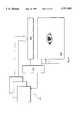
- FIG. 4shows a block diagram of an apparatus for carrying out the present invention.
- FIG. 5shows a timing diagram for a pseudo-random binary weighted PWM scheme according to one embodiment of the present invention.
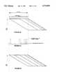
- FIG. 6Ashows a timing diagram for a weighted PWM scheme according to the preferred embodiment of the present invention.
- FIG. 6Bshows a bandwidth requirement diagram for a system built according to the the timing diagram of FIG. 6A.
- FIG. 6Cshows an alternate timing diagram for a weighted PWM scheme according to the present invention.
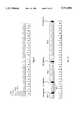
- FIG. 7Ashows a conventional timing diagram for a weighted PWM scheme.
- FIG. 7Bshows a conventional timing diagram for a weighted PWM scheme using reverse ordering from the timing shown in FIG. 7A.
- FIG. 8shows a timing diagram according to a non-binary weighted embodiment of the present invention.
- FIG. 9shows a timing diagram of the relative starting points within a time segment according to the preferred embodiment of the present invention.
- FIG. 10shows a timing diagram, including the timing for clearing data according to the present invention.
- FIG. 11shows a timing diagram for the preferred embodiment of the present invention.
- the displayis formed of an array of diffraction grating elements, such as disclosed in the Bloom, et al., U.S. Pat. No. 5,311,360, issued May 10, 1994 which is incorporated herein by reference.
- the array of diffraction grating elementsare arranged in rows and columns to form pixels of a display.
- the arraycan be formed of single grating pixels for a black and white display or time sequential multiplexing of pixels for color.
- the pixelscan be formed using multiple grating elements for each pixel to form a color display.
- light from an illumination sourcecan be made to selectively enter the display optics of display.
- the light from a pixelenters the display optics, that pixel appears lighted.
- Various levels of gray scaleare formed by lighting the pixel varying percentages of time, i.e., by modulating the pulse width.
- the preferred embodimentutilizes a weighted PWM scheme to form the gray scale selections.
- a conventional displaydraws (illuminates) one pixel at a time as it scans the beam over the entire surface of the display. Unlike conventional displays, all the pixels in a single row of the diffraction grating light valve can be updated simultaneously in the preferred embodiment. Accordingly, the descriptions of the invention that follow will be directed toward displaying a row at a time. Nevertheless, it will be apparent to one of ordinary skill in the art that the techniques of the present invention can equally be applied to other types of devices that utilize a PWM scheme for generating gray scale.
- each frameincludes 1280 ⁇ 1024 pixels for a total of 1,310,720 pixels. Assuming an 8-bit weighted gray scale, 10,485,760 data bits are required to define a single frame.
- each row of the graphical imageis formed, one row at a time. Because of the ability to draw the display, one row at a time, the number of rows multiplied by the number of bits in gray scale weighting is equal to the number of update events per frame or write cycles per frame. Thus, there are 1024 ⁇ 8 events to draw a frame. Note that an event is the transfer of pixel data from a row-wide register into a row. It will be readily understood that a number of operations (such as memory cycles) may be necessary to fill the register with the pixel data for the row.
- the row imageis displayed during one frame time such that the eight bits for each pixel in the row are appropriately presented to the viewer's eye.
- the viewer's eye/brain systemthen integrates the 8 weighted bits for each pixel into a row of pixels each of the appropriate gray scale.
- the viewer's eye/brain systemintegrates the display for each row into a single graphical image.
- the display apparatus of the present inventionincludes an image memory 400 as shown in FIG. 4.
- the image memory 400can be any convenient memory type including semiconductor memory such as RAM, including but not limited to DRAM, SRAM or VRAM, or a non-semiconductor memory such as a hard disk, floppy disk or optical disk, with or without intermediate processing (e.g., MPEG decompression).
- the image memory 400is shown in FIG. 4 as having multiple planes. This plane metaphor is used conceptually to show that each pixel includes multiple data bits for the various bits of the weighted PWM scheme; it will be apparent to those of ordinary skill in the art that any convenient organization of the graphical image data in the image memory 400 can be used.
- a control circuit 402Under control of a control circuit 402, data is transferred from the image memory 400 into a register 404. Once the register is full, and at an appropriate time according to a clock signal generated by the control circuit 402, the data in the register 404 is coupled to illuminate pixels in the appropriate row of the display 406. The display retains data of a pixel state written to the rows until they are updated in a subsequent cycle.
- the register 404contains 1280 latch and driver circuits that buffer the memory bus to the column connections of the display. As discussed in the background section of this patent document, if all 1280 latches must be loaded with data during the shortest event duration, the bandwidth requirements for the electronics becomes too severe for an economical solution.
- the present inventionre-orders the time during which the bits of the various weights are displayed in comparison to the prior art. Because the frame time is sufficiently short so that the viewer's eye/brain system can integrate the displayed image into the appropriate shades of gray, the presentation order of these bits does not affect the image quality.
- FIG. 5shows one example of an 8-bit binary weighted PWM scheme for four rows of data according to one embodiment of the present invention. As FIG. 5 clearly shows, the shortest event is not repeated in the same time slot during any of the four rows. It will be apparent to one of ordinary skill in the art after reading this disclosure that the order of the weighted bits can be selected for optimization of different characteristics, such as bandwidth or visual effect.
- FIG. 6Ashows another scheme for selecting the data to be loaded into the register without the necessity of performing a complex optimization scheme. Only the first eight rows of the row of data are shown in this Figure. Immediately before time zero, the bit in the register that corresponds to row 0 is loaded with the data for the 0th weight bit, the register bit for row 1 is loaded with the 3rd weight bit, the register for row 2 is loaded with the 2nd weight bit, the register for rows 3-6 are loaded with the 1st weight bits and row 7 is loaded with the 0th weight bit. During the next clock cycle the data in rows 1 and 2 changes such that row 1 is loaded with the data for its 0th weight bit and row 2 is loaded with the 3rd weight bit. At time one, this new data is clocked into the display. During the next clock cycle, only the data in rows 2 and 3 changes, and so forth. In this way, the number of data transitions per clock cycle is dramatically reduced and the data can be extracted from the memory in a regular fashion.
- FIG. 6Bshows a bandwidth requirement diagram for a system built according to the the timing diagram of FIG. 6A. As discussed above the bandwidth requirements of a system built according to the embodiment of FIG. 6A are reduced. Here, as shown in FIG. 6B, the bandwidth requirement becomes constant; there are no ⁇ dead times ⁇ as shown in the prior art of FIG. 3C.
- FIG. 6Cshows an alternative scheme to that of FIG. 6A. According the the scheme of FIG. 6C, the longest duration bit 602 is split into two (or more) time-separated display periods. In the example shown in FIG.
- the next shortest bit 604is displayed between the two halves of the longest duration bit 602.
- the third longest duration bit 606 and the shortest duration bit 608follow the second half of the longest duration bit 602. In this way, even if only the longest duration bit is displayed, its duty cycle is the same but the duration of each on-off cycle is sufficiently shortened to avoid forming a flicker.
- FIGS. 7A and 7Bshow the timing for loading the data for the rows of this small display according to a prior art PWM scheme.
- the time to display a frameis divided into (2 n -1) segments.
- FIG. 7Aall fifteen rows display the data for the longest event during the time segment zero. All fifteen rows display the data for the next longest event during the time segment eight. All fifteen rows display the data for the third longest event during the time segment twelve. All fifteen rows display the data for the shortest event during the time segment fourteen.
- FIG. 7Aall fifteen rows display the data for the longest event during the time segment zero. All fifteen rows display the data for the next longest event during the time segment eight. All fifteen rows display the data for the third longest event during the time segment twelve. All fifteen rows display the data for the shortest event during the time segment fourteen.
- FIG. 7Bshows the same prior art PWM timing as FIG. 7A except that the shortest event is displayed first.
- all fifteen rowsdisplay the data for the shortest event during the time segment zero.
- All fifteen rowsdisplay the data for the next shortest event during the time segment one, for the third shortest event during the time segment three and for the longest event during the time segment seven.
- FIG. 8shows the timing necessary for loading the data for the rows of this small display according to one non-binary embodiment of the present invention.
- the timing diagram for FIG. 8shows that the bandwidth requirement for the display system are considerably reduced by not having all the shortest duration events displayed at the same time.
- the time segment zerothere are four events displayed: for rows zero (the shortest event gray scale), eight (the longest event gray scale), twelve (the third shortest event) and fourteen (the second shortest event).
- the time segment one there four eventsare displayed: for rows zero (the second shortest event), one (the shortest event), nine (the longest event) and thirteen (the third shortest event).
- the time segment two only four eventsare displayed: for the rows one (the second shortest), two (the shortest), ten (the longest) and fourteen (the third shortest). This timing for displaying the rest of the frame is shown in the remainder of the drawing.
- FIG. 9shows a time chart for a single row of a display according to FIG. 8.
- the number of rows that can be drawn according to the present inventionis equal to the number of time segments. Because of the nature of conventional PWM weighting, only 2 n -1 time segments are available, where n is the number of bits of gray scale. For example, in FIG. 8, because 4 bit gray scale is used, only 15 rows can appear in the display. To provide for more rows, for example 30 rows, the timing for drawing the two halves of the array must be interleaved.
- the granularity of gray scaleis a function of the number of rows in the display or the number of rows in the video format.
- each row of bitsis first blanked before each new display event.
- FIG. 10shows a modified time chart for a single row of a display which includes these blanking times.
- the total blanking time for displaying the gray scale for a rowis equal to one time segment. Because there is one blanking time of duration 1/n for each bit of gray scale one full time segment is added.
- the preferred embodimentincludes 2 n time segments rather than 2 n -1 as found in the prior art. Accordingly, this embodiment can readily support drawing sixteen rows as shown in FIG. 11 rather than the fifteen rows shown in FIGS. 7A, 7B and 8. Referring now to FIG. 10, the timing can be seen for a single row having its shortest event first.
- Bit zero(the shortest event) is displayed during the first time segment. Next, the blanking period is provided for bit 1 for a duration of 1/4 time segment. Then, bit 1 is displayed for a total period of 2 time segments. This sequence continues for the remaining bits of gray scale control.
- FIGS. 7A, 7B, 8 and 11imply that the rows of an entire frame image are all simultaneously displayed.
- the data for each frameis received serially.
- FIG. 6shows a time line representation for the timing of data presentation of the rows in a display.
- the shaded portion 600 of FIG. 6shows the collection of data and their respective timing for forming a single frame image. As the first row of a new frame image is drawn onto the display, the remaining portion of the previous frame image is still being displayed.
- Table Ishows the timing for displaying the lowest order bit according to the scheme of FIG. 7B. According to Table I, each data bit is sequentially loaded into each row as also shown in FIG. 3. To display a frame, 240 clock cycles are needed for 4 bit gray scale according to one version of the prior art.
- Table IIshows the timing of the present invention.
- the timing for loading and for clearing the datais indicated such as graphically indicated in FIG. 10.
- the data for Bit0, Row0is loaded and data for Row15 is cleared.
- the data for Bit1, Row15is loaded and data for row 13 is cleared.
- This analysiscontinues for the remainder of Table II.
- 64 clock cyclesare needed for 4 bit gray scale according to the preferred embodiment of the present invention.
- Virtual linescan be added to the display sequence to match the gray scale resolution requirement. It will be understood that these virtual rows are not display but rather add only to the sequence of events for forming the display image. For example, if only 480 lines comprise a frame, and the cycle time is adjusted to represent 512 lines per frame, the a 6% increase in bandwidth results. In this case 6% of the possible update cycles are not used for writing data to the display.
- a second approach for resolving a non-matching gray scale-display systemis to use the granularity provided by the total number of rows.
- the gray scale definitioncan be reduced and/or a higher bandwidth can be implemented.
- a 480 row displaywould achieve nearly 9 bits of gray scale resolution (512 levels), but some of the binary codes would be missing while others would produce equal output brightness.
- 9 bits of gray scaleare used to encode the 480 distinct values, a 12% increase in bandwidth results.
- a third approach for resolving a non-matching gray scale-display systemis to increase the duration of the least significant bits in combination with a clear behind technique such as taught in U.S. patent application, Ser. No. 08/482,192, filed Jun. 7, 1995, and entitled CLEAR-BEHIND MATRIX ADDRESSING FOR DISPLAY SYSTEMS.
- Such a systemcan provide a bandwidth optimal system for a non-power-of-2 number of rows but reduces the optical efficiency.
Landscapes
- Engineering & Computer Science (AREA)
- Physics & Mathematics (AREA)
- Computer Hardware Design (AREA)
- General Physics & Mathematics (AREA)
- Theoretical Computer Science (AREA)
- Control Of Indicators Other Than Cathode Ray Tubes (AREA)
- Controls And Circuits For Display Device (AREA)
- Liquid Crystal Display Device Control (AREA)
- Radar Systems Or Details Thereof (AREA)
- Liquid Crystal (AREA)
- Transmission Systems Not Characterized By The Medium Used For Transmission (AREA)
Abstract
Description
TABLE I ______________________________________ time row bit ______________________________________ t1 r1 b0 t2 r2 b0 t3 r3 b0 t4 r4 b0 t5 r5 b0 t6 r6 b0 t7 r7 b0 t8 r8 b0 t9 r9 b0 t10 r10 b0 t11 r11 b0 t12 r12 b0 t13 r13 b0 t14 r14 b0 t15 r15 b0 t16 r16 b0 t17 r1 b1 . . . . . . . . . ______________________________________
TABLE II ______________________________________ time row bit clear ______________________________________ t1 r0 b0 r15 t2 r15 b1 r13 t3 r13 b2 r9 t4 r9 b3 r1 t5 r1 b0 r0 t6 r0 b1 r14 t7 r14 b2 r10 t8 r10 b3 r2 t9 r2 b0 r1 t10 r1 b1 r15 t11 r15 b2 r11 t12 r11 b3 r3 t13 r3 b0 r2 t14 r2 b1 r0 t15 r0 b2 r12 t16 r12 b3 r4 ______________________________________
Claims (27)
Priority Applications (9)
| Application Number | Priority Date | Filing Date | Title |
|---|---|---|---|
| US08/635,479US5731802A (en) | 1996-04-22 | 1996-04-22 | Time-interleaved bit-plane, pulse-width-modulation digital display system |
| EP97921309AEP0897573B1 (en) | 1996-04-22 | 1997-04-21 | Time-interleaved bit-plane, pulse-width-modulation digital display system |
| KR1019980708440AKR20000010572A (en) | 1996-04-22 | 1997-04-21 | Time-interleaved bit-plane, pulse width modulation digital display system |
| AU27380/97AAU2738097A (en) | 1996-04-22 | 1997-04-21 | Time-interleaved bit-plane, pulse-width-modulation digital display system |
| JP09538252AJP2000510252A (en) | 1996-04-22 | 1997-04-21 | Time, interleave, bit, plane pulse width, modulation digital display system |
| AT97921309TATE225071T1 (en) | 1996-04-22 | 1997-04-21 | DIGITAL DISPLAY SYSTEM WITH TIME INTERESTED BIT PLANE AND PULSE WIDTH MODULATION |
| PCT/US1997/006656WO1997040487A1 (en) | 1996-04-22 | 1997-04-21 | Time-interleaved bit-plane, pulse-width-modulation digital display system |
| DE69715837TDE69715837T2 (en) | 1996-04-22 | 1997-04-21 | DIGITAL DISPLAY SYSTEM WITH TIME INTERLOCKED BIT LEVEL AND PULSE WIDTH MODULATION |
| NO984907ANO984907L (en) | 1996-04-22 | 1998-10-21 | Digital display system with timed bit plane pulse width modulation |
Applications Claiming Priority (1)
| Application Number | Priority Date | Filing Date | Title |
|---|---|---|---|
| US08/635,479US5731802A (en) | 1996-04-22 | 1996-04-22 | Time-interleaved bit-plane, pulse-width-modulation digital display system |
Publications (1)
| Publication Number | Publication Date |
|---|---|
| US5731802Atrue US5731802A (en) | 1998-03-24 |
Family
ID=24547954
Family Applications (1)
| Application Number | Title | Priority Date | Filing Date |
|---|---|---|---|
| US08/635,479Expired - Fee RelatedUS5731802A (en) | 1996-04-22 | 1996-04-22 | Time-interleaved bit-plane, pulse-width-modulation digital display system |
Country Status (9)
| Country | Link |
|---|---|
| US (1) | US5731802A (en) |
| EP (1) | EP0897573B1 (en) |
| JP (1) | JP2000510252A (en) |
| KR (1) | KR20000010572A (en) |
| AT (1) | ATE225071T1 (en) |
| AU (1) | AU2738097A (en) |
| DE (1) | DE69715837T2 (en) |
| NO (1) | NO984907L (en) |
| WO (1) | WO1997040487A1 (en) |
Cited By (132)
| Publication number | Priority date | Publication date | Assignee | Title |
|---|---|---|---|---|
| US6052112A (en)* | 1996-10-23 | 2000-04-18 | Nec Corporation | Gradation display system |
| US6100863A (en)* | 1998-03-31 | 2000-08-08 | Matsushita Electric Industrial Co., Ltd. | Motion pixel distortion reduction for digital display devices using dynamic programming coding |
| US6151001A (en)* | 1998-01-30 | 2000-11-21 | Electro Plasma, Inc. | Method and apparatus for minimizing false image artifacts in a digitally controlled display monitor |
| US6151011A (en)* | 1998-02-27 | 2000-11-21 | Aurora Systems, Inc. | System and method for using compound data words to reduce the data phase difference between adjacent pixel electrodes |
| WO2001054112A1 (en)* | 2000-01-18 | 2001-07-26 | Aurora Systems, Inc. | System and method for using compound data words in a field sequential display driving scheme |
| US6268838B1 (en)* | 1996-07-02 | 2001-07-31 | Lg Electronics Inc. | Method and circuit for driving PDP |
| WO2001084531A1 (en)* | 2000-05-03 | 2001-11-08 | Reflectivity, Inc. | Monochrome and color digital display systems and methods for implementing the same |
| US6323833B1 (en)* | 1997-03-24 | 2001-11-27 | Ngk Insulators, Ltd. | Optical waveguide display with movable actuators which cause light leakage in waveguide at each display elements to provide gradation in a display image by temporal subfield modulation |
| US6452583B1 (en)* | 1997-07-18 | 2002-09-17 | Ngk Insulators, Ltd. | Display-driving device and display-driving method |
| US20020154083A1 (en)* | 2001-04-19 | 2002-10-24 | Toshio Miyazawa | Display device and method of driving same |
| US6501600B1 (en) | 1999-08-11 | 2002-12-31 | Lightconnect, Inc. | Polarization independent grating modulator |
| US20030156128A1 (en)* | 2002-02-21 | 2003-08-21 | Seiko Epson Corporation | Driving method for electro-optical device, driving circuit therefor, electro-optical device, and electronic apparatus |
| US20030206185A1 (en)* | 2002-05-04 | 2003-11-06 | Cedric Thebault | Multiscan display on a plasma display panel |
| US6674563B2 (en) | 2000-04-13 | 2004-01-06 | Lightconnect, Inc. | Method and apparatus for device linearization |
| US6690499B1 (en)* | 2000-11-22 | 2004-02-10 | Displaytech, Inc. | Multi-state light modulator with non-zero response time and linear gray scale |
| US20040036707A1 (en)* | 2002-08-21 | 2004-02-26 | Willis Thomas E | Pulse width modulated spatial light modulators with offset pulses |
| US6707591B2 (en) | 2001-04-10 | 2004-03-16 | Silicon Light Machines | Angled illumination for a single order light modulator based projection system |
| US6712480B1 (en) | 2002-09-27 | 2004-03-30 | Silicon Light Machines | Controlled curvature of stressed micro-structures |
| US6714337B1 (en) | 2002-06-28 | 2004-03-30 | Silicon Light Machines | Method and device for modulating a light beam and having an improved gamma response |
| US6728023B1 (en) | 2002-05-28 | 2004-04-27 | Silicon Light Machines | Optical device arrays with optimized image resolution |
| US6747781B2 (en) | 2001-06-25 | 2004-06-08 | Silicon Light Machines, Inc. | Method, apparatus, and diffuser for reducing laser speckle |
| US20040135927A1 (en)* | 2001-03-14 | 2004-07-15 | Udo Fischbeck | Method and device for improving the grey scale resolution of a pulse width modulated image display device |
| US6764875B2 (en) | 1998-07-29 | 2004-07-20 | Silicon Light Machines | Method of and apparatus for sealing an hermetic lid to a semiconductor die |
| US6767751B2 (en) | 2002-05-28 | 2004-07-27 | Silicon Light Machines, Inc. | Integrated driver process flow |
| US6782205B2 (en) | 2001-06-25 | 2004-08-24 | Silicon Light Machines | Method and apparatus for dynamic equalization in wavelength division multiplexing |
| US6800238B1 (en) | 2002-01-15 | 2004-10-05 | Silicon Light Machines, Inc. | Method for domain patterning in low coercive field ferroelectrics |
| US6801354B1 (en) | 2002-08-20 | 2004-10-05 | Silicon Light Machines, Inc. | 2-D diffraction grating for substantially eliminating polarization dependent losses |
| US6806997B1 (en) | 2003-02-28 | 2004-10-19 | Silicon Light Machines, Inc. | Patterned diffractive light modulator ribbon for PDL reduction |
| US6813059B2 (en) | 2002-06-28 | 2004-11-02 | Silicon Light Machines, Inc. | Reduced formation of asperities in contact micro-structures |
| US6822797B1 (en) | 2002-05-31 | 2004-11-23 | Silicon Light Machines, Inc. | Light modulator structure for producing high-contrast operation using zero-order light |
| US6826330B1 (en) | 1999-08-11 | 2004-11-30 | Lightconnect, Inc. | Dynamic spectral shaping for fiber-optic application |
| US6829077B1 (en) | 2003-02-28 | 2004-12-07 | Silicon Light Machines, Inc. | Diffractive light modulator with dynamically rotatable diffraction plane |
| US6829258B1 (en) | 2002-06-26 | 2004-12-07 | Silicon Light Machines, Inc. | Rapidly tunable external cavity laser |
| US6829092B2 (en) | 2001-08-15 | 2004-12-07 | Silicon Light Machines, Inc. | Blazed grating light valve |
| US6865346B1 (en) | 2001-06-05 | 2005-03-08 | Silicon Light Machines Corporation | Fiber optic transceiver |
| US20050062765A1 (en)* | 2003-09-23 | 2005-03-24 | Elcos Microdisplay Technology, Inc. | Temporally dispersed modulation method |
| US6872984B1 (en) | 1998-07-29 | 2005-03-29 | Silicon Light Machines Corporation | Method of sealing a hermetic lid to a semiconductor die at an angle |
| US6888983B2 (en) | 2000-04-14 | 2005-05-03 | Lightconnect, Inc. | Dynamic gain and channel equalizers |
| US20050128223A1 (en)* | 2003-12-12 | 2005-06-16 | Adam Ghozeil | Method and system for generating pixel gray scale levels |
| US6908201B2 (en) | 2002-06-28 | 2005-06-21 | Silicon Light Machines Corporation | Micro-support structures |
| US6922273B1 (en) | 2003-02-28 | 2005-07-26 | Silicon Light Machines Corporation | PDL mitigation structure for diffractive MEMS and gratings |
| US6922272B1 (en) | 2003-02-14 | 2005-07-26 | Silicon Light Machines Corporation | Method and apparatus for leveling thermal stress variations in multi-layer MEMS devices |
| US6928207B1 (en) | 2002-12-12 | 2005-08-09 | Silicon Light Machines Corporation | Apparatus for selectively blocking WDM channels |
| US6927891B1 (en) | 2002-12-23 | 2005-08-09 | Silicon Light Machines Corporation | Tilt-able grating plane for improved crosstalk in 1×N blaze switches |
| US6934070B1 (en) | 2002-12-18 | 2005-08-23 | Silicon Light Machines Corporation | Chirped optical MEM device |
| US6947613B1 (en) | 2003-02-11 | 2005-09-20 | Silicon Light Machines Corporation | Wavelength selective switch and equalizer |
| US6956878B1 (en) | 2000-02-07 | 2005-10-18 | Silicon Light Machines Corporation | Method and apparatus for reducing laser speckle using polarization averaging |
| US6956995B1 (en) | 2001-11-09 | 2005-10-18 | Silicon Light Machines Corporation | Optical communication arrangement |
| US20050275643A1 (en)* | 2004-06-11 | 2005-12-15 | Peter Richards | Asymmetrical switching delay compensation in display systems |
| US6987600B1 (en) | 2002-12-17 | 2006-01-17 | Silicon Light Machines Corporation | Arbitrary phase profile for better equalization in dynamic gain equalizer |
| US6991953B1 (en) | 2001-09-13 | 2006-01-31 | Silicon Light Machines Corporation | Microelectronic mechanical system and methods |
| US7027202B1 (en) | 2003-02-28 | 2006-04-11 | Silicon Light Machines Corp | Silicon substrate as a light modulator sacrificial layer |
| US7042611B1 (en) | 2003-03-03 | 2006-05-09 | Silicon Light Machines Corporation | Pre-deflected bias ribbons |
| US7054515B1 (en) | 2002-05-30 | 2006-05-30 | Silicon Light Machines Corporation | Diffractive light modulator-based dynamic equalizer with integrated spectral monitor |
| US7057819B1 (en) | 2002-12-17 | 2006-06-06 | Silicon Light Machines Corporation | High contrast tilting ribbon blazed grating |
| US7057795B2 (en) | 2002-08-20 | 2006-06-06 | Silicon Light Machines Corporation | Micro-structures with individually addressable ribbon pairs |
| US20060132405A1 (en)* | 2004-12-22 | 2006-06-22 | Shwang-Shi Bai | Frame-varying addressing method of color sequential display |
| US7068372B1 (en) | 2003-01-28 | 2006-06-27 | Silicon Light Machines Corporation | MEMS interferometer-based reconfigurable optical add-and-drop multiplexor |
| US20060164443A1 (en)* | 2005-01-26 | 2006-07-27 | Kettle Wiatt E | Modulating spatial light modulator with logically OR'ed values of bit planes |
| US20060187531A1 (en)* | 2005-02-23 | 2006-08-24 | Pixtronix, Incorporated | Methods and apparatus for bi-stable actuation of displays |
| US20060187190A1 (en)* | 2005-02-23 | 2006-08-24 | Pixtronix, Incorporated | Display methods and apparatus |
| US20060187191A1 (en)* | 2005-02-23 | 2006-08-24 | Pixtronix, Incorporated | Display methods and apparatus |
| US20060187528A1 (en)* | 2005-02-23 | 2006-08-24 | Pixtronix, Incorporated | Methods and apparatus for spatial light modulation |
| US20060209012A1 (en)* | 2005-02-23 | 2006-09-21 | Pixtronix, Incorporated | Devices having MEMS displays |
| US20060250676A1 (en)* | 2005-02-23 | 2006-11-09 | Pixtronix, Incorporated | Light concentrating reflective display methods and apparatus |
| US20060256039A1 (en)* | 2005-02-23 | 2006-11-16 | Pixtronix, Incorporated | Display methods and apparatus |
| US20060284900A1 (en)* | 2005-06-16 | 2006-12-21 | Ng Sunny Y | Single pulse display driving scheme and display |
| US20070002156A1 (en)* | 2005-02-23 | 2007-01-04 | Pixtronix, Incorporated | Display apparatus and methods for manufacture thereof |
| US7177081B2 (en) | 2001-03-08 | 2007-02-13 | Silicon Light Machines Corporation | High contrast grating light valve type device |
| US7271945B2 (en) | 2005-02-23 | 2007-09-18 | Pixtronix, Inc. | Methods and apparatus for actuating displays |
| US7286764B1 (en) | 2003-02-03 | 2007-10-23 | Silicon Light Machines Corporation | Reconfigurable modulator-based optical add-and-drop multiplexer |
| US7304785B2 (en) | 2005-02-23 | 2007-12-04 | Pixtronix, Inc. | Display methods and apparatus |
| US20070279727A1 (en)* | 2006-06-05 | 2007-12-06 | Pixtronix, Inc. | Display apparatus with optical cavities |
| US20070279324A1 (en)* | 2003-12-17 | 2007-12-06 | Sebastien Weitbruch | Method And Apparatus For Processing Video Pictures, In Particular In Film Mode Sequences |
| US20080074409A1 (en)* | 2004-09-09 | 2008-03-27 | Erhard Lehmann | Method for Controlling the Power Supply from a Power Source to a Power Consumer |
| US7391973B1 (en) | 2003-02-28 | 2008-06-24 | Silicon Light Machines Corporation | Two-stage gain equalizer |
| US7403213B1 (en)* | 1997-06-04 | 2008-07-22 | Texas Instruments Incorporated | Boundary dispersion for artifact mitigation |
| US20080201665A1 (en)* | 2007-02-15 | 2008-08-21 | Teac Corporation | Electronic equipment having plural function keys |
| US20080259019A1 (en)* | 2005-06-16 | 2008-10-23 | Ng Sunny Yat-San | Asynchronous display driving scheme and display |
| US20090027363A1 (en)* | 2007-07-27 | 2009-01-29 | Kin Yip Kenneth Kwan | Display device and driving method using multiple pixel control units |
| US7502159B2 (en) | 2005-02-23 | 2009-03-10 | Pixtronix, Inc. | Methods and apparatus for actuating displays |
| US20090257245A1 (en)* | 2008-04-18 | 2009-10-15 | Pixtronix, Inc. | Light guides and backlight systems incorporating prismatic structures and light redirectors |
| US20090303248A1 (en)* | 2008-06-06 | 2009-12-10 | Ng Sunny Yat-San | System and method for dithering video data |
| US20090303206A1 (en)* | 2008-06-06 | 2009-12-10 | Ng Sunny Yat-San | Data dependent drive scheme and display |
| US7675665B2 (en) | 2005-02-23 | 2010-03-09 | Pixtronix, Incorporated | Methods and apparatus for actuating displays |
| US7746529B2 (en) | 2005-02-23 | 2010-06-29 | Pixtronix, Inc. | MEMS display apparatus |
| US20100188443A1 (en)* | 2007-01-19 | 2010-07-29 | Pixtronix, Inc | Sensor-based feedback for display apparatus |
| US7839356B2 (en) | 2005-02-23 | 2010-11-23 | Pixtronix, Incorporated | Display methods and apparatus |
| US7852546B2 (en) | 2007-10-19 | 2010-12-14 | Pixtronix, Inc. | Spacers for maintaining display apparatus alignment |
| US20110148948A1 (en)* | 2005-02-23 | 2011-06-23 | Pixtronix, Inc. | Circuits for controlling display apparatus |
| US20110157679A1 (en)* | 2008-08-04 | 2011-06-30 | Pixtronix, Inc. | Methods for manufacturing cold seal fluid-filled display apparatus |
| US20110205756A1 (en)* | 2010-02-19 | 2011-08-25 | Pixtronix, Inc. | Light guides and backlight systems incorporating prismatic structures and light redirectors |
| US20110205259A1 (en)* | 2008-10-28 | 2011-08-25 | Pixtronix, Inc. | System and method for selecting display modes |
| US8228350B2 (en) | 2008-06-06 | 2012-07-24 | Omnivision Technologies, Inc. | Data dependent drive scheme and display |
| US8262274B2 (en) | 2006-10-20 | 2012-09-11 | Pitronix, Inc. | Light guides and backlight systems incorporating light redirectors at varying densities |
| US8310442B2 (en) | 2005-02-23 | 2012-11-13 | Pixtronix, Inc. | Circuits for controlling display apparatus |
| US8482496B2 (en) | 2006-01-06 | 2013-07-09 | Pixtronix, Inc. | Circuits for controlling MEMS display apparatus on a transparent substrate |
| US8519945B2 (en) | 2006-01-06 | 2013-08-27 | Pixtronix, Inc. | Circuits for controlling display apparatus |
| US8526096B2 (en) | 2006-02-23 | 2013-09-03 | Pixtronix, Inc. | Mechanical light modulators with stressed beams |
| US8599463B2 (en) | 2008-10-27 | 2013-12-03 | Pixtronix, Inc. | MEMS anchors |
| US8749538B2 (en) | 2011-10-21 | 2014-06-10 | Qualcomm Mems Technologies, Inc. | Device and method of controlling brightness of a display based on ambient lighting conditions |
| US9082353B2 (en) | 2010-01-05 | 2015-07-14 | Pixtronix, Inc. | Circuits for controlling display apparatus |
| US9134552B2 (en) | 2013-03-13 | 2015-09-15 | Pixtronix, Inc. | Display apparatus with narrow gap electrostatic actuators |
| US9135868B2 (en) | 2005-02-23 | 2015-09-15 | Pixtronix, Inc. | Direct-view MEMS display devices and methods for generating images thereon |
| US9176318B2 (en) | 2007-05-18 | 2015-11-03 | Pixtronix, Inc. | Methods for manufacturing fluid-filled MEMS displays |
| US9183812B2 (en) | 2013-01-29 | 2015-11-10 | Pixtronix, Inc. | Ambient light aware display apparatus |
| US9229222B2 (en) | 2005-02-23 | 2016-01-05 | Pixtronix, Inc. | Alignment methods in fluid-filled MEMS displays |
| US9261694B2 (en) | 2005-02-23 | 2016-02-16 | Pixtronix, Inc. | Display apparatus and methods for manufacture thereof |
| US20160077367A1 (en)* | 2014-05-14 | 2016-03-17 | Jasper Display Corp. | System And Method For Pulse-Width Modulating A Phase-Only Spatial Light Modulator |
| US9398666B2 (en) | 2010-03-11 | 2016-07-19 | Pixtronix, Inc. | Reflective and transflective operation modes for a display device |
| US9500853B2 (en) | 2005-02-23 | 2016-11-22 | Snaptrack, Inc. | MEMS-based display apparatus |
| US9640108B2 (en) | 2015-08-25 | 2017-05-02 | X-Celeprint Limited | Bit-plane pulse width modulated digital display system |
| US9930277B2 (en) | 2015-12-23 | 2018-03-27 | X-Celeprint Limited | Serial row-select matrix-addressed system |
| US9928771B2 (en) | 2015-12-24 | 2018-03-27 | X-Celeprint Limited | Distributed pulse width modulation control |
| US20180197471A1 (en)* | 2017-01-10 | 2018-07-12 | X-Celeprint Limited | Digital-drive pulse-width-modulated output system |
| US10091446B2 (en) | 2015-12-23 | 2018-10-02 | X-Celeprint Limited | Active-matrix displays with common pixel control |
| US10360846B2 (en) | 2016-05-10 | 2019-07-23 | X-Celeprint Limited | Distributed pulse-width modulation system with multi-bit digital storage and output device |
| US10453826B2 (en) | 2016-06-03 | 2019-10-22 | X-Celeprint Limited | Voltage-balanced serial iLED pixel and display |
| US20220114976A1 (en)* | 2020-10-08 | 2022-04-14 | Samsung Electronics Co., Ltd. | Electronic apparatus and control method thereof |
| US11538431B2 (en) | 2020-06-29 | 2022-12-27 | Google Llc | Larger backplane suitable for high speed applications |
| US11568802B2 (en) | 2017-10-13 | 2023-01-31 | Google Llc | Backplane adaptable to drive emissive pixel arrays of differing pitches |
| US11615736B2 (en)* | 2020-09-09 | 2023-03-28 | Texas Instruments Incorporated | Light-emitting diode (LED) display driver with blank time distribution |
| US11626062B2 (en) | 2020-02-18 | 2023-04-11 | Google Llc | System and method for modulating an array of emissive elements |
| US11637219B2 (en) | 2019-04-12 | 2023-04-25 | Google Llc | Monolithic integration of different light emitting structures on a same substrate |
| US11710445B2 (en) | 2019-01-24 | 2023-07-25 | Google Llc | Backplane configurations and operations |
| US11810509B2 (en) | 2021-07-14 | 2023-11-07 | Google Llc | Backplane and method for pulse width modulation |
| US11847957B2 (en) | 2019-06-28 | 2023-12-19 | Google Llc | Backplane for an array of emissive elements |
| US11961431B2 (en) | 2018-07-03 | 2024-04-16 | Google Llc | Display processing circuitry |
| US12039913B2 (en)* | 2018-07-05 | 2024-07-16 | Boe Technology Group Co., Ltd. | Pixel circuit, driving method thereof, and display panel |
| US12107072B2 (en) | 2020-04-06 | 2024-10-01 | Google Llc | Display backplane including an array of tiles |
| US12244786B2 (en) | 2020-12-21 | 2025-03-04 | Google Llc | High density pixel arrays for auto-viewed 3D displays |
| US20250316208A1 (en)* | 2024-04-03 | 2025-10-09 | Omnivision Technologies, Inc. | Method to implement global dimming for microled display |
Families Citing this family (3)
| Publication number | Priority date | Publication date | Assignee | Title |
|---|---|---|---|---|
| US20200357348A1 (en)* | 2016-04-28 | 2020-11-12 | Sony Corporation | Image display apparatus and image display method |
| CN109891485B (en) | 2016-10-27 | 2022-08-16 | 索尼公司 | Display device |
| DE102019113916A1 (en) | 2019-05-24 | 2020-11-26 | OSRAM Opto Semiconductors Gesellschaft mit beschränkter Haftung | Optoelectronic lighting device with a programming device and method for controlling an optoelectronic lighting device |
Citations (7)
| Publication number | Priority date | Publication date | Assignee | Title |
|---|---|---|---|---|
| US4021607A (en)* | 1973-05-19 | 1977-05-03 | Sony Corporation | Video display system employing drive pulse of variable amplitude and width |
| US5185602A (en)* | 1989-04-10 | 1993-02-09 | Cirrus Logic, Inc. | Method and apparatus for producing perception of high quality grayscale shading on digitally commanded displays |
| US5196839A (en)* | 1988-09-16 | 1993-03-23 | Chips And Technologies, Inc. | Gray scales method and circuitry for flat panel graphics display |
| US5497172A (en)* | 1994-06-13 | 1996-03-05 | Texas Instruments Incorporated | Pulse width modulation for spatial light modulator with split reset addressing |
| US5523803A (en)* | 1991-04-01 | 1996-06-04 | Texas Instruments Incorporated | DMD architecture and timing for use in a pulse-width modulated display system |
| US5548301A (en)* | 1993-01-11 | 1996-08-20 | Texas Instruments Incorporated | Pixel control circuitry for spatial light modulator |
| US5619224A (en)* | 1993-12-28 | 1997-04-08 | Seiko Instruments Inc. | Liquid crystal display panel driving device |
Family Cites Families (3)
| Publication number | Priority date | Publication date | Assignee | Title |
|---|---|---|---|---|
| JP2932686B2 (en)* | 1990-11-28 | 1999-08-09 | 日本電気株式会社 | Driving method of plasma display panel |
| WO1994009473A1 (en)* | 1992-10-15 | 1994-04-28 | Rank Brimar Limited | Display device |
| EP0685830A1 (en)* | 1994-06-02 | 1995-12-06 | Texas Instruments Incorporated | Improvements in or relating to spatial light modulators |
- 1996
- 1996-04-22USUS08/635,479patent/US5731802A/ennot_activeExpired - Fee Related
- 1997
- 1997-04-21WOPCT/US1997/006656patent/WO1997040487A1/enactiveIP Right Grant
- 1997-04-21KRKR1019980708440Apatent/KR20000010572A/ennot_activeAbandoned
- 1997-04-21EPEP97921309Apatent/EP0897573B1/ennot_activeExpired - Lifetime
- 1997-04-21ATAT97921309Tpatent/ATE225071T1/ennot_activeIP Right Cessation
- 1997-04-21JPJP09538252Apatent/JP2000510252A/enactivePending
- 1997-04-21AUAU27380/97Apatent/AU2738097A/ennot_activeAbandoned
- 1997-04-21DEDE69715837Tpatent/DE69715837T2/ennot_activeExpired - Fee Related
- 1998
- 1998-10-21NONO984907Apatent/NO984907L/ennot_activeApplication Discontinuation
Patent Citations (8)
| Publication number | Priority date | Publication date | Assignee | Title |
|---|---|---|---|---|
| US4021607A (en)* | 1973-05-19 | 1977-05-03 | Sony Corporation | Video display system employing drive pulse of variable amplitude and width |
| US5196839A (en)* | 1988-09-16 | 1993-03-23 | Chips And Technologies, Inc. | Gray scales method and circuitry for flat panel graphics display |
| US5185602A (en)* | 1989-04-10 | 1993-02-09 | Cirrus Logic, Inc. | Method and apparatus for producing perception of high quality grayscale shading on digitally commanded displays |
| US5293159A (en)* | 1989-04-10 | 1994-03-08 | Cirrus Logic, Inc. | Method and apparatus for producing perception of high quality grayscale shading on digitally commanded displays |
| US5523803A (en)* | 1991-04-01 | 1996-06-04 | Texas Instruments Incorporated | DMD architecture and timing for use in a pulse-width modulated display system |
| US5548301A (en)* | 1993-01-11 | 1996-08-20 | Texas Instruments Incorporated | Pixel control circuitry for spatial light modulator |
| US5619224A (en)* | 1993-12-28 | 1997-04-08 | Seiko Instruments Inc. | Liquid crystal display panel driving device |
| US5497172A (en)* | 1994-06-13 | 1996-03-05 | Texas Instruments Incorporated | Pulse width modulation for spatial light modulator with split reset addressing |
Cited By (210)
| Publication number | Priority date | Publication date | Assignee | Title |
|---|---|---|---|---|
| US6268838B1 (en)* | 1996-07-02 | 2001-07-31 | Lg Electronics Inc. | Method and circuit for driving PDP |
| US6052112A (en)* | 1996-10-23 | 2000-04-18 | Nec Corporation | Gradation display system |
| US6323833B1 (en)* | 1997-03-24 | 2001-11-27 | Ngk Insulators, Ltd. | Optical waveguide display with movable actuators which cause light leakage in waveguide at each display elements to provide gradation in a display image by temporal subfield modulation |
| US20090021540A1 (en)* | 1997-06-04 | 2009-01-22 | Texas Instruments Incorporated | Boundary Dispersion for Mitigating PWM Temporal Contouring Artifacts in Digital Displays |
| US8717394B2 (en) | 1997-06-04 | 2014-05-06 | Texas Instruments Incorporated | Boundary dispersion for mitigating PWM temporal contouring artifacts in digital displays |
| US7403213B1 (en)* | 1997-06-04 | 2008-07-22 | Texas Instruments Incorporated | Boundary dispersion for artifact mitigation |
| US6452583B1 (en)* | 1997-07-18 | 2002-09-17 | Ngk Insulators, Ltd. | Display-driving device and display-driving method |
| US6151001A (en)* | 1998-01-30 | 2000-11-21 | Electro Plasma, Inc. | Method and apparatus for minimizing false image artifacts in a digitally controlled display monitor |
| US6151011A (en)* | 1998-02-27 | 2000-11-21 | Aurora Systems, Inc. | System and method for using compound data words to reduce the data phase difference between adjacent pixel electrodes |
| US6326980B1 (en)* | 1998-02-27 | 2001-12-04 | Aurora Systems, Inc. | System and method for using compound data words in a field sequential display driving scheme |
| US6100863A (en)* | 1998-03-31 | 2000-08-08 | Matsushita Electric Industrial Co., Ltd. | Motion pixel distortion reduction for digital display devices using dynamic programming coding |
| US6764875B2 (en) | 1998-07-29 | 2004-07-20 | Silicon Light Machines | Method of and apparatus for sealing an hermetic lid to a semiconductor die |
| US6872984B1 (en) | 1998-07-29 | 2005-03-29 | Silicon Light Machines Corporation | Method of sealing a hermetic lid to a semiconductor die at an angle |
| US6826330B1 (en) | 1999-08-11 | 2004-11-30 | Lightconnect, Inc. | Dynamic spectral shaping for fiber-optic application |
| US6501600B1 (en) | 1999-08-11 | 2002-12-31 | Lightconnect, Inc. | Polarization independent grating modulator |
| WO2001054112A1 (en)* | 2000-01-18 | 2001-07-26 | Aurora Systems, Inc. | System and method for using compound data words in a field sequential display driving scheme |
| US6956878B1 (en) | 2000-02-07 | 2005-10-18 | Silicon Light Machines Corporation | Method and apparatus for reducing laser speckle using polarization averaging |
| US6674563B2 (en) | 2000-04-13 | 2004-01-06 | Lightconnect, Inc. | Method and apparatus for device linearization |
| US6888983B2 (en) | 2000-04-14 | 2005-05-03 | Lightconnect, Inc. | Dynamic gain and channel equalizers |
| WO2001084531A1 (en)* | 2000-05-03 | 2001-11-08 | Reflectivity, Inc. | Monochrome and color digital display systems and methods for implementing the same |
| US6388661B1 (en)* | 2000-05-03 | 2002-05-14 | Reflectivity, Inc. | Monochrome and color digital display systems and methods |
| US6756976B2 (en) | 2000-05-03 | 2004-06-29 | Reflectivity, Inc | Monochrome and color digital display systems and methods for implementing the same |
| US6690499B1 (en)* | 2000-11-22 | 2004-02-10 | Displaytech, Inc. | Multi-state light modulator with non-zero response time and linear gray scale |
| US7177081B2 (en) | 2001-03-08 | 2007-02-13 | Silicon Light Machines Corporation | High contrast grating light valve type device |
| US20040135927A1 (en)* | 2001-03-14 | 2004-07-15 | Udo Fischbeck | Method and device for improving the grey scale resolution of a pulse width modulated image display device |
| US6707591B2 (en) | 2001-04-10 | 2004-03-16 | Silicon Light Machines | Angled illumination for a single order light modulator based projection system |
| US7042429B2 (en)* | 2001-04-19 | 2006-05-09 | Hitachi, Ltd. | Display device and method of driving same |
| US20020154083A1 (en)* | 2001-04-19 | 2002-10-24 | Toshio Miyazawa | Display device and method of driving same |
| US6865346B1 (en) | 2001-06-05 | 2005-03-08 | Silicon Light Machines Corporation | Fiber optic transceiver |
| US6747781B2 (en) | 2001-06-25 | 2004-06-08 | Silicon Light Machines, Inc. | Method, apparatus, and diffuser for reducing laser speckle |
| US6782205B2 (en) | 2001-06-25 | 2004-08-24 | Silicon Light Machines | Method and apparatus for dynamic equalization in wavelength division multiplexing |
| US6829092B2 (en) | 2001-08-15 | 2004-12-07 | Silicon Light Machines, Inc. | Blazed grating light valve |
| US6991953B1 (en) | 2001-09-13 | 2006-01-31 | Silicon Light Machines Corporation | Microelectronic mechanical system and methods |
| US7049164B2 (en) | 2001-09-13 | 2006-05-23 | Silicon Light Machines Corporation | Microelectronic mechanical system and methods |
| US6956995B1 (en) | 2001-11-09 | 2005-10-18 | Silicon Light Machines Corporation | Optical communication arrangement |
| US6800238B1 (en) | 2002-01-15 | 2004-10-05 | Silicon Light Machines, Inc. | Method for domain patterning in low coercive field ferroelectrics |
| US20030156128A1 (en)* | 2002-02-21 | 2003-08-21 | Seiko Epson Corporation | Driving method for electro-optical device, driving circuit therefor, electro-optical device, and electronic apparatus |
| US6788282B2 (en)* | 2002-02-21 | 2004-09-07 | Seiko Epson Corporation | Driving method for electro-optical device, driving circuit therefor, electro-optical device, and electronic apparatus |
| US7609235B2 (en)* | 2002-05-04 | 2009-10-27 | Thomson Licensing | Multiscan display on a plasma display panel |
| US20030206185A1 (en)* | 2002-05-04 | 2003-11-06 | Cedric Thebault | Multiscan display on a plasma display panel |
| US6767751B2 (en) | 2002-05-28 | 2004-07-27 | Silicon Light Machines, Inc. | Integrated driver process flow |
| US6728023B1 (en) | 2002-05-28 | 2004-04-27 | Silicon Light Machines | Optical device arrays with optimized image resolution |
| US7054515B1 (en) | 2002-05-30 | 2006-05-30 | Silicon Light Machines Corporation | Diffractive light modulator-based dynamic equalizer with integrated spectral monitor |
| US6822797B1 (en) | 2002-05-31 | 2004-11-23 | Silicon Light Machines, Inc. | Light modulator structure for producing high-contrast operation using zero-order light |
| US6829258B1 (en) | 2002-06-26 | 2004-12-07 | Silicon Light Machines, Inc. | Rapidly tunable external cavity laser |
| US6714337B1 (en) | 2002-06-28 | 2004-03-30 | Silicon Light Machines | Method and device for modulating a light beam and having an improved gamma response |
| US6813059B2 (en) | 2002-06-28 | 2004-11-02 | Silicon Light Machines, Inc. | Reduced formation of asperities in contact micro-structures |
| US6908201B2 (en) | 2002-06-28 | 2005-06-21 | Silicon Light Machines Corporation | Micro-support structures |
| US6801354B1 (en) | 2002-08-20 | 2004-10-05 | Silicon Light Machines, Inc. | 2-D diffraction grating for substantially eliminating polarization dependent losses |
| US7057795B2 (en) | 2002-08-20 | 2006-06-06 | Silicon Light Machines Corporation | Micro-structures with individually addressable ribbon pairs |
| US7317464B2 (en)* | 2002-08-21 | 2008-01-08 | Intel Corporation | Pulse width modulated spatial light modulators with offset pulses |
| US20040036707A1 (en)* | 2002-08-21 | 2004-02-26 | Willis Thomas E | Pulse width modulated spatial light modulators with offset pulses |
| US6712480B1 (en) | 2002-09-27 | 2004-03-30 | Silicon Light Machines | Controlled curvature of stressed micro-structures |
| US6928207B1 (en) | 2002-12-12 | 2005-08-09 | Silicon Light Machines Corporation | Apparatus for selectively blocking WDM channels |
| US7057819B1 (en) | 2002-12-17 | 2006-06-06 | Silicon Light Machines Corporation | High contrast tilting ribbon blazed grating |
| US6987600B1 (en) | 2002-12-17 | 2006-01-17 | Silicon Light Machines Corporation | Arbitrary phase profile for better equalization in dynamic gain equalizer |
| US6934070B1 (en) | 2002-12-18 | 2005-08-23 | Silicon Light Machines Corporation | Chirped optical MEM device |
| US6927891B1 (en) | 2002-12-23 | 2005-08-09 | Silicon Light Machines Corporation | Tilt-able grating plane for improved crosstalk in 1×N blaze switches |
| US7068372B1 (en) | 2003-01-28 | 2006-06-27 | Silicon Light Machines Corporation | MEMS interferometer-based reconfigurable optical add-and-drop multiplexor |
| US7286764B1 (en) | 2003-02-03 | 2007-10-23 | Silicon Light Machines Corporation | Reconfigurable modulator-based optical add-and-drop multiplexer |
| US6947613B1 (en) | 2003-02-11 | 2005-09-20 | Silicon Light Machines Corporation | Wavelength selective switch and equalizer |
| US6922272B1 (en) | 2003-02-14 | 2005-07-26 | Silicon Light Machines Corporation | Method and apparatus for leveling thermal stress variations in multi-layer MEMS devices |
| US6922273B1 (en) | 2003-02-28 | 2005-07-26 | Silicon Light Machines Corporation | PDL mitigation structure for diffractive MEMS and gratings |
| US7391973B1 (en) | 2003-02-28 | 2008-06-24 | Silicon Light Machines Corporation | Two-stage gain equalizer |
| US6806997B1 (en) | 2003-02-28 | 2004-10-19 | Silicon Light Machines, Inc. | Patterned diffractive light modulator ribbon for PDL reduction |
| US6829077B1 (en) | 2003-02-28 | 2004-12-07 | Silicon Light Machines, Inc. | Diffractive light modulator with dynamically rotatable diffraction plane |
| US7027202B1 (en) | 2003-02-28 | 2006-04-11 | Silicon Light Machines Corp | Silicon substrate as a light modulator sacrificial layer |
| US7042611B1 (en) | 2003-03-03 | 2006-05-09 | Silicon Light Machines Corporation | Pre-deflected bias ribbons |
| US20050062765A1 (en)* | 2003-09-23 | 2005-03-24 | Elcos Microdisplay Technology, Inc. | Temporally dispersed modulation method |
| US20050128223A1 (en)* | 2003-12-12 | 2005-06-16 | Adam Ghozeil | Method and system for generating pixel gray scale levels |
| WO2005062285A1 (en)* | 2003-12-12 | 2005-07-07 | Hewlett-Packard Development Company, L.P. | Method and system for generating pixel gray scale levels |
| US7911545B2 (en)* | 2003-12-17 | 2011-03-22 | Thomson Licensing | Method and apparatus for processing video pictures, in particular in film mode sequences |
| US20070279324A1 (en)* | 2003-12-17 | 2007-12-06 | Sebastien Weitbruch | Method And Apparatus For Processing Video Pictures, In Particular In Film Mode Sequences |
| US7499065B2 (en) | 2004-06-11 | 2009-03-03 | Texas Instruments Incorporated | Asymmetrical switching delay compensation in display systems |
| US20050275643A1 (en)* | 2004-06-11 | 2005-12-15 | Peter Richards | Asymmetrical switching delay compensation in display systems |
| US8074085B2 (en) | 2004-09-09 | 2011-12-06 | Erhard Lehmann | Method for controlling the power supply from a power source to a power consumer |
| US20080074409A1 (en)* | 2004-09-09 | 2008-03-27 | Erhard Lehmann | Method for Controlling the Power Supply from a Power Source to a Power Consumer |
| US7483010B2 (en)* | 2004-12-22 | 2009-01-27 | Himax Technologies Limited | Frame-varying addressing method of color sequential display |
| US20060132405A1 (en)* | 2004-12-22 | 2006-06-22 | Shwang-Shi Bai | Frame-varying addressing method of color sequential display |
| US20060164443A1 (en)* | 2005-01-26 | 2006-07-27 | Kettle Wiatt E | Modulating spatial light modulator with logically OR'ed values of bit planes |
| US7502159B2 (en) | 2005-02-23 | 2009-03-10 | Pixtronix, Inc. | Methods and apparatus for actuating displays |
| US20060209012A1 (en)* | 2005-02-23 | 2006-09-21 | Pixtronix, Incorporated | Devices having MEMS displays |
| US7304786B2 (en) | 2005-02-23 | 2007-12-04 | Pixtronix, Inc. | Methods and apparatus for bi-stable actuation of displays |
| US7304785B2 (en) | 2005-02-23 | 2007-12-04 | Pixtronix, Inc. | Display methods and apparatus |
| US9530344B2 (en) | 2005-02-23 | 2016-12-27 | Snaptrack, Inc. | Circuits for controlling display apparatus |
| US20070159679A1 (en)* | 2005-02-23 | 2007-07-12 | Pixtronix, Incorporated | Methods and apparatus for spatial light modulation |
| US20070091038A1 (en)* | 2005-02-23 | 2007-04-26 | Pixtronix, Incorporated | Methods and apparatus for spatial light modulation |
| US20070002156A1 (en)* | 2005-02-23 | 2007-01-04 | Pixtronix, Incorporated | Display apparatus and methods for manufacture thereof |
| US7365897B2 (en) | 2005-02-23 | 2008-04-29 | Pixtronix, Inc. | Methods and apparatus for spatial light modulation |
| US20080123175A1 (en)* | 2005-02-23 | 2008-05-29 | Pixtronix, Inc. | Methods for manufacturing displays |
| US20080145527A1 (en)* | 2005-02-23 | 2008-06-19 | Pixtronix, Inc. | Methods and apparatus for spatial light modulation |
| US8159428B2 (en) | 2005-02-23 | 2012-04-17 | Pixtronix, Inc. | Display methods and apparatus |
| US8310442B2 (en) | 2005-02-23 | 2012-11-13 | Pixtronix, Inc. | Circuits for controlling display apparatus |
| US7405852B2 (en) | 2005-02-23 | 2008-07-29 | Pixtronix, Inc. | Display apparatus and methods for manufacture thereof |
| US9500853B2 (en) | 2005-02-23 | 2016-11-22 | Snaptrack, Inc. | MEMS-based display apparatus |
| US7417782B2 (en) | 2005-02-23 | 2008-08-26 | Pixtronix, Incorporated | Methods and apparatus for spatial light modulation |
| US20110148948A1 (en)* | 2005-02-23 | 2011-06-23 | Pixtronix, Inc. | Circuits for controlling display apparatus |
| US7927654B2 (en) | 2005-02-23 | 2011-04-19 | Pixtronix, Inc. | Methods and apparatus for spatial light modulation |
| US20060256039A1 (en)* | 2005-02-23 | 2006-11-16 | Pixtronix, Incorporated | Display methods and apparatus |
| US9336732B2 (en) | 2005-02-23 | 2016-05-10 | Pixtronix, Inc. | Circuits for controlling display apparatus |
| US9274333B2 (en) | 2005-02-23 | 2016-03-01 | Pixtronix, Inc. | Alignment methods in fluid-filled MEMS displays |
| US9261694B2 (en) | 2005-02-23 | 2016-02-16 | Pixtronix, Inc. | Display apparatus and methods for manufacture thereof |
| US9229222B2 (en) | 2005-02-23 | 2016-01-05 | Pixtronix, Inc. | Alignment methods in fluid-filled MEMS displays |
| US9177523B2 (en) | 2005-02-23 | 2015-11-03 | Pixtronix, Inc. | Circuits for controlling display apparatus |
| US20060250676A1 (en)* | 2005-02-23 | 2006-11-09 | Pixtronix, Incorporated | Light concentrating reflective display methods and apparatus |
| US20060187190A1 (en)* | 2005-02-23 | 2006-08-24 | Pixtronix, Incorporated | Display methods and apparatus |
| US20060187191A1 (en)* | 2005-02-23 | 2006-08-24 | Pixtronix, Incorporated | Display methods and apparatus |
| US7551344B2 (en) | 2005-02-23 | 2009-06-23 | Pixtronix, Inc. | Methods for manufacturing displays |
| US7271945B2 (en) | 2005-02-23 | 2007-09-18 | Pixtronix, Inc. | Methods and apparatus for actuating displays |
| US9158106B2 (en) | 2005-02-23 | 2015-10-13 | Pixtronix, Inc. | Display methods and apparatus |
| US8519923B2 (en) | 2005-02-23 | 2013-08-27 | Pixtronix, Inc. | Display methods and apparatus |
| US20060187528A1 (en)* | 2005-02-23 | 2006-08-24 | Pixtronix, Incorporated | Methods and apparatus for spatial light modulation |
| US7616368B2 (en) | 2005-02-23 | 2009-11-10 | Pixtronix, Inc. | Light concentrating reflective display methods and apparatus |
| US7619806B2 (en) | 2005-02-23 | 2009-11-17 | Pixtronix, Inc. | Methods and apparatus for spatial light modulation |
| US9135868B2 (en) | 2005-02-23 | 2015-09-15 | Pixtronix, Inc. | Direct-view MEMS display devices and methods for generating images thereon |
| US9087486B2 (en) | 2005-02-23 | 2015-07-21 | Pixtronix, Inc. | Circuits for controlling display apparatus |
| US7636189B2 (en) | 2005-02-23 | 2009-12-22 | Pixtronix, Inc. | Display methods and apparatus |
| US7675665B2 (en) | 2005-02-23 | 2010-03-09 | Pixtronix, Incorporated | Methods and apparatus for actuating displays |
| US7742016B2 (en) | 2005-02-23 | 2010-06-22 | Pixtronix, Incorporated | Display methods and apparatus |
| US7746529B2 (en) | 2005-02-23 | 2010-06-29 | Pixtronix, Inc. | MEMS display apparatus |
| US7755582B2 (en) | 2005-02-23 | 2010-07-13 | Pixtronix, Incorporated | Display methods and apparatus |
| US20060187531A1 (en)* | 2005-02-23 | 2006-08-24 | Pixtronix, Incorporated | Methods and apparatus for bi-stable actuation of displays |
| US7839356B2 (en) | 2005-02-23 | 2010-11-23 | Pixtronix, Incorporated | Display methods and apparatus |
| US7605831B2 (en)* | 2005-06-16 | 2009-10-20 | Aurora Systems, Inc. | System and method for discarding data bits during display modulation |
| US7580047B2 (en)* | 2005-06-16 | 2009-08-25 | Aurora Systems, Inc. | Single pulse display driving scheme and display |
| US7545396B2 (en)* | 2005-06-16 | 2009-06-09 | Aurora Systems, Inc. | Asynchronous display driving scheme and display |
| US20060284900A1 (en)* | 2005-06-16 | 2006-12-21 | Ng Sunny Y | Single pulse display driving scheme and display |
| US20080259019A1 (en)* | 2005-06-16 | 2008-10-23 | Ng Sunny Yat-San | Asynchronous display driving scheme and display |
| US8339428B2 (en)* | 2005-06-16 | 2012-12-25 | Omnivision Technologies, Inc. | Asynchronous display driving scheme and display |
| US20060284903A1 (en)* | 2005-06-16 | 2006-12-21 | Ng Sunny Y | System and method for discarding data bits during display modulation |
| US20060284814A1 (en)* | 2005-06-16 | 2006-12-21 | Ng Sunny Y | Asynchronous display driving scheme and display |
| US8482496B2 (en) | 2006-01-06 | 2013-07-09 | Pixtronix, Inc. | Circuits for controlling MEMS display apparatus on a transparent substrate |
| US8519945B2 (en) | 2006-01-06 | 2013-08-27 | Pixtronix, Inc. | Circuits for controlling display apparatus |
| US9128277B2 (en) | 2006-02-23 | 2015-09-08 | Pixtronix, Inc. | Mechanical light modulators with stressed beams |
| US8526096B2 (en) | 2006-02-23 | 2013-09-03 | Pixtronix, Inc. | Mechanical light modulators with stressed beams |
| US7876489B2 (en) | 2006-06-05 | 2011-01-25 | Pixtronix, Inc. | Display apparatus with optical cavities |
| US20070279727A1 (en)* | 2006-06-05 | 2007-12-06 | Pixtronix, Inc. | Display apparatus with optical cavities |
| US8545084B2 (en) | 2006-10-20 | 2013-10-01 | Pixtronix, Inc. | Light guides and backlight systems incorporating light redirectors at varying densities |
| US8262274B2 (en) | 2006-10-20 | 2012-09-11 | Pitronix, Inc. | Light guides and backlight systems incorporating light redirectors at varying densities |
| US20100188443A1 (en)* | 2007-01-19 | 2010-07-29 | Pixtronix, Inc | Sensor-based feedback for display apparatus |
| US20080201665A1 (en)* | 2007-02-15 | 2008-08-21 | Teac Corporation | Electronic equipment having plural function keys |
| US9176318B2 (en) | 2007-05-18 | 2015-11-03 | Pixtronix, Inc. | Methods for manufacturing fluid-filled MEMS displays |
| US20090027361A1 (en)* | 2007-07-27 | 2009-01-29 | Kin Yip Kwan | Display device and driving method |
| US20090027363A1 (en)* | 2007-07-27 | 2009-01-29 | Kin Yip Kenneth Kwan | Display device and driving method using multiple pixel control units |
| US20090027360A1 (en)* | 2007-07-27 | 2009-01-29 | Kin Yip Kenneth Kwan | Display device and driving method |
| US8223179B2 (en)* | 2007-07-27 | 2012-07-17 | Omnivision Technologies, Inc. | Display device and driving method based on the number of pixel rows in the display |
| US20090027364A1 (en)* | 2007-07-27 | 2009-01-29 | Kin Yip Kwan | Display device and driving method |
| US20090027362A1 (en)* | 2007-07-27 | 2009-01-29 | Kin Yip Kwan | Display device and driving method that compensates for unused frame time |
| US8237756B2 (en)* | 2007-07-27 | 2012-08-07 | Omnivision Technologies, Inc. | Display device and driving method based on the number of pixel rows in the display |
| US8237748B2 (en) | 2007-07-27 | 2012-08-07 | Omnivision Technologies, Inc. | Display device and driving method facilitating uniform resource requirements during different intervals of a modulation period |
| US8228356B2 (en)* | 2007-07-27 | 2012-07-24 | Omnivision Technologies, Inc. | Display device and driving method using multiple pixel control units to drive respective sets of pixel rows in the display device |
| US8237754B2 (en) | 2007-07-27 | 2012-08-07 | Omnivision Technologies, Inc. | Display device and driving method that compensates for unused frame time |
| US7852546B2 (en) | 2007-10-19 | 2010-12-14 | Pixtronix, Inc. | Spacers for maintaining display apparatus alignment |
| US8248560B2 (en) | 2008-04-18 | 2012-08-21 | Pixtronix, Inc. | Light guides and backlight systems incorporating prismatic structures and light redirectors |
| US9243774B2 (en) | 2008-04-18 | 2016-01-26 | Pixtronix, Inc. | Light guides and backlight systems incorporating prismatic structures and light redirectors |
| US20090257245A1 (en)* | 2008-04-18 | 2009-10-15 | Pixtronix, Inc. | Light guides and backlight systems incorporating prismatic structures and light redirectors |
| US8441602B2 (en) | 2008-04-18 | 2013-05-14 | Pixtronix, Inc. | Light guides and backlight systems incorporating prismatic structures and light redirectors |
| US9024964B2 (en) | 2008-06-06 | 2015-05-05 | Omnivision Technologies, Inc. | System and method for dithering video data |
| US20090303206A1 (en)* | 2008-06-06 | 2009-12-10 | Ng Sunny Yat-San | Data dependent drive scheme and display |
| US8228350B2 (en) | 2008-06-06 | 2012-07-24 | Omnivision Technologies, Inc. | Data dependent drive scheme and display |
| US20090303248A1 (en)* | 2008-06-06 | 2009-12-10 | Ng Sunny Yat-San | System and method for dithering video data |
| US8228349B2 (en) | 2008-06-06 | 2012-07-24 | Omnivision Technologies, Inc. | Data dependent drive scheme and display |
| US8891152B2 (en) | 2008-08-04 | 2014-11-18 | Pixtronix, Inc. | Methods for manufacturing cold seal fluid-filled display apparatus |
| US8520285B2 (en) | 2008-08-04 | 2013-08-27 | Pixtronix, Inc. | Methods for manufacturing cold seal fluid-filled display apparatus |
| US20110157679A1 (en)* | 2008-08-04 | 2011-06-30 | Pixtronix, Inc. | Methods for manufacturing cold seal fluid-filled display apparatus |
| US9116344B2 (en) | 2008-10-27 | 2015-08-25 | Pixtronix, Inc. | MEMS anchors |
| US9182587B2 (en) | 2008-10-27 | 2015-11-10 | Pixtronix, Inc. | Manufacturing structure and process for compliant mechanisms |
| US8599463B2 (en) | 2008-10-27 | 2013-12-03 | Pixtronix, Inc. | MEMS anchors |
| US20110205259A1 (en)* | 2008-10-28 | 2011-08-25 | Pixtronix, Inc. | System and method for selecting display modes |
| US9400382B2 (en) | 2010-01-05 | 2016-07-26 | Pixtronix, Inc. | Circuits for controlling display apparatus |
| US9082353B2 (en) | 2010-01-05 | 2015-07-14 | Pixtronix, Inc. | Circuits for controlling display apparatus |
| US20110205756A1 (en)* | 2010-02-19 | 2011-08-25 | Pixtronix, Inc. | Light guides and backlight systems incorporating prismatic structures and light redirectors |
| US9398666B2 (en) | 2010-03-11 | 2016-07-19 | Pixtronix, Inc. | Reflective and transflective operation modes for a display device |
| US8749538B2 (en) | 2011-10-21 | 2014-06-10 | Qualcomm Mems Technologies, Inc. | Device and method of controlling brightness of a display based on ambient lighting conditions |
| US9183812B2 (en) | 2013-01-29 | 2015-11-10 | Pixtronix, Inc. | Ambient light aware display apparatus |
| US9134552B2 (en) | 2013-03-13 | 2015-09-15 | Pixtronix, Inc. | Display apparatus with narrow gap electrostatic actuators |
| US20160077367A1 (en)* | 2014-05-14 | 2016-03-17 | Jasper Display Corp. | System And Method For Pulse-Width Modulating A Phase-Only Spatial Light Modulator |
| US9918053B2 (en)* | 2014-05-14 | 2018-03-13 | Jasper Display Corp. | System and method for pulse-width modulating a phase-only spatial light modulator |
| US10262567B2 (en) | 2015-08-10 | 2019-04-16 | X-Celeprint Limited | Two-terminal store-and-control circuit |
| US9640108B2 (en) | 2015-08-25 | 2017-05-02 | X-Celeprint Limited | Bit-plane pulse width modulated digital display system |
| US10388205B2 (en) | 2015-08-25 | 2019-08-20 | X-Celeprint Limited | Bit-plane pulse width modulated digital display system |
| US10157563B2 (en) | 2015-08-25 | 2018-12-18 | X-Celeprint Limited | Bit-plane pulse width modulated digital display system |
| US9930277B2 (en) | 2015-12-23 | 2018-03-27 | X-Celeprint Limited | Serial row-select matrix-addressed system |
| US10091446B2 (en) | 2015-12-23 | 2018-10-02 | X-Celeprint Limited | Active-matrix displays with common pixel control |
| US10158819B2 (en) | 2015-12-23 | 2018-12-18 | X-Celeprint Limited | Matrix-addressed systems with row-select circuits comprising a serial shift register |
| US9928771B2 (en) | 2015-12-24 | 2018-03-27 | X-Celeprint Limited | Distributed pulse width modulation control |
| US10360846B2 (en) | 2016-05-10 | 2019-07-23 | X-Celeprint Limited | Distributed pulse-width modulation system with multi-bit digital storage and output device |
| US10453826B2 (en) | 2016-06-03 | 2019-10-22 | X-Celeprint Limited | Voltage-balanced serial iLED pixel and display |
| US10832609B2 (en)* | 2017-01-10 | 2020-11-10 | X Display Company Technology Limited | Digital-drive pulse-width-modulated output system |
| US20180197471A1 (en)* | 2017-01-10 | 2018-07-12 | X-Celeprint Limited | Digital-drive pulse-width-modulated output system |
| US11568802B2 (en) | 2017-10-13 | 2023-01-31 | Google Llc | Backplane adaptable to drive emissive pixel arrays of differing pitches |
| US11961431B2 (en) | 2018-07-03 | 2024-04-16 | Google Llc | Display processing circuitry |
| US12039913B2 (en)* | 2018-07-05 | 2024-07-16 | Boe Technology Group Co., Ltd. | Pixel circuit, driving method thereof, and display panel |
| US11710445B2 (en) | 2019-01-24 | 2023-07-25 | Google Llc | Backplane configurations and operations |
| US12106708B2 (en) | 2019-01-24 | 2024-10-01 | Google Llc | Backplane configurations and operations |
| US11637219B2 (en) | 2019-04-12 | 2023-04-25 | Google Llc | Monolithic integration of different light emitting structures on a same substrate |
| US12191418B2 (en) | 2019-04-12 | 2025-01-07 | Google Llc | Monolithic integration of different light emitting structures on a same substrate |
| US11847957B2 (en) | 2019-06-28 | 2023-12-19 | Google Llc | Backplane for an array of emissive elements |
| US11626062B2 (en) | 2020-02-18 | 2023-04-11 | Google Llc | System and method for modulating an array of emissive elements |
| US12067932B2 (en) | 2020-02-18 | 2024-08-20 | Google Llc | System and method for modulating an array of emissive elements |
| US12107072B2 (en) | 2020-04-06 | 2024-10-01 | Google Llc | Display backplane including an array of tiles |
| US11538431B2 (en) | 2020-06-29 | 2022-12-27 | Google Llc | Larger backplane suitable for high speed applications |
| US12236917B2 (en) | 2020-06-29 | 2025-02-25 | Google Llc | Larger backplane suitable for high speed applications |
| US11615736B2 (en)* | 2020-09-09 | 2023-03-28 | Texas Instruments Incorporated | Light-emitting diode (LED) display driver with blank time distribution |
| US11587517B2 (en)* | 2020-10-08 | 2023-02-21 | Samsung Electronics Co., Ltd. | Electronic apparatus and control method thereof |
| US20220114976A1 (en)* | 2020-10-08 | 2022-04-14 | Samsung Electronics Co., Ltd. | Electronic apparatus and control method thereof |
| US12327531B2 (en) | 2020-10-08 | 2025-06-10 | Samsung Electronics Co., Ltd. | Electronic apparatus and control method thereof |
| US12244786B2 (en) | 2020-12-21 | 2025-03-04 | Google Llc | High density pixel arrays for auto-viewed 3D displays |
| US11810509B2 (en) | 2021-07-14 | 2023-11-07 | Google Llc | Backplane and method for pulse width modulation |
| US20250316208A1 (en)* | 2024-04-03 | 2025-10-09 | Omnivision Technologies, Inc. | Method to implement global dimming for microled display |
Also Published As
| Publication number | Publication date |
|---|---|
| JP2000510252A (en) | 2000-08-08 |
| EP0897573A1 (en) | 1999-02-24 |
| NO984907L (en) | 1998-12-18 |
| AU2738097A (en) | 1997-11-12 |
| NO984907D0 (en) | 1998-10-21 |
| WO1997040487A1 (en) | 1997-10-30 |
| DE69715837D1 (en) | 2002-10-31 |
| EP0897573B1 (en) | 2002-09-25 |
| ATE225071T1 (en) | 2002-10-15 |
| DE69715837T2 (en) | 2003-01-23 |
| KR20000010572A (en) | 2000-02-15 |
Similar Documents
| Publication | Publication Date | Title |
|---|---|---|
| US5731802A (en) | Time-interleaved bit-plane, pulse-width-modulation digital display system | |
| JP2853998B2 (en) | Display device and method of operating display device | |
| CN1064804C (en) | Deformable minute surface device of impulse duration modulating displaying system and method for displaying video data | |
| US6064404A (en) | Bandwidth and frame buffer size reduction in a digital pulse-width-modulated display system | |
| US6094243A (en) | Liquid crystal display device and method for driving the same | |
| KR100232983B1 (en) | Display panel and apparatus capable of resolution conversion | |
| US5767828A (en) | Method and apparatus for displaying grey-scale or color images from binary images | |
| US5189406A (en) | Display device | |
| US5798743A (en) | Clear-behind matrix addressing for display systems | |
| US6268890B1 (en) | Image display apparatus with selected combinations of subfields displayed for a gray level | |
| JPH11509647A (en) | Apparatus and method for displaying binary image | |
| JP2003532160A (en) | Monochrome and color digital display systems and methods for their implementation | |
| US6930693B1 (en) | Fast readout of multiple digital bit planes for display of greyscale images | |
| KR930001649B1 (en) | Liquid crystal display | |
| US5754157A (en) | Method for forming column signals for a liquid crystal display apparatus | |
| US5638091A (en) | Process for the display of different grey levels and system for performing this process | |
| JP2728703B2 (en) | Display device and method of operating the same | |
| US6049324A (en) | Memory configuration for gray shade ELD using on/off drivers | |
| CN1222992A (en) | Time Interleaved Plane Pulse Width Modulation Digital Display System | |
| JP3347628B2 (en) | Display panel and display device capable of resolution conversion | |
| JPH02709B2 (en) | ||
| HK1021432A (en) | Bandwidth and frame buffer size reduction in a digital pulse-width-modulated display system | |
| KR19990031628A (en) | Dynamic ram interface device of PDTV |
Legal Events
| Date | Code | Title | Description |
|---|---|---|---|
| AS | Assignment | Owner name:ECHELLE, INC., CALIFORNIA Free format text:ASSIGNMENT OF ASSIGNORS INTEREST;ASSIGNORS:ARAS, RICHARD JOHN EDWARD;ALIOSHIN, PAUL A.;STRAKER, BRYAN P.;REEL/FRAME:007974/0693 Effective date:19960419 | |
| CC | Certificate of correction | ||
| FEPP | Fee payment procedure | Free format text:PAT HLDR NO LONGER CLAIMS SMALL ENT STAT AS SMALL BUSINESS (ORIGINAL EVENT CODE: LSM2); ENTITY STATUS OF PATENT OWNER: LARGE ENTITY | |
| FPAY | Fee payment | Year of fee payment:4 | |
| AS | Assignment | Owner name:SILICON LIGHT MACHINES, CALIFORNIA Free format text:CHANGE OF NAME;ASSIGNOR:ECHELLE, INC.;REEL/FRAME:012946/0926 Effective date:19960719 | |
| FPAY | Fee payment | Year of fee payment:8 | |
| AS | Assignment | Owner name:SILICON LIGHT MACHINES CORPORATION, CALIFORNIA Free format text:ASSIGNMENT OF ASSIGNORS INTEREST;ASSIGNOR:SILICON LIGHT MACHINES;REEL/FRAME:021127/0940 Effective date:20080623 | |
| AS | Assignment | Owner name:SILICON LIGHT MACHINES CORPORATION, CALIFORNIA Free format text:CORRECTED CHANGE OF NAME TO REMOVE PATENT NO. 5,311,360, PREVIOUSLY RECORDED AT REEL 012946 FRAME 0926.;ASSIGNOR:SILICON LIGHT MACHINES CORPORATION;REEL/FRAME:021511/0606 Effective date:19960719 | |
| REMI | Maintenance fee reminder mailed | ||
| LAPS | Lapse for failure to pay maintenance fees | ||
| STCH | Information on status: patent discontinuation | Free format text:PATENT EXPIRED DUE TO NONPAYMENT OF MAINTENANCE FEES UNDER 37 CFR 1.362 | |
| FP | Lapsed due to failure to pay maintenance fee | Effective date:20100324 |