US5729705A - Method and apparatus for enhancing throughput of disk array data transfers in a controller - Google Patents
Method and apparatus for enhancing throughput of disk array data transfers in a controllerDownload PDFInfo
- Publication number
- US5729705A US5729705AUS08/506,148US50614895AUS5729705AUS 5729705 AUS5729705 AUS 5729705AUS 50614895 AUS50614895 AUS 50614895AUS 5729705 AUS5729705 AUS 5729705A
- Authority
- US
- United States
- Prior art keywords
- data
- controller
- block
- memory
- transferring
- Prior art date
- Legal status (The legal status is an assumption and is not a legal conclusion. Google has not performed a legal analysis and makes no representation as to the accuracy of the status listed.)
- Expired - Lifetime
Links
Images


Classifications
- G—PHYSICS
- G06—COMPUTING OR CALCULATING; COUNTING
- G06F—ELECTRIC DIGITAL DATA PROCESSING
- G06F3/00—Input arrangements for transferring data to be processed into a form capable of being handled by the computer; Output arrangements for transferring data from processing unit to output unit, e.g. interface arrangements
- G06F3/06—Digital input from, or digital output to, record carriers, e.g. RAID, emulated record carriers or networked record carriers
- G06F3/0601—Interfaces specially adapted for storage systems
- G—PHYSICS
- G06—COMPUTING OR CALCULATING; COUNTING
- G06F—ELECTRIC DIGITAL DATA PROCESSING
- G06F13/00—Interconnection of, or transfer of information or other signals between, memories, input/output devices or central processing units
- G—PHYSICS
- G06—COMPUTING OR CALCULATING; COUNTING
- G06F—ELECTRIC DIGITAL DATA PROCESSING
- G06F13/00—Interconnection of, or transfer of information or other signals between, memories, input/output devices or central processing units
- G06F13/38—Information transfer, e.g. on bus
- G06F13/40—Bus structure
- G06F13/4004—Coupling between buses
- G06F13/4027—Coupling between buses using bus bridges
- G—PHYSICS
- G06—COMPUTING OR CALCULATING; COUNTING
- G06F—ELECTRIC DIGITAL DATA PROCESSING
- G06F3/00—Input arrangements for transferring data to be processed into a form capable of being handled by the computer; Output arrangements for transferring data from processing unit to output unit, e.g. interface arrangements
- G06F3/06—Digital input from, or digital output to, record carriers, e.g. RAID, emulated record carriers or networked record carriers
- G06F3/0601—Interfaces specially adapted for storage systems
- G06F3/0668—Interfaces specially adapted for storage systems adopting a particular infrastructure
- G06F3/0671—In-line storage system
- G06F3/0673—Single storage device
Definitions
- the present inventionrelates to a method and apparatus for enhancing throughput of disk array data transfers in a controller.
- FIG. 1is a block diagram of a known PCI Local Bus system architecture implemented in a personal computer 4.
- the processor/cache/DRAM (Dynamic Random Access Memory) subsystemis connected to a PCI Local Bus through a bridge/memory controller which provides a low latency path through which the processor may directly access PCI-based devices mapped anywhere in the memory or I/O address spaces.
- the bridge/memory controlleralso provides a path which permits PCI Local Bus masters direct access to the DRAM.
- U.S. Pat. No. 5,379,384discloses a bridge/memory controller for use in the known PCI Local Bus system architecture.
- An exemplary bridge/memory controller chip setis the 82420 PCIset Cache/Memory Subsystem comprising an 82423TX Data Path Unit (DPU) and an 82424ZX Cache and DRAM Controller (CDC), manufactured by Intel Corporation.
- DPUData Path Unit
- CDC82424ZX Cache and DRAM Controller
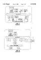
- the known PCI Local Bus system architecturehas also been adapted to a disk array controller 6 as shown in FIG. 2.
- the disk array controller 6includes a second DRAM connected to the PCI Local Bus through a RAID (Redundant Array of Independent Disks) Parity Assist (RPA) circuit.
- RAIDRedundant Array of Independent Disks
- the disk array controller 6also includes a System Input/Output (SIO) circuit which interfaces a bus such as an ISA (Industry Standard Architecture) bus to the PCI Local Bus, and one or more input/output processors (IOPs) which connect one or more disk drives 8 to the PCI Local Bus through a channel, such as a SCSI (Small Computer System Interface) bus.
- SIOSystem Input/Output
- IOPsinput/output processors
- the SIO circuitincludes arbitration logic which handles the PCI Local Bus arbitration.
- the disk drive 8includes one or more storage media (not shown) such as disks connected to each channel.
- a plurality of additional controller resourcessuch as non-volatile RAM, flash EPROM, Serial I/O port etc. are connected to the ISA bus.
- the SIO circuitincludes arbitration logic which handles the PCI Local Bus arbitration.
- the first or main memory DRAM of the disk array controller 6is typically implemented as a microprocessor code and data RAM for use in storing code and data for the processor.
- the second DRAMis typically implemented as a data transfer buffer for temporarily storing data to be read from or written to the one or more storage media across the PCI Local Bus.
- One disadvantage of the known PCI-based disk array controller architecture shown in FIG. 2is the cost of providing two separate DRAM subsystems within the disk array controller. Thus, the known PCI-based dual memory controller architecture is not suitable for low cost disk array controller applications.
- An additional disadvantage of the known PCI-based disk array controller architecture shown in FIG. 2is that a portion of the bandwidth of the PCI Local Bus is consumed by non-disk array-related data transfers across the PCI Local Bus such as data transfers between the processor and the resources connected to the ISA bus. More specifically, the processor must first arbitrate for the PCI Local Bus, and once access to the PCI Local Bus is granted, data is transferred across the PCI Local Bus thereby reducing the capacity of the PCI Local Bus to transfer data to/from the disk array.
- a method for transferring data in a controllerhaving a processor, a first bus and a controller resource, with the controller being connected between a host device and a disk drive.
- the methodincludes the steps of transferring first data between the host device and the disk drive across the first bus, and transferring second data between the processor and the controller resource without consuming any portion of the bandwidth of the first bus.
- a method for transferring data in a controller having a processor and a controller support device, with the controller connected to a host device and a disk driveincludes the steps of providing the controller with a first bus and a second bus, connecting a first bus between the disk drive and the host device, connecting a second bus between the processor and the controller support device, transferring first data between the disk drive and the host device across the first bus, and transferring second data between the processor and the controller support device across the second bus without consuming any portion of the bandwidth of the first bus.
- a controllerconnected to a host device and a disk drive, with the controller including a first bus connected between the host device and the disk drive, a processor, a controller support device, and a second bus connected between the processor and the controller support device, wherein all data transfers between the processor and the controller support device occur without consuming any portion of the bandwidth of the first bus.
- FIG. 1is a block diagram of a prior art PCI Local Bus system architecture implemented in a personal computer environment
- FIG. 2is a block diagram of a prior art PCI Local Bus system architecture implemented in a disk array controller environment
- FIG. 3is a block diagram of a first embodiment of a PCI-based disk array controller
- FIG. 4is a block diagram of a second embodiment of a PCI-based disk array controller
- FIG. 5is a block diagram of a second interface circuit of the disk array controllers shown in FIG. 3;
- FIG. 6is a block diagram of a third interface circuit of the disk array controller shown in FIGS. 3 and 4.
- the disk array controller 10includes a main processor 12 such as a microprocessor, a first interface circuit 14, a second interface circuit 16, a third interface circuit 18, a RAID Parity Assist (RPA) circuit 20, a RAM device 22 such as a DRAM, and one or more input/output processors (IOPs) 24.
- the main processor 12is a microprocessor from the Intel 80486 family of microprocessors.
- An exemplary microprocessoris the 80486SX-33 that is available from Intel Corporation.
- the processor 12includes an internal local bus 26 and one or more external input/output pins or pads which provide external access to the internal local bus 26.
- the first interface circuit 14 and the third interface circuit 18are connected to the internal local bus 26.
- the second interface circuit 16, third interface circuit 18, RPA circuit 20 and input/output processor 24are connected to a PCI Local Bus 28.
- the second interface circuit 16is also connected to a host PCI Local Bus 30 through a slot (not shown) such as a PCI Local Bus slot of a host device 31 such as a computer or a file server.
- the PCI Local Bus standardis defined in the document entitled PCI Local Bus Specification, Revision 2.1 which is available from the PCI Special Interest Group, P.O. Box 14070, Portland, Oreg. 97214, and which is incorporated herein by reference.
- the input/output processor 24is connected to one or more disk drives 33 through a channel 32, such as a SCSI bus.
- SCSIis a communications protocol standard for input/output devices.
- the first version of the standard, SCSI-1is described in ANSI Document No. X3.131-1986 which is incorporated herein by reference.
- the SCSI-1 specificationhas been upgraded with an expanded interface referred to as SCSI-2.
- the SCSI-2 specificationis described in ANSI Document No. X3.131-1994 which is also incorporated herein by reference.
- RAIDRedundant Array of Inexpensive Disks
- the input/output processor 24executes ASIC-specific (Application Specific Integrated Circuit) instructions independent from controller firmware which is executed by the processor 12.
- ASIC-specificApplication Specific Integrated Circuit
- An example of a suitable input/output processoris a SCSI Input/Output Processor (SIOP) 53C825A chip or 53C875 chip manufactured by Symbios Logic Inc. of Fort Collins, Colo.
- SIOPSCSI Input/Output Processor
- the 53C825A and 53C875 input/output processorsexecute SCRIPTS instructions which are an ASIC-specific instruction set specifically designed for controlling the 53C8XX family of Symbios Logic Inc. products.
- the RPA circuit 20includes memory controller circuitry and exclusive-OR (XOR) parity circuitry.
- the RPA circuit 20functions as a PCI-based DRAM controller and the DRAM 22 functions as a cache buffer. More specifically, read data is initially sent from one or more disk drives 33 connected to the channel 32 through the input/output processor 24 and across the PCI Local Bus 28 to the DRAM 22. Once the read data is stored in the DRAM 22, the processor 12 schedules a second operation where the read data is sent from the DRAM 22 back across the PCI Local Bus 28 and through the second interface circuit 16 to the host device 31.
- XORexclusive-OR
- "new" write datais initially sent from the host device 31 through the second interface circuit 16 and across the PCI Local Bus 28 to a first location within the DRAM 22.
- the "old” datais then read from a data disk of the disk drive 33 across the PCI Local Bus 28 into a second location within the DRAM 22, and the "old” parity information is read from a parity disk of the disk drive 33 across the PCI Local Bus 28 into a third location within the DRAM 22.
- the RPA circuit 20then independently and transparently performs conventional read-modify-write operations where "new" parity information is generated by exclusive-ORing the "old" data, "old” parity information and "new” data which are stored within the DRAM 22.
- the processor 12schedules a write operation to write the "new" write data to a data disk of the disk drive 33 from the DRAM 22 and/or "new" parity information to a parity disk of the disk drive 33 from the DRAM 22.
- a suitable RPA circuit 20is the RAID Parity Assist chip provided by Symbios Logic Inc. as part of their existing controller products.
- the first interface circuit 14includes circuitry for interfacing the processor 12 to one or more controller resources or devices 37 such as a battery-backed RAM and a flash EPROM which are connected to an auxiliary bus 38 such as, or similar to an ISA bus.
- controller resources or devices 37such as a battery-backed RAM and a flash EPROM which are connected to an auxiliary bus 38 such as, or similar to an ISA bus.
- non-disk array-related data transfers to/from the processor 12are sent across the processor local bus 26 through the first interface chip 14. It should be appreciated that this is an advantage over prior art designs such as shown in FIG. 2 in that the prior art architecture requires that non-disk array-related data transfers are sent across the PCI Local Bus thus consuming any portion of its available bandwidth. In contrast, the architecture of the present invention does not require non-disk array-related activity to be sent across the PCI Local Bus 28, thus increasing the bandwidth available for disk array-related data transfers across the PCI Local Bus 28.
- the second interface circuit 16includes circuitry for interfacing the PCI Local Bus 28 to the host PCI Local Bus 30. As shown in FIG. 5, the second interface circuit 16 includes a first PCI interface circuit 40, a second PCI interface circuit 41 and a high-bandwidth DMA (Direct memory Access) interface circuit 42.
- DMADirect memory Access
- the first PCI interface 40implements a conventional SCRIPTS engine which minimizes software impact by permitting existing software drivers to operate with the PCI-based controller 10. More specifically, when the host device 31 initiates a disk read/write operation, the host device 31 can use existing SCSI device drivers as well as performance enhanced disk array drivers to communicate with the PCI-based controller 10.
- the host device 31desires to write 64-Kbytes of data that is stored in separate blocks throughout the host memory to the disk drive 33
- the host device 31provides a conventional scatter-gather list to the SCRIPTS engine of the first PCI interface 40.
- the scatter-gather listindicates where the blocks of write data are located in a host memory map.
- the SCRIPTS engine implemented in the first PCI interface 40uses the scatter-gather list to build linked DMA (Direct Memory Access) operations which fetch the blocks of write data from the host device.
- the second PCI interface 41implements a separate conventional SCRIPTS engine which builds a separate scatter-gather list to indicate where the blocks of write data are to be stored in the disk drive 33.
- the total length of write data transferrede.g.
- the SCRIPTS engines in the first and second PCI interfaces 40, 42operate independently to transfer the blocks of write data from one scatter-gather list to a separate scatter-gather list across the DMA interface 44.
- the DMA interfacedecouples or buffers the operating speeds between the first and second PCI interfaces 40, 41.
- the host device PCI Local Bus 30could be operating at 25 MHz while the disk array PCI Local Bus 28 is operating at 33 MHz.
- the third interface circuit 18serves as a PCI bus master relative to the devices on the PCI Local Bus 28, and serves as both a PCI bus master and a PCI bus slave relative to the processor 12.
- the third interface circuitincludes circuit 44 which implements a first state machine such as an Intel 80486 state machine, circuit 46 which implements a second state machine such as a PCI Local Bus state machine, 4-word data buffer 48, 4-word address buffer 50, second level cache control circuitry 52 and arbitration logic 54.
- the first and second state machines that are implement by circuits 44, 46cooperate to convert or translate processor 12 bus cycles or control signals to equivalent PCI Local Bus 28 cycles or control signals in a known manner.
- the first and second state machines that are implemented by the circuits 44, 46permit processor 12 burst mode code and data fetching across the PCI Local Bus 28 by converting or translating processor 12 burst mode fetch cycles to equivalent PCI Local Bus 28 cycles as would be known to one of ordinary skill in the art.
- the first state machine implemented by the circuit 44translates Intel 80486SX/DX/DX2 burst mode fetch cycles of the processor 12 into appropriate PCI Local Bus 28 cycles.
- the appropriate PCI Local Bus cyclesare defined in the above-identified document entitled PCI Local Bus Specification, Revision 2.1.
- the processor 12 burst mode fetch cyclesare defined in the Intel 80486XX data book which is incorporated herein by reference.
- the third interface circuit 18also includes circuitry for fetching the processor code and/or data from the DRAM 22 across the PCI Local Bus 28 in linear address order, and presenting the code/data to the processor 12 in the nonlinear address order required by the processor 12.
- the 4-word data and address buffers 48, 50are used for executing posted writes to a device connected to the PCI Local Bus 28.
- the write data from the processor 12is latched into the data buffer 48 until the PCI Local Bus 28 is available for transferring the write data to the device designated in the address buffer 50.
- posted write data from the processor 12will be transferred out of the address buffer 50 across the PCI Local Bus 28 in a burst if the processor 12 executes a number of posted write operations to consecutive memory addresses of the DRAM 22.
- the second level cache control circuit 52supports an optional look-aside secondary cache 56 (FIG. 3) through one or more control lines 58 (FIG. 3).
- a suitable look-aside second level cacheis the CXK78486Q1-33 (cache-1C) integrated cache/controller chip, or the CX784862Q-33 (cache-2) integrated cache/controller chip, both of which are available from SONY Corporation.
- the SONY chipsare designed to work with the Intel 80486 family of processors by connecting directly to the processor local bus 26 as shown in phantom (FIG. 3), and caching data in a look-aside manner with minimal connection to the third interface circuit 18.
- the cache control circuits necessary to support secondary cache 56are internal to the secondary cache 56 rather than being included in the third interface chip 18 as provided in the known Intel 82424ZX CDC chip.
- the third interface circuit 18includes a support circuit which fetches code/data from the DRAM 22 or disk drive 33 in the event that the particular code/data requested by the processor 12 is not present in the first level cache internal to the processor 12 or the second level cache 56.
- the PCI arbitration logic 54handles all of the arbitration between the devices connected to the PCI Local Bus 28 through request lines 55a and grant lines 55b. If no devices are arbitrating for the PCI Local Bus 28, then by definition the third interface circuit 18 is granted access to the PCI Local Bus 28 for use in executing processor 12 bus cycles across the PCI Local Bus 28 such as fetching code from the DRAM 22 during a processor 12 burst code fetch operation. Many known arbitration schemes are suitable for implementation in the third interface circuit 18.
- the controller 60includes a second input/output processor (IOP) 62 connected to the PCI Local Bus 28 in place of the second interface chip 16 (FIG. 3).
- the second input/output processor 62is also connected through one or more cables 64, such as SCSI cables, to a third input/output processor (IOP) 66 associated with a SCSI host adapter 68 that is connected to a host SCSI Bus 70 through a slot (not shown) of a host device (not shown).
- datacan be transferred between the second and third input/output processors 62, 63 such as 53C825A SCSI Input/Output Processor chips, at a rate of approximately 20 MByte/sec, or 40 MByte/sec for a 53C875 chip.
- datacan be transferred between the first and second PCI interfaces 40, 41 (FIG. 5) at a rate of 132 Mb/sec which is the specified data transfer rate of the PCI Local Bus 28.
- the second input/output processor 62functions in the same manner as the second PCI interface 41 (FIG. 5), and the third input/output processor 66 functions in the same manner as the first PCI interface 40 (FIG. 5).
- datais transferred from one scatter-gather list to a separate scatter-gather list across a common SCSI-interface in the disk array controller 60 shown in FIG. 4.
- the second interface circuit 16(FIG. 3) transfers data from one scatter-gather list to a separate scatter-gather list across the high-bandwidth DMA interface 42 (FIG. 5) in the controller 10.
- the disk array controller architecture of the present inventionimproves the price/performance ratio of the controller 10 by permitting burst mode code/data fetching across the PCI Local Bus 28 through the third interface circuit 18, by providing code/data caching capability across the PCI Local Bus 28 through the third interface circuit 18, and by off-loading bandwidth to the auxiliary bus 38 across the internal local bus 26.
Landscapes
- Engineering & Computer Science (AREA)
- Theoretical Computer Science (AREA)
- General Engineering & Computer Science (AREA)
- Physics & Mathematics (AREA)
- General Physics & Mathematics (AREA)
- Computer Hardware Design (AREA)
- Human Computer Interaction (AREA)
- Memory System Of A Hierarchy Structure (AREA)
- Bus Control (AREA)
Abstract
Description
Claims (17)
Priority Applications (4)
| Application Number | Priority Date | Filing Date | Title |
|---|---|---|---|
| US08/506,148US5729705A (en) | 1995-07-24 | 1995-07-24 | Method and apparatus for enhancing throughput of disk array data transfers in a controller |
| JP19305696AJP3187720B2 (en) | 1995-07-24 | 1996-07-23 | Method and apparatus for improving the throughput of disk array data transfer in a controller |
| EP96305397AEP0756235A1 (en) | 1995-07-24 | 1996-07-23 | Method and apparatus for enhancing throughput of disk array data transfers in a controller |
| KR1019960030027AKR100271118B1 (en) | 1995-07-24 | 1996-07-24 | METHOD AND APPARATUS FOR ENHANCING THROUGHPUT OF DISK ARRAY DATA TRANSFERS IN A CONTROLLER |
Applications Claiming Priority (1)
| Application Number | Priority Date | Filing Date | Title |
|---|---|---|---|
| US08/506,148US5729705A (en) | 1995-07-24 | 1995-07-24 | Method and apparatus for enhancing throughput of disk array data transfers in a controller |
Publications (1)
| Publication Number | Publication Date |
|---|---|
| US5729705Atrue US5729705A (en) | 1998-03-17 |
Family
ID=24013394
Family Applications (1)
| Application Number | Title | Priority Date | Filing Date |
|---|---|---|---|
| US08/506,148Expired - LifetimeUS5729705A (en) | 1995-07-24 | 1995-07-24 | Method and apparatus for enhancing throughput of disk array data transfers in a controller |
Country Status (4)
| Country | Link |
|---|---|
| US (1) | US5729705A (en) |
| EP (1) | EP0756235A1 (en) |
| JP (1) | JP3187720B2 (en) |
| KR (1) | KR100271118B1 (en) |
Cited By (13)
| Publication number | Priority date | Publication date | Assignee | Title |
|---|---|---|---|---|
| US5966534A (en)* | 1997-06-27 | 1999-10-12 | Cooke; Laurence H. | Method for compiling high level programming languages into an integrated processor with reconfigurable logic |
| US5968153A (en)* | 1996-06-21 | 1999-10-19 | Digital Equipment Corporation | Mechanism for high bandwidth DMA transfers in a PCI environment |
| US6098114A (en)* | 1997-11-14 | 2000-08-01 | 3Ware | Disk array system for processing and tracking the completion of I/O requests |
| US6134630A (en)* | 1997-11-14 | 2000-10-17 | 3Ware | High-performance bus architecture for disk array system |
| US6138176A (en)* | 1997-11-14 | 2000-10-24 | 3Ware | Disk array controller with automated processor which routes I/O data according to addresses and commands received from disk drive controllers |
| US6504854B1 (en)* | 1998-04-10 | 2003-01-07 | International Business Machines Corporation | Multiple frequency communications |
| KR100375816B1 (en)* | 2000-10-10 | 2003-03-15 | 조용범 | PCI bus controller having DMA interface and HPI of DSP |
| US6560573B1 (en)* | 1999-07-30 | 2003-05-06 | Emc Corporation | Storage controller with hardware emulation controller for emulation between control processor and transfer circuitry compatible to different processor |
| US20040010680A1 (en)* | 2002-07-12 | 2004-01-15 | Smith Gerald Edward | Method and apparatus for configuration of RAID controllers |
| US20040054838A1 (en)* | 1997-12-31 | 2004-03-18 | Hoese Geoffrey B. | Storage router and method for providing virtual local storage |
| US20040064600A1 (en)* | 2002-09-30 | 2004-04-01 | Lee Whay Sing | Composite DMA disk controller for efficient hardware-assisted data transfer operations |
| USRE42761E1 (en) | 1997-12-31 | 2011-09-27 | Crossroads Systems, Inc. | Storage router and method for providing virtual local storage |
| US8719490B2 (en) | 2010-12-30 | 2014-05-06 | Huawei Technologies Co., Ltd. | Storage array, storage system, and data access method |
Families Citing this family (11)
| Publication number | Priority date | Publication date | Assignee | Title |
|---|---|---|---|---|
| US5963962A (en)* | 1995-05-31 | 1999-10-05 | Network Appliance, Inc. | Write anywhere file-system layout |
| WO1994029795A1 (en) | 1993-06-04 | 1994-12-22 | Network Appliance Corporation | A method for providing parity in a raid sub-system using a non-volatile memory |
| US5881254A (en)* | 1996-06-28 | 1999-03-09 | Lsi Logic Corporation | Inter-bus bridge circuit with integrated memory port |
| US5937174A (en)* | 1996-06-28 | 1999-08-10 | Lsi Logic Corporation | Scalable hierarchial memory structure for high data bandwidth raid applications |
| US5950225A (en)* | 1997-02-28 | 1999-09-07 | Network Appliance, Inc. | Fly-by XOR for generating parity for data gleaned from a bus |
| US6516351B2 (en) | 1997-12-05 | 2003-02-04 | Network Appliance, Inc. | Enforcing uniform file-locking for diverse file-locking protocols |
| US6279011B1 (en) | 1998-06-19 | 2001-08-21 | Network Appliance, Inc. | Backup and restore for heterogeneous file server environment |
| US6119244A (en)* | 1998-08-25 | 2000-09-12 | Network Appliance, Inc. | Coordinating persistent status information with multiple file servers |
| US6343984B1 (en) | 1998-11-30 | 2002-02-05 | Network Appliance, Inc. | Laminar flow duct cooling system |
| KR20020032136A (en) | 2000-10-25 | 2002-05-03 | 박성훈 | Large capacity auxiliary storage device using memory |
| CN102063274B (en)* | 2010-12-30 | 2013-10-09 | 华为技术有限公司 | Storage array and storage system and data access method |
Citations (13)
| Publication number | Priority date | Publication date | Assignee | Title |
|---|---|---|---|---|
| US4965801A (en)* | 1987-09-28 | 1990-10-23 | Ncr Corporation | Architectural arrangement for a SCSI disk controller integrated circuit |
| EP0416331A2 (en)* | 1989-08-31 | 1991-03-13 | Yokogawa Electric Corporation | Line computer |
| EP0487901A2 (en)* | 1990-11-29 | 1992-06-03 | Hewlett-Packard Company | Disk controller using a video ram |
| US5253348A (en)* | 1990-12-28 | 1993-10-12 | Apple Computer, Inc. | Method of arbitration for buses operating at different speeds |
| US5257391A (en)* | 1991-08-16 | 1993-10-26 | Ncr Corporation | Disk controller having host interface and bus switches for selecting buffer and drive busses respectively based on configuration control signals |
| US5287476A (en)* | 1991-06-07 | 1994-02-15 | International Business Machines Corp. | Personal computer system with storage controller controlling data transfer |
| US5289418A (en)* | 1992-02-14 | 1994-02-22 | Extended Systems, Inc. | Memory apparatus with built-in parity generation |
| US5363492A (en)* | 1990-08-31 | 1994-11-08 | Ncr Corporation | Internal bus for work station interfacing means |
| EP0629956A2 (en)* | 1993-05-28 | 1994-12-21 | International Business Machines Corporation | Bus-to-bus bridge for optimising data transfers between a system bus and a peripheral bus |
| US5379384A (en)* | 1992-06-05 | 1995-01-03 | Intel Corporation | Configuration data loopback in a bus bridge circuit |
| US5392407A (en)* | 1992-12-24 | 1995-02-21 | Ncr Corporation | Multi-port processor with peripheral component interconnect port and rambus port |
| US5434976A (en)* | 1992-09-28 | 1995-07-18 | Standard Microsystems Corporation | Communications controller utilizing an external buffer memory with plural channels between a host and network interface operating independently for transferring packets between protocol layers |
| US5542053A (en)* | 1994-11-30 | 1996-07-30 | International Business Machines Corporation | Bridge interface between two buses of a computer system with a direct memory access controller programmed by a scatter/gather programmer |
- 1995
- 1995-07-24USUS08/506,148patent/US5729705A/ennot_activeExpired - Lifetime
- 1996
- 1996-07-23JPJP19305696Apatent/JP3187720B2/ennot_activeExpired - Fee Related
- 1996-07-23EPEP96305397Apatent/EP0756235A1/ennot_activeWithdrawn
- 1996-07-24KRKR1019960030027Apatent/KR100271118B1/ennot_activeExpired - Fee Related
Patent Citations (13)
| Publication number | Priority date | Publication date | Assignee | Title |
|---|---|---|---|---|
| US4965801A (en)* | 1987-09-28 | 1990-10-23 | Ncr Corporation | Architectural arrangement for a SCSI disk controller integrated circuit |
| EP0416331A2 (en)* | 1989-08-31 | 1991-03-13 | Yokogawa Electric Corporation | Line computer |
| US5363492A (en)* | 1990-08-31 | 1994-11-08 | Ncr Corporation | Internal bus for work station interfacing means |
| EP0487901A2 (en)* | 1990-11-29 | 1992-06-03 | Hewlett-Packard Company | Disk controller using a video ram |
| US5253348A (en)* | 1990-12-28 | 1993-10-12 | Apple Computer, Inc. | Method of arbitration for buses operating at different speeds |
| US5287476A (en)* | 1991-06-07 | 1994-02-15 | International Business Machines Corp. | Personal computer system with storage controller controlling data transfer |
| US5257391A (en)* | 1991-08-16 | 1993-10-26 | Ncr Corporation | Disk controller having host interface and bus switches for selecting buffer and drive busses respectively based on configuration control signals |
| US5289418A (en)* | 1992-02-14 | 1994-02-22 | Extended Systems, Inc. | Memory apparatus with built-in parity generation |
| US5379384A (en)* | 1992-06-05 | 1995-01-03 | Intel Corporation | Configuration data loopback in a bus bridge circuit |
| US5434976A (en)* | 1992-09-28 | 1995-07-18 | Standard Microsystems Corporation | Communications controller utilizing an external buffer memory with plural channels between a host and network interface operating independently for transferring packets between protocol layers |
| US5392407A (en)* | 1992-12-24 | 1995-02-21 | Ncr Corporation | Multi-port processor with peripheral component interconnect port and rambus port |
| EP0629956A2 (en)* | 1993-05-28 | 1994-12-21 | International Business Machines Corporation | Bus-to-bus bridge for optimising data transfers between a system bus and a peripheral bus |
| US5542053A (en)* | 1994-11-30 | 1996-07-30 | International Business Machines Corporation | Bridge interface between two buses of a computer system with a direct memory access controller programmed by a scatter/gather programmer |
Cited By (51)
| Publication number | Priority date | Publication date | Assignee | Title |
|---|---|---|---|---|
| US5968153A (en)* | 1996-06-21 | 1999-10-19 | Digital Equipment Corporation | Mechanism for high bandwidth DMA transfers in a PCI environment |
| US5966534A (en)* | 1997-06-27 | 1999-10-12 | Cooke; Laurence H. | Method for compiling high level programming languages into an integrated processor with reconfigurable logic |
| US6708325B2 (en) | 1997-06-27 | 2004-03-16 | Intel Corporation | Method for compiling high level programming languages into embedded microprocessor with multiple reconfigurable logic |
| US6549981B2 (en) | 1997-11-14 | 2003-04-15 | 3Ware, Inc. | Disk array system with controllers that automate host side of ATA interface |
| US6098114A (en)* | 1997-11-14 | 2000-08-01 | 3Ware | Disk array system for processing and tracking the completion of I/O requests |
| US6134630A (en)* | 1997-11-14 | 2000-10-17 | 3Ware | High-performance bus architecture for disk array system |
| US6138176A (en)* | 1997-11-14 | 2000-10-24 | 3Ware | Disk array controller with automated processor which routes I/O data according to addresses and commands received from disk drive controllers |
| US6301625B1 (en) | 1997-11-14 | 2001-10-09 | 3Ware, Inc. | System and method for processing and tracking the completion of I/O requests in a disk array system |
| US6421760B1 (en)* | 1997-11-14 | 2002-07-16 | 3Ware, Inc. | Disk array controller, and components thereof, for use with ATA disk drives |
| US20080046602A1 (en)* | 1997-12-31 | 2008-02-21 | Crossroads Systems, Inc. | Storage router and method for providing virtual local storage |
| US7689754B2 (en) | 1997-12-31 | 2010-03-30 | Crossroads Systems, Inc. | Storage router and method for providing virtual local storage |
| US9785583B2 (en) | 1997-12-31 | 2017-10-10 | Crossroads Systems, Inc. | Storage router and method for providing virtual local storage |
| US8402194B2 (en) | 1997-12-31 | 2013-03-19 | Crossroads Systems, Inc. | Storage router and method for providing virtual local storage |
| US20040054838A1 (en)* | 1997-12-31 | 2004-03-18 | Hoese Geoffrey B. | Storage router and method for providing virtual local storage |
| US8402193B2 (en) | 1997-12-31 | 2013-03-19 | Crossroads Systems, Inc. | Storage router and method for providing virtual local storage |
| US6738854B2 (en)* | 1997-12-31 | 2004-05-18 | Crossroads Systems, Inc. | Storage router and method for providing virtual local storage |
| US6763419B2 (en) | 1997-12-31 | 2004-07-13 | Crossroads Systems, Inc. | Storage router and method for providing virtual local storage |
| US6789152B2 (en)* | 1997-12-31 | 2004-09-07 | Crossroads Systems, Inc. | Storage router and method for providing virtual local storage |
| US8046515B2 (en) | 1997-12-31 | 2011-10-25 | Crossroads Systems, Inc. | Storage router and method for providing virtual local storage |
| US7051147B2 (en) | 1997-12-31 | 2006-05-23 | Crossroads Systems, Inc. | Storage router and method for providing virtual local storage |
| US20060143322A1 (en)* | 1997-12-31 | 2006-06-29 | Hoese Geoffrey B | Storage router and method for providing virtual local storage |
| US20060218322A1 (en)* | 1997-12-31 | 2006-09-28 | Hoese Geoffrey B | Storage router and method for providing virtual local storage |
| US8028117B2 (en) | 1997-12-31 | 2011-09-27 | Crossroads Systems, Inc. | Storage router and method for providing virtual local storage |
| US20070299995A1 (en)* | 1997-12-31 | 2007-12-27 | Crossroads Systems, Inc. | Storage Router and Method for Providing Virtual Local Storage |
| USRE42761E1 (en) | 1997-12-31 | 2011-09-27 | Crossroads Systems, Inc. | Storage router and method for providing virtual local storage |
| US20080046601A1 (en)* | 1997-12-31 | 2008-02-21 | Crossroads Systems, Inc. | Storage router and method for providing virtual local storage |
| US7340549B2 (en) | 1997-12-31 | 2008-03-04 | Crossroads Systems, Inc. | Storage router and method for providing virtual local storage |
| US20080065808A1 (en)* | 1997-12-31 | 2008-03-13 | Hoese Geoffrey B | Storage router and method for providing virtual local storage |
| US20080307444A1 (en)* | 1997-12-31 | 2008-12-11 | Crossroads Systems, Inc | Storage router and method for providing virtual local storage |
| US7552266B2 (en) | 1997-12-31 | 2009-06-23 | Crossroads Systems, Inc. | Storage router and method for providing virtual local storage |
| US8015339B2 (en) | 1997-12-31 | 2011-09-06 | Crossroads Systems, Inc. | Storage router and method for providing virtual local storage |
| US7694058B2 (en) | 1997-12-31 | 2010-04-06 | Crossroads Systems, Inc. | Storage router and method for providing virtual local storage |
| US20100121993A1 (en)* | 1997-12-31 | 2010-05-13 | Hoese Geoffrey B | Storage router and method for providing virtual local storage |
| US20110035527A1 (en)* | 1997-12-31 | 2011-02-10 | Hoese Geoffrey B | Storage Router and Method for Providing Virtual Local Storage |
| US20110035528A1 (en)* | 1997-12-31 | 2011-02-10 | Hoese Geoffrey B | Storage Router and Method for Providing Virtual Local Storage |
| US20110040949A1 (en)* | 1997-12-31 | 2011-02-17 | Hoese Geoffrey B | Storage Router and Method for Providing Virtual Local Storage |
| US7934041B2 (en) | 1997-12-31 | 2011-04-26 | Crossroads Systems, Inc. | Storage router and method for providing virtual local storage |
| US7934040B2 (en) | 1997-12-31 | 2011-04-26 | Crossroads Systems, Inc. | Storage router and method for providing virtual local storage |
| US7937517B2 (en) | 1997-12-31 | 2011-05-03 | Crossroads Systems, Inc. | Storage router and method for providing virtual local storage |
| US7984224B2 (en) | 1997-12-31 | 2011-07-19 | Crossroads Systems, Inc. | Storage router and method for providing virtual local storage |
| US7984221B2 (en) | 1997-12-31 | 2011-07-19 | Crossroads Systems, Inc. | Storage router and method for providing virtual local storage |
| US7987311B2 (en) | 1997-12-31 | 2011-07-26 | Crossroads Systems, Inc. | Storage router and method for providing virtual local storage |
| US6504854B1 (en)* | 1998-04-10 | 2003-01-07 | International Business Machines Corporation | Multiple frequency communications |
| US6560573B1 (en)* | 1999-07-30 | 2003-05-06 | Emc Corporation | Storage controller with hardware emulation controller for emulation between control processor and transfer circuitry compatible to different processor |
| KR100375816B1 (en)* | 2000-10-10 | 2003-03-15 | 조용범 | PCI bus controller having DMA interface and HPI of DSP |
| US7020770B2 (en)* | 2002-07-12 | 2006-03-28 | Lsi Logic Corporation | Method and apparatus for configuration of RAID controllers |
| US20040010680A1 (en)* | 2002-07-12 | 2004-01-15 | Smith Gerald Edward | Method and apparatus for configuration of RAID controllers |
| US7219169B2 (en)* | 2002-09-30 | 2007-05-15 | Sun Microsystems, Inc. | Composite DMA disk controller for efficient hardware-assisted data transfer operations |
| US20040064600A1 (en)* | 2002-09-30 | 2004-04-01 | Lee Whay Sing | Composite DMA disk controller for efficient hardware-assisted data transfer operations |
| US8719490B2 (en) | 2010-12-30 | 2014-05-06 | Huawei Technologies Co., Ltd. | Storage array, storage system, and data access method |
| US9098404B2 (en) | 2010-12-30 | 2015-08-04 | Huawei Technologies Co., Ltd. | Storage array, storage system, and data access method |
Also Published As
| Publication number | Publication date |
|---|---|
| JP3187720B2 (en) | 2001-07-11 |
| KR100271118B1 (en) | 2000-11-01 |
| EP0756235A1 (en) | 1997-01-29 |
| KR970007655A (en) | 1997-02-21 |
| JPH09114596A (en) | 1997-05-02 |
Similar Documents
| Publication | Publication Date | Title |
|---|---|---|
| US5729705A (en) | Method and apparatus for enhancing throughput of disk array data transfers in a controller | |
| US5734848A (en) | Method and appartus for transferring data in a controller having centralized memory | |
| US5682509A (en) | Bus interface to a RAID architecture | |
| US6526477B1 (en) | Host-memory based raid system, device, and method | |
| US5522065A (en) | Method for performing write operations in a parity fault tolerant disk array | |
| US6370611B1 (en) | Raid XOR operations to synchronous DRAM using a read buffer and pipelining of synchronous DRAM burst read data | |
| US5333305A (en) | Method for improving partial stripe write performance in disk array subsystems | |
| US5206943A (en) | Disk array controller with parity capabilities | |
| US6529989B1 (en) | Intelligent expansion ROM sharing bus subsystem | |
| US5917723A (en) | Method and apparatus for transferring data between two devices with reduced microprocessor overhead | |
| US6128711A (en) | Performance optimization and system bus duty cycle reduction by I/O bridge partial cache line writes | |
| US6012120A (en) | Method and apparatus for providing DMA transfers between devices coupled to different host bus bridges | |
| US5621902A (en) | Computer system having a bridge between two buses with a direct memory access controller and an alternative memory access controller | |
| US6636927B1 (en) | Bridge device for transferring data using master-specific prefetch sizes | |
| US20020087786A1 (en) | Method, system, and data structures for superimposing data records in a first data format to memory in a second data format | |
| US5937174A (en) | Scalable hierarchial memory structure for high data bandwidth raid applications | |
| US6286074B1 (en) | Method and system for reading prefetched data across a bridge system | |
| KR19990029295A (en) | Method and system for I / O control in multiprocessor system using simultaneous access of variable width bus | |
| KR19990029294A (en) | Method and System for Bus Arbitration in Multiprocessor Systems Using Concurrent Access to Variable Width Buses | |
| US5911053A (en) | Method and apparatus for changing data transfer widths in a computer system | |
| EP0493960A2 (en) | A computer system employing fast buffer copying | |
| US6370616B1 (en) | Memory interface controller for datum raid operations with a datum multiplier | |
| US7188303B2 (en) | Method, system, and program for generating parity data | |
| US5933613A (en) | Computer system and inter-bus control circuit | |
| WO1993013475A1 (en) | Method for performing disk array operations using a nonuniform stripe size mapping scheme |
Legal Events
| Date | Code | Title | Description |
|---|---|---|---|
| AS | Assignment | Owner name:SYMBIOS LOGIC INC., COLORADO Free format text:ASSIGNMENT OF ASSIGNORS INTEREST;ASSIGNOR:WEBER, BRET S.;REEL/FRAME:007590/0426 Effective date:19950721 | |
| STCF | Information on status: patent grant | Free format text:PATENTED CASE | |
| AS | Assignment | Owner name:SYMBIOS, INC ., COLORADO Free format text:CHANGE OF NAME;ASSIGNOR:SYMBIOS LOGIC INC.;REEL/FRAME:009089/0936 Effective date:19971210 | |
| AS | Assignment | Owner name:LSI LOGIC CORPORATION, CALIFORNIA Free format text:ASSIGNMENT OF ASSIGNORS INTEREST;ASSIGNOR:SYMBIOS, INC.;REEL/FRAME:009500/0554 Effective date:19980922 | |
| FPAY | Fee payment | Year of fee payment:4 | |
| FPAY | Fee payment | Year of fee payment:8 | |
| FEPP | Fee payment procedure | Free format text:PAYER NUMBER DE-ASSIGNED (ORIGINAL EVENT CODE: RMPN); ENTITY STATUS OF PATENT OWNER: LARGE ENTITY Free format text:PAYOR NUMBER ASSIGNED (ORIGINAL EVENT CODE: ASPN); ENTITY STATUS OF PATENT OWNER: LARGE ENTITY | |
| FPAY | Fee payment | Year of fee payment:12 | |
| AS | Assignment | Owner name:DEUTSCHE BANK AG NEW YORK BRANCH, AS COLLATERAL AG Free format text:PATENT SECURITY AGREEMENT;ASSIGNORS:LSI CORPORATION;AGERE SYSTEMS LLC;REEL/FRAME:032856/0031 Effective date:20140506 | |
| AS | Assignment | Owner name:LSI CORPORATION, CALIFORNIA Free format text:CHANGE OF NAME;ASSIGNOR:LSI LOGIC CORPORATION;REEL/FRAME:033102/0270 Effective date:20070406 | |
| AS | Assignment | Owner name:AVAGO TECHNOLOGIES GENERAL IP (SINGAPORE) PTE. LTD Free format text:ASSIGNMENT OF ASSIGNORS INTEREST;ASSIGNOR:LSI CORPORATION;REEL/FRAME:035390/0388 Effective date:20140814 | |
| AS | Assignment | Owner name:AGERE SYSTEMS LLC, PENNSYLVANIA Free format text:TERMINATION AND RELEASE OF SECURITY INTEREST IN PATENT RIGHTS (RELEASES RF 032856-0031);ASSIGNOR:DEUTSCHE BANK AG NEW YORK BRANCH, AS COLLATERAL AGENT;REEL/FRAME:037684/0039 Effective date:20160201 Owner name:LSI CORPORATION, CALIFORNIA Free format text:TERMINATION AND RELEASE OF SECURITY INTEREST IN PATENT RIGHTS (RELEASES RF 032856-0031);ASSIGNOR:DEUTSCHE BANK AG NEW YORK BRANCH, AS COLLATERAL AGENT;REEL/FRAME:037684/0039 Effective date:20160201 |