US5729410A - Magnetic tunnel junction device with longitudinal biasing - Google Patents
Magnetic tunnel junction device with longitudinal biasingDownload PDFInfo
- Publication number
- US5729410A US5729410AUS08/757,422US75742296AUS5729410AUS 5729410 AUS5729410 AUS 5729410AUS 75742296 AUS75742296 AUS 75742296AUS 5729410 AUS5729410 AUS 5729410A
- Authority
- US
- United States
- Prior art keywords
- layer
- ferromagnetic layer
- sensing
- fixed
- biasing
- Prior art date
- Legal status (The legal status is an assumption and is not a legal conclusion. Google has not performed a legal analysis and makes no representation as to the accuracy of the status listed.)
- Expired - Lifetime
Links
Images


Classifications
- G—PHYSICS
- G11—INFORMATION STORAGE
- G11B—INFORMATION STORAGE BASED ON RELATIVE MOVEMENT BETWEEN RECORD CARRIER AND TRANSDUCER
- G11B5/00—Recording by magnetisation or demagnetisation of a record carrier; Reproducing by magnetic means; Record carriers therefor
- G11B5/127—Structure or manufacture of heads, e.g. inductive
- B—PERFORMING OPERATIONS; TRANSPORTING
- B82—NANOTECHNOLOGY
- B82Y—SPECIFIC USES OR APPLICATIONS OF NANOSTRUCTURES; MEASUREMENT OR ANALYSIS OF NANOSTRUCTURES; MANUFACTURE OR TREATMENT OF NANOSTRUCTURES
- B82Y25/00—Nanomagnetism, e.g. magnetoimpedance, anisotropic magnetoresistance, giant magnetoresistance or tunneling magnetoresistance
- B—PERFORMING OPERATIONS; TRANSPORTING
- B82—NANOTECHNOLOGY
- B82Y—SPECIFIC USES OR APPLICATIONS OF NANOSTRUCTURES; MEASUREMENT OR ANALYSIS OF NANOSTRUCTURES; MANUFACTURE OR TREATMENT OF NANOSTRUCTURES
- B82Y10/00—Nanotechnology for information processing, storage or transmission, e.g. quantum computing or single electron logic
- G—PHYSICS
- G01—MEASURING; TESTING
- G01R—MEASURING ELECTRIC VARIABLES; MEASURING MAGNETIC VARIABLES
- G01R33/00—Arrangements or instruments for measuring magnetic variables
- G01R33/02—Measuring direction or magnitude of magnetic fields or magnetic flux
- G01R33/06—Measuring direction or magnitude of magnetic fields or magnetic flux using galvano-magnetic devices
- G01R33/09—Magnetoresistive devices
- G01R33/093—Magnetoresistive devices using multilayer structures, e.g. giant magnetoresistance sensors
- G—PHYSICS
- G01—MEASURING; TESTING
- G01R—MEASURING ELECTRIC VARIABLES; MEASURING MAGNETIC VARIABLES
- G01R33/00—Arrangements or instruments for measuring magnetic variables
- G01R33/02—Measuring direction or magnitude of magnetic fields or magnetic flux
- G01R33/06—Measuring direction or magnitude of magnetic fields or magnetic flux using galvano-magnetic devices
- G01R33/09—Magnetoresistive devices
- G01R33/098—Magnetoresistive devices comprising tunnel junctions, e.g. tunnel magnetoresistance sensors
- G—PHYSICS
- G11—INFORMATION STORAGE
- G11B—INFORMATION STORAGE BASED ON RELATIVE MOVEMENT BETWEEN RECORD CARRIER AND TRANSDUCER
- G11B5/00—Recording by magnetisation or demagnetisation of a record carrier; Reproducing by magnetic means; Record carriers therefor
- G11B5/127—Structure or manufacture of heads, e.g. inductive
- G11B5/33—Structure or manufacture of flux-sensitive heads, i.e. for reproduction only; Combination of such heads with means for recording or erasing only
- G11B5/39—Structure or manufacture of flux-sensitive heads, i.e. for reproduction only; Combination of such heads with means for recording or erasing only using magneto-resistive devices or effects
- G11B5/3903—Structure or manufacture of flux-sensitive heads, i.e. for reproduction only; Combination of such heads with means for recording or erasing only using magneto-resistive devices or effects using magnetic thin film layers or their effects, the films being part of integrated structures
- G11B5/3906—Details related to the use of magnetic thin film layers or to their effects
- G11B5/3909—Arrangements using a magnetic tunnel junction
- G—PHYSICS
- G11—INFORMATION STORAGE
- G11C—STATIC STORES
- G11C11/00—Digital stores characterised by the use of particular electric or magnetic storage elements; Storage elements therefor
- G11C11/02—Digital stores characterised by the use of particular electric or magnetic storage elements; Storage elements therefor using magnetic elements
- G11C11/16—Digital stores characterised by the use of particular electric or magnetic storage elements; Storage elements therefor using magnetic elements using elements in which the storage effect is based on magnetic spin effect
- G11C11/161—Digital stores characterised by the use of particular electric or magnetic storage elements; Storage elements therefor using magnetic elements using elements in which the storage effect is based on magnetic spin effect details concerning the memory cell structure, e.g. the layers of the ferromagnetic memory cell
- G—PHYSICS
- G11—INFORMATION STORAGE
- G11C—STATIC STORES
- G11C11/00—Digital stores characterised by the use of particular electric or magnetic storage elements; Storage elements therefor
- G11C11/02—Digital stores characterised by the use of particular electric or magnetic storage elements; Storage elements therefor using magnetic elements
- G11C11/16—Digital stores characterised by the use of particular electric or magnetic storage elements; Storage elements therefor using magnetic elements using elements in which the storage effect is based on magnetic spin effect
- G11C11/165—Auxiliary circuits
- G11C11/1659—Cell access
- G—PHYSICS
- G11—INFORMATION STORAGE
- G11C—STATIC STORES
- G11C11/00—Digital stores characterised by the use of particular electric or magnetic storage elements; Storage elements therefor
- G11C11/02—Digital stores characterised by the use of particular electric or magnetic storage elements; Storage elements therefor using magnetic elements
- G11C11/16—Digital stores characterised by the use of particular electric or magnetic storage elements; Storage elements therefor using magnetic elements using elements in which the storage effect is based on magnetic spin effect
- G11C11/165—Auxiliary circuits
- G11C11/1673—Reading or sensing circuits or methods
- G—PHYSICS
- G11—INFORMATION STORAGE
- G11C—STATIC STORES
- G11C11/00—Digital stores characterised by the use of particular electric or magnetic storage elements; Storage elements therefor
- G11C11/02—Digital stores characterised by the use of particular electric or magnetic storage elements; Storage elements therefor using magnetic elements
- G11C11/16—Digital stores characterised by the use of particular electric or magnetic storage elements; Storage elements therefor using magnetic elements using elements in which the storage effect is based on magnetic spin effect
- G11C11/165—Auxiliary circuits
- G11C11/1675—Writing or programming circuits or methods
- H—ELECTRICITY
- H10—SEMICONDUCTOR DEVICES; ELECTRIC SOLID-STATE DEVICES NOT OTHERWISE PROVIDED FOR
- H10N—ELECTRIC SOLID-STATE DEVICES NOT OTHERWISE PROVIDED FOR
- H10N50/00—Galvanomagnetic devices
- H10N50/10—Magnetoresistive devices
- G—PHYSICS
- G11—INFORMATION STORAGE
- G11B—INFORMATION STORAGE BASED ON RELATIVE MOVEMENT BETWEEN RECORD CARRIER AND TRANSDUCER
- G11B5/00—Recording by magnetisation or demagnetisation of a record carrier; Reproducing by magnetic means; Record carriers therefor
- G11B5/127—Structure or manufacture of heads, e.g. inductive
- G11B5/33—Structure or manufacture of flux-sensitive heads, i.e. for reproduction only; Combination of such heads with means for recording or erasing only
- G11B5/39—Structure or manufacture of flux-sensitive heads, i.e. for reproduction only; Combination of such heads with means for recording or erasing only using magneto-resistive devices or effects
- G11B2005/3996—Structure or manufacture of flux-sensitive heads, i.e. for reproduction only; Combination of such heads with means for recording or erasing only using magneto-resistive devices or effects large or giant magnetoresistive effects [GMR], e.g. as generated in spin-valve [SV] devices
- G—PHYSICS
- G11—INFORMATION STORAGE
- G11B—INFORMATION STORAGE BASED ON RELATIVE MOVEMENT BETWEEN RECORD CARRIER AND TRANSDUCER
- G11B5/00—Recording by magnetisation or demagnetisation of a record carrier; Reproducing by magnetic means; Record carriers therefor
- G11B5/127—Structure or manufacture of heads, e.g. inductive
- G11B5/33—Structure or manufacture of flux-sensitive heads, i.e. for reproduction only; Combination of such heads with means for recording or erasing only
- G11B5/39—Structure or manufacture of flux-sensitive heads, i.e. for reproduction only; Combination of such heads with means for recording or erasing only using magneto-resistive devices or effects
- G11B5/3903—Structure or manufacture of flux-sensitive heads, i.e. for reproduction only; Combination of such heads with means for recording or erasing only using magneto-resistive devices or effects using magnetic thin film layers or their effects, the films being part of integrated structures
- G11B5/3906—Details related to the use of magnetic thin film layers or to their effects
- G11B5/3929—Disposition of magnetic thin films not used for directly coupling magnetic flux from the track to the MR film or for shielding
- G11B5/3932—Magnetic biasing films
Definitions
- This inventionrelates in general to a magnetic tunnel junction (MTJ) device, and more particularly to an MTJ device for use as a magnetoresistive (MR) head for reading magnetically-recorded data.
- MTJmagnetic tunnel junction
- MRmagnetoresistive
- a magnetic tunnel junction (MTJ) deviceis comprised of two ferromagnetic layers separated by a thin insulating tunnel barrier layer and is based on the phenomenon of spin-polarized electron tunneling.
- One of the ferromagnetic layershas a higher saturation field in one direction of an applied magnetic field, typically due to its higher coercivity than the other ferromagnetic layer.
- the insulating tunnel barrier layeris thin enough that quantum mechanical tunneling occurs between the ferromagnetic layers.
- the tunneling phenomenonis electron-spin dependent, making the magnetic response of the MTJ a function of the relative orientations and spin polarizations of the two ferromagnetic layers.
- the state of the MTJ memory cellis determined by measuring the resistance of the MTJ when a sense current is passed perpendicularly through the MTJ from one ferromagnetic layer to the other.
- the probability of tunneling of charge carriers across the insulating tunnel barrier layerdepends on the relative alignment of the magnetic moments (magnetization directions) of the two ferromagnetic layers.
- the tunneling currentis spin polarized, which means that the electrical current passing from one of the ferromagnetic layers, for example, a layer whose magnetic moment is fixed or prevented from rotation, is predominantly composed of electrons of one spin type (spin up or spin down, depending on the orientation of the magnetic moment of the ferromagnetic layer).
- the degree of spin polarization of the tunneling currentis determined by the electronic band structure of the magnetic material comprising the ferromagnetic layer at the interface of the ferromagnetic layer with the tunnel barrier layer.
- the first ferromagnetic layerthus acts as a spin filter.
- the probability of tunneling of the charge carriersdepends on the availability of electronic states of the same spin polarization as the spin polarization of the electrical current in the second ferromagnetic layer. Usually, when the magnetic moment of the second ferromagnetic layer is parallel to the magnetic moment of the first ferromagnetic layer, there are more available electronic states than when the magnetic moment of the second ferromagnetic layer is aligned antiparallel to that of the first ferromagnetic layer.
- the tunneling probability of the charge carriersis highest when the magnetic moments of both layers are parallel, and is lowest when the magnetic moments are antiparallel.
- the tunneling probabilitytakes an intermediate value.
- the electrical resistance of the MTJ memory celldepends on both the spin polarization of the electrical current and the electronic states in both of the ferromagnetic layers.
- the two possible magnetization directions of the ferromagnetic layer whose magnetization direction is not fixeduniquely define two possible bit states (0 or 1) of the memory cell.
- a magnetoresistive (MR) sensordetects magnetic field signals through the resistance changes of a read element, fabricated of a magnetic material, as a function of the strength and direction of magnetic flux being sensed by the read element.
- the conventional MR sensorsuch as that used as a MR read head for reading data in magnetic recording disk drives, operates on the basis of the anisotropic magnetoresistive (AMR) effect of the bulk magnetic material, which is typically permalloy (Ni 81 Fe 19 ).
- a component of the read element resistancevaries as the square of the cosine of the angle between the magnetization direction in the read element and the direction of sense current through the read element.
- Recorded datacan be read from a magnetic medium, such as the disk in a disk drive, because the external magnetic field from the recorded magnetic medium (the signal field) causes a change in the direction of magnetization in the read element, which in turn causes a change in resistance of the read element and a corresponding change in the sensed current or voltage.
- the signal fieldcauses a change in the direction of magnetization in the read element, which in turn causes a change in resistance of the read element and a corresponding change in the sensed current or voltage.
- an MTJ devicethat has a stable and linear output and can thus function as an MTJ MR read head which provides a linear response to the magnetic fields from the recorded medium.
- the inventionis an MTJ device with one fixed ferromagnetic layer and one sensing ferromagnetic layer on opposite sides of the tunnel barrier layer, and with a hard biasing ferromagnetic layer that is electrically insulated from but yet magnetostatically coupled with the sensing ferromagnetic layer.
- the magnetic tunnel junction in the MTJ deviceis formed on an electrical lead on a substrate and is made up of a stack of layers.
- the layers in the stackare an antiferromagnetic layer, a fixed ferromagnetic layer exchange biased with the antiferromagnetic layer so that its magnetic moment cannot rotate in the presence of an applied magnetic field, an insulating tunnel barrier layer in contact with the fixed ferromagnetic layer, and a sensing ferromagnetic layer in contact with the tunnel barrier layer and whose magnetic moment is free to rotate in the presence of an applied magnetic field.
- the stackis generally rectangularly shaped with parallel side edges so that the layers have contiguous edges.
- a layer of hard biasing ferromagnetic materialis located near to but spaced from the side edges of the sensing ferromagnetic layer to longitudinally bias the magnetic moment of the sensing ferromagnetic layer in a preferred direction in the absence of an applied magnetic field.
- a layer of electrically insulating materialisolates the hard biasing material from the electrical lead and the sensing ferromagnetic layer so that sense current is not shunted to the hard biasing material but is allowed to flow perpendicularly through the layers in the magnetic tunnel junction stack.
- FIG. 1is a simplified block diagram of a conventional magnetic recording disk drive for use with the MTJ MR read head according to the present invention.
- FIG. 2is a top view of the disk drive of FIG. 1 with the cover removed.
- FIG. 3is a vertical cross-section of a conventional inductive write head/MR read head with the MR read head located between shields and adjacent to the inductive write head.
- FIGS. 4A-4Bshow a cross-section view and a top view, respectively, of an MTJ MR read head of the present invention.
- FIG. 5is a perspective view of the MTJ MR read head of FIGS. 4A-4B for illustrating the arrangement of the various layers of material, including the structure for providing longitudinal biasing of the sensing ferromagnetic layer.
- FIGS. 6A-6Nillustrate steps in the fabrication of the MTJ MR read head of the present invention.
- the MTJ device of the present inventionwill be described below as embodied as a MR sensor in a magnetic recording disk drive, the invention is also applicable to other MTJ applications, such as memory cells, and other magnetic recording systems, such as magnetic tape recording systems.
- FIG. 1there is illustrated in sectional view a schematic of a prior art disk drive of the type using a MR sensor.
- the disk drivecomprises a base 10 to which are secured a disk drive motor 12 and an actuator 14, and a cover 11.
- the base 10 and cover 11provide a substantially sealed housing for the disk drive.
- a magnetic recording disk 16is connected to drive motor 12 by means of hub 18 to which it is attached for rotation by the drive motor 12.
- a thin lubricant film 50is maintained on the surface of disk 16.
- a read/write head or transducer 25is formed on the trailing end of a carrier, such as an air-bearing slider 20.
- Transducer 25is a read/write head comprising an inductive write head portion and a MR read head portion, as will be described with respect to FIG. 3.
- the slider 20is connected to the actuator 14 by means of a rigid arm 22 and a suspension 24.
- the suspension 24provides a biasing force which urges the slider 20 onto the surface of the recording disk 16.
- the drive motor 12rotates the disk 16 at a constant speed
- the actuator 14, which is typically a linear or rotary voice coil motor (VCM)moves the slider 20 generally radially across the surface of the disk 16 so that the read/write head 25 may access different data tracks on disk 16.
- VCMlinear or rotary voice coil motor
- FIG. 2is a top view of the interior of the disk drive with the cover 11 removed, and illustrates in better detail the suspension 24 which provides a force to the slider 20 to urge it toward the disk 16.
- the suspensionmay be a conventional type of suspension, such as the well-known Watrous suspension, as described in IBM's U.S. Pat. No. 4,167,765. This type of suspension also provides a gimbaled attachment of the slider which allows the slider to pitch and roll as it rides on the air bearing.
- the data detected from disk 16 by the transducer 25is processed into a data readback signal by signal amplification and processing circuitry in the integrated circuit chip 15 located on arm 22.
- the signals from transducer 25travel via flex cable 17 to chip 15, which sends its output signals to the disk drive electronics (not shown) via cable 19.
- FIG. 3is a cross-sectional schematic view of the read/write head 25 which includes a MR read head portion and an inductive write head portion.
- the head 25is lapped to form an air-bearing surface (ABS), the ABS being spaced from the surface of the rotating disk 16 (FIG. 1) by the air bearing as discussed above.
- the read headincludes a MR sensor 40 sandwiched between first and second gap layers G1 and G2 which are, in turn, sandwiched between first and second shield layers S1 and S2.
- the MR sensor 40is an AMR sensor.
- the write headincludes a coil layer C and insulation layer I2 which are sandwiched between insulation layers I1 and I3 which are, in turn, sandwiched between first and second pole pieces P1 and P2.
- a gap layer G3is sandwiched between the first and second pole pieces P1, P2 at their pole tips adjacent to the ABS for providing a magnetic gap.
- signal currentis conducted through the coil layer C and flux is induced into the first and second pole layers P1, P2 causing flux to fringe across the pole tips at the ABS.
- This fluxmagnetizes circular tracks on the rotating disk 16 during a write operation.
- magnetized regions on the rotating disk 16inject flux into the MR sensor 40 of the read head, causing resistance changes in the MR sensor 40. These resistance changes are detected by detecting voltage changes across the MR sensor 40.
- the voltage changesare processed by the chip 15 (FIG. 2) and drive electronics and converted into user data.
- the combined head 25 shown in FIG. 3is a "merged" head in which the second shield layer S2 of the read head is employed as a first pole piece P1 for the write head. In a piggyback head (not shown), the second shield layer S2 and the first pole piece P1 are separate layers.
- Disk drivesmay contain a large number of disks and actuators, and each actuator may support a number of sliders.
- the head carriermay be one which maintains the head in contact or near contact with the disk, such as in liquid bearing and other contact and near-contact recording disk drives.
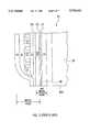
- the present inventionis a MR read head with an MTJ sensor for use in place of the MR sensor 40 in the read/write head 25 of FIG. 3.
- the MTJ MR read headincludes a bottom electrical lead 102 formed on the gap layer G1 substrate, a top electrical lead 104 below gap layer G2, and the MTJ 100 formed as a stack of layers between top and bottom electrical leads 102, 104.
- the MTJ 100includes a first electrode multilayer stack 110, an insulating tunnel barrier layer 120, and a top electrode stack 130.
- Each of the electrodesincludes a ferromagnetic layer in direct contact with tunnel barrier layer 120, i.e., ferromagnetic layers 118 and 132.
- the base electrode layer stack 110 formed on electrical lead 102includes a seed or "template” layer 112 on the lead 102, a layer of antiferromagnetic material 116 on the template layer 112, and a "fixed” ferromagnetic layer 118 formed on and exchange coupled with the underlying antiferromagnetic layer 116.
- the ferromagnetic layer 118is called the fixed layer because its magnetic moment or magnetization direction is prevented from rotation in the presence of applied magnetic fields in the desired range of interest.
- the top electrode stack 130includes a "sensing" ferromagnetic layer 132 and a protective or capping layer 134 formed on the sensing layer 132.
- the sensing ferromagnetic layer 132is not exchange coupled to an antiferromagnetic layer, and its magnetization direction is thus free to rotate in the presence of applied magnetic fields in the range of interest.
- the sensing ferromagnetic layer 132is fabricated so as to have its magnetic moment or magnetization direction (shown by arrow 133) oriented generally parallel to the ABS (FIG. 3) and generally perpendicular to the magnetization direction of the fixed ferromagnetic layer 118 in the absence of an applied magnetic field.
- the fixed ferromagnetic layer 118 in electrode stack 110 just beneath the tunnel barrier layer 120has its magnetization direction fixed by interfacial exchange coupling with the immediately underlying antiferromagnetic layer 116, which also forms part of bottom electrode stack 110.
- the magnetization direction of the fixed ferromagnetic layer 118is oriented generally perpendicular to the ABS, i.e., out of or into the paper in FIG. 4A (as shown by arrow tail 119).
- biasing ferromagnetic layer 150for longitudinally biasing the magnetization of the sensing ferromagnetic layer 132, and an insulating layer 160 separating and isolating the biasing layer 150 from the sensing ferromagnetic layer 132 and the other layers of the MTJ 100.
- the biasing ferromagnetic layer 150is a hard magnetic material, such as a CoPtCr alloy, that has its magnetic moment (shown by arrow 151) aligned in the same direction as the magnetic moment 133 of the sensing ferromagnetic layer 132 in the absence of an applied magnetic field.
- the insulating layer 160which is preferably alumina (A1 2 O 3 ) or silica (SiO 2 ), has a thickness sufficient to electrically isolate the biasing layer 150 from the MTJ 100 and the electrical leads 102, 104, but is still thin enough to permit magnetostatic coupling (shown by dashed arrow 153) with the sensing ferromagnetic layer 132.
- the product M*t (where M is the magnetic moment per unit area of the material in the ferromagnetic layer and t is the thickness of the ferromagnetic layer) of the biasing ferromagnetic layer 150must be greater than or equal to the M*t of the sensing ferromagnetic layer 132 to assure stable longitudinal biasing.
- the thickness of the biasing ferromagnetic layer 150should be at least approximately twice that of the sensing ferromagnetic layer 132.
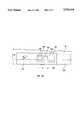
- FIG. 4Bis a top view of the MTJ MR head of FIG. 4A with the layers above and including the G2 layer removed and the top electrical lead 104 shown in dotted lines so that the underlying head can be illustrated.
- the dashed line 161represents the ABS and the line to which the layers are lapped back after the MTJ MR head is fabricated.
- the MTJ 100is depicted as a stripe having a width TW, appropriate to the track width of the recorded data on the disk, and a final stripe height SH after lapping. The width of the recorded data track is wider than TW.
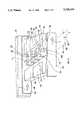
- FIG. 5is a schematic perspective view of the MTJ MR read head of FIGS. 4A-4B shown adjacent to a magnetic recording medium, such as the disk of a disk drive, and depicts the important layers of the MTJ 100 separated for ease in illustrating the operation of the read head.
- a data track 180 having a track width TW on the diskis shown with recorded data that generates a magnetic field h in the direction indicated by arrow 182.
- the fixed ferromagnetic layer 118has its magnetic moment, indicated by arrow 184, oriented perpendicular to the ABS and generally parallel or antiparallel to the magnetic field direction h from the disk.
- the direction 184is fixed, even in the presence of applied magnetic field h from recorded data, due to interfacial exchange coupling from adjacent antiferromagnetic layer 116.
- the sensing ferromagnetic layer 132has a generally rectangular shape with a sensing edge (not shown) at the ABS, a back edge 192, and two parallel side edges 194, 196. As shown, the other layers of MTJ 100 have edges generally contiguous with the edges of layer 132.
- the ferromagnetic sensing layer 132has its magnetic moment aligned in the direction parallel to the ABS and the disk surface, as indicated by arrow 133, in the absence of an applied magnetic field.
- the biasing ferromagnetic layer 150has its magnetic moment, indicated by arrow 151, aligned generally parallel with direction 133 to provide the sensing ferromagnetic layer 132 with a generally single magnetic domain state. Magnetostatic coupling occurs across the insulating layer 160 that electrically isolates the hard magnetic material of biasing layer 150 from the MTJ 100.
- a sense current Iis directed from first electrical lead 102 perpendicularly through the antiferromagnetic layer 116, the fixed ferromagnetic layer 118, the tunnel barrier layer 120, and the sensing ferromagnetic layer 132 and then out through the second electrical lead 104.
- the amount of tunneling current through the tunnel barrier layer 120is a function of the relative orientations of the magnetizations of the fixed and sensing ferromagnetic layers 118, 132 that are adjacent to and in contact with the tunnel barrier layer 120.
- the magnetic field h from the recorded datacauses the magnetization direction of sensing ferromagnetic layer 132 to rotate away from the direction 133, as shown by the dashed arrows 187, 189.
- This change in resistanceis detected by the disk drive electronics and processed into data read back from the disk.
- the sense currentis prevented from reaching the biasing ferromagnetic layer 150 by the electrical insulating layer 160, which also insulates the biasing ferromagnetic layer 150 from the electrical leads 102, 104. While in the preferred embodiment the biasing ferromagnetic layer 150 is electrically insulated from both leads 102, 104, it could be formed in contact with one of the leads so long as it is insulated from the other lead and the tunnel barrier layer 120.
- the insulating layer 160thus assures that there is no shunting of sense current and thus no adverse affect on the resistance of the MTJ MR head, while at the same time permitting magnetostatic coupling into the sensing ferromagnetic layer 132 by the biasing ferromagnetic layer 150.
- the insulating layer 160 and the ferromagnetic layer 150are formed using three distinct depositions.
- a first alumina depositionforms the bottom portion of layer 160 and also conforms onto the side edges 194 and 196 of the sensing ferromagnetic layer 132 (FIG. 4A). If an RF sputter deposition technique is used for the insulating layer deposition, the thickness of the insulating layer on the side wall is less than on a fiat surface. Typical sputter efficiencies on side walls are 1/2 to 3/4 that of the sputter efficiencies on fiat surfaces.
- the hard biasing ferromagnetic layer 150is deposited using a directional deposition technique, such as ion beam deposition.
- alumina from the first insulating layer deposition that conforms to the side walls 194, 196serves to insulate the biasing ferromagnetic layer 150 from the sensing ferromagnetic layer 132.
- a final insulating layer depositionforms the top region of layer 160 and caps or seals the top surface of the biasing ferromagnetic layer 150.
- the thickness of the first insulating layer depositionmust be sufficient to electrically isolate the biasing ferromagnetic layer 150 from both the bottom lead 102 and side walls 194, 196. Such insulation can be achieved with minimum alumina thickness of 100 ⁇ or a range of 100-500 ⁇ .
- the thickness of the second insulating layer depositionmust be sufficient to electrically isolate the biasing ferromagnetic layer 150 from the top lead 104. Such insulation can be achieved with alumina thickness in the range of 100-500 ⁇ .
- the thicknesses of the first and second insulating layer depositions that form insulating layer 160are limited by several factors. First, in order for the top lead structure 104 to conform over layer 160 and onto the MTJ 100 structure, the sum of the thickness of the first and second depositions must be close to the total thickness of the MTJ 100 structure, i.e., no more than 2 ⁇ greater and ideally closer to 1 ⁇ . Second, in order for the magnetostatic coupling field from the biasing ferromagnetic layer 150 to efficiently interact with the sensing ferromagnetic layer 132, the thickness of the first alumina deposition forming layer 160 must be sufficiently less than the thickness of the first and second gaps (G1 and G2).
- insulating layer 160which is formed by two separate alumina depositions, serves to electrically isolate the biasing ferromagnetic layer 150 from the sensing ferromagnetic layer 132 of the MTJ 100 structure.
- the degree of ferromagnetic coupling between these two layersis determined by the thickness of the two depositions and is best when the thickness is minimized relative to the thickness of the first and second gaps, but not to the extreme of compromising the insulating integrity between the free layer and the ferromagnetic bias layer.
- a representative set of materials for MTJ 100(FIG. 4A) will now be described. All of the layers of the MTJ 100 are grown in the presence of a magnetic field applied parallel to the surface of the substrate. The magnetic field serves to orient the easy axis of all of the ferromagnetic layers.
- a 5 nm Ta seed layer(not shown) is first formed on a 10-50 nm Au layer that serves as the bottom electrical lead 102.
- the seed layeris comprised of a material which encourages the (111) growth of the face-centered cubic (fcc) Ni 81 Fe 19 template layer 112.
- the template ferromagnetic layer 112encourages the growth of the antiferromagnetic layer 116.
- Suitable seed layer materialsinclude fcc metals, such as Cu, as well as Ta or a combination of layers, such as 3-5 nm Ta/3-5 nm Cu.
- the MTJ base electrode stack 110comprises a stack of 4 nm Ni 81 Fe 19 /10 nm Mn 50 Fe 50 /8 nm Ni 81 Fe 19 (layers 112, 116, 118, respectively) grown on the Ta seed layer on the 10-20 nm Au layer 102.
- the Au layer 102is formed on the alumina gap material G1 that serves as the substrate.
- the tunnel barrier layer 120is formed by depositing and then plasma oxidizing a 0.8-2 m Al layer. This creates the Al 2 O 3 insulating tunnel barrier layer 120.
- the top electrode stack 130is a 5 nm Ni-Fe/10 nm Ta stack (layers 132, 134, respectively).
- the Ta layer 134serves as a protective capping layer.
- the top electrode stack 130is contacted by a 20 nm Au layer that serves as the top electrical lead 104.
- the resistance of the MTJ devicewill be largely dominated by that of the tunnel barrier layer 120.
- the resistance per unit area of the conducting leads 102, 104can be much higher than in conventional MR read heads in which the current flows parallel to the layers.
- the leads 102, 104can be made thinner and/or narrower than in conventional MR head structures, and/or can be made from intrinsically more resistive materials, such as alloys or combinations of elements.
- the layers in the bottom electrode stack 110be smooth, and that the Al 2 O 3 tunnel barrier layer 120 be free of pinholes which would electrically short the junction.
- growth by sputtering techniques known to produce good giant magnetoresistance effects in metallic multilayer stacksis sufficient.
- the direction of the magnetic moments of the fixed and sensing ferromagnetic layers 118, 132, respectivelyare approximately orthogonal to one another in zero applied magnetic field.
- the direction of the moment of the fixed layer 118is largely determined by that of the exchange anisotropy field of the antiferromagnetic layer 116.
- the orientation of the moment of the sensing layer 132is influenced by a member of factors, including the intrinsic anisotropy of the ferromagnetic layer itself and the shape of this layer.
- An intrinsic magnetic anisotropycan be induced in the sensing layer 132 by depositing it in a small magnetic field arranged to be perpendicular to that of the magnetization direction of the fixed layer 118. If the shape of the sensing layer 132 is not square, there may be a magnetic anisotropy resulting from the rectangular shape of the sensing layer.
- TWlength of the sensing layer
- the intrinsic and shape anisotropiescan be arranged to favor the proper orientation of the magnetic moment of the sensing layer perpendicular to that of the fixed layer.
- neither of these anisotropiesis essential for the proper operation of the MTJ MR head.
- Proper orientation of the moment of sensing layer 132can be accomplished by the presence of the biasing ferromagnetic layer 150 alone.
- the magnetostriction of the sensing layer 132is arranged to be close to zero (by choice of composition of the Ni--Fe alloy) so that any stresses in this layer induced by the fabrication process do not, of themselves, lead to any magnetic anisotropy.
- An alternative sensing ferromagnetic layer 132may be comprised of a thin Co or Co.sub.(100-x) Fe.sub.(x) or Ni.sub.(100-x) Fe x (x is approximately 60) layer at the interface between the sensing ferromagnetic layer 132 and the tunnel barrier layer 120, with the bulk of layer 132 being a low magnetostriction material, such as Ni.sub.(100-x) Fe x (x is approximately 19).
- An alternative fixed ferromagnetic layer 118may be comprised largely of a bulk Ni.sub.(100-x) Fe.sub.(x) layer with a thin layer of a Co or Co.sub.(100-x) Fe.sub.(x) or Ni.sub.(100-x) Fe x (x is approximately 60) layer at the interface with the tunnel barrier layer 120.
- the largest signalis obtained with Co or with the highest polarization Ni.sub.(100-x) Fe x (x is approximately 60) or Co.sub.(100-x) Fe.sub.(x) alloy (x is approximately 70).
- the interface layeris optimally about 1-2 nm thick.
- the net magnetostriction of the combined layeris arranged to be dose to zero by small variations of the composition. If the bulk of layer 118 is Ni--Fe, then the composition is Ni 81 Fe 19 , the composition for which bulk Ni--Fe has zero magnetostriction.
- the Fe--Mn antiferromagnetic layer 116may be replaced with a Ni--Mn layer or other suitable antiferromagnetic layer which exchange biases the ferromagnetic material in the fixed layer 118 and which has a resistance which is substantially less than that of the Al 2 O 3 barrier layer.
- the stability of the fixed ferromagnetic layer 118can be increased further by forming it from a lamination of two magnetic layers, such as Ni, Co, Ni--Fe alloys, Co--Fe alloys, or Ni--Fe--Co ternary alloys, separated by a thin metallic layer, which results in antiferromagnetic coupling of the two magnetic layers.
- This type of laminated fixed layeris described in IBM's U.S. Pat. No. 5,465,185.
- FIGS. 6A-6NThe process for preparing the MTJ MR read head according to the present invention will be described with reference to the process flow diagram of FIGS. 6A-6N.
- the figures on the leftrepresent cross-sectional views of the individual layers as they are deposited and patterned, and the figures on the right represent the corresponding top view to illustrate lithographic patterning to ultimately create the MTJ MR read head as shown, for example, in FIG. 4B.
- the substrate (not shown) onto which the layers are depositedis the G1 alumina layer.
- Film growthsare carried out by magnetron sputtering with argon (Ar) gas with the substrate at ambient temperature. Care must be taken to ensure that the sputter growth produces very smooth films.
- An applied magnetic field of magnitude 20-100 Oe, with the field direction in the plane of the substrate (and in the direction from left to fight in the figures)may be used to induce magnetic anisotropy into the magnetic layers as they are grown.
- the aluminum layer which is to become the tunnel barrier layer 120is deposited and then subsequently plasma oxidized at an oxygen pressure of 100 mTorr and a power density of 25 W/cm 2 for 30-240 seconds. This forms the insulating tunnel barrier layer 120 of alumina.
- the plasma oxidation of the aluminum layeris done without breaking vacuum in the process.
- the substratePrior to the deposition of the sensing ferromagnetic layer 132 in the MTJ 100 and after formation of the alumina tunnel barrier layer 120, the substrate is rotated approximately 90 degrees in the plane of the substrate so as to be generally transverse to the applied magnetic field. Alternatively, the external applied magnetic field can be rotated.
- the MTJ device described and shown in FIG. 4Ahas the fixed ferromagnetic layer on the bottom of MTJ 100
- the devicecan also be formed by depositing the sensing ferromagnetic layer first, followed by the tunnel barrier layer, the fixed ferromagnetic layer, and the antiferromagnetic layer. Such an MTJ device would then have the layers essentially inverted from the MTJ 100 shown in FIG. 4A.
- FIG. 6AThe process starts in FIG. 6A with the sequential deposition of bottom lead 102 and MTJ 100 (which includes the top capping layer 134). These layers are then patterned into the shape of the bottom electrical lead 102, as shown by FIG. 6B.
- FIG. 6Clithography is used to define the track width TW of the MTJ 100.
- a positive photoresist 190has been applied to the lead 102 and MTJ 100 and developed to define the track width.
- islands of materialare removed from the MTJ 100 by ion milling down to the electrical lead layer 102.
- capping layer 134it may also be possible to reactively ion etch the capping layer 134 before ion milling the remaining MTJ layers.
- the deposition of the initial alumina insulator layer 160, CoPtCr hard biasing ferromagnetic layer 150, and subsequent alumina insulator layer 160are deposited through the openings in photoresist 190, leaving islands of electrically isolated longitudinal biasing material that forms the biasing ferromagnetic layer 150.
- the initial alumina layer 160 and subsequent alumina layer 160are preferably formed by RF sputtering to provide full coverage over electrical lead 102 and at the edges of MTJ 100 and are each formed to a thickness of 100-500 ⁇ . This process results in an insulator with high integrity since it is important that the sense current not be shunted through the hard biasing layer 150.
- the hard biasing layer 150which is preferably a CoPtCr alloy, is preferably formed directionally by a directional deposition process, such as ion beam sputter deposition, so there is no edge overlap, and is deposited to a thickness of approximately twice the thickness of the sensing layer 132.
- the photoresist 190 and the alumina and hard biasing layers on top of itare then removed, resulting in the electrically isolated regions of hard biasing ferromagnetic layer 150 that are located at the side edges of the magnetic tunnel junction that define the track width TW (FIGS. 6G-6H).
- lithographyis used to form the initial stripe height (before lapping) of the MTJ 100 by deposition and patterning of photoresist 191 (FIGS.
- the magnetization direction 133 of the ferromagnetic sensing layer 132must be maintained in the direction shown in FIG. 4A, i.e., along the longitudinal direction with no transverse components. This is accomplished by balancing the ferromagnetic coupling field H fc between the sensing and fixed ferromagnetic layers with the demagnetization field H d from the fixed ferromagnetic layer. Note that in an MTJ device, since the tunneling current is flowing normal to the layers of the structure, little field is induced from current flow in the films. H fc depends critically on the nature of the interfaces between the ferromagnetic films and the actual junction and the thickness of the junction.
- H fccan vary from several Oersteds (Oe) to 20-50 Oe.
- H ddepends on the geometry of the sensor, i.e., final stripe height SH and fixed ferromagnetic layer thickness t, and the fixed ferromagnetic magnetization M, and varies as (t/SH) ⁇ M!.
- SHfinal stripe height
- tfixed ferromagnetic layer thickness
- Mfixed ferromagnetic magnetization M
- H dis in the 40 Oe range.
- H dcan be matched to H fc .
- One manner of balancing these two forcesis to design a sensor that minimizes both fields.
- H dcan be minimized by using the laminated antiparallel fixed layer described in the previously-cited IBM U.S. Pat. No. 5,465,185.
- the net magnetic moment of such a layeris equivalent to the difference between the two pinned films, this difference being approximately 5 ⁇ , so that H d is reduced to approximately 4 Oe.
- the Fe--Mn layer 116 for exchange coupling with the fixed ferromagnetic layer 118is antiferromagnetic as deposited. However, its magnetization must be realigned so that it can exchange couple the fixed ferromagnetic layer 118 in the proper orientation.
- the structureis placed in an annealing oven and the temperature is raised to approximately 180° C., which is greater than the blocking temperature of Fe--Mn. At this temperature, the Fe--Mn layer no longer gives rise to an exchange anisotropy with the fixed ferromagnetic layer 118.
- An exchange anisotropy of the ferromagnetic layer 118is developed by cooling the pair of layers 116, 118 in a magnetic field.
- the orientation of the magnetization of the fixed ferromagnetic layer 118will be along the direction of the applied magnetic field.
- the applied magnetic field in the annealing oventhus causes the moment of the fixed ferromagnetic layer 118 to be fixed along the required direction perpendicular to the ABS, as shown by the arrow 184 in FIG. 5.
- Thisis a result of cooling the Fe--Mn layer in the presence of the ferromagnetic layer 118, magnetized by the applied magnetic field, in the required direction.
- the magnetization of the fixed ferromagnetic layer 118will not substantially rotate.
- the final stripe height SH of the MTJ 100 in the deviceis formed by lapping the lithographically-formed front sensing edge to a final dimension back to line 161, thereby completing the structure shown in FIGS. 4A-4B.
- the fixed ferromagnetic layerhas its preferred magnetization direction fixed, in the absence of an applied magnetic field, so as to be either parallel or antiparallel to the magnetization direction of the sensing ferromagnetic layer, which is longitudinally biased by the electrically isolated ferromagnetic biasing layer.
- the magnetization direction of the sensing ferromagnetic layeris rotated 180 degrees.
- the sense circuitrydetermines whether the memory cell is a "one" or a "zero” by detecting the electrical resistance, which depends on whether the ferromagnetic layers are aligned parallel or antiparallel.
Landscapes
- Engineering & Computer Science (AREA)
- Physics & Mathematics (AREA)
- Nanotechnology (AREA)
- Chemical & Material Sciences (AREA)
- Computer Hardware Design (AREA)
- Manufacturing & Machinery (AREA)
- Condensed Matter Physics & Semiconductors (AREA)
- Crystallography & Structural Chemistry (AREA)
- General Physics & Mathematics (AREA)
- Theoretical Computer Science (AREA)
- Mathematical Physics (AREA)
- Magnetic Heads (AREA)
- Hall/Mr Elements (AREA)
Abstract
Description
Claims (14)
Priority Applications (4)
| Application Number | Priority Date | Filing Date | Title |
|---|---|---|---|
| US08/757,422US5729410A (en) | 1996-11-27 | 1996-11-27 | Magnetic tunnel junction device with longitudinal biasing |
| KR1019970033906AKR100259428B1 (en) | 1996-11-27 | 1997-07-19 | Magnetic tunnel junction device with longitudinal biasing |
| JP27770597AJP3177199B2 (en) | 1996-11-27 | 1997-10-09 | Magnetic tunnel junction device and magnetoresistive read head |
| SG1997003873ASG60136A1 (en) | 1996-11-27 | 1997-10-27 | Magnetic tunnel junction device with longitudinal biasing |
Applications Claiming Priority (1)
| Application Number | Priority Date | Filing Date | Title |
|---|---|---|---|
| US08/757,422US5729410A (en) | 1996-11-27 | 1996-11-27 | Magnetic tunnel junction device with longitudinal biasing |
Publications (1)
| Publication Number | Publication Date |
|---|---|
| US5729410Atrue US5729410A (en) | 1998-03-17 |
Family
ID=25047759
Family Applications (1)
| Application Number | Title | Priority Date | Filing Date |
|---|---|---|---|
| US08/757,422Expired - LifetimeUS5729410A (en) | 1996-11-27 | 1996-11-27 | Magnetic tunnel junction device with longitudinal biasing |
Country Status (4)
| Country | Link |
|---|---|
| US (1) | US5729410A (en) |
| JP (1) | JP3177199B2 (en) |
| KR (1) | KR100259428B1 (en) |
| SG (1) | SG60136A1 (en) |
Cited By (162)
| Publication number | Priority date | Publication date | Assignee | Title |
|---|---|---|---|---|
| US5862022A (en)* | 1996-09-19 | 1999-01-19 | Tdk Corporation | Ferromagnetic tunnel junction, magnetoresistive element and magnetic head |
| US5898547A (en)* | 1997-10-24 | 1999-04-27 | International Business Machines Corporation | Magnetic tunnel junction magnetoresistive read head with sensing layer as flux guide |
| US5898548A (en)* | 1997-10-24 | 1999-04-27 | International Business Machines Corporation | Shielded magnetic tunnel junction magnetoresistive read head |
| US5901018A (en)* | 1997-10-24 | 1999-05-04 | International Business Machines Corporation | Magnetic tunnel junction magnetoresistive read head with sensing layer as rear flux guide |
| US5912790A (en)* | 1996-03-15 | 1999-06-15 | Kabushiki Kaisha Toshiba | Thin film magnetic recording-reproducing head having a high recording density and high fidelity |
| US5936293A (en)* | 1998-01-23 | 1999-08-10 | International Business Machines Corporation | Hard/soft magnetic tunnel junction device with stable hard ferromagnetic layer |
| US5953248A (en)* | 1998-07-20 | 1999-09-14 | Motorola, Inc. | Low switching field magnetic tunneling junction for high density arrays |
| US5973889A (en)* | 1997-02-20 | 1999-10-26 | U.S. Philips Corporation | Single-channel magnetic head with magnetoresistive element in series with electrically conducting magnetic elements |
| US6005753A (en)* | 1998-05-29 | 1999-12-21 | International Business Machines Corporation | Magnetic tunnel junction magnetoresistive read head with longitudinal and transverse bias |
| WO2000004592A1 (en)* | 1998-07-20 | 2000-01-27 | Motorola, Inc. | Fabricating an mtj with low areal resistance |
| US6023395A (en)* | 1998-05-29 | 2000-02-08 | International Business Machines Corporation | Magnetic tunnel junction magnetoresistive sensor with in-stack biasing |
| WO2000011664A1 (en)* | 1998-08-25 | 2000-03-02 | Koninklijke Philips Electronics N.V. | Thin film shielded magnetic read head device |
| EP0953849A3 (en)* | 1998-04-30 | 2000-03-15 | Hitachi, Ltd. | Spin tunnel magneto-resistance effect type magnetic sensor and production method thereof |
| WO2000022612A1 (en)* | 1998-10-12 | 2000-04-20 | Fujitsu Limited | Magnetic sensor, magnetic head, magnetic encoder, and hard disk drive |
| US6064552A (en)* | 1997-03-18 | 2000-05-16 | Kabushiki Kaisha Toshiba | Magnetoresistive head having magnetic yoke and giant magnetoresistive element such that a first electrode is formed on the giant magnetoresistive element which in turn is formed on the magnetic yoke which acts as a second electrode |
| US6084752A (en)* | 1996-02-22 | 2000-07-04 | Matsushita Electric Industrial Co., Ltd. | Thin film magnetic head |
| US6097579A (en)* | 1998-08-21 | 2000-08-01 | International Business Machines Corporation | Tunnel junction head structure without current shunting |
| US6115224A (en)* | 1997-10-24 | 2000-09-05 | Alps Electric Co., Ltd. | Spin-valve type thin film element and its manufacturing method |
| US6114719A (en)* | 1998-05-29 | 2000-09-05 | International Business Machines Corporation | Magnetic tunnel junction memory cell with in-stack biasing of the free ferromagnetic layer and memory array using the cell |
| US6165287A (en)* | 1997-03-26 | 2000-12-26 | Fujitsu Limited | Ferromagnetic tunnel-junction magnetic sensor |
| US6175476B1 (en)* | 1998-08-18 | 2001-01-16 | Read-Rite Corporation | Synthetic spin-valve device having high resistivity anti parallel coupling layer |
| US6201673B1 (en) | 1999-04-02 | 2001-03-13 | Read-Rite Corporation | System for biasing a synthetic free layer in a magnetoresistance sensor |
| US6211559B1 (en)* | 1998-02-27 | 2001-04-03 | Motorola, Inc. | Symmetric magnetic tunnel device |
| US6219213B1 (en)* | 1997-06-27 | 2001-04-17 | Sony Corporation | Magnetic head with magnetic tunnel element in which induced magnetic field changes relative angle of magnetization which affects tunnel current |
| US6226160B1 (en) | 1999-04-15 | 2001-05-01 | International Business Machines Corporation | Small area magnetic tunnel junction devices with low resistance and high magnetoresistance |
| US6232777B1 (en)* | 1997-08-18 | 2001-05-15 | Hitachi, Ltd. | Tunneling magnetoresistive element and magnetic sensor using the same |
| US6266218B1 (en) | 1999-10-28 | 2001-07-24 | International Business Machines Corporation | Magnetic sensors having antiferromagnetically exchange-coupled layers for longitudinal biasing |
| US20010033464A1 (en)* | 2000-04-19 | 2001-10-25 | Tdk Corporation | Tunnel magnetoresistive effective element, a thin film magnetic head, a magnetic head device and a magnetic disk drive device |
| US6330136B1 (en)* | 1998-10-14 | 2001-12-11 | Read-Rite Corporation | Magnetic read sensor with SDT tri-layer and method for making same |
| US6333842B1 (en)* | 1997-12-05 | 2001-12-25 | Nec Corporation | Magneto-resistance effect type composite head and production method thereof |
| US20020003685A1 (en)* | 2000-07-06 | 2002-01-10 | Hiromasa Takahashi | Magnetoresistive sensor including magnetic domain control layers having high electric resistivity, magnetic head and magnetic disk apparatus |
| US6341053B1 (en) | 1997-10-30 | 2002-01-22 | Nec Corporation | Magnetic tunnel junction elements and their fabrication method |
| US6344954B1 (en) | 1999-07-02 | 2002-02-05 | Tdk Corporation | Magneto-resistive tunnel junction head with specific flux guide structure |
| US6347049B1 (en) | 2001-07-25 | 2002-02-12 | International Business Machines Corporation | Low resistance magnetic tunnel junction device with bilayer or multilayer tunnel barrier |
| US6359289B1 (en) | 2000-04-19 | 2002-03-19 | International Business Machines Corporation | Magnetic tunnel junction device with improved insulating tunnel barrier |
| US6381107B1 (en) | 1999-06-24 | 2002-04-30 | Tdk Corporation | Magneto-resistive tunnel junction head having a shield lead rear flux guide |
| WO2002039512A1 (en)* | 2000-11-08 | 2002-05-16 | Sony Corporation | Magnetic resistance effect element, magnetic resistance effect type magnetic head, and method of manufacturing the element and the magnetic head |
| US6391483B1 (en) | 1999-03-30 | 2002-05-21 | Carnegie Mellon University | Magnetic device and method of forming same |
| US6396668B1 (en) | 2000-03-24 | 2002-05-28 | Seagate Technology Llc | Planar double spin valve read head |
| US6411478B1 (en) | 1999-02-11 | 2002-06-25 | Seagate Technology Llc | Spin tunnel junction recording heads using an edge junction structure with CIP |
| US20020080534A1 (en)* | 1998-12-21 | 2002-06-27 | Hitachi, Ltd. | Magneto-resistive element, magnetic head employing it, magnetic recording apparatus, and magnetic memory |
| US6421212B1 (en)* | 1999-09-21 | 2002-07-16 | Read-Rite Corporation | Thin film read head structure with improved bias magnet-to-magnetoresistive element interface and method of fabrication |
| US6424508B1 (en)* | 1998-10-08 | 2002-07-23 | Hitachi, Ltd. | Magnetic tunnel junction magnetoresistive head |
| US6438026B2 (en) | 2000-03-09 | 2002-08-20 | Koninklijke Philips Electronics N.V. | Magnetic field element having a biasing magnetic layer structure |
| US6458603B1 (en)* | 2000-10-10 | 2002-10-01 | Infineon Technologies Ag | Method of fabricating a micro-technical structure, and micro-technical component |
| US6466419B1 (en) | 2000-03-31 | 2002-10-15 | Seagate Technology Llc | Current perpendicular to plane spin valve head |
| US6469879B1 (en) | 1999-06-18 | 2002-10-22 | Tdk Corporation | Magneto-resistive tunnel junction head with biasing elements abutting free layer extended portions |
| US6473279B2 (en) | 2001-01-04 | 2002-10-29 | International Business Machines Corporation | In-stack single-domain stabilization of free layers for CIP and CPP spin-valve or tunnel-valve read heads |
| US6473275B1 (en) | 2000-06-06 | 2002-10-29 | International Business Machines Corporation | Dual hybrid magnetic tunnel junction/giant magnetoresistive sensor |
| US20020163766A1 (en)* | 2001-05-02 | 2002-11-07 | Fujitsu Limited | Current-perpendicular-to-the-plane structure magnetoresistive element and method of making same |
| US6489762B2 (en)* | 2001-04-26 | 2002-12-03 | Samsung Electronics Co., Ltd. | Method to detect junction induced signal instability from GMR/MR heads |
| US6496334B1 (en) | 2000-05-26 | 2002-12-17 | Read-Rite Corportion | Data storage and retrieval apparatus with thin film read head having planarized extra gap and shield layers and method of fabrication thereof |
| US6504689B1 (en) | 2000-07-12 | 2003-01-07 | International Business Machines Corporation | Tunnel junction read head with flux guide coupled to and magnetically extending a recessed free layer to an air bearing surface |
| US6510030B1 (en) | 1999-08-17 | 2003-01-21 | Seagate Technology, Llc | Transducing head and method for forming a recessed shield for a transducing head |
| US20030030948A1 (en)* | 2001-08-13 | 2003-02-13 | Eiji Umetsu | CPP type magnetic sensor or magnetic sensor using tunnel effect, and manufacturing method therefor |
| US6542341B1 (en) | 1999-11-18 | 2003-04-01 | International Business Machines Corporation | Magnetic sensors having an antiferromagnetic layer exchange-coupled to a free layer |
| US6552882B1 (en) | 1998-09-01 | 2003-04-22 | Nec Corporation | Information reproduction head apparatus and information recording/reproduction system |
| US6574079B2 (en) | 2000-11-09 | 2003-06-03 | Tdk Corporation | Magnetic tunnel junction device and method including a tunneling barrier layer formed by oxidations of metallic alloys |
| US6590803B2 (en) | 2001-03-27 | 2003-07-08 | Kabushiki Kaisha Toshiba | Magnetic memory device |
| US20030128603A1 (en)* | 2001-10-16 | 2003-07-10 | Leonid Savtchenko | Method of writing to a scalable magnetoresistance random access memory element |
| US20030137780A1 (en)* | 2002-01-18 | 2003-07-24 | International Business Machines Corporation | High linear density tunnel junction flux guide read head with in-stack longitudinal bias stack (LBS) |
| US20030156362A1 (en)* | 2002-02-20 | 2003-08-21 | Gill Hardayal Singh | Magnetoresistance sensor having an antiferromagnetic pinning layer with both surfaces pinning ferromagnetic bias layers |
| WO2003069674A1 (en) | 2002-02-18 | 2003-08-21 | Sony Corporation | Magnetic memory device and its production method |
| US20030178705A1 (en)* | 2002-03-25 | 2003-09-25 | International Business Machines | System and method for stabilizing a magnetic tunnel junction sensor |
| SG99410A1 (en)* | 2001-09-28 | 2003-10-27 | Toshiba Kk | Data channel for processing user data and servo data in a disk drive adopting perpendicular magnetic recording system |
| US6657825B2 (en) | 2001-08-02 | 2003-12-02 | International Business Machines Corporation | Self aligned magnetoresistive flux guide read head with exchange bias underneath free layer |
| US6660568B1 (en) | 2002-11-07 | 2003-12-09 | International Business Machines Corporation | BiLevel metallization for embedded back end of the line structures |
| US6661620B2 (en)* | 2001-08-28 | 2003-12-09 | Seagate Technology Llc | Differential CPP sensor |
| US6661625B1 (en) | 2001-02-20 | 2003-12-09 | Kyusik Sin | Spin-dependent tunneling sensor with low resistance metal oxide tunnel barrier |
| US6667862B2 (en) | 2001-02-20 | 2003-12-23 | Carnegie Mellon University | Magnetoresistive read head having permanent magnet on top of magnetoresistive element |
| US6671141B2 (en) | 2000-03-17 | 2003-12-30 | Tdk Corporation | Tunnel magnetoresistive effective element, a thin film magnetic head, a magnetic head device and a magnetic disk drive device |
| US6700759B1 (en) | 2000-06-02 | 2004-03-02 | Western Digital (Fremont), Inc. | Narrow track width magnetoresistive sensor and method of making |
| US6700760B1 (en) | 2000-04-27 | 2004-03-02 | Seagate Technology Llc | Tunneling magnetoresistive head in current perpendicular to plane mode |
| US20040047083A1 (en)* | 2000-07-17 | 2004-03-11 | Naoya Hasegawa | Tunneling magneoresistive element and method of manufacturing the same |
| US6710987B2 (en) | 2000-11-17 | 2004-03-23 | Tdk Corporation | Magnetic tunnel junction read head devices having a tunneling barrier formed by multi-layer, multi-oxidation processes |
| US6721137B1 (en)* | 1999-04-16 | 2004-04-13 | Canon Kabushiki Kaisha | Magnetoresistance device |
| US20040080873A1 (en)* | 2002-10-29 | 2004-04-29 | Taku Shintani | Magnetic sensor |
| US20040094785A1 (en)* | 2002-11-18 | 2004-05-20 | Xiaochun Zhu | Magentic memory element and memory device including same |
| US20040095690A1 (en)* | 2001-03-14 | 2004-05-20 | Beach Robert S. | Method of simultaneously initializing two antiferromagnetic layers in a magnetic sensor |
| US20040105195A1 (en)* | 2002-11-29 | 2004-06-03 | Fontana Robert E. | Spin valve transistor with stabilization and method for producing the same |
| US6747852B2 (en) | 2001-08-17 | 2004-06-08 | International Business Machines Corporation | Magnetoresistance sensors with Pt-Mn transverse and longitudinal pinning layers and a decoupling insulation layer |
| US6754056B2 (en) | 2002-01-18 | 2004-06-22 | International Business Machines Corporation | Read head having a tunnel junction sensor with a free layer biased by exchange coupling with insulating antiferromagnetic (AFM) layers |
| US6757144B2 (en) | 2002-01-18 | 2004-06-29 | International Business Machines Corporation | Flux guide read head with in stack biased current perpendicular to the planes (CPP) sensor |
| US6756128B2 (en)* | 2002-11-07 | 2004-06-29 | International Business Machines Corporation | Low-resistance high-magnetoresistance magnetic tunnel junction device with improved tunnel barrier |
| US6781801B2 (en) | 2001-08-10 | 2004-08-24 | Seagate Technology Llc | Tunneling magnetoresistive sensor with spin polarized current injection |
| US6795280B1 (en) | 1998-11-18 | 2004-09-21 | Seagate Technology Llc | Tunneling magneto-resistive read head with two-piece free layer |
| US6801408B1 (en) | 2000-11-02 | 2004-10-05 | Western Digital (Fremont), Inc. | Data storage and retrieval apparatus with thin film read head having a planar sensor element and an extra gap and method of fabrication thereof |
| US20040223267A1 (en)* | 2002-06-17 | 2004-11-11 | Childress Jeffrey R. | Current-perpendicular-to-plane magnetoresistive device with oxidized free layer side regions and method for its fabrication |
| US20040240122A1 (en)* | 2003-05-30 | 2004-12-02 | Hitachi Global Storage Technologies, Inc. | Tunnel valve free layer stabilization system and method using additional current in lead |
| US6829121B2 (en) | 2001-04-02 | 2004-12-07 | Canon Kabushiki Kaisha | Magnetoresistive element, memory element having the magnetoresistive element, and memory using the memory element |
| US20040252539A1 (en)* | 2003-06-10 | 2004-12-16 | International Business Machines Corporation | Shiftable magnetic shift register and method of using the same |
| US20040251232A1 (en)* | 2003-06-10 | 2004-12-16 | International Business Machines Corporation | Method of fabricating a shiftable magnetic shift register |
| US20040252538A1 (en)* | 2003-06-10 | 2004-12-16 | International Business Machines Corporation | System and method for writing to a magnetic shift register |
| US6833982B2 (en) | 2001-05-03 | 2004-12-21 | Hitachi Global Storage Technologies Netherlands B.V. | Magnetic tunnel junction sensor with a free layer biased by longitudinal layers interfacing top surfaces of free layer extensions which extend beyond an active region of the sensor |
| US20040264238A1 (en)* | 2003-06-27 | 2004-12-30 | Akerman Bengt J. | MRAM element and methods for writing the MRAM element |
| US20040264046A1 (en)* | 2003-06-25 | 2004-12-30 | Hitachi Global Storage Technologies | Magnetic head with thinned T-shaped write pole and its fabrication |
| US20050018365A1 (en)* | 2003-07-25 | 2005-01-27 | Hitachi Global Storage Technologies | Structure providing enhanced self-pinning for CPP GMR and tunnel valve heads |
| US20050045929A1 (en)* | 2003-08-25 | 2005-03-03 | Janesky Jason A. | Magnetoresistive random access memory with reduced switching field variation |
| US20050078509A1 (en)* | 2003-10-14 | 2005-04-14 | International Business Machines Corporation | System and method for reading data stored on a magnetic shift register |
| US20050078511A1 (en)* | 2003-10-14 | 2005-04-14 | International Business Machines Corporation | System and method for storing data in an unpatterned, continuous magnetic layer |
| US20050116721A1 (en)* | 2003-11-27 | 2005-06-02 | Kabushiki Kaisha Toshiba | Method and apparatus for testing magnetic head with TMR element |
| US20050164039A1 (en)* | 2004-01-26 | 2005-07-28 | Marinero Ernest E. | Seed layer structure for improved crystallographic orientation of a hard magnetic material |
| US20050167770A1 (en)* | 1998-06-30 | 2005-08-04 | Kabushiki Kaisha Toshiba | Magnetoresistance effect element, magnetic head, magnetic head assembly, magnetic storage system |
| US20050174701A1 (en)* | 2004-02-10 | 2005-08-11 | Prakash Kasiraj | Current-perpendicular-to-plane magnetoresistive sensor with free layer stabilized against vortex magnetic domains generated by the sense current |
| US20050186686A1 (en)* | 2004-02-25 | 2005-08-25 | International Business Machines Corporation | Method of fabricating data tracks for use in a magnetic shift register memory device |
| WO2005101375A1 (en)* | 2004-04-02 | 2005-10-27 | Tdk Corporation | Stabilizer for magnetoresistive head and method of manufacture |
| EP1258930A3 (en)* | 2001-05-15 | 2005-11-16 | Korea Institute of Science and Technology | Magnetic tunneling junction and fabrication method thereof |
| US20060003185A1 (en)* | 2004-07-02 | 2006-01-05 | Parkin Stuart S P | High performance magnetic tunnel barriers with amorphous materials |
| US20060012926A1 (en)* | 2004-07-15 | 2006-01-19 | Parkin Stuart S P | Magnetic tunnel barriers and associated magnetic tunnel junctions with high tunneling magnetoresistance |
| US20060017083A1 (en)* | 2002-07-17 | 2006-01-26 | Slaughter Jon M | Multi-state magnetoresistance random access cell with improved memory storage density |
| US20060042930A1 (en)* | 2004-08-26 | 2006-03-02 | Daniele Mauri | Method for reactive sputter deposition of a magnesium oxide (MgO) tunnel barrier in a magnetic tunnel junction |
| US20060067009A1 (en)* | 2004-09-27 | 2006-03-30 | Marie-Claire Cyrille | Read head having shaped read sensor-biasing layer junctions using partial milling and method of fabrication |
| US20060093862A1 (en)* | 2004-10-29 | 2006-05-04 | International Business Machines Corporation | MAGNETIC TUNNEL JUNCTIONS WITH HIGH TUNNELING MAGNETORESISTANCE USING NON-bcc MAGNETIC MATERIALS |
| US20060098354A1 (en)* | 2004-11-10 | 2006-05-11 | International Business Machines Corporation | Magnetic Tunnel Junctions Using Amorphous Materials as Reference and Free Layers |
| US20060108620A1 (en)* | 2004-11-24 | 2006-05-25 | Rizzo Nicholas D | Reduced power magnetoresistive random access memory elements |
| US20060120132A1 (en)* | 2004-12-04 | 2006-06-08 | International Business Machines Corporation | System and method for transferring data to and from a magnetic shift register with a shiftable data column |
| US20060196040A1 (en)* | 2005-03-03 | 2006-09-07 | Marie-Claire Cyrille | Method for making a magnetoresistive read head having a pinned layer width greater than the free layer stripe height |
| US20060202244A1 (en)* | 2005-03-09 | 2006-09-14 | Kochan Ju | Magnetic random access memory with stacked memory cells having oppositely-directed hard-axis biasing |
| US20060221510A1 (en)* | 2005-04-04 | 2006-10-05 | Parkin Stuart Stephen P | Magnetic tunnel junctions including crystalline and amorphous tunnel barrier materials |
| US20060279881A1 (en)* | 2005-06-08 | 2006-12-14 | Kiyoshi Sato | Tunneling magnetic sensing element having two-layer insulating film and method for fabricating same |
| US20060291105A1 (en)* | 2005-06-28 | 2006-12-28 | Chang Y A | Fabrication of magnetic tunnel junctions with epitaxial and textured ferromagnetic layers |
| US20070047154A1 (en)* | 2005-09-01 | 2007-03-01 | Hitachi Global Storage Technologies Netherlands B.V. | CPP read sensors having constrained current paths made of lithographically-defined conductive vias and methods of making the same |
| US20070053112A1 (en)* | 2005-09-07 | 2007-03-08 | Papworth Parkin Stuart S | Tunnel barriers based on alkaline earth oxides |
| US20070053113A1 (en)* | 2005-09-07 | 2007-03-08 | Papworth Parkin Stuart S | Tunnel barriers based on rare earth element oxides |
| US20070087454A1 (en)* | 2005-10-17 | 2007-04-19 | Tze-Chiang Chen | Method of fabricating a magnetic shift register |
| US20070091512A1 (en)* | 2005-10-18 | 2007-04-26 | Maxtor Corporation | Low thermal coefficient of resistivity on-slider tunneling magneto-resistive shunt resistor |
| US20070091675A1 (en)* | 2005-10-20 | 2007-04-26 | Seagate Technology Llc | Double bias for a magnetic reader |
| US7230845B1 (en)* | 2005-07-29 | 2007-06-12 | Grandis, Inc. | Magnetic devices having a hard bias field and magnetic memory devices using the magnetic devices |
| US20070171581A1 (en)* | 2006-01-20 | 2007-07-26 | Childress Jeffrey R | System, method, and apparatus for magnetic sensor formed by multiple depositions and sensor layers of varying geometry |
| US7252852B1 (en) | 2003-12-12 | 2007-08-07 | International Business Machines Corporation | Mg-Zn oxide tunnel barriers and method of formation |
| US20070195469A1 (en)* | 2006-02-17 | 2007-08-23 | Kabushiki Kaisha Toshiba | Magnetoresistive effect element, magnetic head, magnetic reproducing apparatus, and manufacturing method of magnetoresistive effect element |
| US7274080B1 (en) | 2003-08-22 | 2007-09-25 | International Business Machines Corporation | MgO-based tunnel spin injectors |
| US20070285847A1 (en)* | 2006-06-12 | 2007-12-13 | Hitachi Global Storage Technologies | Magnetic head with stabilized ferromagnetic shield |
| US20080062581A1 (en)* | 2004-07-02 | 2008-03-13 | Stuart Stephen Papworth Parkin | Magnetic tunnel barriers and associated magnetic tunnel junctions with high tunneling magnetoresistance |
| US20080112092A1 (en)* | 2004-05-28 | 2008-05-15 | Fontana Robert E | Method and Apparatus For Oxidizing Conductive Redeposition in TMR Sensors |
| US20080117552A1 (en)* | 2006-11-16 | 2008-05-22 | Headway Technologies, Inc. | Enhanced hard bias in thin film magnetoresistive sensors with perpendicular easy axis growth of hard bias and strong shield-hard bias coupling |
| US20080239588A1 (en)* | 2007-03-26 | 2008-10-02 | Kabushiki Kaisha Toshiba | Magneto-resistance effect element, magnetic head, and magnetic recording/reproducing device |
| US20090021870A1 (en)* | 2007-07-17 | 2009-01-22 | Mustafa Michael Pinarbasi | Magnetic head having CPP sensor with improved stabilization of the magnetization of the pinned magnetic layer |
| US20090034126A1 (en)* | 2007-08-01 | 2009-02-05 | Mustafa Michael Pinarbasi | Magnetic head having CPP sensor with improved biasing for free magnetic layer |
| US20090067232A1 (en)* | 2006-02-10 | 2009-03-12 | Vladislav Korenivski | Multiple Magneto-Resistance Devices Based on Doped Magnesium Oxide |
| US20090166331A1 (en)* | 2007-12-28 | 2009-07-02 | Arley Cleveland Marley | Dynamic hard magnet thickness adjustment for reduced variation in free layer stabilization field in a magnetoresistive sensor |
| US7579042B2 (en) | 2004-07-29 | 2009-08-25 | Wisconsin Alumni Research Foundation | Methods for the fabrication of thermally stable magnetic tunnel junctions |
| US7598555B1 (en) | 2003-08-22 | 2009-10-06 | International Business Machines Corporation | MgO tunnel barriers and method of formation |
| US20090274931A1 (en)* | 2008-04-30 | 2009-11-05 | Seagate Technology Llc | Hard magnet with cap and seed layers and data storage device read/write head incorporating the same |
| US20100047627A1 (en)* | 2008-04-30 | 2010-02-25 | Seagate Technology Llc | Multilayer hard magnet and data storage device read/write head incorporating the same |
| CN1345091B (en)* | 2000-09-28 | 2010-12-22 | 株式会社东芝 | Semiconductor storage using tunnel magneto-resistance effect and manufacture thereof |
| US8154957B1 (en) | 2010-03-01 | 2012-04-10 | Katsnelson Esfir Z | Magneto-optical device with an optically induced magnetization |
| US8836059B2 (en)* | 2012-12-21 | 2014-09-16 | HGST Netherlands B.V. | Shape enhanced pin read head magnetic transducer with stripe height defined first and method of making same |
| US9470764B2 (en) | 2011-12-05 | 2016-10-18 | Hercules Technology Growth Capital, Inc. | Magnetic field sensing apparatus and methods |
| US9543067B2 (en) | 2013-12-20 | 2017-01-10 | Nxp Usa, Inc. | Magnetic pre-conditioning of magnetic sensors |
| US9620562B2 (en) | 2015-06-02 | 2017-04-11 | Western Digital Technologies, Inc. | Voltage-controlled magnetic anisotropy switching device using an external ferromagnetic biasing film |
| WO2018185608A1 (en)* | 2017-04-07 | 2018-10-11 | Crocus Technology Sa | Magnetic sensor cell for measuring one- and two-dimensional magnetic fields and method for measuring said magnetic fields using the magnetic sensor cell |
| US20190180779A1 (en)* | 2017-12-12 | 2019-06-13 | International Business Machines Corporation | Apparatus having sensors with hard spacers and low-contact-pressure head-tape interface |
| US10650846B2 (en) | 2017-12-11 | 2020-05-12 | International Business Machines Corporation | Apparatus having recessed TMR read sensor structures for robust head-tape interface |
| US10714125B2 (en)* | 2018-05-14 | 2020-07-14 | Sandisk Technologies Llc | Method of manufacturing a magnetic recording head |
| US10726868B2 (en) | 2017-12-12 | 2020-07-28 | International Business Machines Corporation | Apparatus having an array of write transducers having a low friction interface |
| US10748560B2 (en) | 2017-12-11 | 2020-08-18 | International Business Machines Corporation | Apparatus having low-contact-pressure head-tape interface |
| US10803889B2 (en)* | 2019-02-21 | 2020-10-13 | International Business Machines Corporation | Apparatus with data reader sensors more recessed than servo reader sensor |
| US11074930B1 (en) | 2020-05-11 | 2021-07-27 | International Business Machines Corporation | Read transducer structure having an embedded wear layer between thin and thick shield portions |
| US11114117B1 (en) | 2020-05-20 | 2021-09-07 | International Business Machines Corporation | Process for manufacturing magnetic head having a servo read transducer structure with dielectric gap liner and a data read transducer structure with an embedded wear layer between thin and thick shield portions |
| US11205447B2 (en)* | 2019-08-21 | 2021-12-21 | Headway Technologies, Inc. | Reader noise reduction using spin hall effects |
| EP4018213A4 (en)* | 2019-08-23 | 2022-10-12 | Western Digital Technologies Inc. | Tmr sensor with magnetic tunnel junctions with shape anisotropy |
Families Citing this family (8)
| Publication number | Priority date | Publication date | Assignee | Title |
|---|---|---|---|---|
| JP4614212B2 (en)* | 1998-07-17 | 2011-01-19 | ヤマハ株式会社 | Manufacturing method of magnetic tunnel junction element |
| US6542342B1 (en) | 1998-11-30 | 2003-04-01 | Nec Corporation | Magnetoresistive effect transducer having longitudinal bias layer directly connected to free layer |
| JP2000339631A (en) | 1999-05-25 | 2000-12-08 | Nec Corp | Magnetic head, its manufacturing method and magnetic recording and reproducing device using the head |
| KR100378414B1 (en) | 1999-05-31 | 2003-03-29 | 닛뽕덴끼 가부시끼가이샤 | Magnetoresistance effect element and manufacturing method thereof, and magnetic storage device using the same |
| JP2001067628A (en) | 1999-09-01 | 2001-03-16 | Nec Corp | Magnetoresistive element, production of magnetoresistive element, system for detecting magneto-resistance and magnetic recording system |
| US6493195B1 (en) | 1999-09-01 | 2002-12-10 | Nec Corporation | Magnetoresistance element, with lower electrode anti-erosion/flaking layer |
| JP4177954B2 (en) | 2000-06-30 | 2008-11-05 | 株式会社日立グローバルストレージテクノロジーズ | Magnetic tunnel junction stacked head and method of manufacturing the same |
| JP2002050011A (en) | 2000-08-03 | 2002-02-15 | Nec Corp | Magnetoresistive effect element, magnetoresistive effect head, magnetoresistive conversion system, and magnetic recording system |
Citations (9)
| Publication number | Priority date | Publication date | Assignee | Title |
|---|---|---|---|---|
| US3623038A (en)* | 1969-12-19 | 1971-11-23 | Gte Sylvania Inc | Pheral layer magnetic thin film element |
| US5018037A (en)* | 1989-10-10 | 1991-05-21 | Krounbi Mohamad T | Magnetoresistive read transducer having hard magnetic bias |
| US5390061A (en)* | 1990-06-08 | 1995-02-14 | Hitachi, Ltd. | Multilayer magnetoresistance effect-type magnetic head |
| WO1995010123A1 (en)* | 1993-10-06 | 1995-04-13 | Philips Electronics N.V. | Magneto-resistance device, and magnetic head employing such a device |
| US5416353A (en)* | 1992-09-11 | 1995-05-16 | Kabushiki Kaisha Toshiba | Netoresistance effect element |
| US5432734A (en)* | 1993-08-30 | 1995-07-11 | Mitsubishi Denki Kabushiki Kaisha | Magnetoresistive element and devices utilizing the same |
| US5465185A (en)* | 1993-10-15 | 1995-11-07 | International Business Machines Corporation | Magnetoresistive spin valve sensor with improved pinned ferromagnetic layer and magnetic recording system using the sensor |
| US5528440A (en)* | 1994-07-26 | 1996-06-18 | International Business Machines Corporation | Spin valve magnetoresistive element with longitudinal exchange biasing of end regions abutting the free layer, and magnetic recording system using the element |
| US5629922A (en)* | 1995-02-22 | 1997-05-13 | Massachusetts Institute Of Technology | Electron tunneling device using ferromagnetic thin films |
- 1996
- 1996-11-27USUS08/757,422patent/US5729410A/ennot_activeExpired - Lifetime
- 1997
- 1997-07-19KRKR1019970033906Apatent/KR100259428B1/ennot_activeExpired - Fee Related
- 1997-10-09JPJP27770597Apatent/JP3177199B2/ennot_activeExpired - Fee Related
- 1997-10-27SGSG1997003873Apatent/SG60136A1/enunknown
Patent Citations (9)
| Publication number | Priority date | Publication date | Assignee | Title |
|---|---|---|---|---|
| US3623038A (en)* | 1969-12-19 | 1971-11-23 | Gte Sylvania Inc | Pheral layer magnetic thin film element |
| US5018037A (en)* | 1989-10-10 | 1991-05-21 | Krounbi Mohamad T | Magnetoresistive read transducer having hard magnetic bias |
| US5390061A (en)* | 1990-06-08 | 1995-02-14 | Hitachi, Ltd. | Multilayer magnetoresistance effect-type magnetic head |
| US5416353A (en)* | 1992-09-11 | 1995-05-16 | Kabushiki Kaisha Toshiba | Netoresistance effect element |
| US5432734A (en)* | 1993-08-30 | 1995-07-11 | Mitsubishi Denki Kabushiki Kaisha | Magnetoresistive element and devices utilizing the same |
| WO1995010123A1 (en)* | 1993-10-06 | 1995-04-13 | Philips Electronics N.V. | Magneto-resistance device, and magnetic head employing such a device |
| US5465185A (en)* | 1993-10-15 | 1995-11-07 | International Business Machines Corporation | Magnetoresistive spin valve sensor with improved pinned ferromagnetic layer and magnetic recording system using the sensor |
| US5528440A (en)* | 1994-07-26 | 1996-06-18 | International Business Machines Corporation | Spin valve magnetoresistive element with longitudinal exchange biasing of end regions abutting the free layer, and magnetic recording system using the element |
| US5629922A (en)* | 1995-02-22 | 1997-05-13 | Massachusetts Institute Of Technology | Electron tunneling device using ferromagnetic thin films |
Non-Patent Citations (6)
| Title |
|---|
| J.S. Moodera et al., "Ferromagnetic-insulator-ferromagnetic Tunneling: Spin-dependent Tunneling and Large Magnetoresistance in Trilayer Junctions", Symposium on Spin Tunneling and Injection Phenomena, Journal of Applied Physics, vol. 79, No. 8, Apr. 15, 1996, pp. 4724-4729. |
| J.S. Moodera et al., Ferromagnetic insulator ferromagnetic Tunneling: Spin dependent Tunneling and Large Magnetoresistance in Trilayer Junctions , Symposium on Spin Tunneling and Injection Phenomena, Journal of Applied Physics, vol. 79, No. 8, Apr. 15, 1996, pp. 4724 4729.* |
| K. Matsuyama et al., "Fabrication of Microstructured Magnetic Tunneling Valve Junction", IEEE Transactions on Magnetics, vol. 31, No. 6, Nov. 1995, pp. 3176-3178. |
| K. Matsuyama et al., Fabrication of Microstructured Magnetic Tunneling Valve Junction , IEEE Transactions on Magnetics, vol. 31, No. 6, Nov. 1995, pp. 3176 3178.* |
| M. Julliere, "Tunneling Between Ferromagnetic Films", Physics Letters, vol. 54A, No. 3, Sep. 8, 1975, pp. 225-226. |
| M. Julliere, Tunneling Between Ferromagnetic Films , Physics Letters, vol. 54A, No. 3, Sep. 8, 1975, pp. 225 226.* |
Cited By (284)
| Publication number | Priority date | Publication date | Assignee | Title |
|---|---|---|---|---|
| US6084752A (en)* | 1996-02-22 | 2000-07-04 | Matsushita Electric Industrial Co., Ltd. | Thin film magnetic head |
| US6400537B2 (en)* | 1996-02-22 | 2002-06-04 | Matsushita Electric Industrial Co., Ltd. | Thin film magnetic head |
| US5912790A (en)* | 1996-03-15 | 1999-06-15 | Kabushiki Kaisha Toshiba | Thin film magnetic recording-reproducing head having a high recording density and high fidelity |
| US5862022A (en)* | 1996-09-19 | 1999-01-19 | Tdk Corporation | Ferromagnetic tunnel junction, magnetoresistive element and magnetic head |
| US5973889A (en)* | 1997-02-20 | 1999-10-26 | U.S. Philips Corporation | Single-channel magnetic head with magnetoresistive element in series with electrically conducting magnetic elements |
| US6064552A (en)* | 1997-03-18 | 2000-05-16 | Kabushiki Kaisha Toshiba | Magnetoresistive head having magnetic yoke and giant magnetoresistive element such that a first electrode is formed on the giant magnetoresistive element which in turn is formed on the magnetic yoke which acts as a second electrode |
| US6165287A (en)* | 1997-03-26 | 2000-12-26 | Fujitsu Limited | Ferromagnetic tunnel-junction magnetic sensor |
| US6219213B1 (en)* | 1997-06-27 | 2001-04-17 | Sony Corporation | Magnetic head with magnetic tunnel element in which induced magnetic field changes relative angle of magnetization which affects tunnel current |
| US6232777B1 (en)* | 1997-08-18 | 2001-05-15 | Hitachi, Ltd. | Tunneling magnetoresistive element and magnetic sensor using the same |
| US5901018A (en)* | 1997-10-24 | 1999-05-04 | International Business Machines Corporation | Magnetic tunnel junction magnetoresistive read head with sensing layer as rear flux guide |
| EP0911811A3 (en)* | 1997-10-24 | 1999-10-27 | International Business Machines Corporation | Shielded magnetic tunnel junction magnetoresistive read head |
| EP0911810A3 (en)* | 1997-10-24 | 1999-10-27 | International Business Machines Corporation | Magnetic tunnel junction devices |
| US5898548A (en)* | 1997-10-24 | 1999-04-27 | International Business Machines Corporation | Shielded magnetic tunnel junction magnetoresistive read head |
| US6115224A (en)* | 1997-10-24 | 2000-09-05 | Alps Electric Co., Ltd. | Spin-valve type thin film element and its manufacturing method |
| US5898547A (en)* | 1997-10-24 | 1999-04-27 | International Business Machines Corporation | Magnetic tunnel junction magnetoresistive read head with sensing layer as flux guide |
| US6341053B1 (en) | 1997-10-30 | 2002-01-22 | Nec Corporation | Magnetic tunnel junction elements and their fabrication method |
| US6333842B1 (en)* | 1997-12-05 | 2001-12-25 | Nec Corporation | Magneto-resistance effect type composite head and production method thereof |
| US6639766B2 (en) | 1997-12-05 | 2003-10-28 | Nec Corporation | Magneto-resistance effect type composite head and production method thereof |
| US5936293A (en)* | 1998-01-23 | 1999-08-10 | International Business Machines Corporation | Hard/soft magnetic tunnel junction device with stable hard ferromagnetic layer |
| US6211559B1 (en)* | 1998-02-27 | 2001-04-03 | Motorola, Inc. | Symmetric magnetic tunnel device |
| EP0953849A3 (en)* | 1998-04-30 | 2000-03-15 | Hitachi, Ltd. | Spin tunnel magneto-resistance effect type magnetic sensor and production method thereof |
| US6325900B1 (en) | 1998-04-30 | 2001-12-04 | Hitachi, Ltd. | Spin tunnel magneto-resistance effect type magnetic sensor and production method thereof |
| US6327107B1 (en) | 1998-04-30 | 2001-12-04 | Hitachi, Ltd. | Spin tunnel magneto-resistance effect type magnetic sensor and production method thereof |
| US6587318B2 (en) | 1998-04-30 | 2003-07-01 | Hitachi, Ltd. | Spin tunnel magneto-resistance effect type magnetic sensor and production method thereof |
| US6023395A (en)* | 1998-05-29 | 2000-02-08 | International Business Machines Corporation | Magnetic tunnel junction magnetoresistive sensor with in-stack biasing |
| US6005753A (en)* | 1998-05-29 | 1999-12-21 | International Business Machines Corporation | Magnetic tunnel junction magnetoresistive read head with longitudinal and transverse bias |
| US6114719A (en)* | 1998-05-29 | 2000-09-05 | International Business Machines Corporation | Magnetic tunnel junction memory cell with in-stack biasing of the free ferromagnetic layer and memory array using the cell |
| JP3177229B2 (en) | 1998-05-29 | 2001-06-18 | インターナショナル・ビジネス・マシーンズ・コーポレ−ション | Magnetic tunnel junction type magnetoresistive read head with longitudinal and lateral bias |
| CN1113334C (en)* | 1998-05-29 | 2003-07-02 | 国际商业机器公司 | Magnetic tunnel junction magnetoresistive read head with longitudinal and transverse bias |
| US7375405B2 (en)* | 1998-06-30 | 2008-05-20 | Kabushiki Kaisha Toshiba | Magnetoresistance effect element, magnetic head, and magnetic storage system using a giant magnetoresistance effect element |
| US20050167770A1 (en)* | 1998-06-30 | 2005-08-04 | Kabushiki Kaisha Toshiba | Magnetoresistance effect element, magnetic head, magnetic head assembly, magnetic storage system |
| WO2000004592A1 (en)* | 1998-07-20 | 2000-01-27 | Motorola, Inc. | Fabricating an mtj with low areal resistance |
| US6083764A (en)* | 1998-07-20 | 2000-07-04 | Motorola, Inc. | Method of fabricating an MTJ with low areal resistance |
| US5953248A (en)* | 1998-07-20 | 1999-09-14 | Motorola, Inc. | Low switching field magnetic tunneling junction for high density arrays |
| US6175476B1 (en)* | 1998-08-18 | 2001-01-16 | Read-Rite Corporation | Synthetic spin-valve device having high resistivity anti parallel coupling layer |
| US6097579A (en)* | 1998-08-21 | 2000-08-01 | International Business Machines Corporation | Tunnel junction head structure without current shunting |
| US6271998B1 (en)* | 1998-08-25 | 2001-08-07 | U.S. Philips Corporation | Thin film shielded magnetic read head device |
| WO2000011664A1 (en)* | 1998-08-25 | 2000-03-02 | Koninklijke Philips Electronics N.V. | Thin film shielded magnetic read head device |
| US6552882B1 (en) | 1998-09-01 | 2003-04-22 | Nec Corporation | Information reproduction head apparatus and information recording/reproduction system |
| US6424508B1 (en)* | 1998-10-08 | 2002-07-23 | Hitachi, Ltd. | Magnetic tunnel junction magnetoresistive head |
| WO2000022612A1 (en)* | 1998-10-12 | 2000-04-20 | Fujitsu Limited | Magnetic sensor, magnetic head, magnetic encoder, and hard disk drive |
| US7199985B1 (en) | 1998-10-12 | 2007-04-03 | Fujitsu Limited | Magnetic sensor, magnetic head, magnetic encoder and hard disk device |
| US6330136B1 (en)* | 1998-10-14 | 2001-12-11 | Read-Rite Corporation | Magnetic read sensor with SDT tri-layer and method for making same |
| US6795280B1 (en) | 1998-11-18 | 2004-09-21 | Seagate Technology Llc | Tunneling magneto-resistive read head with two-piece free layer |
| US6771474B2 (en)* | 1998-12-21 | 2004-08-03 | Hitachi, Ltd. | Magnetic head with tunneling multi-layer magnetoresistive element biased by current controller |
| US20020080534A1 (en)* | 1998-12-21 | 2002-06-27 | Hitachi, Ltd. | Magneto-resistive element, magnetic head employing it, magnetic recording apparatus, and magnetic memory |
| US6411478B1 (en) | 1999-02-11 | 2002-06-25 | Seagate Technology Llc | Spin tunnel junction recording heads using an edge junction structure with CIP |
| US6391483B1 (en) | 1999-03-30 | 2002-05-21 | Carnegie Mellon University | Magnetic device and method of forming same |
| US6201673B1 (en) | 1999-04-02 | 2001-03-13 | Read-Rite Corporation | System for biasing a synthetic free layer in a magnetoresistance sensor |
| US6226160B1 (en) | 1999-04-15 | 2001-05-01 | International Business Machines Corporation | Small area magnetic tunnel junction devices with low resistance and high magnetoresistance |
| US6721137B1 (en)* | 1999-04-16 | 2004-04-13 | Canon Kabushiki Kaisha | Magnetoresistance device |
| US6469879B1 (en) | 1999-06-18 | 2002-10-22 | Tdk Corporation | Magneto-resistive tunnel junction head with biasing elements abutting free layer extended portions |
| US6381107B1 (en) | 1999-06-24 | 2002-04-30 | Tdk Corporation | Magneto-resistive tunnel junction head having a shield lead rear flux guide |
| US6344954B1 (en) | 1999-07-02 | 2002-02-05 | Tdk Corporation | Magneto-resistive tunnel junction head with specific flux guide structure |
| US6510030B1 (en) | 1999-08-17 | 2003-01-21 | Seagate Technology, Llc | Transducing head and method for forming a recessed shield for a transducing head |
| US6421212B1 (en)* | 1999-09-21 | 2002-07-16 | Read-Rite Corporation | Thin film read head structure with improved bias magnet-to-magnetoresistive element interface and method of fabrication |
| US6487056B1 (en)* | 1999-09-21 | 2002-11-26 | Read-Rite Corporation | Thin film read head structure with improved bias magnet-to-magnetoresistive element interface and method of fabrication |
| US6735850B1 (en) | 1999-09-21 | 2004-05-18 | Western Digital (Fremont), Inc. | Thin film read head structure with improved bias magnet-to-magnetoresistive element interface and method of fabrication |
| US6266218B1 (en) | 1999-10-28 | 2001-07-24 | International Business Machines Corporation | Magnetic sensors having antiferromagnetically exchange-coupled layers for longitudinal biasing |
| US6542341B1 (en) | 1999-11-18 | 2003-04-01 | International Business Machines Corporation | Magnetic sensors having an antiferromagnetic layer exchange-coupled to a free layer |
| US6438026B2 (en) | 2000-03-09 | 2002-08-20 | Koninklijke Philips Electronics N.V. | Magnetic field element having a biasing magnetic layer structure |
| US6671141B2 (en) | 2000-03-17 | 2003-12-30 | Tdk Corporation | Tunnel magnetoresistive effective element, a thin film magnetic head, a magnetic head device and a magnetic disk drive device |
| US6396668B1 (en) | 2000-03-24 | 2002-05-28 | Seagate Technology Llc | Planar double spin valve read head |
| US6466419B1 (en) | 2000-03-31 | 2002-10-15 | Seagate Technology Llc | Current perpendicular to plane spin valve head |
| US20010033464A1 (en)* | 2000-04-19 | 2001-10-25 | Tdk Corporation | Tunnel magnetoresistive effective element, a thin film magnetic head, a magnetic head device and a magnetic disk drive device |
| US6943998B2 (en) | 2000-04-19 | 2005-09-13 | Tdk Corporation | Tunnel magnetoresistive effective element, and a thin film magnetic head, a magnetic head device and a magnetic disk drive device using same |
| US6359289B1 (en) | 2000-04-19 | 2002-03-19 | International Business Machines Corporation | Magnetic tunnel junction device with improved insulating tunnel barrier |
| US6700760B1 (en) | 2000-04-27 | 2004-03-02 | Seagate Technology Llc | Tunneling magnetoresistive head in current perpendicular to plane mode |
| US6496334B1 (en) | 2000-05-26 | 2002-12-17 | Read-Rite Corportion | Data storage and retrieval apparatus with thin film read head having planarized extra gap and shield layers and method of fabrication thereof |
| US7134185B1 (en) | 2000-06-02 | 2006-11-14 | Western Digital (Fremont), Inc. | Method of making narrow track width magnetoresistive sensor |
| US6700759B1 (en) | 2000-06-02 | 2004-03-02 | Western Digital (Fremont), Inc. | Narrow track width magnetoresistive sensor and method of making |
| US6473275B1 (en) | 2000-06-06 | 2002-10-29 | International Business Machines Corporation | Dual hybrid magnetic tunnel junction/giant magnetoresistive sensor |
| US6947316B2 (en) | 2000-07-06 | 2005-09-20 | Hitachi, Ltd. | Magnetoresistive sensor including magnetic domain control layers having high electric resistivity, magnetic head and magnetic disk apparatus |
| US6870718B2 (en)* | 2000-07-06 | 2005-03-22 | Hitachi, Ltd. | Magnetoresistive sensor including magnetic domain control layers having high electric resistivity |
| US7072155B2 (en) | 2000-07-06 | 2006-07-04 | Hitachi Global Storage Technologies Japan, Ltd. | Magnetoresistive sensor including magnetic domain control layers having high electric resistivity, magnetic head and magnetic disk apparatus |
| US20040141262A1 (en)* | 2000-07-06 | 2004-07-22 | Hiromasa Takahashi | Magnetoresistive sensor including magnetic domain control layers having high electric resistivity, magnetic head and magnetic disk apparatus |
| US20030193763A1 (en)* | 2000-07-06 | 2003-10-16 | Hiromasa Takahashi | Magnetoresistive sensor including magnetic domain control layers having high electric resistivity, magnetic head and magnetic disk apparatus |
| US20050254182A1 (en)* | 2000-07-06 | 2005-11-17 | Hiromasa Takahashi | Magnetoresistive sensor including magnetic domain control layers having high electric resistivity, magnetic head and magnetic disk apparatus |
| US20020003685A1 (en)* | 2000-07-06 | 2002-01-10 | Hiromasa Takahashi | Magnetoresistive sensor including magnetic domain control layers having high electric resistivity, magnetic head and magnetic disk apparatus |
| US6504689B1 (en) | 2000-07-12 | 2003-01-07 | International Business Machines Corporation | Tunnel junction read head with flux guide coupled to and magnetically extending a recessed free layer to an air bearing surface |
| US6751073B2 (en) | 2000-07-17 | 2004-06-15 | Alps Electric Co., Ltd. | Tunneling magnetoresistive element and method of manufacturing the same |
| US20040047083A1 (en)* | 2000-07-17 | 2004-03-11 | Naoya Hasegawa | Tunneling magneoresistive element and method of manufacturing the same |
| US7178222B2 (en) | 2000-07-17 | 2007-02-20 | Alps Electric Co., Ltd. | Method of manufacturing a tunneling magnetoresistive element |
| CN1345091B (en)* | 2000-09-28 | 2010-12-22 | 株式会社东芝 | Semiconductor storage using tunnel magneto-resistance effect and manufacture thereof |
| US6458603B1 (en)* | 2000-10-10 | 2002-10-01 | Infineon Technologies Ag | Method of fabricating a micro-technical structure, and micro-technical component |
| US6801408B1 (en) | 2000-11-02 | 2004-10-05 | Western Digital (Fremont), Inc. | Data storage and retrieval apparatus with thin film read head having a planar sensor element and an extra gap and method of fabrication thereof |
| US20030035254A1 (en)* | 2000-11-08 | 2003-02-20 | Akio Furukawa | Magnetic head using magneto-resistive effect and a manufacturing method thereof |
| US7243412B2 (en) | 2000-11-08 | 2007-07-17 | Sony Corporation | Method of manufacturing a magnetic head using a magneto-resistive effect |
| US20040257721A1 (en)* | 2000-11-08 | 2004-12-23 | Akio Furukawa | Magnetic head using magneto-resistive effect and a manufacturing method thereof |
| US7259943B2 (en)* | 2000-11-08 | 2007-08-21 | Sony Corporation | Magnetic head having a current-perpendicular-to-the-plane structure and using a magneto-resistive effect |
| WO2002039512A1 (en)* | 2000-11-08 | 2002-05-16 | Sony Corporation | Magnetic resistance effect element, magnetic resistance effect type magnetic head, and method of manufacturing the element and the magnetic head |
| US6574079B2 (en) | 2000-11-09 | 2003-06-03 | Tdk Corporation | Magnetic tunnel junction device and method including a tunneling barrier layer formed by oxidations of metallic alloys |
| US6710987B2 (en) | 2000-11-17 | 2004-03-23 | Tdk Corporation | Magnetic tunnel junction read head devices having a tunneling barrier formed by multi-layer, multi-oxidation processes |
| US6473279B2 (en) | 2001-01-04 | 2002-10-29 | International Business Machines Corporation | In-stack single-domain stabilization of free layers for CIP and CPP spin-valve or tunnel-valve read heads |
| US6667862B2 (en) | 2001-02-20 | 2003-12-23 | Carnegie Mellon University | Magnetoresistive read head having permanent magnet on top of magnetoresistive element |
| US6661625B1 (en) | 2001-02-20 | 2003-12-09 | Kyusik Sin | Spin-dependent tunneling sensor with low resistance metal oxide tunnel barrier |
| US20040095690A1 (en)* | 2001-03-14 | 2004-05-20 | Beach Robert S. | Method of simultaneously initializing two antiferromagnetic layers in a magnetic sensor |
| US7166173B2 (en) | 2001-03-14 | 2007-01-23 | Hitachi Global Storage Technologies Netherlands B.V. | Method of simultaneously initializing two antiferromagnetic layers in a magnetic sensor |
| US6590803B2 (en) | 2001-03-27 | 2003-07-08 | Kabushiki Kaisha Toshiba | Magnetic memory device |
| US6829121B2 (en) | 2001-04-02 | 2004-12-07 | Canon Kabushiki Kaisha | Magnetoresistive element, memory element having the magnetoresistive element, and memory using the memory element |
| US6489762B2 (en)* | 2001-04-26 | 2002-12-03 | Samsung Electronics Co., Ltd. | Method to detect junction induced signal instability from GMR/MR heads |
| US20020163766A1 (en)* | 2001-05-02 | 2002-11-07 | Fujitsu Limited | Current-perpendicular-to-the-plane structure magnetoresistive element and method of making same |
| US7377026B2 (en) | 2001-05-02 | 2008-05-27 | Fujitsu Limited | Method of making current-perpendicular-to-the-plane structure magnetoresistive element |
| US7092223B2 (en)* | 2001-05-02 | 2006-08-15 | Fujitsu Limited | Current-perpendicular-to-the-plane structure magnetoresistive element and method of making same |
| US20060191130A1 (en)* | 2001-05-02 | 2006-08-31 | Shin Eguchi | Current-perpendicular-to-the-plane structure magnetoresistive element and method of making same |
| US6833982B2 (en) | 2001-05-03 | 2004-12-21 | Hitachi Global Storage Technologies Netherlands B.V. | Magnetic tunnel junction sensor with a free layer biased by longitudinal layers interfacing top surfaces of free layer extensions which extend beyond an active region of the sensor |
| EP1258930A3 (en)* | 2001-05-15 | 2005-11-16 | Korea Institute of Science and Technology | Magnetic tunneling junction and fabrication method thereof |
| US6347049B1 (en) | 2001-07-25 | 2002-02-12 | International Business Machines Corporation | Low resistance magnetic tunnel junction device with bilayer or multilayer tunnel barrier |
| US7036208B2 (en) | 2001-08-02 | 2006-05-02 | Hitachi Global Storagetechnologies Netherlands B.V | Self aligned magnetoresistive flux guide read head with exchange bias underneath free layer |
| US20040061979A1 (en)* | 2001-08-02 | 2004-04-01 | Ho Kuok San | Self aligned magnetoresistive flux guide read head with exchange bias underneath free layer |
| US6657825B2 (en) | 2001-08-02 | 2003-12-02 | International Business Machines Corporation | Self aligned magnetoresistive flux guide read head with exchange bias underneath free layer |
| US6781801B2 (en) | 2001-08-10 | 2004-08-24 | Seagate Technology Llc | Tunneling magnetoresistive sensor with spin polarized current injection |
| US20030030948A1 (en)* | 2001-08-13 | 2003-02-13 | Eiji Umetsu | CPP type magnetic sensor or magnetic sensor using tunnel effect, and manufacturing method therefor |
| US6826022B2 (en) | 2001-08-13 | 2004-11-30 | Alps Electric Co., Ltd. | CPP type magnetic sensor or magnetic sensor using tunnel effect, and manufacturing method therefor |
| US6747852B2 (en) | 2001-08-17 | 2004-06-08 | International Business Machines Corporation | Magnetoresistance sensors with Pt-Mn transverse and longitudinal pinning layers and a decoupling insulation layer |
| US6661620B2 (en)* | 2001-08-28 | 2003-12-09 | Seagate Technology Llc | Differential CPP sensor |
| SG99410A1 (en)* | 2001-09-28 | 2003-10-27 | Toshiba Kk | Data channel for processing user data and servo data in a disk drive adopting perpendicular magnetic recording system |
| US7023634B2 (en) | 2001-09-28 | 2006-04-04 | Kabushiki Kaisha Toshiba | Data channel for processing user data and servo data in a disk drive adopting perpendicular magnetic recording system |
| US20030128603A1 (en)* | 2001-10-16 | 2003-07-10 | Leonid Savtchenko | Method of writing to a scalable magnetoresistance random access memory element |
| US7184300B2 (en) | 2001-10-16 | 2007-02-27 | Freescale Semiconductor, Inc. | Magneto resistance random access memory element |
| US20040196596A1 (en)* | 2002-01-18 | 2004-10-07 | Ho Kuok San | Method of making a read head having a tunnel junction sensor with a free layer biased by exchange coupling with insulating antiferromagnetic (AFM) layers |
| US6757144B2 (en) | 2002-01-18 | 2004-06-29 | International Business Machines Corporation | Flux guide read head with in stack biased current perpendicular to the planes (CPP) sensor |
| US6754056B2 (en) | 2002-01-18 | 2004-06-22 | International Business Machines Corporation | Read head having a tunnel junction sensor with a free layer biased by exchange coupling with insulating antiferromagnetic (AFM) layers |
| US7161773B2 (en) | 2002-01-18 | 2007-01-09 | Hitachi Global Storage Technologies Netherlands B.V. | High linear density tunnel junction flux guide read head with in-stack longitudinal bias stack (LBS) |
| US6888705B2 (en) | 2002-01-18 | 2005-05-03 | Hitachi Global Storage Technologies Netherlands B.V. | High linear density tunnel junction flux guide read head with in-stack longitudinal bias stack (LBS) |
| US20030137780A1 (en)* | 2002-01-18 | 2003-07-24 | International Business Machines Corporation | High linear density tunnel junction flux guide read head with in-stack longitudinal bias stack (LBS) |
| US20050146812A1 (en)* | 2002-01-18 | 2005-07-07 | Hitachi Global Storage Technologies Netherlands B.V. | High linear density tunnel junction flux guide read head with in-stack longitudinal bias stack (LBS) |
| US20040137681A1 (en)* | 2002-02-18 | 2004-07-15 | Makoto Motoyoshi | Magnetic memory device and its production method |
| US6998665B2 (en) | 2002-02-18 | 2006-02-14 | Sony Corporation | Magnetic memory device and manufacturing method therefor |
| EP1478027A4 (en)* | 2002-02-18 | 2008-08-13 | Sony Corp | Magnetic memory device and its production method |
| WO2003069674A1 (en) | 2002-02-18 | 2003-08-21 | Sony Corporation | Magnetic memory device and its production method |
| US6961225B2 (en)* | 2002-02-20 | 2005-11-01 | International Business Machines Corporation | Magnetoresistance sensor having an antiferromagnetic pinning layer with both surfaces pinning ferromagnetic bias layers |
| US20030156362A1 (en)* | 2002-02-20 | 2003-08-21 | Gill Hardayal Singh | Magnetoresistance sensor having an antiferromagnetic pinning layer with both surfaces pinning ferromagnetic bias layers |
| US20030178705A1 (en)* | 2002-03-25 | 2003-09-25 | International Business Machines | System and method for stabilizing a magnetic tunnel junction sensor |
| US6756648B2 (en) | 2002-03-25 | 2004-06-29 | International Business Machines Corporation | System and method for stabilizing a magnetic tunnel junction sensor |
| US7043823B2 (en) | 2002-06-17 | 2006-05-16 | Ibm | Method of manufacturing a current-perpendicular-to-plane magnetoresistive device with oxidized free layer side regions |
| US20040223267A1 (en)* | 2002-06-17 | 2004-11-11 | Childress Jeffrey R. | Current-perpendicular-to-plane magnetoresistive device with oxidized free layer side regions and method for its fabrication |
| US7465589B2 (en) | 2002-07-17 | 2008-12-16 | Everspin Technologies, Inc. | Multi-state magnetoresistance random access cell with improved memory storage density |
| US20060017083A1 (en)* | 2002-07-17 | 2006-01-26 | Slaughter Jon M | Multi-state magnetoresistance random access cell with improved memory storage density |
| US20040080873A1 (en)* | 2002-10-29 | 2004-04-29 | Taku Shintani | Magnetic sensor |
| US7274542B2 (en) | 2002-10-29 | 2007-09-25 | Hitachi Global Storage Technologies Japan, Ltd. | Magnetic sensor having a free layer containing a single magnetic domain |
| EP1416474A3 (en)* | 2002-10-29 | 2005-01-05 | Hitachi, Ltd. | Magnetic sensor |
| US6756128B2 (en)* | 2002-11-07 | 2004-06-29 | International Business Machines Corporation | Low-resistance high-magnetoresistance magnetic tunnel junction device with improved tunnel barrier |
| US6660568B1 (en) | 2002-11-07 | 2003-12-09 | International Business Machines Corporation | BiLevel metallization for embedded back end of the line structures |
| US6956257B2 (en) | 2002-11-18 | 2005-10-18 | Carnegie Mellon University | Magnetic memory element and memory device including same |
| US20040094785A1 (en)* | 2002-11-18 | 2004-05-20 | Xiaochun Zhu | Magentic memory element and memory device including same |
| US20060124978A1 (en)* | 2002-11-29 | 2006-06-15 | Hitachi Global Storage Technologies Netherlands B.V. | Spin valve transistor with stabilization and method for producing the same |
| US20040105195A1 (en)* | 2002-11-29 | 2004-06-03 | Fontana Robert E. | Spin valve transistor with stabilization and method for producing the same |
| US7016167B2 (en)* | 2002-11-29 | 2006-03-21 | Hitachi Global Storage Technologies Netherlands B.V. | Spin valve transistor with stabilization and method for producing the same |
| US7367111B2 (en)* | 2002-11-29 | 2008-05-06 | Hitachi Global Storage Technologies Netherland Bv | Method for producing a spin valve transistor with stabilization |
| US7154716B2 (en)* | 2003-05-30 | 2006-12-26 | Hitachi Global Storage Technologies Netherlands B.V. | Tunnel valve free layer stabilization system and method using additional current in lead |
| US20040240122A1 (en)* | 2003-05-30 | 2004-12-02 | Hitachi Global Storage Technologies, Inc. | Tunnel valve free layer stabilization system and method using additional current in lead |
| US20040252538A1 (en)* | 2003-06-10 | 2004-12-16 | International Business Machines Corporation | System and method for writing to a magnetic shift register |
| US7108797B2 (en) | 2003-06-10 | 2006-09-19 | International Business Machines Corporation | Method of fabricating a shiftable magnetic shift register |
| US20040251232A1 (en)* | 2003-06-10 | 2004-12-16 | International Business Machines Corporation | Method of fabricating a shiftable magnetic shift register |
| US6898132B2 (en) | 2003-06-10 | 2005-05-24 | International Business Machines Corporation | System and method for writing to a magnetic shift register |
| US20040252539A1 (en)* | 2003-06-10 | 2004-12-16 | International Business Machines Corporation | Shiftable magnetic shift register and method of using the same |
| US6834005B1 (en) | 2003-06-10 | 2004-12-21 | International Business Machines Corporation | Shiftable magnetic shift register and method of using the same |
| US20040264046A1 (en)* | 2003-06-25 | 2004-12-30 | Hitachi Global Storage Technologies | Magnetic head with thinned T-shaped write pole and its fabrication |
| US7092206B2 (en) | 2003-06-25 | 2006-08-15 | Hitachi Global Storage Technologies Netherlands B.V. | Magnetic head with magnetic layers of differing widths and third pole with reduced thickness |
| US20040264238A1 (en)* | 2003-06-27 | 2004-12-30 | Akerman Bengt J. | MRAM element and methods for writing the MRAM element |
| US6956763B2 (en) | 2003-06-27 | 2005-10-18 | Freescale Semiconductor, Inc. | MRAM element and methods for writing the MRAM element |
| US7330339B2 (en) | 2003-07-25 | 2008-02-12 | Hitachi Global Storage Technologies Netherlands B.V. | Structure providing enhanced self-pinning for CPP GMR and tunnel valve heads |
| US20050018365A1 (en)* | 2003-07-25 | 2005-01-27 | Hitachi Global Storage Technologies | Structure providing enhanced self-pinning for CPP GMR and tunnel valve heads |
| US7274080B1 (en) | 2003-08-22 | 2007-09-25 | International Business Machines Corporation | MgO-based tunnel spin injectors |
| US7598555B1 (en) | 2003-08-22 | 2009-10-06 | International Business Machines Corporation | MgO tunnel barriers and method of formation |
| US6967366B2 (en) | 2003-08-25 | 2005-11-22 | Freescale Semiconductor, Inc. | Magnetoresistive random access memory with reduced switching field variation |
| US20050045929A1 (en)* | 2003-08-25 | 2005-03-03 | Janesky Jason A. | Magnetoresistive random access memory with reduced switching field variation |
| US6970379B2 (en) | 2003-10-14 | 2005-11-29 | International Business Machines Corporation | System and method for storing data in an unpatterned, continuous magnetic layer |
| US7315470B2 (en) | 2003-10-14 | 2008-01-01 | International Business Machines Corporation | Data storage device and associated method for writing data to, and reading data from an unpatterned magnetic layer |
| US20060028866A1 (en)* | 2003-10-14 | 2006-02-09 | Parkin Stuart S | Data storage device and associated method for writing data to, and reading data from an unpatterned magnetic layer |
| US20050078509A1 (en)* | 2003-10-14 | 2005-04-14 | International Business Machines Corporation | System and method for reading data stored on a magnetic shift register |
| US20050078511A1 (en)* | 2003-10-14 | 2005-04-14 | International Business Machines Corporation | System and method for storing data in an unpatterned, continuous magnetic layer |
| US6920062B2 (en) | 2003-10-14 | 2005-07-19 | International Business Machines Corporation | System and method for reading data stored on a magnetic shift register |
| US20080291577A1 (en)* | 2003-11-27 | 2008-11-27 | Kabushiki Kaisha Toshiba | Method and apparatus for testing magnetic head with tmr element |
| US20070139053A1 (en)* | 2003-11-27 | 2007-06-21 | Kabushiki Kaisha Toshiba | Method and apparatus for testing magnetic head with TMR element |
| US7193824B2 (en) | 2003-11-27 | 2007-03-20 | Kabushiki Kaisha Toshiba | Method and apparatus for testing magnetic head with TMR element |
| US7317597B2 (en) | 2003-11-27 | 2008-01-08 | Kabushiki Kaisha Toshiba | Method and apparatus for testing magnetic head with TMR element |
| US20050116721A1 (en)* | 2003-11-27 | 2005-06-02 | Kabushiki Kaisha Toshiba | Method and apparatus for testing magnetic head with TMR element |
| US7667456B2 (en) | 2003-11-27 | 2010-02-23 | Kabushiki Kaisha Toshiba | Method and apparatus for testing magnetic head with TMR element |
| US7252852B1 (en) | 2003-12-12 | 2007-08-07 | International Business Machines Corporation | Mg-Zn oxide tunnel barriers and method of formation |
| US7112375B2 (en) | 2004-01-26 | 2006-09-26 | Hitachi Global Storage Technologies Netherlands B.V. | Seed layer structure for improved crystallographic orientation of a hard magnetic material |
| US20050164039A1 (en)* | 2004-01-26 | 2005-07-28 | Marinero Ernest E. | Seed layer structure for improved crystallographic orientation of a hard magnetic material |
| CN100440564C (en)* | 2004-02-10 | 2008-12-03 | 日立环球储存科技荷兰有限公司 | Current perpendicular to planar magnetoresistive sensor and manufacturing method thereof |
| US7057862B2 (en) | 2004-02-10 | 2006-06-06 | Hitachi Global Storage Technologies Netherlands B.V. | Current-perpendicular-to-plane-magnetoresistive sensor with free layer stabilized against vortex magnetic domains generated by the sense current |
| US20050174701A1 (en)* | 2004-02-10 | 2005-08-11 | Prakash Kasiraj | Current-perpendicular-to-plane magnetoresistive sensor with free layer stabilized against vortex magnetic domains generated by the sense current |
| US20050186686A1 (en)* | 2004-02-25 | 2005-08-25 | International Business Machines Corporation | Method of fabricating data tracks for use in a magnetic shift register memory device |
| US6955926B2 (en) | 2004-02-25 | 2005-10-18 | International Business Machines Corporation | Method of fabricating data tracks for use in a magnetic shift register memory device |
| US7606008B2 (en) | 2004-04-02 | 2009-10-20 | Tdk Corporation | Stabilizer for magnetoresistive head and method of manufacture |
| WO2005101375A1 (en)* | 2004-04-02 | 2005-10-27 | Tdk Corporation | Stabilizer for magnetoresistive head and method of manufacture |
| US20070035888A1 (en)* | 2004-04-02 | 2007-02-15 | Tdk Corporation | Stabilizer for magnetoresistive head and method of manufacture |
| US20080112092A1 (en)* | 2004-05-28 | 2008-05-15 | Fontana Robert E | Method and Apparatus For Oxidizing Conductive Redeposition in TMR Sensors |
| US8045299B2 (en)* | 2004-05-28 | 2011-10-25 | Hitachi Global Storage Technologies Netherlands B.V. | Method and apparatus for oxidizing conductive redeposition in TMR sensors |
| US20060003185A1 (en)* | 2004-07-02 | 2006-01-05 | Parkin Stuart S P | High performance magnetic tunnel barriers with amorphous materials |
| US7357995B2 (en) | 2004-07-02 | 2008-04-15 | International Business Machines Corporation | Magnetic tunnel barriers and associated magnetic tunnel junctions with high tunneling magnetoresistance |
| US20080062581A1 (en)* | 2004-07-02 | 2008-03-13 | Stuart Stephen Papworth Parkin | Magnetic tunnel barriers and associated magnetic tunnel junctions with high tunneling magnetoresistance |
| US7270896B2 (en) | 2004-07-02 | 2007-09-18 | International Business Machines Corporation | High performance magnetic tunnel barriers with amorphous materials |
| US20060012926A1 (en)* | 2004-07-15 | 2006-01-19 | Parkin Stuart S P | Magnetic tunnel barriers and associated magnetic tunnel junctions with high tunneling magnetoresistance |
| US7579042B2 (en) | 2004-07-29 | 2009-08-25 | Wisconsin Alumni Research Foundation | Methods for the fabrication of thermally stable magnetic tunnel junctions |
| US20060042930A1 (en)* | 2004-08-26 | 2006-03-02 | Daniele Mauri | Method for reactive sputter deposition of a magnesium oxide (MgO) tunnel barrier in a magnetic tunnel junction |
| US20080002310A1 (en)* | 2004-09-27 | 2008-01-03 | Marie-Claire Cyrille | Method of fabrication for read head having shaped read sensor-biasing layer junctions using partial milling |
| US7596854B2 (en) | 2004-09-27 | 2009-10-06 | Hitachi Global Storage Technologies Netherlands B.V. | Method of fabrication for read head having shaped read sensor-biasing layer junctions using partial milling |
| US20080158736A1 (en)* | 2004-09-27 | 2008-07-03 | Hitachi Global Storage Technologies Netherlands B. V. | Read head having shaped read sensor-biasing layer junctions using partial milling |
| US20060067009A1 (en)* | 2004-09-27 | 2006-03-30 | Marie-Claire Cyrille | Read head having shaped read sensor-biasing layer junctions using partial milling and method of fabrication |
| US7367110B2 (en) | 2004-09-27 | 2008-05-06 | Hitachi Global Storage Technologies Netherlands B.V. | Method of fabricating a read head having shaped read sensor-biasing layer junctions using partial milling |
| US7300711B2 (en) | 2004-10-29 | 2007-11-27 | International Business Machines Corporation | Magnetic tunnel junctions with high tunneling magnetoresistance using non-bcc magnetic materials |
| US20060093862A1 (en)* | 2004-10-29 | 2006-05-04 | International Business Machines Corporation | MAGNETIC TUNNEL JUNCTIONS WITH HIGH TUNNELING MAGNETORESISTANCE USING NON-bcc MAGNETIC MATERIALS |
| US20060098354A1 (en)* | 2004-11-10 | 2006-05-11 | International Business Machines Corporation | Magnetic Tunnel Junctions Using Amorphous Materials as Reference and Free Layers |
| US7351483B2 (en) | 2004-11-10 | 2008-04-01 | International Business Machines Corporation | Magnetic tunnel junctions using amorphous materials as reference and free layers |
| US20060108620A1 (en)* | 2004-11-24 | 2006-05-25 | Rizzo Nicholas D | Reduced power magnetoresistive random access memory elements |
| US7129098B2 (en) | 2004-11-24 | 2006-10-31 | Freescale Semiconductor, Inc. | Reduced power magnetoresistive random access memory elements |
| US20060120132A1 (en)* | 2004-12-04 | 2006-06-08 | International Business Machines Corporation | System and method for transferring data to and from a magnetic shift register with a shiftable data column |
| US7236386B2 (en) | 2004-12-04 | 2007-06-26 | International Business Machines Corporation | System and method for transferring data to and from a magnetic shift register with a shiftable data column |
| US7346977B2 (en) | 2005-03-03 | 2008-03-25 | Hitachi Global Storage Technologies Netherlands B.V. | Method for making a magnetoresistive read head having a pinned layer width greater than the free layer stripe height |
| US20060196040A1 (en)* | 2005-03-03 | 2006-09-07 | Marie-Claire Cyrille | Method for making a magnetoresistive read head having a pinned layer width greater than the free layer stripe height |
| US20060202244A1 (en)* | 2005-03-09 | 2006-09-14 | Kochan Ju | Magnetic random access memory with stacked memory cells having oppositely-directed hard-axis biasing |
| US7285836B2 (en) | 2005-03-09 | 2007-10-23 | Maglabs, Inc. | Magnetic random access memory with stacked memory cells having oppositely-directed hard-axis biasing |
| US7443639B2 (en) | 2005-04-04 | 2008-10-28 | International Business Machines Corporation | Magnetic tunnel junctions including crystalline and amorphous tunnel barrier materials |
| US20060221510A1 (en)* | 2005-04-04 | 2006-10-05 | Parkin Stuart Stephen P | Magnetic tunnel junctions including crystalline and amorphous tunnel barrier materials |
| CN100423084C (en)* | 2005-06-08 | 2008-10-01 | Tdk株式会社 | Tunneling magnetic sensing element having two-layer insulating film and method for fabricating same |
| US7652857B2 (en)* | 2005-06-08 | 2010-01-26 | Tdk Corporation | Tunneling magnetic sensing element having two-layer insulating film |
| US20060279881A1 (en)* | 2005-06-08 | 2006-12-14 | Kiyoshi Sato | Tunneling magnetic sensing element having two-layer insulating film and method for fabricating same |
| GB2427305A (en)* | 2005-06-08 | 2006-12-20 | Alps Electric Co Ltd | Tunneling magnetic sensing element |
| US20060291105A1 (en)* | 2005-06-28 | 2006-12-28 | Chang Y A | Fabrication of magnetic tunnel junctions with epitaxial and textured ferromagnetic layers |
| US7450352B2 (en) | 2005-06-28 | 2008-11-11 | Wisconsin Alumni Research Foundation | Fabrication of magnetic tunnel junctions with epitaxial and textured ferromagnetic layers |
| US7230845B1 (en)* | 2005-07-29 | 2007-06-12 | Grandis, Inc. | Magnetic devices having a hard bias field and magnetic memory devices using the magnetic devices |
| US20070047154A1 (en)* | 2005-09-01 | 2007-03-01 | Hitachi Global Storage Technologies Netherlands B.V. | CPP read sensors having constrained current paths made of lithographically-defined conductive vias and methods of making the same |
| US7765675B2 (en)* | 2005-09-01 | 2010-08-03 | Hitachi Global Storage Technologies Netherlands B.V. | CPP read sensors having constrained current paths made of lithographically-defined conductive vias and methods of making the same |
| US20070053112A1 (en)* | 2005-09-07 | 2007-03-08 | Papworth Parkin Stuart S | Tunnel barriers based on alkaline earth oxides |
| US20070053113A1 (en)* | 2005-09-07 | 2007-03-08 | Papworth Parkin Stuart S | Tunnel barriers based on rare earth element oxides |
| US7349187B2 (en) | 2005-09-07 | 2008-03-25 | International Business Machines Corporation | Tunnel barriers based on alkaline earth oxides |
| US7345855B2 (en) | 2005-09-07 | 2008-03-18 | International Business Machines Corporation | Tunnel barriers based on rare earth element oxides |
| US7598097B2 (en) | 2005-10-17 | 2009-10-06 | International Business Machines Corporation | Method of fabricating a magnetic shift register |
| US7416905B2 (en) | 2005-10-17 | 2008-08-26 | International Busniess Machines Corporation | Method of fabricating a magnetic shift register |
| US20080241369A1 (en)* | 2005-10-17 | 2008-10-02 | International Business Machines Corporation | Method of fabricating a magnetic shift register |
| US20070087454A1 (en)* | 2005-10-17 | 2007-04-19 | Tze-Chiang Chen | Method of fabricating a magnetic shift register |
| US20070091512A1 (en)* | 2005-10-18 | 2007-04-26 | Maxtor Corporation | Low thermal coefficient of resistivity on-slider tunneling magneto-resistive shunt resistor |
| US7706109B2 (en) | 2005-10-18 | 2010-04-27 | Seagate Technology Llc | Low thermal coefficient of resistivity on-slider tunneling magneto-resistive shunt resistor |
| US20070091675A1 (en)* | 2005-10-20 | 2007-04-26 | Seagate Technology Llc | Double bias for a magnetic reader |
| US20070171581A1 (en)* | 2006-01-20 | 2007-07-26 | Childress Jeffrey R | System, method, and apparatus for magnetic sensor formed by multiple depositions and sensor layers of varying geometry |
| US7698807B2 (en) | 2006-01-20 | 2010-04-20 | Hitachi Global Storage Technologies, Netherlands B.V. | Method of manufacturing a magnetic sensor by multiple depositions of varying geometry |
| US7679155B2 (en) | 2006-02-10 | 2010-03-16 | Vnk Innovation Ab | Multiple magneto-resistance devices based on doped magnesium oxide |
| US20090067232A1 (en)* | 2006-02-10 | 2009-03-12 | Vladislav Korenivski | Multiple Magneto-Resistance Devices Based on Doped Magnesium Oxide |
| US20070195469A1 (en)* | 2006-02-17 | 2007-08-23 | Kabushiki Kaisha Toshiba | Magnetoresistive effect element, magnetic head, magnetic reproducing apparatus, and manufacturing method of magnetoresistive effect element |
| US20070285847A1 (en)* | 2006-06-12 | 2007-12-13 | Hitachi Global Storage Technologies | Magnetic head with stabilized ferromagnetic shield |
| US7697244B2 (en)* | 2006-06-12 | 2010-04-13 | Hitachi Global Storage Technologies Netherlands B.V. | Magnetic head with stabilized ferromagnetic shield |
| US8203809B2 (en) | 2006-11-16 | 2012-06-19 | Headway Technologies, Inc. | Enhanced hard bias in thin film magnetoresistive sensors with perpendicular easy axis growth of hard bias and strong shield-hard bias coupling |
| US20080117552A1 (en)* | 2006-11-16 | 2008-05-22 | Headway Technologies, Inc. | Enhanced hard bias in thin film magnetoresistive sensors with perpendicular easy axis growth of hard bias and strong shield-hard bias coupling |
| US8490279B2 (en)* | 2006-11-16 | 2013-07-23 | Headway Technologies, Inc. | Method of manufacturing an enhanced hard bias layer in thin film magnetoresistive sensors |
| US7804668B2 (en) | 2006-11-16 | 2010-09-28 | Headway Technologies, Inc. | Enhanced hard bias in thin film magnetoresistive sensors with perpendicular easy axis growth of hard bias and strong shield-hard bias coupling |
| US20110013321A1 (en)* | 2006-11-16 | 2011-01-20 | Headway Technologies, Inc. | Enhanced hard bias in thin film magnetoresistive sensors with perpendicular easy axis growth of hard bias and strong shield-hard bias coupling |
| US20110014390A1 (en)* | 2006-11-16 | 2011-01-20 | Headway Technologies, Inc. | Enhanced hard bias in thin film magnetoresistive sensors with perpendicular easy axis growth of hard bias and strong shield-hard bias coupling |
| US20080239588A1 (en)* | 2007-03-26 | 2008-10-02 | Kabushiki Kaisha Toshiba | Magneto-resistance effect element, magnetic head, and magnetic recording/reproducing device |
| US20090021870A1 (en)* | 2007-07-17 | 2009-01-22 | Mustafa Michael Pinarbasi | Magnetic head having CPP sensor with improved stabilization of the magnetization of the pinned magnetic layer |
| US9007727B2 (en) | 2007-07-17 | 2015-04-14 | HGST Netherlands B.V. | Magnetic head having CPP sensor with improved stabilization of the magnetization of the pinned magnetic layer |
| US8031442B2 (en) | 2007-08-01 | 2011-10-04 | Hitachi Global Storage Technologies Netherlands B.V. | Magnetic head having CPP sensor with improved biasing for free magnetic layer |
| US20090034126A1 (en)* | 2007-08-01 | 2009-02-05 | Mustafa Michael Pinarbasi | Magnetic head having CPP sensor with improved biasing for free magnetic layer |
| US8066897B2 (en) | 2007-12-28 | 2011-11-29 | Hitachi Global Storage Technologies Netherlands B.V. | Dynamic hard magnet thickness adjustment for reduced variation in free layer stabilization field in a magnetoresistive sensor |
| US20090166331A1 (en)* | 2007-12-28 | 2009-07-02 | Arley Cleveland Marley | Dynamic hard magnet thickness adjustment for reduced variation in free layer stabilization field in a magnetoresistive sensor |
| US20100047627A1 (en)* | 2008-04-30 | 2010-02-25 | Seagate Technology Llc | Multilayer hard magnet and data storage device read/write head incorporating the same |
| US20090274931A1 (en)* | 2008-04-30 | 2009-11-05 | Seagate Technology Llc | Hard magnet with cap and seed layers and data storage device read/write head incorporating the same |
| US8632897B2 (en) | 2008-04-30 | 2014-01-21 | Seagate Technology Llc | Multilayer hard magnet and data storage device read/write head incorporating the same |
| US8932667B2 (en) | 2008-04-30 | 2015-01-13 | Seagate Technology Llc | Hard magnet with cap and seed layers and data storage device read/write head incorporating the same |
| US8154957B1 (en) | 2010-03-01 | 2012-04-10 | Katsnelson Esfir Z | Magneto-optical device with an optically induced magnetization |
| US9470764B2 (en) | 2011-12-05 | 2016-10-18 | Hercules Technology Growth Capital, Inc. | Magnetic field sensing apparatus and methods |
| US8836059B2 (en)* | 2012-12-21 | 2014-09-16 | HGST Netherlands B.V. | Shape enhanced pin read head magnetic transducer with stripe height defined first and method of making same |
| US9543067B2 (en) | 2013-12-20 | 2017-01-10 | Nxp Usa, Inc. | Magnetic pre-conditioning of magnetic sensors |
| US9620562B2 (en) | 2015-06-02 | 2017-04-11 | Western Digital Technologies, Inc. | Voltage-controlled magnetic anisotropy switching device using an external ferromagnetic biasing film |
| WO2018185608A1 (en)* | 2017-04-07 | 2018-10-11 | Crocus Technology Sa | Magnetic sensor cell for measuring one- and two-dimensional magnetic fields and method for measuring said magnetic fields using the magnetic sensor cell |
| US10650846B2 (en) | 2017-12-11 | 2020-05-12 | International Business Machines Corporation | Apparatus having recessed TMR read sensor structures for robust head-tape interface |
| US10748560B2 (en) | 2017-12-11 | 2020-08-18 | International Business Machines Corporation | Apparatus having low-contact-pressure head-tape interface |
| US10726868B2 (en) | 2017-12-12 | 2020-07-28 | International Business Machines Corporation | Apparatus having an array of write transducers having a low friction interface |
| US10755732B2 (en)* | 2017-12-12 | 2020-08-25 | International Business Machines Corporation | Apparatus having sensors with hard spacers and low-contact-pressure head-tape interface |
| US20190180779A1 (en)* | 2017-12-12 | 2019-06-13 | International Business Machines Corporation | Apparatus having sensors with hard spacers and low-contact-pressure head-tape interface |
| US11626129B2 (en) | 2018-05-14 | 2023-04-11 | Western Digital Technologies, Inc. | Plating based side shield define and application in magnetic head |
| US10714125B2 (en)* | 2018-05-14 | 2020-07-14 | Sandisk Technologies Llc | Method of manufacturing a magnetic recording head |
| US10803889B2 (en)* | 2019-02-21 | 2020-10-13 | International Business Machines Corporation | Apparatus with data reader sensors more recessed than servo reader sensor |
| US12211525B2 (en) | 2019-08-21 | 2025-01-28 | Headway Technologies, Inc. | Reader noise reduction using spin hall effects |
| US11804242B2 (en) | 2019-08-21 | 2023-10-31 | Headway Technologies, Inc. | Reader noise reduction using spin hall effects |
| US11205447B2 (en)* | 2019-08-21 | 2021-12-21 | Headway Technologies, Inc. | Reader noise reduction using spin hall effects |
| US11587582B2 (en) | 2019-08-21 | 2023-02-21 | Headway Technologies, Inc. | Reader noise reduction using spin hall effects |
| EP4018213A4 (en)* | 2019-08-23 | 2022-10-12 | Western Digital Technologies Inc. | Tmr sensor with magnetic tunnel junctions with shape anisotropy |
| US11074930B1 (en) | 2020-05-11 | 2021-07-27 | International Business Machines Corporation | Read transducer structure having an embedded wear layer between thin and thick shield portions |
| US11114117B1 (en) | 2020-05-20 | 2021-09-07 | International Business Machines Corporation | Process for manufacturing magnetic head having a servo read transducer structure with dielectric gap liner and a data read transducer structure with an embedded wear layer between thin and thick shield portions |
Also Published As
| Publication number | Publication date |
|---|---|
| KR19980041787A (en) | 1998-08-17 |
| JP3177199B2 (en) | 2001-06-18 |
| SG60136A1 (en) | 1999-02-22 |
| JPH10162327A (en) | 1998-06-19 |
| KR100259428B1 (en) | 2000-06-15 |
Similar Documents
| Publication | Publication Date | Title |
|---|---|---|
| US5729410A (en) | Magnetic tunnel junction device with longitudinal biasing | |
| US6005753A (en) | Magnetic tunnel junction magnetoresistive read head with longitudinal and transverse bias | |
| US6023395A (en) | Magnetic tunnel junction magnetoresistive sensor with in-stack biasing | |
| US5901018A (en) | Magnetic tunnel junction magnetoresistive read head with sensing layer as rear flux guide | |
| US5966012A (en) | Magnetic tunnel junction device with improved fixed and free ferromagnetic layers | |
| US5898547A (en) | Magnetic tunnel junction magnetoresistive read head with sensing layer as flux guide | |
| US5898548A (en) | Shielded magnetic tunnel junction magnetoresistive read head | |
| US6097579A (en) | Tunnel junction head structure without current shunting | |
| US6473275B1 (en) | Dual hybrid magnetic tunnel junction/giant magnetoresistive sensor | |
| US6052263A (en) | Low moment/high coercivity pinned layer for magnetic tunnel junction sensors | |
| US6127045A (en) | Magnetic tunnel junction device with optimized ferromagnetic layer | |
| EP0751499B1 (en) | Magnetoresistive sensor | |
| US6223420B1 (en) | Method of making a read head with high resistance soft magnetic flux guide layer for enhancing read sensor efficiency | |
| GB2387711A (en) | Magnetic sensing element with multi-layer free layer | |
| US10249329B1 (en) | Current-perpendicular-to-the-plane (CPP) magnetoresistive (MR) sensor with wedge shaped free layer | |
| US20050141146A1 (en) | Method of making a tunnel valve sensor with improved free layer sensitivity |
Legal Events
| Date | Code | Title | Description |
|---|---|---|---|
| AS | Assignment | Owner name:INTERNATIONAL BUSINESS MACHINES CORPORATION, NEW Y Free format text:ASSIGNMENT OF ASSIGNORS INTEREST;ASSIGNORS:FONTANA, ROBERT E., JR.;PARKIN, STUART S.P.;REEL/FRAME:008340/0114 Effective date:19961127 | |
| STCF | Information on status: patent grant | Free format text:PATENTED CASE | |
| FPAY | Fee payment | Year of fee payment:4 | |
| AS | Assignment | Owner name:HITACHI GLOBAL STORAGE TECHNOLOGIES NETHERLANDS B. Free format text:CHANGE OF NAME;ASSIGNOR:MARIANA HDD B.V.;REEL/FRAME:014871/0450 Effective date:20021231 Owner name:MARIANA HDD B.V., NETHERLANDS Free format text:ASSIGNMENT OF ASSIGNORS INTEREST;ASSIGNOR:INTERNATIONAL BUSINESS MACHINES CORPORATION;REEL/FRAME:014871/0746 Effective date:20021231 | |
| FEPP | Fee payment procedure | Free format text:PAYOR NUMBER ASSIGNED (ORIGINAL EVENT CODE: ASPN); ENTITY STATUS OF PATENT OWNER: LARGE ENTITY | |
| FPAY | Fee payment | Year of fee payment:8 | |
| FPAY | Fee payment | Year of fee payment:12 | |
| AS | Assignment | Owner name:HGST, NETHERLANDS B.V., NETHERLANDS Free format text:CHANGE OF NAME;ASSIGNOR:HGST, NETHERLANDS B.V.;REEL/FRAME:029341/0777 Effective date:20120723 Owner name:HGST NETHERLANDS B.V., NETHERLANDS Free format text:CHANGE OF NAME;ASSIGNOR:HITACHI GLOBAL STORAGE TECHNOLOGIES NETHERLANDS B.V.;REEL/FRAME:029341/0777 Effective date:20120723 | |
| AS | Assignment | Owner name:WESTERN DIGITAL TECHNOLOGIES, INC., CALIFORNIA Free format text:ASSIGNMENT OF ASSIGNORS INTEREST;ASSIGNOR:HGST NETHERLANDS B.V.;REEL/FRAME:040818/0551 Effective date:20160831 |