US5728625A - Process for device fabrication in which a thin layer of cobalt silicide is formed - Google Patents
Process for device fabrication in which a thin layer of cobalt silicide is formedDownload PDFInfo
- Publication number
- US5728625A US5728625AUS08/627,560US62756096AUS5728625AUS 5728625 AUS5728625 AUS 5728625AUS 62756096 AUS62756096 AUS 62756096AUS 5728625 AUS5728625 AUS 5728625A
- Authority
- US
- United States
- Prior art keywords
- substrate
- cobalt
- layer
- silicide
- thickness
- Prior art date
- Legal status (The legal status is an assumption and is not a legal conclusion. Google has not performed a legal analysis and makes no representation as to the accuracy of the status listed.)
- Expired - Lifetime
Links
- 229910017052cobaltInorganic materials0.000titleclaimsabstractdescription101
- 239000010941cobaltSubstances0.000titleclaimsabstractdescription101
- GUTLYIVDDKVIGB-UHFFFAOYSA-Ncobalt atomChemical compound[Co]GUTLYIVDDKVIGB-UHFFFAOYSA-N0.000titleclaimsabstractdescription100
- 238000000034methodMethods0.000titleclaimsabstractdescription82
- 229910021332silicideInorganic materials0.000titleclaimsabstractdescription70
- FVBUAEGBCNSCDD-UHFFFAOYSA-Nsilicide(4-)Chemical compound[Si-4]FVBUAEGBCNSCDD-UHFFFAOYSA-N0.000titleclaimsabstractdescription64
- 238000004519manufacturing processMethods0.000titleclaimsabstractdescription12
- 239000000758substrateSubstances0.000claimsabstractdescription109
- XUIMIQQOPSSXEZ-UHFFFAOYSA-NSiliconChemical compound[Si]XUIMIQQOPSSXEZ-UHFFFAOYSA-N0.000claimsabstractdescription40
- 229910052710siliconInorganic materials0.000claimsabstractdescription40
- 239000010703siliconSubstances0.000claimsabstractdescription40
- QVGXLLKOCUKJST-UHFFFAOYSA-Natomic oxygenChemical compound[O]QVGXLLKOCUKJST-UHFFFAOYSA-N0.000claimsabstractdescription11
- 239000001301oxygenSubstances0.000claimsabstractdescription11
- 229910052760oxygenInorganic materials0.000claimsabstractdescription11
- 239000002019doping agentSubstances0.000claimsdescription13
- 229910021420polycrystalline siliconInorganic materials0.000claimsdescription13
- 229910052751metalInorganic materials0.000claimsdescription11
- 239000002184metalSubstances0.000claimsdescription11
- MHAJPDPJQMAIIY-UHFFFAOYSA-NHydrogen peroxideChemical compoundOOMHAJPDPJQMAIIY-UHFFFAOYSA-N0.000claimsdescription9
- XLYOFNOQVPJJNP-UHFFFAOYSA-NwaterSubstancesOXLYOFNOQVPJJNP-UHFFFAOYSA-N0.000claimsdescription9
- VEXZGXHMUGYJMC-UHFFFAOYSA-NHydrochloric acidChemical compoundClVEXZGXHMUGYJMC-UHFFFAOYSA-N0.000claimsdescription8
- 238000000137annealingMethods0.000claimsdescription8
- 238000004544sputter depositionMethods0.000claimsdescription8
- VYPSYNLAJGMNEJ-UHFFFAOYSA-NSilicium dioxideChemical compoundO=[Si]=OVYPSYNLAJGMNEJ-UHFFFAOYSA-N0.000claimsdescription7
- 229910052785arsenicInorganic materials0.000claimsdescription7
- RQNWIZPPADIBDY-UHFFFAOYSA-Narsenic atomChemical group[As]RQNWIZPPADIBDY-UHFFFAOYSA-N0.000claimsdescription7
- 230000015572biosynthetic processEffects0.000claimsdescription7
- 238000005229chemical vapour depositionMethods0.000claimsdescription5
- VHUUQVKOLVNVRT-UHFFFAOYSA-NAmmonium hydroxideChemical group[NH4+].[OH-]VHUUQVKOLVNVRT-UHFFFAOYSA-N0.000claimsdescription3
- 239000002253acidSubstances0.000claimsdescription3
- 239000000908ammonium hydroxideSubstances0.000claimsdescription3
- 238000009792diffusion processMethods0.000claimsdescription2
- 238000010438heat treatmentMethods0.000claims2
- 239000000377silicon dioxideSubstances0.000claims2
- 235000012239silicon dioxideNutrition0.000claims2
- 238000005566electron beam evaporationMethods0.000claims1
- 230000003647oxidationEffects0.000claims1
- 238000007254oxidation reactionMethods0.000claims1
- 229920005591polysiliconPolymers0.000claims1
- 238000001704evaporationMethods0.000abstractdescription9
- 230000008020evaporationEffects0.000abstractdescription9
- 239000000463materialSubstances0.000abstractdescription6
- 239000000243solutionSubstances0.000description20
- 150000003377silicon compoundsChemical class0.000description19
- 235000012431wafersNutrition0.000description15
- IJGRMHOSHXDMSA-UHFFFAOYSA-NAtomic nitrogenChemical compoundN#NIJGRMHOSHXDMSA-UHFFFAOYSA-N0.000description10
- 238000000151depositionMethods0.000description9
- 230000008021depositionEffects0.000description9
- 238000002513implantationMethods0.000description7
- 239000012535impuritySubstances0.000description6
- 125000006850spacer groupChemical group0.000description6
- 239000010936titaniumSubstances0.000description6
- 229910052757nitrogenInorganic materials0.000description5
- 229910021341titanium silicideInorganic materials0.000description5
- XKRFYHLGVUSROY-UHFFFAOYSA-NArgonChemical compound[Ar]XKRFYHLGVUSROY-UHFFFAOYSA-N0.000description4
- 238000004140cleaningMethods0.000description4
- 238000001020plasma etchingMethods0.000description4
- 239000000126substanceSubstances0.000description4
- QTBSBXVTEAMEQO-UHFFFAOYSA-NAcetic acidChemical compoundCC(O)=OQTBSBXVTEAMEQO-UHFFFAOYSA-N0.000description3
- ZOXJGFHDIHLPTG-UHFFFAOYSA-NBoronChemical compound[B]ZOXJGFHDIHLPTG-UHFFFAOYSA-N0.000description3
- 229910019001CoSiInorganic materials0.000description3
- 239000007864aqueous solutionSubstances0.000description3
- 229910052796boronInorganic materials0.000description3
- 238000006243chemical reactionMethods0.000description3
- 238000005516engineering processMethods0.000description3
- 239000007943implantSubstances0.000description3
- 229910052814silicon oxideInorganic materials0.000description3
- 239000004215Carbon black (E152)Substances0.000description2
- PXHVJJICTQNCMI-UHFFFAOYSA-NNickelChemical compound[Ni]PXHVJJICTQNCMI-UHFFFAOYSA-N0.000description2
- NBIIXXVUZAFLBC-UHFFFAOYSA-NPhosphoric acidChemical compoundOP(O)(O)=ONBIIXXVUZAFLBC-UHFFFAOYSA-N0.000description2
- ATJFFYVFTNAWJD-UHFFFAOYSA-NTinChemical compound[Sn]ATJFFYVFTNAWJD-UHFFFAOYSA-N0.000description2
- RTAQQCXQSZGOHL-UHFFFAOYSA-NTitaniumChemical compound[Ti]RTAQQCXQSZGOHL-UHFFFAOYSA-N0.000description2
- 230000002411adverseEffects0.000description2
- 229910052786argonInorganic materials0.000description2
- 238000007796conventional methodMethods0.000description2
- 238000005530etchingMethods0.000description2
- BHEPBYXIRTUNPN-UHFFFAOYSA-Nhydridophosphorus(.) (triplet)Chemical compound[PH]BHEPBYXIRTUNPN-UHFFFAOYSA-N0.000description2
- 229930195733hydrocarbonNatural products0.000description2
- 150000002430hydrocarbonsChemical class0.000description2
- 238000002955isolationMethods0.000description2
- 150000002739metalsChemical class0.000description2
- 238000001451molecular beam epitaxyMethods0.000description2
- 229910021421monocrystalline siliconInorganic materials0.000description2
- 150000004767nitridesChemical class0.000description2
- BASFCYQUMIYNBI-UHFFFAOYSA-NplatinumChemical compound[Pt]BASFCYQUMIYNBI-UHFFFAOYSA-N0.000description2
- 239000004065semiconductorSubstances0.000description2
- 238000005389semiconductor device fabricationMethods0.000description2
- 229910052719titaniumInorganic materials0.000description2
- MYMOFIZGZYHOMD-UHFFFAOYSA-NDioxygenChemical compoundO=OMYMOFIZGZYHOMD-UHFFFAOYSA-N0.000description1
- GRYLNZFGIOXLOG-UHFFFAOYSA-NNitric acidChemical compoundO[N+]([O-])=OGRYLNZFGIOXLOG-UHFFFAOYSA-N0.000description1
- 229910052770UraniumInorganic materials0.000description1
- 229910008814WSi2Inorganic materials0.000description1
- 238000005054agglomerationMethods0.000description1
- 230000002776aggregationEffects0.000description1
- 229910000147aluminium phosphateInorganic materials0.000description1
- 229910021417amorphous siliconInorganic materials0.000description1
- 150000001868cobaltChemical class0.000description1
- 239000013078crystalSubstances0.000description1
- 239000008367deionised waterSubstances0.000description1
- 229910021641deionized waterInorganic materials0.000description1
- 238000010894electron beam technologyMethods0.000description1
- IXCSERBJSXMMFS-UHFFFAOYSA-Nhcl hclChemical compoundCl.ClIXCSERBJSXMMFS-UHFFFAOYSA-N0.000description1
- 239000004615ingredientSubstances0.000description1
- 230000010354integrationEffects0.000description1
- 230000000873masking effectEffects0.000description1
- 229910052759nickelInorganic materials0.000description1
- 229910017604nitric acidInorganic materials0.000description1
- QJGQUHMNIGDVPM-UHFFFAOYSA-Nnitrogen groupChemical group[N]QJGQUHMNIGDVPM-UHFFFAOYSA-N0.000description1
- 229910000510noble metalInorganic materials0.000description1
- 230000003287optical effectEffects0.000description1
- 230000001590oxidative effectEffects0.000description1
- 229910052697platinumInorganic materials0.000description1
- 230000002035prolonged effectEffects0.000description1
- 239000003870refractory metalSubstances0.000description1
- 230000000717retained effectEffects0.000description1
- 238000007738vacuum evaporationMethods0.000description1
- 238000001039wet etchingMethods0.000description1
Images


Classifications
- H—ELECTRICITY
- H10—SEMICONDUCTOR DEVICES; ELECTRIC SOLID-STATE DEVICES NOT OTHERWISE PROVIDED FOR
- H10D—INORGANIC ELECTRIC SEMICONDUCTOR DEVICES
- H10D30/00—Field-effect transistors [FET]
- H10D30/01—Manufacture or treatment
- H10D30/021—Manufacture or treatment of FETs having insulated gates [IGFET]
- H10D30/0223—Manufacture or treatment of FETs having insulated gates [IGFET] having source and drain regions or source and drain extensions self-aligned to sides of the gate
- H—ELECTRICITY
- H01—ELECTRIC ELEMENTS
- H01L—SEMICONDUCTOR DEVICES NOT COVERED BY CLASS H10
- H01L21/00—Processes or apparatus adapted for the manufacture or treatment of semiconductor or solid state devices or of parts thereof
- H01L21/02—Manufacture or treatment of semiconductor devices or of parts thereof
- H01L21/04—Manufacture or treatment of semiconductor devices or of parts thereof the devices having potential barriers, e.g. a PN junction, depletion layer or carrier concentration layer
- H01L21/18—Manufacture or treatment of semiconductor devices or of parts thereof the devices having potential barriers, e.g. a PN junction, depletion layer or carrier concentration layer the devices having semiconductor bodies comprising elements of Group IV of the Periodic Table or AIIIBV compounds with or without impurities, e.g. doping materials
- H01L21/22—Diffusion of impurity materials, e.g. doping materials, electrode materials, into or out of a semiconductor body, or between semiconductor regions; Interactions between two or more impurities; Redistribution of impurities
- H01L21/225—Diffusion of impurity materials, e.g. doping materials, electrode materials, into or out of a semiconductor body, or between semiconductor regions; Interactions between two or more impurities; Redistribution of impurities using diffusion into or out of a solid from or into a solid phase, e.g. a doped oxide layer
- H01L21/2251—Diffusion into or out of group IV semiconductors
- H01L21/2254—Diffusion into or out of group IV semiconductors from or through or into an applied layer, e.g. photoresist, nitrides
- H01L21/2257—Diffusion into or out of group IV semiconductors from or through or into an applied layer, e.g. photoresist, nitrides the applied layer being silicon or silicide or SIPOS, e.g. polysilicon, porous silicon
- H—ELECTRICITY
- H01—ELECTRIC ELEMENTS
- H01L—SEMICONDUCTOR DEVICES NOT COVERED BY CLASS H10
- H01L21/00—Processes or apparatus adapted for the manufacture or treatment of semiconductor or solid state devices or of parts thereof
- H01L21/02—Manufacture or treatment of semiconductor devices or of parts thereof
- H01L21/04—Manufacture or treatment of semiconductor devices or of parts thereof the devices having potential barriers, e.g. a PN junction, depletion layer or carrier concentration layer
- H01L21/18—Manufacture or treatment of semiconductor devices or of parts thereof the devices having potential barriers, e.g. a PN junction, depletion layer or carrier concentration layer the devices having semiconductor bodies comprising elements of Group IV of the Periodic Table or AIIIBV compounds with or without impurities, e.g. doping materials
- H01L21/28—Manufacture of electrodes on semiconductor bodies using processes or apparatus not provided for in groups H01L21/20 - H01L21/268
- H01L21/283—Deposition of conductive or insulating materials for electrodes conducting electric current
- H01L21/285—Deposition of conductive or insulating materials for electrodes conducting electric current from a gas or vapour, e.g. condensation
- H01L21/28506—Deposition of conductive or insulating materials for electrodes conducting electric current from a gas or vapour, e.g. condensation of conductive layers
- H01L21/28512—Deposition of conductive or insulating materials for electrodes conducting electric current from a gas or vapour, e.g. condensation of conductive layers on semiconductor bodies comprising elements of Group IV of the Periodic Table
- H01L21/28518—Deposition of conductive or insulating materials for electrodes conducting electric current from a gas or vapour, e.g. condensation of conductive layers on semiconductor bodies comprising elements of Group IV of the Periodic Table the conductive layers comprising silicides
- H—ELECTRICITY
- H10—SEMICONDUCTOR DEVICES; ELECTRIC SOLID-STATE DEVICES NOT OTHERWISE PROVIDED FOR
- H10D—INORGANIC ELECTRIC SEMICONDUCTOR DEVICES
- H10D30/00—Field-effect transistors [FET]
- H10D30/01—Manufacture or treatment
- H10D30/021—Manufacture or treatment of FETs having insulated gates [IGFET]
- H10D30/0223—Manufacture or treatment of FETs having insulated gates [IGFET] having source and drain regions or source and drain extensions self-aligned to sides of the gate
- H10D30/0227—Manufacture or treatment of FETs having insulated gates [IGFET] having source and drain regions or source and drain extensions self-aligned to sides of the gate having both lightly-doped source and drain extensions and source and drain regions self-aligned to the sides of the gate, e.g. lightly-doped drain [LDD] MOSFET or double-diffused drain [DDD] MOSFET
- H—ELECTRICITY
- H10—SEMICONDUCTOR DEVICES; ELECTRIC SOLID-STATE DEVICES NOT OTHERWISE PROVIDED FOR
- H10D—INORGANIC ELECTRIC SEMICONDUCTOR DEVICES
- H10D64/00—Electrodes of devices having potential barriers
- H10D64/20—Electrodes characterised by their shapes, relative sizes or dispositions
- H10D64/23—Electrodes carrying the current to be rectified, amplified, oscillated or switched, e.g. sources, drains, anodes or cathodes
- H10D64/251—Source or drain electrodes for field-effect devices
- H10D64/258—Source or drain electrodes for field-effect devices characterised by the relative positions of the source or drain electrodes with respect to the gate electrode
- H10D64/259—Source or drain electrodes being self-aligned with the gate electrode and having bottom surfaces higher than the interface between the channel and the gate dielectric
Definitions
- the present inventionis directed to a process for device fabrication in which a layer of cobalt silicide is formed on a semiconductor substrate as a conductive layer.
- silicidesmaterials formed by the reaction of a refractory metal or a near-noble metal with silicon
- K. MaexMaterials Sci. Eng. R11, pp. 53-153 (1993) describes using titanium silicide (TiSi 2 ) and cobalt silicide (CoSi 2 ) to lower the sheet resistance of source/drain contacts and gate electrodes.
- the metal silicidesare formed by what is referred to as a self-aligned process, i.e., the metal is applied on the surface of a silicon (Si) wafer with an oxide or nitride pattern thereon and annealed.
- the formation of shallow electrical p-n junction beneath the silicide layeris as important as, if not more important than, the formation of the silicide layer itself.
- One of two strategiesis typically used to form silicided shallow junctions in the source/drain regions.
- a low dose implantationis first used to form the source and drain extensions, using gate 130 as an implantation mask.
- An SiO 2 layeris then deposited and etched to form the sidewall spacers 170.
- Arsenic or phosphorous 140is then implanted into gate 130 and source 110/drain 120 regions of an n-type MOSFET (or, a dose of boron or BF 2 is implanted into gate 130, source 110 and drain 120 regions of a p-type MOSFET).
- An annealfollows to remove the implantation damage and allow the dopants to become electrically active and diffuse to form the shallow p-n junction.
- a layer 150 of 5-15 nm thick cobalt (Co)is then deposited over the entire wafer, as shown in FIG. 1B. After an anneal of about 450° C.
- CoSi and/or Co 2 Siare formed in the heavily-doped source 110, drain 120, and gate 130 regions.
- Cobaltis mentioned by way of example.
- Other metalssuch as titanium, nickel and platinum are also used to form silicides using similar processing techniques.
- RTArapid thermal anneal
- a second strategyforms the junction after silicidation, and is known as silicide-as-doping-source (SADS).
- SADSsilicide-as-doping-source
- CoSi 2 salicideis formed in gate and source/drain regions by Co sputtering, a first anneal, metal etch, and a second RTA anneal, just as described above for the PJS process.
- Thisis followed by an implantation of a dopant species such as arsenic, boron, or phosphorous using an implantation energy which allows most of the implanted dopant atoms to be retained in the CoSi 2 layer.
- a subsequent annealat typically 850°-900° C., the implantation damage inside the CoSi 2 layer is removed and dopants diffuse into surrounding Si regions to form the p-n junction.
- the uniformity of the silicide layeris important, as variations in the layer thickness have a tendency to weaken or puncture the preformed junction and cause severe leakage.
- any native oxideis removed from the surface of Si and polycrystalline Si in order for the silicide layer formed thereon to be uniform.
- the uniformity and the thermal stability of the silicide layerare also very important, because the silicide layer needs to remain uniform during the dopant-driving, high-temperature anneal.
- Polycrystalline CoSi 2 layersare known to have non-uniform layer thicknesses. During high temperature anneals, silicide grain boundaries become grooved at the surface and interface.
- epitaxial layershave a greater uniformity, it is desirable to use epitaxial silicide layers in the source/drain areas, irrespective of whether SADS or PJS is used as the doping scheme. This is because epitaxial silicide layers have no grain boundaries and thus have very high thermal stability.
- epitaxial silicide layerscan be fabricated with a very smooth interface and excellent layer uniformity. These characteristics of epitaxial silicides make them ideally suited for applications in silicided shallow junction contact and large area diodes/contacts requiring uniform and thin metallic layers.
- One known process for growing epitaxial CoSi 2 layersis an ultra-high vacuum (UHV) process, using molecular beam epitaxy (MBE), on oxide-free, atomically clean Si(100) and Si(111), and Si(110) surfaces.
- UHVultra-high vacuum
- MBEmolecular beam epitaxy
- oxide-free, atomically clean Si(100) and Si(111), and Si(110) surfacesThe presence of oxide on the surface of the silicon retards the MBE epitaxial growth process.
- epitaxial CoSi 2is fabricated by mesotaxy, using high-energy, high-dose Co implantations. Neither of these two techniques of epitaxial silicide fabrication is compatible with practices in modern semiconductor fabrication lines.
- a third technique for epitaxial growth of CoSi 2 on Si(100)is described in Wei et at, U.S. Pat. No.
- Titanium self-aligned silicideis then formed using processing steps for Ti silicide formation in the absence of the thin SiO 2 layer that are well known to those skilled in the art. These steps include: deposition of 40 nm Ti; a first anneal at 650° C.; selective removal of unreacted Ti and TiN; and a second anneal at 900° C. With the SiO 2 layer having a thickness of about 3-5 nm, large grain, uniform, TiSi 2 layers result. If the thickness of the SiO 2 layer is less than 3 nm, a silicide layer with poor surface morphology results.
- One problem with the above-described processis that it is difficult to control the thickness of the oxide layer to the desired degree. Also, the process is only useful for forming thick (i.e. thicknesses of 40 nm or more) titanium silicide, because other metals such as cobalt do not diffuse through the SiO 2 layer of the specified thickness to form a silicide layer with the requisite uniformity. Therefore, alternative techniques for forming metal silicides on silicon substrates are desired.
- the present inventionis directed to a process for device fabrication in which a thin, uniform, epitaxial layer of cobalt silicide (CoSi 2 ) is formed on a silicon substrate for use in self aligned silicide technology.
- a thin, uniform, epitaxial layer of cobalt silicideCoSi 2
- the cobalt silicide layer formed according to the present processacts as a stable and highly conductive layer which allows the formation of low-resistance contracts and shallow junctions that result in enhanced device performance.
- the process of the present inventionis utilized in the context of semiconductor device fabrication.
- the silicon substrate on which the epitaxial cobalt-silicide is formedwill typically have regions of doped and undoped silicon, regions of SiO 2 and other regions formed therein.
- One skilled in the artwill appreciate the variety of silicon substrates and the variety of processing contexts in which the process of the present invention can be used.
- the process of the present inventionis first described in its most general terms of forming an epitaxial layer of cobalt silicide on an exposed silicon substrate. Specific device structures referred to herein are mentioned by way of example and not by way of limitations.
- the silicon substrateis first cleaned using a chemical cleaning process that forms a thin layer of oxide on the source and drain regions of the device.
- a chemical cleaning processthat forms a thin layer of oxide on the source and drain regions of the device.
- a chemical cleaning processthat forms a thin layer of oxide on the source and drain regions of the device.
- a chemical cleaning processthat forms a thin layer of oxide on the source and drain regions of the device.
- a chemical cleaning processthat forms a thin layer of oxide on the source and drain regions of the device.
- a chemical cleaning processcontains a strong acid, e.g.
- hydrochloric acidor a weak base, e.g. ammonium hydroxide.
- a weak basee.g. ammonium hydroxide.
- the relative amounts of hydrogen peroxide, water, and other ingredients in these solutionsare well known to one skilled in the art and are not discussed in detail herein. It is advantageous if the native oxide is removed from the surface of the substrate using an HF-containing solution prior to this cleaning step.
- a layer of cobaltis then formed on the surface of the silicon substrate.
- the cobaltis formed on the oxide by a technique that grows the cobalt uniformly and relatively free of impurities. These techniques are well known to one skilled in the art.
- the cobaltis formed on the substrate by e-beam evaporation. It is also contemplated that the cobalt will be formed on the substrate by other techniques such as sputter deposition.
- the thickness of the cobalt layeris 5 nm or less. It is advantageous if the cobalt layer is about 1 nm to about 4 nm thick.
- the cobaltis formed on the substrate in an oxygen-free environment.
- oxygen-freemeans that the amount of oxygen in the environment does not adversely affect the growth of the epitaxial cobalt silicide.
- the environment in which the cobalt layer is formed in the process of the present inventionis either a vacuum environment or an inert atmosphere. Argon is one example of a suitable inert atmosphere.
- the substrateis annealed to form cobalt silicide (CoSi 2 ) before the cobalt layer is exposed to oxygen.
- This annealing stepis not required if the substrate is maintained at an elevated temperature (i.e. greater than 450° C.) when the cobalt layer is formed on the substrate. It is advantageous if the substrate is annealed at a temperature in the range of about 450° C. to about 800° C.
- suitable annealing conditionsis about 600° C. for about one minute.
- the thicknesses of epitaxial CoSi 2 layers grown from the deposition of Co layers with the specified thickness rangeare about 3.6 nm to about 14.4 nm (i.e. the thickness of a layer of CoSi 2 is approximately 3.6 times the thickness of the cobalt layer from which it is formed). If thicker epitaxial CoSi 2 layers are desired, various techniques for increasing the thickness of a "template" layer, such as those described in U.S. Pat. No. 4,477,308 to Gibson et al., are contemplated as useful for increasing the thickness.
- a 2 nm thick cobalt layeris deposited by e-beam evaporation or sputtering in an essentially oxygen-free environment onto a thin epitaxial CoSi 2 layer formed as previously described.
- the substrate temperature during this second Co depositionis kept at less than 650° C.
- the substrateis annealed at typically 650° C. for 1 minute before exposure to any oxygen-containing environment.
- the thickness of the epitaxial CoSi 2 layeris increased by about 7.2 nm. If still thicker CoSi 2 layers are desired, the deposition and anneal steps are repeated as many times as it takes to reach the desired thickness of the CoSi 2 layer.
- Silicide layers generated by the present processcan be used in the source-drain regions of a MOSFET, as contacts to bipolar transistor electrodes, as low resistivity contacts to Si 1-x Ge x devices, as large area Schottky diodes/optical detectors, and as a contact bottom fill material.
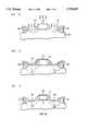
- FIGS. 1A-1Cillustrate a prior art self-aligned cobalt silicide processing sequence by cross-sectional elevation view of a silicon substrate with a layer of thin oxide and a layer of cobalt silicide formed thereon.
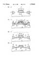
- FIGS. 3A-3Dillustrate an embodiment of the present invention in which the self-aligned cobalt silicide processing sequence of the present invention is used in the fabrication of an n-MOSFET device.
- FIGS. 4A-4Dillustrate an embodiment of the present invention in which the self-aligned cobalt silicide processing sequence of the present invention is used in the fabrication of an n-MOSFET device in which the cobalt silicide is used as a doping source.
- the present inventionis directed to a process for forming an epitaxial quality cobalt silicide (CoSi 2 ) layer for use in self aligned silicon technology.
- the processis incorporated into processes for device fabrication in which a layer of cobalt silicide is desired.
- processes in which the present invention is incorporatedinclude processes in which an epitaxial CoSi 2 layer in heavily-doped diffused regions of a Si MOSFET device is desired and processes that use a CoSi 2 layer as a diffusion source.
- FIGS. 2A-2Care a schematic illustration of a cross-section of a silicon substrate on which a layer of CoSi 2 is formed according to the process of the present invention.
- a thin layeri.e. a thickness of 0.5 to about 1.5 nm or less
- oxide 200is formed by conventional methods such as by subjecting the substrate to a chemical cleaning solution known to form oxide on exposed silicon surfaces. These chemical solutions typically contain hydrogen peroxide and water.
- suitable solutionsinclude solutions of hot (e.g., about 100° C.) hydrochloric acid (HCl) and hydrogen peroxide (H 2 O 2 ) in water (a 3:1:1 by volume solution) and hot (e.g., about 90° C.) ammonium hydroxide (NH 4 OH) and H 2 O 2 in water (a 1:1:4 by volume solution).
- the substrateis submerged in the solution for about 5 to about 20 minutes.
- a suitable method for growing the oxide layeris annealing the silicon substrate in a dry oxygen atmosphere under conditions sufficient to grow an oxide layer with a maximum thickness of about 1.5 nm.
- suitable conditionsis an anneal at 810° C. in pure oxygen for about 4 minutes.
- the waferis placed in an environment that is essentially oxygen-free.
- oxygenis excluded from the environment to prevent the cobalt from oxidizing to a significant degree during the subsequent annealing steps.
- Suitable environmentsinclude vacuum environments and inert atmospheres such as Argon.
- the substratesare then subjected to conditions for forming a layer of cobalt 220 on the surface of the substrate 210.
- the cobalt layer 220is formed over the oxide layer 200.
- the conditionsare selected so that the cobalt layer has a uniform thickness.
- the cobalt layer 220is formed on the surface of the substrate using conventional techniques such as e-beam evaporation or sputter deposition. It is advantageous if e-beam evaporation is used to form the cobalt on the surface of the substrate because the resulting cobalt layer is uniform and relatively free of impurities.
- the thickness of the cobalt layeris greater than 1 nm and does not exceed about 5 nm, In order to obtain the desired layer uniformity, it is advantageous if the thickness of the cobalt is less than 4 nm.
- the resulting CoSi 2 layers formed by the process of the present inventionare observed to be inhomogeneous if the cobalt layers formed on the substrate are not within the prescribed thickness range.
- the substrateis then annealed.
- the substrateis kept in an essentially oxygen free environment until after the annealing step.
- the temperature at which the substrate is annealedis largely a matter of design choice. However, it is advantageous if the temperature is between about 450° C. and about 800° C.
- the substrateis annealed for an amount of time that is sufficient to convert the cobalt to cobalt silicide.
- the amount of timeis a function of the thickness of the cobalt layer and the temperature at which the anneal takes place. For example, a 30 second anneal is sufficient to convert a 2 nm-thick layer of cobalt to cobalt silicide at 600° C.
- cobalt silicide 225is formed directly over the silicon substrate 210 and the oxide layer 200 then overlies the cobalt silicide layer 225. Since the thickness of the cobalt layer formed on the substrate has a thickness of about 1 nm to about 5 nm, the thickness of the resulting, fully reacted, CoSi 2 layer is about 3.6 nm to about 18 nm. In certain instances, CoSi 2 layers with a thickness greater than about 18 nm is desired.
- Thicker CoSi 2 layersare formed by repeating the process sequence described above, i.e., a layer of cobalt is formed on the surface of the substrate and annealed to form CoSi 2 while the substrate is maintained in an essentially oxygen-free environment.
- a layer of cobaltis formed on the surface of the substrate and annealed to form CoSi 2 while the substrate is maintained in an essentially oxygen-free environment.
- the substrateis maintained in an essentially oxygen-free environment until the entire CoSi 2 layer is formed.
- These subsequent layers of cobaltare not limited in thickness in the same manner as the initial cobalt layer. However, it is advantageous if the thickness of the subsequent cobalt layers does not exceed about one-third the thickness of the underlying cobalt silicide.
- This limitation on the thickness of the cobalt layersis to prevent the renucleation of CoSi 2 in subsequent silicide reactions.
- This thickness limitation on the subsequent layers of cobalt formed over the initial cobalt silicide layerensures that the amount of existing CoSi 2 is adequate to accommodate the Co 2 Si and CoSi reactions with the subsequent cobalt layer.
- a field insulating film 301such as SiO 2
- a gate electrode 308is formed.
- the gate electrode 308,is formed using conventional processing techniques.
- a gate insulating film 303such as a thermally grown SiO 2 film, is formed on the surface of active regions between the field insulating portions 301.
- a polycrystalline silicon film 304is formed on the surface of the gate insulating film by a CVD (chemical vapor deposition) process, after which a WSi x layer 305 is sputtered on top of the polycrystalline Si layer 304.
- An n-type dopantsuch as As, is then implanted into the WSi x layer 305 and the upper part of the polycrystalline silicon (Si) layer 304.
- a hard mask layer 307such as an SiO 2 layer, is then deposited on the WSi x layer and the stack of hard mask 307, WSi x layer 305 and the polycrystalline Si layer 304 is then etched in a desired pattern to form the gate electrode 308 atop the gate insulating film 303 depicted in FIG. 3A.
- n-type impuritiesare then implanted at low concentration into the Si substrate, with the gate electrode 308 acting as a mask, after which a further SiO 2 film 309 is deposited over the gate electrode 304 and the gate insulating film 303.
- This SiO 2 film 309is anisotropically etched vertically and horizontally relative to the substrate 302 by a reactive ion etching (RIE) process to form the side wall spacers 309 on the sides of the gate electrode 304.
- RIEreactive ion etching
- n-type impuritiessuch as arsenic (As) are implanted at high concentration into the silicon substrate 301 with the gate electrode 308 and the side wall spacers 309 acting as a mask.
- the deviceis then annealed to electrically activate the implanted impurities and hence dope the polycrystalline silicon 304 and form the shallow junctions in the source 311 and drain 312 region with lightly doped extensions.
- a dilute, HF-containing, aqueous solutionis then used to remove any native oxide on the surface of the source 311 and drain 312 regions and any of the gate insulating film 303 that remains in the source 311 and drain 312 regions. Small portions of the side wall and the hard mask material are also removed during the HF etch.
- the waferis then immersed in a 1:1:4 solution of H 2 O 2 :NH 4 OH:H 2 O at 90° C. for 15 minutes to grow a thin SiO x layer 315 in the heavily-doped source 311 and drain 312 areas.
- the wafer 300is then loaded in a sputtering chamber with a low background (e.g., less than about 5 ⁇ 10 -9 torr) of oxygen, water vapor, and hydrocarbon partial pressures.
- a uniform layer of high-purity cobalt 320, 2.5 nm thick,is then sputtered at a low deposition rate (less than about 0.5 nm/s) while the wafer is maintained at 300° C.
- this cobalt layer 320is annealed in the oxygen-free sputtering chamber at 650° C. for 2 minutes which leads to the growth of an epitaxial CoSi 2 layer 325 on top of the source 311 and drain 312 regions.
- a second uniform layer of cobalt 330, 2 nm thick,is then sputtered while the substrate is held at less than 300° C., resulting in the structure depicted in FIG. 3C.
- a second anneal in the essentially oxygen-free sputtering chamber at 700° C. for 1 minutefollows, which increases the thickness of the epitaxial CoSi 2 layer 325.
- a wet etchis then used to remove unreacted cobalt (320 and 330) from atop the field oxide, the hard mask and the side walls.
- the waferis annealed at 850° C. for 1 minute in a nitrogen ambient. During this anneal, the SiO x layer 315 evaporates and/or agglomerates.
- FIG. 3Dillustrates that the cobalt silicide 325 remains in the source and drain regions of the substrate 302.
- the epitaxial CoSi 2 formed in the source and drain regionshas a thickness of about 16 nm.
- the technique of silicide as doping sourceis used to form the shallow junction.
- a field insulating film 401such as SiO 2 is selectively formed on portions of a lightly doped p-type Si substrate 402, for isolation between various elements.
- a gate insulating film 403, such as a thermally grown SiO 2 filmis formed on the surface of an active region between the field insulating portions 401.
- a polycrystalline silicon film 404is formed on the surface of the gate insulating film 403 by a CVD (chemical vapor deposition) process, after which a WSi x layer 405 is sputtered on top of the polycrystalline Si layer 404.
- the stack containing the hard mask 407, the WSi x layer 405, and the polycrystalline Si layer 404is then etched in a desired pattern to form the gate electrode 408 atop the gate insulating film 403.
- SiO 2 film 415is deposited over the gate electrode 408 and the gate insulating film 403. This SiO 2 film 415 is subjected to anisotropic etching vertically and horizontally relative to the substrate 401 by a reactive ion etching (RIE) process to form the side wall spacers 415 on the sides of the gate electrode 408 as shown in FIG. 4A.
- RIEreactive ion etching
- a dilute, HF-containing, aqueous solutionis first used to remove the gate insulating film 403 and the native oxide over the source 411 and drain 412 regions. Small portions of the side wall 415 and the hard mask 407 are also removed during the HF etch. The wafer is then immersed in a 1:3:1 solution of H 2 O 2 :HCl:H 2 O solution at about 100° C. for 5 minutes to grow a thin SiO x layer 425 in the source 411 and drain 412 areas.
- the waferis then loaded in a ultra-high vacuum evaporation chamber with low background oxygen, water vapor, and hydrocarbon partial pressures less than about 1 ⁇ 10 -10 torr.
- a uniform layer of high purity cobalt 435, 2.5 nm thick,is e-beam deposited at a low deposition rate (i.e. less than 0.5 nm/s) while the substrate is held at room temperature.
- the substrate with cobalt layer 435 formed thereonis annealed in an ultra high vacuum (UHV) evaporation chamber at 600° C. for 2 minutes, leading to the growth of epitaxial CoSi 2 layer 430 in the source 411 and drain 412 regions.
- UHVultra high vacuum
- the portion of the cobalt layer 435 on top of the field insulating layer 401, the spacer 415, and the hard mask 407does not react to form cobalt silicide as indicated in FIG. 4B by the fact that the cobalt 435 remains on top of the substrate in these regions.
- a second uniform layer of cobalt 440, 2 nm thick,is then e-beam deposited while the wafer is held at a temperature less than 300° C.
- a second anneal in the UHV evaporation chamber at 700° C. for 1 minutefollows. After unreacted cobalt is removed from atop the field oxide 401, the hard mask 407 and the side walls 415 through a wet etching, the wafer is annealed at 850° C. for 1 minute in a nitrogen ambient. The thin SiO 2 layer 425 either dissolves or agglomerates during this anneal.
- n-type impuritiessuch as arsenic (As) are implanted at high concentration into the epitaxial CoSi 2 layer 430 as shown in FIG. 4C.
- the substrateis annealed at about 900° C. for 5 minutes to allow arsenic to diffuse out of the CoSi 2 layers and into the single crystal Si area immediately surrounding the CoSi 2 layer and form heavily doped n + regions 450 and 460, as illustrated in FIG. 4D.
- n-type dopantsdiffuse into the polycrystalline Si layer 404.
- silicon substrateswere obtained. These substrates were Si(100), Si(110), Si(111), Si(511), Si(211), 4°-misoriented Si(100) substrates, Si(100) substrates implanted with arsenic (As) dopants, Si(100) substrates implanted with boron (BF 2 ) dopants, and oxide patterned Si(100) substrates.
- the As-implanted substrateshad a dose of 3 ⁇ 10 15 cm -2 at an implant energy of 70 keV.
- the BF 2 -implanted substrateshad a dose of 3 ⁇ 10 15 cm -2 at an implant energy of 40 keV.
- the implanted waferswere annealed at 1000° C. for 10 seconds in nitrogen after the implant.
- the substrateswere then subjected to one of two methods for growing a thin oxide layer on the surface of the substrate.
- the first methodwas by immersing a wafer in a hot solution of HCl:H 2 O 2 :H 2 O (3:1:1 solution) for 5 minutes.
- the second methodwas by immersing a wafer in a hot solution of NH 4 OH:H 2 O 2 :H 2 O (1:1:4 solution) for 20 minutes.
- An oxide layer with a thickness of about 0.5 to about 1.5 nmwas formed on the various substrates using the above-described methods.
- the substrateswere then placed in a UHV system with a base pressure of 6 ⁇ 10 -11 torr and equipped with an electron beam evaporator. Cobalt was evaporated on the unheated substrates to a thickness of 2 nm at a deposition rate of 0.05 nm/sec. The chamber pressure was maintained below 2 ⁇ 10 -10 torr during evaporation. Substrates were then annealed in the evaporation chamber at 650° C. for two minutes. A second layer of Co, 1.5 nm thick, was then evaporated onto the unheated substrates at the same rate of 0.05 nm/sec. The substrates were then annealed at 650° C. for two minutes.
- the substrateswere then annealed at 700° C. for one minute.
- the substrateswere then removed from the vacuum chamber and immersed in a selective Co etch (a 16:1:1:2 solution of phosphoric acid, nitric acid, acetic acid and water, by volume, respectively, was used) at room temperature for two minutes. After the substrates were rinsed in deionized water and dried, the substrates were annealed at 850° C. for one minute in nitrogen.
- the thickness of the uniform, epitaxial CoSi 2 layer on the substrateswas about 23 nm.
Landscapes
- Engineering & Computer Science (AREA)
- Physics & Mathematics (AREA)
- Condensed Matter Physics & Semiconductors (AREA)
- General Physics & Mathematics (AREA)
- Manufacturing & Machinery (AREA)
- Computer Hardware Design (AREA)
- Microelectronics & Electronic Packaging (AREA)
- Power Engineering (AREA)
- Electrodes Of Semiconductors (AREA)
- Insulated Gate Type Field-Effect Transistor (AREA)
Abstract
Description
Claims (18)
Priority Applications (4)
| Application Number | Priority Date | Filing Date | Title |
|---|---|---|---|
| US08/627,560US5728625A (en) | 1996-04-04 | 1996-04-04 | Process for device fabrication in which a thin layer of cobalt silicide is formed |
| DE69724317TDE69724317T2 (en) | 1996-04-04 | 1997-03-25 | Device manufacturing method in which a thin cobalt silicide layer is formed |
| EP97302049AEP0800204B1 (en) | 1996-04-04 | 1997-03-25 | A process for device fabrication in which a thin layer of cobalt silicide is formed |
| JP08544297AJP3600399B2 (en) | 1996-04-04 | 1997-04-04 | Fabrication process for devices with thin layers of cobalt silicide |
Applications Claiming Priority (1)
| Application Number | Priority Date | Filing Date | Title |
|---|---|---|---|
| US08/627,560US5728625A (en) | 1996-04-04 | 1996-04-04 | Process for device fabrication in which a thin layer of cobalt silicide is formed |
Publications (1)
| Publication Number | Publication Date |
|---|---|
| US5728625Atrue US5728625A (en) | 1998-03-17 |
Family
ID=24515162
Family Applications (1)
| Application Number | Title | Priority Date | Filing Date |
|---|---|---|---|
| US08/627,560Expired - LifetimeUS5728625A (en) | 1996-04-04 | 1996-04-04 | Process for device fabrication in which a thin layer of cobalt silicide is formed |
Country Status (4)
| Country | Link |
|---|---|
| US (1) | US5728625A (en) |
| EP (1) | EP0800204B1 (en) |
| JP (1) | JP3600399B2 (en) |
| DE (1) | DE69724317T2 (en) |
Cited By (41)
| Publication number | Priority date | Publication date | Assignee | Title |
|---|---|---|---|---|
| US6071782A (en)* | 1998-02-13 | 2000-06-06 | Sharp Laboratories Of America, Inc. | Partial silicidation method to form shallow source/drain junctions |
| US6087254A (en)* | 1996-07-16 | 2000-07-11 | Micron Technology, Inc. | Technique for elimination of pitting on silicon substrate during gate stack etch |
| US6153484A (en)* | 1995-06-19 | 2000-11-28 | Imec Vzw | Etching process of CoSi2 layers |
| US6221766B1 (en) | 1997-01-24 | 2001-04-24 | Steag Rtp Systems, Inc. | Method and apparatus for processing refractory metals on semiconductor substrates |
| US6255179B1 (en) | 1999-08-04 | 2001-07-03 | International Business Machines Corporation | Plasma etch pre-silicide clean |
| US6277743B1 (en)* | 1998-06-25 | 2001-08-21 | Texas Instruments Incorporated | Method of fabricating self-aligned silicide |
| US6281117B1 (en) | 1999-10-25 | 2001-08-28 | Chartered Semiconductor Manufacturing Ltd. | Method to form uniform silicide features |
| US6300206B1 (en)* | 1997-09-19 | 2001-10-09 | Hitachi, Ltd. | Method for manufacturing semiconductor device |
| US20010028087A1 (en)* | 2000-04-06 | 2001-10-11 | Norio Hirashita | Structure of a field effect transistor having metallic silicide and manufacturing method thereof |
| US6319784B1 (en)* | 1999-05-26 | 2001-11-20 | Taiwan Semiconductor Manufacturing Company | Using high temperature H2 anneal to recrystallize S/D and remove native oxide simultaneously |
| US6340627B1 (en) | 1996-10-29 | 2002-01-22 | Micron Technology, Inc. | Method of making a doped silicon diffusion barrier region |
| US6410429B1 (en) | 2001-03-01 | 2002-06-25 | Chartered Semiconductor Manufacturing Inc. | Method for fabricating void-free epitaxial-CoSi2 with ultra-shallow junctions |
| US6436818B1 (en) | 1997-02-19 | 2002-08-20 | Micron Technology, Inc. | Semiconductor structure having a doped conductive layer |
| US6445045B2 (en) | 1997-02-19 | 2002-09-03 | Micron Technology, Inc. | Low resistivity titanium silicide structures |
| US20030001212A1 (en)* | 1997-02-19 | 2003-01-02 | Micron Technology, Inc. | Conductor layer nitridation |
| US6518107B2 (en)* | 2001-02-16 | 2003-02-11 | Advanced Micro Devices, Inc. | Non-arsenic N-type dopant implantation for improved source/drain interfaces with nickel silicides |
| US20030030117A1 (en)* | 2001-05-22 | 2003-02-13 | Hitachi, Ltd. | Semiconductor device |
| US6545326B2 (en) | 1997-09-19 | 2003-04-08 | Hitachi, Ltd. | Method of fabricating semiconductor device |
| US6544890B2 (en)* | 1999-02-26 | 2003-04-08 | Nec Corporation | Process for fabricating semiconductor device having silicide layer with low resistance and uniform profile and sputtering system used therein |
| US20030145780A1 (en)* | 2002-02-07 | 2003-08-07 | Wacker Siltronic Ag | Silicon single crystal and process for producing it |
| US6610564B2 (en) | 2000-03-03 | 2003-08-26 | Shinichi Fukada | Method of fabricating semiconductor device |
| US6613673B2 (en) | 1996-07-16 | 2003-09-02 | Micron Technology, Inc. | Technique for elimination of pitting on silicon substrate during gate stack etch |
| US6627543B1 (en) | 2000-05-03 | 2003-09-30 | Integrated Device Technology, Inc. | Low-temperature sputtering system and method for salicide process |
| US6649520B1 (en)* | 1999-06-16 | 2003-11-18 | Hynix Semiconductor, Inc. | Method of forming film for reduced ohmic contact resistance and ternary phase layer amorphous diffusion barrier |
| US6765269B2 (en) | 2001-01-26 | 2004-07-20 | Integrated Device Technology, Inc. | Conformal surface silicide strap on spacer and method of making same |
| US6849543B2 (en)* | 2002-10-12 | 2005-02-01 | Taiwan Semiconductor Manufacturing Co., Ltd | Cobalt silicide formation method employing wet chemical silicon substrate oxidation |
| US20060057761A1 (en)* | 2003-04-25 | 2006-03-16 | Fujitsu Limited | Method for fabricating microstructure and microstructure |
| US20060057853A1 (en)* | 2004-09-15 | 2006-03-16 | Manoj Mehrotra | Thermal oxidation for improved silicide formation |
| US7037371B1 (en)* | 1999-10-04 | 2006-05-02 | Matsushita Electric Industrial Co., Ltd. | Method for fabricating semiconductor device |
| US7041548B1 (en) | 1996-07-16 | 2006-05-09 | Micron Technology, Inc. | Methods of forming a gate stack that is void of silicon clusters within a metallic silicide film thereof |
| US7078342B1 (en) | 1996-07-16 | 2006-07-18 | Micron Technology, Inc. | Method of forming a gate stack |
| US20060223296A1 (en)* | 2004-07-14 | 2006-10-05 | Sun Min-Chul | Semiconductor device having self-aligned silicide layer and method thereof |
| US7151020B1 (en)* | 2004-05-04 | 2006-12-19 | Advanced Micro Devices, Inc. | Conversion of transition metal to silicide through back end processing in integrated circuit technology |
| US20080124925A1 (en)* | 2006-09-25 | 2008-05-29 | International Business Machines Corporation | Method for improved formation of cobalt silicide contacts in semiconductor devices |
| US20110065976A1 (en)* | 2009-09-14 | 2011-03-17 | Minnesota Medical Physics Llc | Thermally assisted pulsed electro-magnetic field stimulation device and method for treatment of osteoarthritis |
| CN102184946A (en)* | 2011-03-17 | 2011-09-14 | 复旦大学 | Metal semiconductor compound film, DRAM (Dynamic Random Access Memory) storage unit and preparation method thereof |
| US20120139047A1 (en)* | 2010-11-29 | 2012-06-07 | Jun Luo | Semiconductor device and method of manufacturing the same |
| CN103390549A (en)* | 2012-05-11 | 2013-11-13 | 中国科学院微电子研究所 | Semiconductor device manufacturing method |
| RU2530456C1 (en)* | 2013-03-06 | 2014-10-10 | Федеральное государственное бюджетное учреждение наук Институт автоматики и процессов управления Дальневосточного отделения Российской академии наук (ИАПУ ДВО РАН) | Method for production of layered nanomaterial |
| CN104672877A (en)* | 2013-11-27 | 2015-06-03 | 三星Sdi株式会社 | Thermoplastic Resin Composition And Molded Article Including The Same |
| CN110164756A (en)* | 2019-05-30 | 2019-08-23 | 上海华虹宏力半导体制造有限公司 | A kind of preparation method of polysilicon membrane |
Families Citing this family (8)
| Publication number | Priority date | Publication date | Assignee | Title |
|---|---|---|---|---|
| JPH1145995A (en)* | 1997-07-25 | 1999-02-16 | Nec Kyushu Ltd | Semiconductor device and manufacturing method thereof |
| TW465024B (en)* | 1997-12-29 | 2001-11-21 | Lg Semicon Co Ltd | Semiconductor device fabrication method |
| JP3295931B2 (en)* | 1999-04-28 | 2002-06-24 | 日本電気株式会社 | Method for manufacturing semiconductor device |
| US6569766B1 (en) | 1999-04-28 | 2003-05-27 | Nec Electronics Corporation | Method for forming a silicide of metal with a high melting point in a semiconductor device |
| US6251779B1 (en)* | 2000-06-01 | 2001-06-26 | United Microelectronics Corp. | Method of forming a self-aligned silicide on a semiconductor wafer |
| US7005376B2 (en)* | 2003-07-07 | 2006-02-28 | Advanced Micro Devices, Inc. | Ultra-uniform silicides in integrated circuit technology |
| US7575959B2 (en)* | 2004-11-26 | 2009-08-18 | Semiconductor Energy Laboratory Co., Ltd. | Manufacturing method of semiconductor device |
| DE102012003585A1 (en)* | 2012-02-27 | 2013-08-29 | Forschungszentrum Jülich GmbH | Process for producing a monocrystalline metal-semiconductor compound |
Citations (8)
| Publication number | Priority date | Publication date | Assignee | Title |
|---|---|---|---|---|
| US5047367A (en)* | 1990-06-08 | 1991-09-10 | Intel Corporation | Process for formation of a self aligned titanium nitride/cobalt silicide bilayer |
| US5194405A (en)* | 1989-07-06 | 1993-03-16 | Sony Corporation | Method of manufacturing a semiconductor device having a silicide layer |
| US5266156A (en)* | 1992-06-25 | 1993-11-30 | Digital Equipment Corporation | Methods of forming a local interconnect and a high resistor polysilicon load by reacting cobalt with polysilicon |
| US5290731A (en)* | 1991-03-07 | 1994-03-01 | Sony Corporation | Aluminum metallization method |
| US5308793A (en)* | 1991-07-24 | 1994-05-03 | Sony Corporation | Method for forming interconnector |
| US5397744A (en)* | 1991-02-19 | 1995-03-14 | Sony Corporation | Aluminum metallization method |
| US5399526A (en)* | 1991-06-28 | 1995-03-21 | Sony Corporation | Method of manufacturing semiconductor device by forming barrier metal layer between substrate and wiring layer |
| US5563100A (en)* | 1993-12-16 | 1996-10-08 | Nec Corporation | Fabrication method of semiconductor device with refractory metal silicide formation by removing native oxide in hydrogen |
Family Cites Families (3)
| Publication number | Priority date | Publication date | Assignee | Title |
|---|---|---|---|---|
| US4492971A (en)* | 1980-06-05 | 1985-01-08 | At&T Bell Laboratories | Metal silicide-silicon heterostructures |
| US4477308A (en)* | 1982-09-30 | 1984-10-16 | At&T Bell Laboratories | Heteroepitaxy of multiconstituent material by means of a _template layer |
| US4707197A (en)* | 1984-08-02 | 1987-11-17 | American Telephone And Telegraph Company, At&T Bell Laboratories | Method of producing a silicide/Si heteroepitaxial structure, and articles produced by the method |
- 1996
- 1996-04-04USUS08/627,560patent/US5728625A/ennot_activeExpired - Lifetime
- 1997
- 1997-03-25EPEP97302049Apatent/EP0800204B1/ennot_activeExpired - Lifetime
- 1997-03-25DEDE69724317Tpatent/DE69724317T2/ennot_activeExpired - Lifetime
- 1997-04-04JPJP08544297Apatent/JP3600399B2/ennot_activeExpired - Lifetime
Patent Citations (8)
| Publication number | Priority date | Publication date | Assignee | Title |
|---|---|---|---|---|
| US5194405A (en)* | 1989-07-06 | 1993-03-16 | Sony Corporation | Method of manufacturing a semiconductor device having a silicide layer |
| US5047367A (en)* | 1990-06-08 | 1991-09-10 | Intel Corporation | Process for formation of a self aligned titanium nitride/cobalt silicide bilayer |
| US5397744A (en)* | 1991-02-19 | 1995-03-14 | Sony Corporation | Aluminum metallization method |
| US5290731A (en)* | 1991-03-07 | 1994-03-01 | Sony Corporation | Aluminum metallization method |
| US5399526A (en)* | 1991-06-28 | 1995-03-21 | Sony Corporation | Method of manufacturing semiconductor device by forming barrier metal layer between substrate and wiring layer |
| US5308793A (en)* | 1991-07-24 | 1994-05-03 | Sony Corporation | Method for forming interconnector |
| US5266156A (en)* | 1992-06-25 | 1993-11-30 | Digital Equipment Corporation | Methods of forming a local interconnect and a high resistor polysilicon load by reacting cobalt with polysilicon |
| US5563100A (en)* | 1993-12-16 | 1996-10-08 | Nec Corporation | Fabrication method of semiconductor device with refractory metal silicide formation by removing native oxide in hydrogen |
Non-Patent Citations (6)
| Title |
|---|
| "A Manufacturable Process for the Formation of Self Aligned Cobalt Silicide in a Sub Micrometer CMOS Technology", Berti, A.C.,1992 Proc. 9th International VLSI Multilevel Interconnection Conference(VMIC), pp. 267-273, (Jun. 9-10, 1992). |
| "New Silicidation Technology by SITOX (Silicidation Through Oxide", by Sumi, H. et al., IEEE, IEDM Tech Dig., Dec. 1990, pp. 249-252. |
| A Manufacturable Process for the Formation of Self Aligned Cobalt Silicide in a Sub Micrometer CMOS Technology , Berti, A.C., 1992 Proc. 9th International VLSI Multilevel Interconnection Conference (VMIC), pp. 267 273, (Jun. 9 10, 1992).* |
| CoSi 2 An Attractive Alternative to TiSi 2 , by Maex, K., Semiconductor International, pp. 75 80, (Mar. 1995).* |
| CoSi2 "An Attractive Alternative to TiSi2", by Maex, K., Semiconductor International,pp. 75-80, (Mar. 1995). |
| New Silicidation Technology by SITOX (Silicidation Through Oxide , by Sumi, H. et al., IEEE, IEDM Tech Dig., Dec. 1990, pp. 249 252.* |
Cited By (77)
| Publication number | Priority date | Publication date | Assignee | Title |
|---|---|---|---|---|
| US6153484A (en)* | 1995-06-19 | 2000-11-28 | Imec Vzw | Etching process of CoSi2 layers |
| US6087254A (en)* | 1996-07-16 | 2000-07-11 | Micron Technology, Inc. | Technique for elimination of pitting on silicon substrate during gate stack etch |
| US7115492B2 (en) | 1996-07-16 | 2006-10-03 | Micron Technology, Inc. | Technique for elimination of pitting on silicon substrate during gate stack etch using material in a non-annealed state |
| US7078342B1 (en) | 1996-07-16 | 2006-07-18 | Micron Technology, Inc. | Method of forming a gate stack |
| US7041548B1 (en) | 1996-07-16 | 2006-05-09 | Micron Technology, Inc. | Methods of forming a gate stack that is void of silicon clusters within a metallic silicide film thereof |
| US6613673B2 (en) | 1996-07-16 | 2003-09-02 | Micron Technology, Inc. | Technique for elimination of pitting on silicon substrate during gate stack etch |
| US6340627B1 (en) | 1996-10-29 | 2002-01-22 | Micron Technology, Inc. | Method of making a doped silicon diffusion barrier region |
| US6744108B1 (en)* | 1996-10-29 | 2004-06-01 | Micron Technology, Inc. | Doped silicon diffusion barrier region |
| US6221766B1 (en) | 1997-01-24 | 2001-04-24 | Steag Rtp Systems, Inc. | Method and apparatus for processing refractory metals on semiconductor substrates |
| US20040238845A1 (en)* | 1997-02-19 | 2004-12-02 | Micron Technology. Inc. | Conductor layer nitridation |
| US6798026B2 (en) | 1997-02-19 | 2004-09-28 | Micron Technology, Inc. | Conductor layer nitridation |
| US6525384B2 (en) | 1997-02-19 | 2003-02-25 | Micron Technology, Inc. | Conductor layer nitridation |
| US6436818B1 (en) | 1997-02-19 | 2002-08-20 | Micron Technology, Inc. | Semiconductor structure having a doped conductive layer |
| US6445045B2 (en) | 1997-02-19 | 2002-09-03 | Micron Technology, Inc. | Low resistivity titanium silicide structures |
| US6444579B1 (en) | 1997-02-19 | 2002-09-03 | Micron Technology, Inc. | Methods of forming low resistivity titanium silicide structures |
| US20030001212A1 (en)* | 1997-02-19 | 2003-01-02 | Micron Technology, Inc. | Conductor layer nitridation |
| US6887774B2 (en) | 1997-02-19 | 2005-05-03 | Micron Technology, Inc. | Conductor layer nitridation |
| US20050239258A1 (en)* | 1997-09-19 | 2005-10-27 | Shinichi Fukada | Method of fabricating semiconductor device |
| US7118983B2 (en) | 1997-09-19 | 2006-10-10 | Renesas Technology Corp. | Method of fabricating semiconductor device |
| US6545326B2 (en) | 1997-09-19 | 2003-04-08 | Hitachi, Ltd. | Method of fabricating semiconductor device |
| US7074665B2 (en)* | 1997-09-19 | 2006-07-11 | Hitachi, Ltd. | Method of fabricating semiconductor device |
| US7569457B2 (en) | 1997-09-19 | 2009-08-04 | Renesas Technology Corp. | Method of fabricating semiconductor device |
| US20050250268A1 (en)* | 1997-09-19 | 2005-11-10 | Shinichi Fukada | Method of fabricating semiconductor device |
| US20080132022A1 (en)* | 1997-09-19 | 2008-06-05 | Shinichi Fukada | Method of fabricating semiconductor device |
| US7314805B2 (en) | 1997-09-19 | 2008-01-01 | Renesas Technology Corp. | Method for fabricating semiconductor device |
| US20050250269A1 (en)* | 1997-09-19 | 2005-11-10 | Shinichi Fukada | Method of fabricating semiconductor device |
| US20050186729A1 (en)* | 1997-09-19 | 2005-08-25 | Shinichi Fukada | Method of fabricating semiconductor device |
| US6300206B1 (en)* | 1997-09-19 | 2001-10-09 | Hitachi, Ltd. | Method for manufacturing semiconductor device |
| US20040092078A1 (en)* | 1997-09-19 | 2004-05-13 | Shinichi Fukada | Method of fabricating semiconductor device |
| US20070004163A1 (en)* | 1997-09-19 | 2007-01-04 | Shinichi Fukada | Method for fabricating semiconductor device |
| US7064040B2 (en) | 1997-09-19 | 2006-06-20 | Hitachi, Ltd. | Method of fabricating semiconductor device |
| US7094655B2 (en) | 1997-09-19 | 2006-08-22 | Renesas Technology Corp. | Method of fabricating semiconductor device |
| US7094642B2 (en)* | 1997-09-19 | 2006-08-22 | Hitachi, Ltd. | Method of fabricating semiconductor device |
| US6071782A (en)* | 1998-02-13 | 2000-06-06 | Sharp Laboratories Of America, Inc. | Partial silicidation method to form shallow source/drain junctions |
| US6277743B1 (en)* | 1998-06-25 | 2001-08-21 | Texas Instruments Incorporated | Method of fabricating self-aligned silicide |
| US6544890B2 (en)* | 1999-02-26 | 2003-04-08 | Nec Corporation | Process for fabricating semiconductor device having silicide layer with low resistance and uniform profile and sputtering system used therein |
| US6319784B1 (en)* | 1999-05-26 | 2001-11-20 | Taiwan Semiconductor Manufacturing Company | Using high temperature H2 anneal to recrystallize S/D and remove native oxide simultaneously |
| US6885103B2 (en) | 1999-06-16 | 2005-04-26 | Hyundai Electronics Industries Co., Ltd. | Semiconductor device including ternary phase diffusion barrier |
| US20040017010A1 (en)* | 1999-06-16 | 2004-01-29 | Hynix Semiconductor, Inc. | Method of forming film for reduced ohmic contact resistance and ternary phase layer amorphous diffusion barrier |
| US6649520B1 (en)* | 1999-06-16 | 2003-11-18 | Hynix Semiconductor, Inc. | Method of forming film for reduced ohmic contact resistance and ternary phase layer amorphous diffusion barrier |
| US6255179B1 (en) | 1999-08-04 | 2001-07-03 | International Business Machines Corporation | Plasma etch pre-silicide clean |
| US7037371B1 (en)* | 1999-10-04 | 2006-05-02 | Matsushita Electric Industrial Co., Ltd. | Method for fabricating semiconductor device |
| US6281117B1 (en) | 1999-10-25 | 2001-08-28 | Chartered Semiconductor Manufacturing Ltd. | Method to form uniform silicide features |
| US6670251B2 (en)* | 2000-03-03 | 2003-12-30 | Renesas Technology Corporation | Method of fabricating semiconductor device |
| US6610564B2 (en) | 2000-03-03 | 2003-08-26 | Shinichi Fukada | Method of fabricating semiconductor device |
| US20010028087A1 (en)* | 2000-04-06 | 2001-10-11 | Norio Hirashita | Structure of a field effect transistor having metallic silicide and manufacturing method thereof |
| US7479682B2 (en) | 2000-04-06 | 2009-01-20 | Oki Electric Industry Co., Ltd. | Structure of a field effect transistor having metallic silicide and manufacturing method thereof |
| US7244996B2 (en)* | 2000-04-06 | 2007-07-17 | Oki Electric Industry Co., Ltd. | Structure of a field effect transistor having metallic silicide and manufacturing method thereof |
| US20070158757A1 (en)* | 2000-04-06 | 2007-07-12 | Norio Hirashita | Structure of a field effect transistor having metallic silicide and manufacturing method thereof |
| US6627543B1 (en) | 2000-05-03 | 2003-09-30 | Integrated Device Technology, Inc. | Low-temperature sputtering system and method for salicide process |
| US6765269B2 (en) | 2001-01-26 | 2004-07-20 | Integrated Device Technology, Inc. | Conformal surface silicide strap on spacer and method of making same |
| US6518107B2 (en)* | 2001-02-16 | 2003-02-11 | Advanced Micro Devices, Inc. | Non-arsenic N-type dopant implantation for improved source/drain interfaces with nickel silicides |
| US6410429B1 (en) | 2001-03-01 | 2002-06-25 | Chartered Semiconductor Manufacturing Inc. | Method for fabricating void-free epitaxial-CoSi2 with ultra-shallow junctions |
| US7608899B2 (en) | 2001-05-22 | 2009-10-27 | Renesas Technology Corporation | Semiconductor device |
| US7217971B2 (en) | 2001-05-22 | 2007-05-15 | Hitachi, Ltd. | Miniaturized semiconductor device with improved dielectric properties |
| US20040217432A1 (en)* | 2001-05-22 | 2004-11-04 | Hitachi, Ltd. | Semiconductor device |
| US20030030117A1 (en)* | 2001-05-22 | 2003-02-13 | Hitachi, Ltd. | Semiconductor device |
| US20080061384A1 (en)* | 2001-05-22 | 2008-03-13 | Hitachi, Ltd. | Semiconductor Device |
| US7358578B2 (en) | 2001-05-22 | 2008-04-15 | Renesas Technology Corporation | Field effect transistor on a substrate with (111) orientation having zirconium oxide gate insulation and cobalt or nickel silicide wiring |
| US20030145780A1 (en)* | 2002-02-07 | 2003-08-07 | Wacker Siltronic Ag | Silicon single crystal and process for producing it |
| US20080210155A1 (en)* | 2002-02-07 | 2008-09-04 | Siltronic Ag | Silicon single crystal and process for producing it |
| US6849543B2 (en)* | 2002-10-12 | 2005-02-01 | Taiwan Semiconductor Manufacturing Co., Ltd | Cobalt silicide formation method employing wet chemical silicon substrate oxidation |
| US20060057761A1 (en)* | 2003-04-25 | 2006-03-16 | Fujitsu Limited | Method for fabricating microstructure and microstructure |
| US7833430B2 (en)* | 2003-04-25 | 2010-11-16 | Fujitsu Limited | Method for fabricating microstructure and microstructure |
| US7151020B1 (en)* | 2004-05-04 | 2006-12-19 | Advanced Micro Devices, Inc. | Conversion of transition metal to silicide through back end processing in integrated circuit technology |
| US20060223296A1 (en)* | 2004-07-14 | 2006-10-05 | Sun Min-Chul | Semiconductor device having self-aligned silicide layer and method thereof |
| US20060057853A1 (en)* | 2004-09-15 | 2006-03-16 | Manoj Mehrotra | Thermal oxidation for improved silicide formation |
| US20080124925A1 (en)* | 2006-09-25 | 2008-05-29 | International Business Machines Corporation | Method for improved formation of cobalt silicide contacts in semiconductor devices |
| US7485572B2 (en)* | 2006-09-25 | 2009-02-03 | International Business Machines Corporation | Method for improved formation of cobalt silicide contacts in semiconductor devices |
| US20110065976A1 (en)* | 2009-09-14 | 2011-03-17 | Minnesota Medical Physics Llc | Thermally assisted pulsed electro-magnetic field stimulation device and method for treatment of osteoarthritis |
| US20120139047A1 (en)* | 2010-11-29 | 2012-06-07 | Jun Luo | Semiconductor device and method of manufacturing the same |
| CN102184946A (en)* | 2011-03-17 | 2011-09-14 | 复旦大学 | Metal semiconductor compound film, DRAM (Dynamic Random Access Memory) storage unit and preparation method thereof |
| US20140008710A1 (en)* | 2011-03-17 | 2014-01-09 | Fudan University | Metal/Semiconductor Compound Thin Film and a DRAM Storage Cell and Method of Making |
| CN103390549A (en)* | 2012-05-11 | 2013-11-13 | 中国科学院微电子研究所 | Semiconductor device manufacturing method |
| RU2530456C1 (en)* | 2013-03-06 | 2014-10-10 | Федеральное государственное бюджетное учреждение наук Институт автоматики и процессов управления Дальневосточного отделения Российской академии наук (ИАПУ ДВО РАН) | Method for production of layered nanomaterial |
| CN104672877A (en)* | 2013-11-27 | 2015-06-03 | 三星Sdi株式会社 | Thermoplastic Resin Composition And Molded Article Including The Same |
| CN110164756A (en)* | 2019-05-30 | 2019-08-23 | 上海华虹宏力半导体制造有限公司 | A kind of preparation method of polysilicon membrane |
Also Published As
| Publication number | Publication date |
|---|---|
| JPH1027908A (en) | 1998-01-27 |
| EP0800204B1 (en) | 2003-08-27 |
| DE69724317T2 (en) | 2004-06-03 |
| EP0800204A2 (en) | 1997-10-08 |
| DE69724317D1 (en) | 2003-10-02 |
| JP3600399B2 (en) | 2004-12-15 |
| EP0800204A3 (en) | 1998-09-16 |
Similar Documents
| Publication | Publication Date | Title |
|---|---|---|
| US5728625A (en) | Process for device fabrication in which a thin layer of cobalt silicide is formed | |
| US5336903A (en) | Selective deposition of doped silicon-germanium alloy on semiconductor substrate, and resulting structures | |
| US6410427B1 (en) | Metal silicidation methods and methods for using same | |
| US5536684A (en) | Process for formation of epitaxial cobalt silicide and shallow junction of silicon | |
| JP3734559B2 (en) | Manufacturing method of semiconductor device | |
| US5795808A (en) | Method for forming shallow junction for semiconductor device | |
| JP3285934B2 (en) | Method for manufacturing semiconductor device | |
| US5281552A (en) | MOS fabrication process, including deposition of a boron-doped diffusion source layer | |
| US7030451B2 (en) | Method and apparatus for performing nickel salicidation | |
| US6329277B1 (en) | Method of forming cobalt silicide | |
| JPH07153717A (en) | Formation of silicide layer | |
| US5679585A (en) | Method for forming metal silicide on a semiconductor surface with minimal effect on pre-existing implants | |
| US6274511B1 (en) | Method of forming junction-leakage free metal silicide in a semiconductor wafer by amorphization of refractory metal layer | |
| US6461923B1 (en) | Sidewall spacer etch process for improved silicide formation | |
| JPH0878361A (en) | Manufacture of semiconductor device | |
| US6096599A (en) | Formation of junctions by diffusion from a doped film into and through a silicide during silicidation | |
| JP2956583B2 (en) | Semiconductor device and manufacturing method thereof | |
| US20060130746A1 (en) | Method for forming nickel silicide film, method for manufacturing semiconductor device, and method for etching nickel silicide | |
| US5858846A (en) | Salicide integration method | |
| US6486062B1 (en) | Selective deposition of amorphous silicon for formation of nickel silicide with smooth interface on N-doped substrate | |
| US6316362B1 (en) | Method for manufacturing semiconductor device | |
| KR100469221B1 (en) | A process for device fabrication in which a thin layer of cobalt silicide is formed | |
| JPH06196687A (en) | Manufacture of semiconductor device | |
| US6482737B2 (en) | Fabrication method of implanting silicon-ions into the silicon substrate | |
| JPH10135453A (en) | Semiconductor device and manufacturing method thereof |
Legal Events
| Date | Code | Title | Description |
|---|---|---|---|
| AS | Assignment | Owner name:LUCENT TECHNOLOGIES, INC., NEW JERSEY Free format text:ASSIGNMENT OF ASSIGNORS INTEREST;ASSIGNOR:TUNG, RAYMOND TZUTSE;REEL/FRAME:007981/0928 Effective date:19960404 | |
| FEPP | Fee payment procedure | Free format text:PAYOR NUMBER ASSIGNED (ORIGINAL EVENT CODE: ASPN); ENTITY STATUS OF PATENT OWNER: LARGE ENTITY | |
| STCF | Information on status: patent grant | Free format text:PATENTED CASE | |
| AS | Assignment | Owner name:CHASE MANHATTAN BANK, AS ADMINISTRATIVE AGENT, THE Free format text:CONDITIONAL ASSIGNMENT OF AND SECURITY INTEREST IN PATENT RIGHTS;ASSIGNOR:AGERE SYSTEMS GUARDIAN CORP. (DE CORPORATION);REEL/FRAME:011667/0148 Effective date:20010402 | |
| AS | Assignment | Owner name:AGERE SYSTEMS GUARDIAN CORP., FLORIDA Free format text:ASSIGNMENT OF ASSIGNORS INTEREST;ASSIGNOR:LUCENT TECHNOLOGIES INC.;REEL/FRAME:011796/0615 Effective date:20010131 | |
| FPAY | Fee payment | Year of fee payment:4 | |
| AS | Assignment | Owner name:AGERE SYSTEMS GUARDIAN CORP., FLORIDA Free format text:TERMINATION AND RELEASE OF SECURITY INTEREST IN PATENT RIGHTS;ASSIGNOR:JPMORGAN CHASE BANK (F/K/A THE CHASE MANHATTAN BANK);REEL/FRAME:013372/0662 Effective date:20020930 | |
| FPAY | Fee payment | Year of fee payment:8 | |
| FPAY | Fee payment | Year of fee payment:12 | |
| AS | Assignment | Owner name:DEUTSCHE BANK AG NEW YORK BRANCH, AS COLLATERAL AG Free format text:PATENT SECURITY AGREEMENT;ASSIGNORS:LSI CORPORATION;AGERE SYSTEMS LLC;REEL/FRAME:032856/0031 Effective date:20140506 | |
| AS | Assignment | Owner name:AVAGO TECHNOLOGIES GENERAL IP (SINGAPORE) PTE. LTD Free format text:ASSIGNMENT OF ASSIGNORS INTEREST;ASSIGNOR:AGERE SYSTEMS LLC;REEL/FRAME:035365/0634 Effective date:20140804 | |
| AS | Assignment | Owner name:LSI CORPORATION, CALIFORNIA Free format text:TERMINATION AND RELEASE OF SECURITY INTEREST IN PATENT RIGHTS (RELEASES RF 032856-0031);ASSIGNOR:DEUTSCHE BANK AG NEW YORK BRANCH, AS COLLATERAL AGENT;REEL/FRAME:037684/0039 Effective date:20160201 Owner name:AGERE SYSTEMS LLC, PENNSYLVANIA Free format text:TERMINATION AND RELEASE OF SECURITY INTEREST IN PATENT RIGHTS (RELEASES RF 032856-0031);ASSIGNOR:DEUTSCHE BANK AG NEW YORK BRANCH, AS COLLATERAL AGENT;REEL/FRAME:037684/0039 Effective date:20160201 | |
| AS | Assignment | Owner name:BANK OF AMERICA, N.A., AS COLLATERAL AGENT, NORTH CAROLINA Free format text:PATENT SECURITY AGREEMENT;ASSIGNOR:AVAGO TECHNOLOGIES GENERAL IP (SINGAPORE) PTE. LTD.;REEL/FRAME:037808/0001 Effective date:20160201 Owner name:BANK OF AMERICA, N.A., AS COLLATERAL AGENT, NORTH Free format text:PATENT SECURITY AGREEMENT;ASSIGNOR:AVAGO TECHNOLOGIES GENERAL IP (SINGAPORE) PTE. LTD.;REEL/FRAME:037808/0001 Effective date:20160201 | |
| AS | Assignment | Owner name:AVAGO TECHNOLOGIES GENERAL IP (SINGAPORE) PTE. LTD., SINGAPORE Free format text:TERMINATION AND RELEASE OF SECURITY INTEREST IN PATENTS;ASSIGNOR:BANK OF AMERICA, N.A., AS COLLATERAL AGENT;REEL/FRAME:041710/0001 Effective date:20170119 Owner name:AVAGO TECHNOLOGIES GENERAL IP (SINGAPORE) PTE. LTD Free format text:TERMINATION AND RELEASE OF SECURITY INTEREST IN PATENTS;ASSIGNOR:BANK OF AMERICA, N.A., AS COLLATERAL AGENT;REEL/FRAME:041710/0001 Effective date:20170119 | |
| AS | Assignment | Owner name:BELL SEMICONDUCTOR, LLC, ILLINOIS Free format text:ASSIGNMENT OF ASSIGNORS INTEREST;ASSIGNORS:AVAGO TECHNOLOGIES GENERAL IP (SINGAPORE) PTE. LTD.;BROADCOM CORPORATION;REEL/FRAME:044886/0608 Effective date:20171208 | |
| AS | Assignment | Owner name:CORTLAND CAPITAL MARKET SERVICES LLC, AS COLLATERA Free format text:SECURITY INTEREST;ASSIGNORS:HILCO PATENT ACQUISITION 56, LLC;BELL SEMICONDUCTOR, LLC;BELL NORTHERN RESEARCH, LLC;REEL/FRAME:045216/0020 Effective date:20180124 | |
| AS | Assignment | Owner name:BELL NORTHERN RESEARCH, LLC, ILLINOIS Free format text:RELEASE BY SECURED PARTY;ASSIGNOR:CORTLAND CAPITAL MARKET SERVICES LLC;REEL/FRAME:059720/0719 Effective date:20220401 Owner name:BELL SEMICONDUCTOR, LLC, ILLINOIS Free format text:RELEASE BY SECURED PARTY;ASSIGNOR:CORTLAND CAPITAL MARKET SERVICES LLC;REEL/FRAME:059720/0719 Effective date:20220401 Owner name:HILCO PATENT ACQUISITION 56, LLC, ILLINOIS Free format text:RELEASE BY SECURED PARTY;ASSIGNOR:CORTLAND CAPITAL MARKET SERVICES LLC;REEL/FRAME:059720/0719 Effective date:20220401 |