US5727229A - Method and apparatus for moving data in a parallel processor - Google Patents
Method and apparatus for moving data in a parallel processorDownload PDFInfo
- Publication number
- US5727229A US5727229AUS08/596,843US59684396AUS5727229AUS 5727229 AUS5727229 AUS 5727229AUS 59684396 AUS59684396 AUS 59684396AUS 5727229 AUS5727229 AUS 5727229A
- Authority
- US
- United States
- Prior art keywords
- vector
- bit
- elements
- data
- array
- Prior art date
- Legal status (The legal status is an assumption and is not a legal conclusion. Google has not performed a legal analysis and makes no representation as to the accuracy of the status listed.)
- Expired - Fee Related
Links
Images


Classifications
- G—PHYSICS
- G06—COMPUTING OR CALCULATING; COUNTING
- G06F—ELECTRIC DIGITAL DATA PROCESSING
- G06F9/00—Arrangements for program control, e.g. control units
- G06F9/06—Arrangements for program control, e.g. control units using stored programs, i.e. using an internal store of processing equipment to receive or retain programs
- G06F9/30—Arrangements for executing machine instructions, e.g. instruction decode
- G06F9/38—Concurrent instruction execution, e.g. pipeline or look ahead
- G06F9/3877—Concurrent instruction execution, e.g. pipeline or look ahead using a slave processor, e.g. coprocessor
- G06F9/3879—Concurrent instruction execution, e.g. pipeline or look ahead using a slave processor, e.g. coprocessor for non-native instruction execution, e.g. executing a command; for Java instruction set
- G—PHYSICS
- G06—COMPUTING OR CALCULATING; COUNTING
- G06F—ELECTRIC DIGITAL DATA PROCESSING
- G06F15/00—Digital computers in general; Data processing equipment in general
- G06F15/16—Combinations of two or more digital computers each having at least an arithmetic unit, a program unit and a register, e.g. for a simultaneous processing of several programs
- G06F15/163—Interprocessor communication
- G06F15/173—Interprocessor communication using an interconnection network, e.g. matrix, shuffle, pyramid, star, snowflake
- G—PHYSICS
- G06—COMPUTING OR CALCULATING; COUNTING
- G06F—ELECTRIC DIGITAL DATA PROCESSING
- G06F15/00—Digital computers in general; Data processing equipment in general
- G06F15/76—Architectures of general purpose stored program computers
- G06F15/80—Architectures of general purpose stored program computers comprising an array of processing units with common control, e.g. single instruction multiple data processors
- G06F15/8053—Vector processors
- G06F15/8092—Array of vector units
- G—PHYSICS
- G06—COMPUTING OR CALCULATING; COUNTING
- G06F—ELECTRIC DIGITAL DATA PROCESSING
- G06F9/00—Arrangements for program control, e.g. control units
- G06F9/06—Arrangements for program control, e.g. control units using stored programs, i.e. using an internal store of processing equipment to receive or retain programs
- G06F9/30—Arrangements for executing machine instructions, e.g. instruction decode
- G06F9/30003—Arrangements for executing specific machine instructions
- G06F9/30007—Arrangements for executing specific machine instructions to perform operations on data operands
- G06F9/30032—Movement instructions, e.g. MOVE, SHIFT, ROTATE, SHUFFLE
- G—PHYSICS
- G06—COMPUTING OR CALCULATING; COUNTING
- G06F—ELECTRIC DIGITAL DATA PROCESSING
- G06F9/00—Arrangements for program control, e.g. control units
- G06F9/06—Arrangements for program control, e.g. control units using stored programs, i.e. using an internal store of processing equipment to receive or retain programs
- G06F9/30—Arrangements for executing machine instructions, e.g. instruction decode
- G06F9/30003—Arrangements for executing specific machine instructions
- G06F9/30007—Arrangements for executing specific machine instructions to perform operations on data operands
- G06F9/30036—Instructions to perform operations on packed data, e.g. vector, tile or matrix operations
- G—PHYSICS
- G06—COMPUTING OR CALCULATING; COUNTING
- G06F—ELECTRIC DIGITAL DATA PROCESSING
- G06F9/00—Arrangements for program control, e.g. control units
- G06F9/06—Arrangements for program control, e.g. control units using stored programs, i.e. using an internal store of processing equipment to receive or retain programs
- G06F9/30—Arrangements for executing machine instructions, e.g. instruction decode
- G06F9/38—Concurrent instruction execution, e.g. pipeline or look ahead
- G06F9/3824—Operand accessing
Definitions
- the present inventionrelates in general to a data processing system, and more particularly to a method of moving data in a parallel processor.
- Fuzzy logic, neural networks, and other parallel, array oriented applicationsare becoming very popular and important in data processing. Most digital data processing systems today have not been designed with fuzzy logic, neural networks, and other parallel, array oriented applications specifically in mind. To illustrate the additional complexity and requirements of a parallel, array oriented processing system, herein generally referred to as a parallel system, it is helpful to first distinguish a non-array based processing system, herein generally referred to as a non-array based system.
- a non-array based systemtypically includes one or more data processors each having a single processing element generally referred to as a central processing unit (CPU).
- CPUcentral processing unit
- a non-array based systemwhich uses a single instruction to operate on a single piece of data is referred to as an SISD system.
- SISD systema single instruction affects a single CPU.
- Each CPUthen has at least one associated memory storage device used for status, control, or operand storage.
- a parallel processing systemtypically includes a host processor having multiple processing elements.
- a parallel systemis a single instruction multiple data system, referred to as an SIMD system.
- SIMD systema single instruction affects multiple processing elements.
- MIMDmultiple input multiple data system
- Parallel systemsinclude many combinations and configurations of processing elements. Structurally and functionally, parallel systems are more complicated and complex than non-array based systems.
- Parallel, array based processinghas many advantages over non-array based processing as parallel, array based operations are performed in parallel rather than in tandem. Thus, no single processing element operates individually, but rather operates as part of a system of processing elements.
- Parallel systemseffectively offer a more robust method of computing and data processing. There are considerable performance and cost benefits to be gained in designing data processing systems which are especially adapted and designed to meet the requirements of fuzzy logic, neural networks, digital signal processing, and other parallel, array oriented applications. It is necessary to consider the parallel nature of these parallel type processors and array based systems in order to design flexible, parallel, array based type instruction sets that are effective in parallel type data processing and operation.
- FIG. 1illustrates, in block diagram form, a parallel processing system 3 in accordance with one embodiment of the present invention
- FIG. 2illustrates, in block diagram form, a portion of vector engine 70 in accordance with one embodiment of the present invention
- FIG. 3illustrates, in block diagram form, a global pointer unit 49 in accordance with one embodiment of the present invention
- FIG. 4illustrates, in block diagram form, a portion of a processing element array 80 and a global register file 50 of a vector engine 70 in accordance with one embodiment of the present invention
- FIG. 5illustrates, in block diagram form, a control register in accordance with one embodiment of the present invention
- FIG. 6illustrates, in flow diagram form, a method of moving data from a processing element in accordance with one embodiment of the present invention.
- FIG. 7illustrates, in flow diagram form, a method of moving data to a processing element in accordance with one embodiment of the present invention.
- the present inventionis a method and apparatus for moving data in a parallel processing system.
- a single instructionaccesses one significant bit of information from each element in a processing element array and combines the bits into one designated location in a global register file.
- the ordering of bits in a vector location of a global register fileassociates each bit with an element of the processing element array.
- another single instructiondistinguishes significant bit information from a designated location in a global register file and transfers that information to an associated bit in storage circuits associated with a plurality of elements in a processing element array.
- a parallel processing system 3includes a parallel data processor 5 having host processor 7, vector engine 70, and interface circuitry 30.
- Host processor 7consists of a processor core 10, coupled to instruction cache 15 by bus 4 and coupled to data cache 20 by bus 8.
- Instruction cache 15, data cache 20, and interface circuitry 30are each coupled to communication bus 25 by way of bi-directional multiple conductors.
- Communication bus 25allows communication between host processor 7, interface circuitry 30, and vector engine 70.
- interface circuitry 30is any type of circuitry which allows communication between data processor 5 and other devices.
- vector engine 70data movement and operations within vector engine 70 are controlled by vector sequencer 45, which is bi-directionally coupled by multiple conductors to instruction cache 35 and to data cache 40.
- Instruction cache 35 and data cache 40are each coupled to communication bus 25 by way of bi-directional multiple conductors. Note that other embodiments allow uni-directional, bi-directional or a combination for conductors among instruction cache 35, data cache 40, vector sequencer 45, and communication bus 25.
- Vector engine 70communicates with other modules in parallel processing system 3 via communication bus 25, and further with other devices by way of interface circuitry 30. Flexibility allows vector engine 70 to function as an autonomous module within parallel processing system 3.
- vector engine 70consists of vector sequencer 45, network 65, processing element array 80 and global pointer unit 49. All of three communicate through two busses, namely a source bus (S-bus) 92 and a result bus (R-bus) 96.
- Vector sequencer 45, network 65, processing element array 80, and global pointer unit 49are each coupled to S-bus 92 by way of bi-directional multiple conductors.
- network 65, processing element array 80, and global pointer unit 49are each coupled to R-bus 96 by way of bi-directional multiple conductors.
- global pointer unit 49is a global data path unit.
- Vector sequencer 45controls data movement and operations within vector engine 70 by providing signals to network 65, processing element array 80, and global pointer unit 49.
- vector sequencer 45receives status signals from within vector engine 70 and affects control decisions accordingly.
- Instruction cache 35 and data cache 40are local within vector engine 70 and each communicate through communication bus 25 by way of bi-directional multiple conductors.
- internal communication bus 13couples processing element array 80 and global pointer unit 49.
- Network 65is directly coupled to processing element array 80.
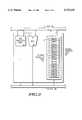
- processing element array 80is composed of sixteen processing elements PE(0) 60, PE(1) 61, PE(2) 62 through PE(14) 63, and PE(15) 64.
- Global pointer unit 49communicates with data cache 40 by way of bi-directional conductors.
- FIG.2illustrates a portion of vector engine 70 in one embodiment of the present invention, where processing element PE(0) 60 is exemplary of all processing elements PE(0) to PE(15) 64 in processing element array 80.
- PE(0) 60is analogous to an individual CPU, containing circuitry for data movement, control and status registers, memory storage locations, and logic circuitry.
- Vector sequencer 45provides decoded instructions, data, and control signals to PE(0) 60 through S-bus 92.
- multiple conductorsprovide data from S-bus 92 to control register VPCR(0) 81 and multiple conductors provide data from VPCR(0) 81 to R-bus 96.
- circuitry for data movement, mux/demux circuitry 85receives bit select signal 6 via a conductor from S-bus 92.
- control signalsare provided by mux/demux circuitry 85 to VPCR(0) 81 via bi-directional multiple conductors and logic operations are performed by arithmetic logic unit (ALU) 2, where ALU 2 receives inputs from S-bus 92 via two uni-directional conductors, and transmits an output to R-bus 96 by way of a uni-directional conductor.
- ALUarithmetic logic unit
- S-bus 92provides inputs to mux/demux circuitry 85, VPCR(0) 81, and ALU 2, while their outputs are directed to R-bus 96.
- Vector Register File 94receives input from R-bus 96 and provides output to S-bus 92. Uni-directional multiple conductors couple vector register file 94 to S-bus 92 and to R-bus 96.
- vector register file 94is a local memory storage unit, consisting of sixteen registers. Alternate embodiments may consist of any number of registers or memory storage units.
- decoded instructions, data, and control information from vector sequencer 45are provided to PE(0) 60 by way of S-bus 92, and output information, status information, and data from PE(0) 60 are provided to network 65 by way of R-bus 96.
- Global pointer unit 49illustrated in FIG. 3, is a local memory storage unit, within vector engine 70, for storing global information. Typically, global information is such that it may be accessed by various parts of vector engine 70 and parallel processing system 3.
- global pointer unit 49includes bit analysis unit 53, which receives inputs from S-bus 92 by way of uni-directional conductors, and provides an output to R-bus 96 by way of uni-directional multiple conductors.
- input to ALU 52is provided by way of uni-directional conductors from S-bus 92, while ALU 52 outputs to R-bus 96 by way of uni-directional conductors.
- global register file 50is an array of sixteen global registers or vectors, such as GREG(0) 51. Alternate embodiments include any number of global registers. Global register file 50 receives input from R-bus 96 by way of uni-directional conductors and provides output to S-bus 92 by way of uni-directional conductors. Note that alternate embodiments may use any number of conductors, bi-directional or uni-directional, to allow data and signal flow in global pointer unit 49 and processing elements PE(0) 60 to PE(15) 64.
- FIG.1illustrates an overall parallel processing system 3.
- FIG. 2focuses on an individual processing element, PE(0) 60, while FIG. 3 focuses on a global pointer unit 49.
- FIG. 4serves to illustrate data movement by considering a portion of processing element array 80, internal communication bus 13, and global register file 50, thus allowing a clear description of one embodiment of the present invention.
- global register file 50consists of sixteen vectors, such as GREG(0) 51.
- Global register file 50is a part of global pointer unit 49, which is coupled to internal communication bus 13 by way of bi-directional multiple conductors. Alternate embodiments may include one or any number of conductors.
- internal communication bus 13, which is coupled to processing element array 80 by way of bi-directional multiple conductors,serves as a communication path for data movement.
- processing element array 80is diagrammed as a vector array, typically, control vectors are contained within processing elements and are therefore physically separated.
- each processing element in processing element array 80has within it at least one memory vector and at least one control register.
- associated memory vectors VPE(0) 66, VPE(1) 67 through VPE(14) 68, VPE(15)69, and control registers VPCR(0) 81, VPCR(1) 82 through VPCR(14) 83, VPCR(15)84have index numbers which correspond to associated processing elements.
- "#N"indicates bit selection for data movement, (i.e.
- bit location "#N"is the object of the data movement.
- "#N”indicates bit selection of each vector in a portion of processing element array 80.
- "#N”is a selectable bit and can be any bit in associated memory vectors VPE(0) 66 to VPE(15)69, or control registers VPCR(0) 81 to VPCR(15)84. In alternate embodiments "#N" is a predetermined bit.
- global register, GREG(0) 51has sixteen bits, each bit having a significance to a corresponding processing element.
- data in bit location "#N" of VPCR(0) 81moves to least significant bit location (bit 0 or LSB) in GREG(0) 51.
- Data in bit location "#N” of VPCR(1) 82moves to the next sequential bit location (bit 1) in GREG(0)51.
- bit location "#N" of VPCR(n)moves to bit "n” of GREG(0) 51.
- global register GREG(0)is a compilation of data from bit location "#N" for all processing elements.
- control information for PE(0) 60is stored in VPCR(0), and includes vector signed overflow (OV) 99, vector carry (C) 98, vector conditional true (VT) 97, as well as thirteen reserved bits.
- the present inventionoffers a data movement to compile specific bit information from each of a plurality of processing elements into a single memory location. Additionally, the present invention offers a method of moving data from a single memory location to a specific bit location for each of a plurality of processing elements.
- FIGS. 6-7illustrate in flow diagram form, a method for performing data movement in vector engine 70.
- Flattened ovals 100 and 200represent starting points, while 140 and 240 represent ending points for each instruction.
- Rectangles 105, 110, 115, 120, 125, 205, 210, 215, 220, and 225represent control steps.
- Rectangles 130, 135, 230, and 235represent data movement steps.
- buswill be used to refer to a plurality of signals or conductors which may be used to transfer one or more various types of information, such as data, addresses, control, or status.
- assertand “negate” will be used when referring to the rendering of a signal, status bit, or similar apparatus into its logically true or logically false state, respectively. If the logically true state is a logic level one, the logically false state will be a logic level zero. And if the logically true state is a logic level zero, the logically false state will be a logic level one.
- each processing elementwill be given an associated index number "n", which will be a suffix.
- PE(n)In processing element array 80, there are sixteen processing elements, the third PE being referred to as PE(2) 62.
- each component within a given PEis assigned the same index number "n”. For example, in one embodiment, where control and status information are stored in a control register called "VPCR”, with reference to PE(2) 62, which has an index number of "2", its associated control register VPCR will be labeled VPCR(2). Uniform notation allows concise and accurate identification of elements within processing element array 80.
- a non-array based systemtypically includes one or more data processors each having a single processing element generally referred to as a central processing unit (CPU).
- CPUcentral processing unit
- a single instructionaffects a single CPU.
- Each CPUthen has at least one associated memory storage device used for status, control, or operand storage.
- control informationdefines the operation of the CPU, while status information indicates the resultant state of the CPU after each operation is completed.
- Status information and control informationcan be stored in separate registers or in a single status and control register. Control information can also be affected by status information. Note that in addition to status and control registers, any number of specially designated memory storage devices can be used to perform any number of functions.
- a memory storage devicecan consist of a single vector, (i.e. one row), and be of uniform length.
- a non-array based systemconsists of one data processor having one CPU, one control register and one status register.
- Control informationis stored in a control register.
- Control informationdefines the operation of a CPU.
- control informationindicates the control parameters affecting CPU operating conditions.
- Control parameterscan be changed or verified by access to individual bits of a control register.
- control parametersinclude interrupt sensitivity, peripheral enablement, and port configuration.
- Interrupt sensitivityrefers to that input condition which will trigger an interrupt, for example, a rising edge will cause CPU interruption from its normal operation.
- Interrupt sensitivityis selectable and has associated bit or bits in the control register. Interrupt sensitivity is controlled by these bits.
- peripheral enablement and port configurationhave an associated bit or bits in the control register.
- Peripheral enablementrefers to the enabling and disabling of a peripheral module.
- ADCanalog to digital converter
- each modulemay have an associated peripheral enablement or multiple peripheral modules may be grouped together and have a common peripheral enablement which enables those modules as a group.
- Port configurationrefers to conditions at a port, such as high impedance, or any other selectable port condition. As with other parameters, port configuration is controlled by an associated bit or bits in the control register. One control register can then be used to control multiple parameters.
- status informationcan be stored in a status register or a status and control register.
- Status informationindicates the resultant state of a CPU after each operation is completed.
- Status informationcan include overflow status, zero result, or any other condition indication.
- Each status conditionhas an associated bit or bits in the control register. A given status can be evaluated by accessing those bits with associated significance.
- the data processoraffects control decisions and determines status conditions by manipulating and evaluating the associated bits in control and status register(s). Such manipulation and evaluation typically involves moving data into and out of these registers. In non-array based system, a data processor need only affect control or evaluate status for one CPU. Often evaluation of each status requires one or several instructions to move data out of an individual register. Likewise, often control of each parameter requires one or several instructions to move data into an individual register. As the number of control parameters and status conditions increase, data movement tends to become tedious and slow.
- a parallel systemtypically includes one or more host processors, each having one or more processing elements.
- One example of a parallel systemis a single instruction multiple data (SIMD) system, where a single instruction affects multiple processing elements.
- SIMDsingle instruction multiple data
- MIMDmultiple instruction multiple data
- Parallel systemsinclude any number of combinations and configurations of processing elements.
- a host processor 7can be physically distinct from the processing elements.
- processing elements PE(0) 60 to PE(15) 64are combined into processing element array 80, which is a part of vector engine 70.
- Vector engine 70is a self contained module which interfaces with other modules within data processor 5 and parallel processing system 3.
- each processing element PE(0) 60 to PE(15) 64is an individual data processing system, which may include associated memory storage devices, arithmetic logic units (ALU), control circuits, and any other type of logic circuit.
- An associated memory storage deviceis a vector processing control register (VPCR.) Register VPCR(0) 81 is used to affect control of processing element 60.
- VPCR(0) 81is used to affect control of processing element 60.
- Each processing element PE(0) 60 to PE(15) 64 in processing element array 80is similar to a single CPU in a non-array based system. In a parallel system however, data is processed by processing elements PE(0) 60 to PE(15) 64 in a parallel or synchronous fashion. The process flow is parallel, requiring control decisions to be implemented over multiple processing elements PE(0) 60 to PE(15) 64.
- control information and status information particular to an individual is processing elementare stored in an associated memory storage device, VPCR(0) 81.
- Control informationdefines the operation of that one individual processing element.
- status informationindicates the resultant state of that one individual processing element after each operation is completed.
- a parallel processing system 3has memory storage devices which are physically separated, rather than physically combined into a register file or array. Each memory storage device is contained within its associated processing element. Individual processing elements are then combined into one processing element array 80.
- the processing element arrayincludes sixteen processing elements PE(0) 60 to PE(15) 64.
- Each processing element PE(0) 60 to PE(15) 64has at least one control register, VPCR, or associated memory storage device.
- control decisionsare made for processing element array 80. Since processing element array 80 is made up of multiple processing elements PE(0) 60 to PE(15) 64, control decisions involve multiple processing elements PE(0) 60 to PE(15) 64. Likewise, evaluating status conditions of processing element array 80 requires consideration of status conditions of multiple processing elements PE(0) 60 to PE(15) 64.
- Processing element array 80is defined by the operation of its individual processing elements PE(0) 60 to PE(15) 64. There are sixteen control registers that define the operation of processing element 80. Affecting control and evaluating status of processing element 80 entails data movement involving multiple control registers.
- Non-array based systemsprocess data sequentially through a CPU.
- Data movement instructionsare used to affect control and allow status evaluation of an individual CPU.
- Data movement instructionsmanipulate the CPU's control register.
- Parallel systemsrequire similar data manipulations for a plurality of processing elements PE(0) 60 to PE(15) 64.
- a single data move in a SISD systemmay become a complex, tedious operation in a parallel system.
- the parallel nature of the parallel systemrequires more flexible methods of manipulating data, many instructions remain inherently sequential due to the sequential nature of non-array based processing.
- Sequential type instructionstend to handle only limited amounts of data per instruction and often require temporary interim memory storage units for adaptation to parallel systems.
- datais easily moved into interim registers for later access or compilation.
- datais compiled in the interim storage units and then moved to a global register. Moving data into an interim storage unit typically requires additional programming, additional storage units, and increases data processing time.
- sequential type instructionsare typically designed to deal with only one memory location or register at a time, while parallel processing requires a more sophisticated method of moving data in parallel fashion.
- Sequential instruction setswere not designed to operate between vector arrays. Therefore, using sequential instruction sets in parallel systems often results in multiple instructions and/or many iterations of instructions, resulting in slower processing.
- Parallel processingis based on vector array interaction, and often involves vector array to scalar array (i.e. single register) interface. Sequential instructions were not designed to handle vector array movements and are not sufficient to meet the needs of parallel processing.
- a further requirement of parallel, array based systems and any vector based systemis the need to calculate the sum, or total, of the elements of a vector.
- a scalar resulti.e. the total of all vector elements
- a vector of cumulative sumsmust be calculated.
- the need for combining vector elements into a single overall aggregate value or into a vector of cumulative partial aggregatesis not limited to addition.
- Other aggregation operations, such as minimum and maximum,are also required for some applications. These aggregation operations may include logical operations performed over a combination of individual bits from a plurality of vectors. A more effective technique and mechanism for combining vector elements into a single overall aggregate value is required.
- the present inventionis a method and apparatus for moving data in a parallel type data processor 5, and is part of an instruction set designed specifically for parallel processing.
- Data processor 5is part of parallel processing system 3.
- a host processor 7communicates with the vector engine 70 by way of a communication bus 25.
- Host processor 7controls the high level operation of data processor 5, including vector engine 70.
- Host processor 7coordinates data movement within data processor 5 as well as communication with other modules in parallel processing system 3.
- Vector engine 70receives instructions and data from host processor 7.
- Vector engine 70includes instruction cache 35, data cache 40, processing element array 80, and vector sequencer 45 internally.
- Processing element array 80operates in parallel fashion.
- vector engine 70performs internal data movements without control from host processor 7.
- the present inventionrefers to the parallel operation of vector engine 70 and its processing element array 80. Therefore, the remainder of the discussion will focus on vector engine 70, its components, and its internal data processing.
- Vector engine 70consists of a processing element array 80, which contains a plurality of processing elements which can be identical to each other or can be different.
- Processing element array 80can include any number of processing elements PE(0) 60 to PE(15) 64.
- processing element PE(0) 60will be representative of each of processing elements PE(0) 60 to PE(15) 64.
- each processing element PE(0) 60 to PE(15) 64functions as an individual CPU. Each processing element PE(0) 60 to PE(15) 64 requires control information, status information, and input data. Each processing element PE(0) 60 to PE(15) 64 then processes data and provides output data and status information based on control information. In one embodiment of the present invention, status information may be used for control purposes.
- Vector engine 70receives instructions and data by way of communication bus 25. Internally, vector engine 70 stores instructions in instruction cache 35. In response to instructions, vector sequencer 45 transmits appropriate signals by way of source bus (S-bus) 92. Transmitted signals serve to initiate, designate, and control data movement and data manipulation within vector engine 70.
- S-bussource bus
- datais stored in data cache 40 and is accessible to vector sequencer 45, to global register file 50 and to other portions of data processor 5, by way of communication bus 25, including host processor 7 and interface circuitry 30.
- vector engine 70is a self contained unit which receives and transmits data and instructions and which is capable of internal control implemented by vector sequencer 45 based on instructions in instruction cache 35.
- Vector engine 70maintains a global register file 50, which contains global registers which are accessible throughout vector engine 70.
- each global registermay be a single vector or an array of vectors.
- Processing elements PE(0) 60 to PE(15) 64 of processing element array 80may be physically separated in some embodiments of the present invention. Although, in FIG. 1, processing elements PE(0) 60 to PE(15) 64 have been conceptually drawn as a plurality, arranged in array form comprising processing element array 80. Each processing element is then considered an individual processing system having any combination of associated memory storage circuits, logic units, multiplex and demultiplex circuits, and other type circuits internally contained.
- control register VPCR(0) 81illustrated in FIG. 5, is sixteen bits long, with thirteen upper bits reserved.
- bit 0is designated as vector conditional true (VT) bit (e.g. VT bit 97 in FIG. 5.)
- the VT bit 97is a control bit, which controls the operation of its associated processing element PE(0) 60.
- asserting VT bit 97enables processing element PE(0) 60
- negating VT bit 97disables processing element PE(0) 60. Enabling a PE makes it available for the next operation, in effect VT bit 97 turns on PE(0) 60.
- disabling processing element PE(0) 60excludes it from the next operation.
- the VT bit from each processing element PE(0) 60 to PE(15) 64 in processing element array 80determines if that PE will be included in the next operation.
- Data movement within components of vector engine 70is carried out by executing one or more instructions, as in a non-array based system.
- a parallel systemoften requires synchronous data movement to and from processing element array 80, (i.e. data moves to and from multiple processing elements concurrently.)
- Such data movementsmay involve any combination of memory registers, caches, vector arrays, and any other type of storage circuit.
- one processing elementnamely PE(0) 60
- PE(0) 60is exemplary of all other processing elements PE(0) 60 to PE(15) 64 in processing element array 80.
- PE(0) 60includes multiplex/demultiplex (mux/demux) circuitry 85, associated control register (VPCR(0)) 81, arithmetic logic unit (ALU) 2, and vector register file 94.
- Processing element 60communicates with vector sequencer 45 by way of S-bus 92 and result bus (R-bus) 96.
- Mux/demux circuitry 85transmits data to and receives data from global register array 50. In multiplex (mux) mode data moves from VPCR(0) 81 to global register file 50, while in demultiplex (demux) mode data movement is in the opposite direction.
- a bit select signal 6transmits control information from vector sequencer 45 to mux/demux circuitry 85 indicating the direction of data movement. In alternate embodiments of the present invention, other signals are provided to transmit any number of different control information.
- Mux/demux circuitry 85is bi-directionally coupled between global array file 50 and VPCR(0) 81. PE(0) 60 has access to S-bus 92 and R-bus 96, which allows other types of data manipulation.
- VPCR(0) 81is a sixteen bit control register which also stores status information. Individual bits of VPCR(0) 81, each having predetermined significance, such as controlling the operation and indicating the status of associated processing element PE(0) 60.
- VPCR(0) 81the least significant bit (LSB) of VPCR(0) 81 is called VT bit 97 and is used to enable or disable associated processing element PE(0) 60, based on its logic state, where assertion of VT bit 97 enables processing element PE(0) 60 and negation disables processing element PE(0) 60. Only PE(0) 60 is enabled or disabled by VT bit 97.
- LSBleast significant bit
- vector engine 70accesses the VT bit from each of a plurality of processing elements in processing element array 80, to affect appropriate control decisions for enabling or disabling each PE.
- Parallel processing control decisionsare is affected over a plurality of PEs prior to processing.
- Non-array based instructionsallow only single processing element control.
- the parallel systemneeds to monitor and control a plurality of PEs concurrently. As the number of elements increases, the complexity of such monitoring and control becomes unwieldy, resulting in time delays and excess programming.
- a single instructiondistinguishes significant bit information from a particular vector in global register file 50 and transfers that information to an associated bit in storage circuits associated with each element in processing element array 80.
- vector sequencer 45transmits a signal to mux/demux circuitry 85, indicating the direction of data movement
- vector sequencer 45receives direction information from instructions stored in cache 35, and one instruction is used to affect control decisions in multiple processing elements PE(0) 60 to PE(15) 64 in processing element array 80.
- a single instructionis given the mnemonic "MOVTVPCR, which indicates a data move from global register file 50 to each VPCR.
- an instruction formatlabels a source field as "source” and a destination bit position as "#N”. The instruction format is written as
- Source field "source”refers to the address of an individual register.
- a predetermined register in global register file 50stores information from all processing elements in processing element array 80.
- a source registerhas bit significance with respect to individual processing elements.
- a sequential correlationis used to identify bit positions within the source register. For example, PE(2) 62 has index number 2. PE(2) 62 is associated with the bit 2 of the source register. Likewise, PE(0) 60, has index number 0, and is associated with bit 0 of the source register. Since VT information is stored in the source register, it is available to efficiently evaluate the status of all PEs in processing element 80. Conversely, by changing values in the source register, instruction "MOVTVPCR" allows control of all PEs to be affected with a single instruction.
- MOVTVPCRis used to move data from a source register to a destination bit position within each of a plurality of PEs.
- the destination bit positionis then selectable and designated "#N", where "#N" is consistent in all control registers affected.
- alternate embodimentsmay include additional parameters, allowing selection of other destinations.
- vector sequencer 45When vector sequencer 45 receives instruction "MOVTVPCR”, it transmits bit select signal 6 to initiate the data movement. Data movement is from global register file 50 to mux/demux circuitry 85. Instruction “MOVTVPCR” indicates that movement is toward processing element array 80 and mux/demux circuitry 85 is to be in demux mode. In one embodiment, each bit in VPCR(0) 81 is connected to mux/demux circuitry 85. Mux/demux circuitry receives a bit of information, bit "n" of the source register, and transfers that to bit position "#N" of the VPCR(n) associated with PE(n).
- the VT bitis used to enable or disable a PE in processing element array 80.
- Control of processing element array 80involves processing elements PE(0) 60 to PE(15) 64.
- vector engine 70determines those PE to be enabled and those PE to be disabled.
- a single instructionconfigures processing element array 80 for the next operation.
- the next instructionmay only use or affect the enabled processing elements.
- VT control information of individual processing elements PE(0) 60 to PE(15) 64is stored in two or more bits.
- vector engine 70evaluates the status of each PE. Compiling information into global registers, such as global register file 50, allows easy, complete access within vector engine 70.
- the synchronous nature of the parallel systemrequires that data or information from physically, logically, or otherwise distinct areas of the system be evaluated and manipulated concurrently. Data from each individual PE is combined into a format which allows quick access to information from a plurality of processing elements PE(0) 60 to PE(15) 64. Here data movement is out of processing elements PE(0) 60 to PE(15) 64 and is particularly beneficial for evaluation of status bits upon which later decisions are made, and can be used for verification and feedback to processing elements PE(0) 60 to PE(15) 64.
- a single instructionaccesses one significant bit of information from each PE in processing element array 80 and combines these bits into one designated register (or vector.)
- the registermay be contained in a global register file 50 or may be any other memory storage device. In one embodiment of the present invention, these bits are moved and combined into one register in global register file 50. The ordering of bits in registers of global register file 50 associates each bit with an element of processing element array 80.
- vector sequencer 45transmits a signal to mux/demux circuitry 85, indicating the direction of data movement.
- one instructionis used to access status information of processing element array 80. In alternate embodiments, more than one instruction is used to access status information.
- An instruction formatlabels a destination field "destination” and a source bit position "#N". The instruction format is written as
- global register file 50includes several registers or vectors.
- the destinationrefers to the address of an individual register.
- a predetermined register in global register file 50stores VT information from all processing elements in processing element array 80.
- MOVFVPCRis used to move data from a source bit position, such as VPCR(0) 81, to a destination within global register file 50.
- Vector sequencer 45receives instruction "MOVFVPCR” and transmits a bit select signal 6 to initiate data movement. Note that the bit select signal 6 could be one or more signals, used to transmit control information or other information from vector sequencer 45.
- Instruction “MOVFVPCR”indicates that movement is from processing element array 80 and that mux/demux circuitry 85 is to be in mux mode.
- datais shifted out of control register VPCR(0) 81, and stored in an interim storage unit. Storing data in an interim storage unit adds to data processing time and requires additional storage units and/or instructions.
- datamay be shifted out of control register VPCR(0) 81 using a shift register, or any other type of circuitry.
- source bit position "#N" in VPCR(0) 81is predetermined
- other bit positions in VPCR(0) 81may be accessed by shifting bits into the bit position "#N". Having a predetermined bit position "#N", allows for cost efficient design by reducing connectivity needs of data processor 5.
- MOVFVPCRA single instruction, "MOVFVPCR" combines information from a plurality of processing elements into a single global register. Compilation of those status critical to control decisions is efficient and convenient for operation of vector engine 70. The ability to access the status of multiple processing elements with one instruction is a parallel approach to data processor 5 control.
- Instruction “MOVFVPCR”can be used to accurately and concisely evaluate the status of a plurality of processing elements in processing element array 80.
- Instruction “MOVTVPCR”can be used to quickly and efficiently affect control of a plurality of processing elements in processing element array 80. In addition to these are many other applications in parallel processing systems.
- these instructionsinclude additional fields which allow for selectable destination, source and/or bit position.
- datais made available for logical manipulations and operations.
- bit positionis selectable as "#N", and consistent in all control registers affected.
- instructionsinclude additional fields to allow for other parameters, such as selectable source and/or destination locations, multiple source and/or destination locations. Source and destination fields may be provided to and from other modules within processing system 3 or external devices or a register or could be supplied to and from a terminal of data processor 5 or any combination of these.
- VT bits from a plurality of processing elementsare combined into one or more registers or vectors. This allows information to be evaluated and changes affected in a parallel manner, eliminating the isolated control and data movement of non-array based systems.
- VT bit informationis concatenated into one or more registers in global register file 50.
- Data processor 5is capable of evaluating particular status information for all elements of processing element array 80 in a parallel fashion.
- the present inventionalso allows data processor 5 to control all processing elements in processing element array 80 in a parallel fashion.
- Data movement instructions of the present inventionallow for many permutations and offer designers and users a flexible solution for parallel, array based systems.
- the present inventionprovides two flexible, efficient instructions, each allowing for many possible types of data movement.
- the specific data movementdepends on several factors, such as system configuration, data processor configuration, application, and any other specific characteristic influenced by design, usage, or manufacture.
- source and destination locationsFor design simplicity and implementation considerations, some designers may choose to predetermine source and destination locations, bit positions, etc. Note that in alternate embodiments, bits other than VT bits, control bits, and/or status bits are selectable for data movement. In alternate embodiments of the present invention, source location and/or destination location are selectable. In one embodiment of the present invention, for source register and destination register designations are provided to and/or from other devices external to parallel processing system 3.
- programming considerationsmay determine that various bits are combined into separate locations in global register file 50.
- One embodiment of the present inventioninvolves data movement from a plurality of processing elements to logical operation circuitry, where a logical, Boolean, or any other operation is performed, such as AND, OR, NOT, or any combination thereof.
- output from an operationis used as feedback for future control decisions.
- Alternate embodimentsallow data movement from processing element array 80 to interface circuitry 30.
- the present inventionprovides a method of data movement for parallel processing, consistent with the nature of parallel movement and data flow.
- the present inventionoffers a level of flexibility and efficiency in parallel processing system design and applications.
Landscapes
- Engineering & Computer Science (AREA)
- Theoretical Computer Science (AREA)
- Software Systems (AREA)
- Physics & Mathematics (AREA)
- General Engineering & Computer Science (AREA)
- General Physics & Mathematics (AREA)
- Computer Hardware Design (AREA)
- Mathematical Physics (AREA)
- Computing Systems (AREA)
- Complex Calculations (AREA)
- Advance Control (AREA)
Abstract
Description
Claims (42)
Priority Applications (1)
| Application Number | Priority Date | Filing Date | Title |
|---|---|---|---|
| US08/596,843US5727229A (en) | 1996-02-05 | 1996-02-05 | Method and apparatus for moving data in a parallel processor |
Applications Claiming Priority (1)
| Application Number | Priority Date | Filing Date | Title |
|---|---|---|---|
| US08/596,843US5727229A (en) | 1996-02-05 | 1996-02-05 | Method and apparatus for moving data in a parallel processor |
Publications (1)
| Publication Number | Publication Date |
|---|---|
| US5727229Atrue US5727229A (en) | 1998-03-10 |
Family
ID=24388949
Family Applications (1)
| Application Number | Title | Priority Date | Filing Date |
|---|---|---|---|
| US08/596,843Expired - Fee RelatedUS5727229A (en) | 1996-02-05 | 1996-02-05 | Method and apparatus for moving data in a parallel processor |
Country Status (1)
| Country | Link |
|---|---|
| US (1) | US5727229A (en) |
Cited By (55)
| Publication number | Priority date | Publication date | Assignee | Title |
|---|---|---|---|---|
| US6088783A (en)* | 1996-02-16 | 2000-07-11 | Morton; Steven G | DPS having a plurality of like processors controlled in parallel by an instruction word, and a control processor also controlled by the instruction word |
| US6317819B1 (en) | 1996-01-11 | 2001-11-13 | Steven G. Morton | Digital signal processor containing scalar processor and a plurality of vector processors operating from a single instruction |
| US6359827B1 (en) | 2000-08-22 | 2002-03-19 | Micron Technology, Inc. | Method of constructing a very wide, very fast distributed memory |
| US20030018693A1 (en)* | 2001-07-18 | 2003-01-23 | P-Cube Ltd. | Method and apparatus for set intersection rule matching |
| US6754802B1 (en) | 2000-08-25 | 2004-06-22 | Micron Technology, Inc. | Single instruction multiple data massively parallel processor systems on a chip and system using same |
| US6754801B1 (en) | 2000-08-22 | 2004-06-22 | Micron Technology, Inc. | Method and apparatus for a shift register based interconnection for a massively parallel processor array |
| US20040158691A1 (en)* | 2000-11-13 | 2004-08-12 | Chipwrights Design, Inc., A Massachusetts Corporation | Loop handling for single instruction multiple datapath processor architectures |
| US20050108507A1 (en)* | 2003-11-17 | 2005-05-19 | Saurabh Chheda | Security of program executables and microprocessors based on compiler-arcitecture interaction |
| US20050114850A1 (en)* | 2003-10-29 | 2005-05-26 | Saurabh Chheda | Energy-focused re-compilation of executables and hardware mechanisms based on compiler-architecture interaction and compiler-inserted control |
| US20050132344A1 (en)* | 2002-01-18 | 2005-06-16 | Martin Vorbach | Method of compilation |
| US6912626B1 (en) | 2000-08-31 | 2005-06-28 | Micron Technology, Inc. | Method and apparatus for connecting a massively parallel processor array to a memory array in a bit serial manner |
| US20060155964A1 (en)* | 2005-01-13 | 2006-07-13 | Yonetaro Totsuka | Method and apparatus for enable/disable control of SIMD processor slices |
| US20060245225A1 (en)* | 2001-09-03 | 2006-11-02 | Martin Vorbach | Reconfigurable elements |
| US20070011433A1 (en)* | 2003-04-04 | 2007-01-11 | Martin Vorbach | Method and device for data processing |
| US20070074001A1 (en)* | 2005-09-29 | 2007-03-29 | Fujitsu Limited | Reconfigurable integrated circuit device |
| US20070294181A1 (en)* | 2006-05-22 | 2007-12-20 | Saurabh Chheda | Flexible digital rights management with secure snippets |
| US20080126766A1 (en)* | 2006-11-03 | 2008-05-29 | Saurabh Chheda | Securing microprocessors against information leakage and physical tampering |
| US20080133879A1 (en)* | 2006-12-05 | 2008-06-05 | Electronics And Telecommunications Research Institute | SIMD parallel processor with SIMD/SISD/row/column operation modes |
| US20090037865A1 (en)* | 2001-09-03 | 2009-02-05 | Martin Vorbach | Router |
| US20090144485A1 (en)* | 1996-12-27 | 2009-06-04 | Martin Vorbach | Process for automatic dynamic reloading of data flow processors (dfps) and units with two- or three-dimensional programmable cell architectures (fpgas, dpgas, and the like) |
| US20090144522A1 (en)* | 2001-03-05 | 2009-06-04 | Martin Vorbach | Data Processing Device and Method |
| US20090187245A1 (en)* | 2006-12-22 | 2009-07-23 | Musculoskeletal Transplant Foundation | Interbody fusion hybrid graft |
| US20090199167A1 (en)* | 2006-01-18 | 2009-08-06 | Martin Vorbach | Hardware Definition Method |
| US20090300590A1 (en)* | 2002-07-09 | 2009-12-03 | Bluerisc Inc., A Massachusetts Corporation | Statically speculative compilation and execution |
| US20100023796A1 (en)* | 2001-03-05 | 2010-01-28 | Martin Vorbach | Methods and devices for treating and processing data |
| US20100049950A1 (en)* | 2008-08-15 | 2010-02-25 | Apple Inc. | Running-sum instructions for processing vectors |
| US20100095088A1 (en)* | 2001-09-03 | 2010-04-15 | Martin Vorbach | Reconfigurable elements |
| US20100281235A1 (en)* | 2007-11-17 | 2010-11-04 | Martin Vorbach | Reconfigurable floating-point and bit-level data processing unit |
| US20100287324A1 (en)* | 1999-06-10 | 2010-11-11 | Martin Vorbach | Configurable logic integrated circuit having a multidimensional structure of configurable elements |
| US20110119657A1 (en)* | 2007-12-07 | 2011-05-19 | Martin Vorbach | Using function calls as compiler directives |
| US20110145547A1 (en)* | 2001-08-10 | 2011-06-16 | Martin Vorbach | Reconfigurable elements |
| US20110161977A1 (en)* | 2002-03-21 | 2011-06-30 | Martin Vorbach | Method and device for data processing |
| US20110173596A1 (en)* | 2007-11-28 | 2011-07-14 | Martin Vorbach | Method for facilitating compilation of high-level code for varying architectures |
| US8108652B1 (en)* | 2007-09-13 | 2012-01-31 | Ronald Chi-Chun Hui | Vector processing with high execution throughput |
| US8156284B2 (en) | 2002-08-07 | 2012-04-10 | Martin Vorbach | Data processing method and device |
| US8195856B2 (en) | 1996-12-20 | 2012-06-05 | Martin Vorbach | I/O and memory bus system for DFPS and units with two- or multi-dimensional programmable cell architectures |
| US8281108B2 (en) | 2002-01-19 | 2012-10-02 | Martin Vorbach | Reconfigurable general purpose processor having time restricted configurations |
| US8301872B2 (en) | 2000-06-13 | 2012-10-30 | Martin Vorbach | Pipeline configuration protocol and configuration unit communication |
| US8310274B2 (en) | 2002-09-06 | 2012-11-13 | Martin Vorbach | Reconfigurable sequencer structure |
| US20130007422A1 (en)* | 2008-08-15 | 2013-01-03 | Gonion Jeffry E | Processing vectors using wrapping add and subtract instructions in the macroscalar architecture |
| USRE44365E1 (en) | 1997-02-08 | 2013-07-09 | Martin Vorbach | Method of self-synchronization of configurable elements of a programmable module |
| US8607209B2 (en) | 2004-02-04 | 2013-12-10 | Bluerisc Inc. | Energy-focused compiler-assisted branch prediction |
| US8819505B2 (en) | 1997-12-22 | 2014-08-26 | Pact Xpp Technologies Ag | Data processor having disabled cores |
| US8869121B2 (en) | 2001-08-16 | 2014-10-21 | Pact Xpp Technologies Ag | Method for the translation of programs for reconfigurable architectures |
| US8914590B2 (en) | 2002-08-07 | 2014-12-16 | Pact Xpp Technologies Ag | Data processing method and device |
| US20150052330A1 (en)* | 2013-08-14 | 2015-02-19 | Qualcomm Incorporated | Vector arithmetic reduction |
| US9037807B2 (en) | 2001-03-05 | 2015-05-19 | Pact Xpp Technologies Ag | Processor arrangement on a chip including data processing, memory, and interface elements |
| CN104813279A (en)* | 2012-12-28 | 2015-07-29 | 英特尔公司 | Instruction to reduce elements in a vector register with strided access pattern |
| US9335980B2 (en) | 2008-08-15 | 2016-05-10 | Apple Inc. | Processing vectors using wrapping propagate instructions in the macroscalar architecture |
| US9335997B2 (en) | 2008-08-15 | 2016-05-10 | Apple Inc. | Processing vectors using a wrapping rotate previous instruction in the macroscalar architecture |
| US9342304B2 (en) | 2008-08-15 | 2016-05-17 | Apple Inc. | Processing vectors using wrapping increment and decrement instructions in the macroscalar architecture |
| US9348589B2 (en) | 2013-03-19 | 2016-05-24 | Apple Inc. | Enhanced predicate registers having predicates corresponding to element widths |
| US9389860B2 (en) | 2012-04-02 | 2016-07-12 | Apple Inc. | Prediction optimizations for Macroscalar vector partitioning loops |
| US9817663B2 (en) | 2013-03-19 | 2017-11-14 | Apple Inc. | Enhanced Macroscalar predicate operations |
| US20230297538A1 (en)* | 2020-09-25 | 2023-09-21 | Intel Corporation | Programmable Spatial Array for Matrix Decomposition |
Citations (8)
| Publication number | Priority date | Publication date | Assignee | Title |
|---|---|---|---|---|
| US4812974A (en)* | 1985-01-29 | 1989-03-14 | Hitachi, Ltd. | Data processing apparatus for processing list vector instructions |
| US4860245A (en)* | 1986-10-08 | 1989-08-22 | Nec Corporation | Vector data processing system comprising an I/O control for each vector data processor and another I/O control for at least one other vector data processor |
| US4885678A (en)* | 1986-11-28 | 1989-12-05 | Hitachi, Ltd. | Vector processor for processing database without special tags for vector elements |
| US4949247A (en)* | 1988-02-23 | 1990-08-14 | Stellar Computer, Inc. | System for transferring multiple vector data elements to and from vector memory in a single operation |
| US5010477A (en)* | 1986-10-17 | 1991-04-23 | Hitachi, Ltd. | Method and apparatus for transferring vector data between parallel processing system with registers & logic for inter-processor data communication independents of processing operations |
| US5423051A (en)* | 1992-09-24 | 1995-06-06 | International Business Machines Corporation | Execution unit with an integrated vector operation capability |
| US5537562A (en)* | 1993-03-31 | 1996-07-16 | Motorola Inc. | Data processing system and method thereof |
| US5555428A (en)* | 1992-12-11 | 1996-09-10 | Hughes Aircraft Company | Activity masking with mask context of SIMD processors |
- 1996
- 1996-02-05USUS08/596,843patent/US5727229A/ennot_activeExpired - Fee Related
Patent Citations (9)
| Publication number | Priority date | Publication date | Assignee | Title |
|---|---|---|---|---|
| US4812974A (en)* | 1985-01-29 | 1989-03-14 | Hitachi, Ltd. | Data processing apparatus for processing list vector instructions |
| US4860245A (en)* | 1986-10-08 | 1989-08-22 | Nec Corporation | Vector data processing system comprising an I/O control for each vector data processor and another I/O control for at least one other vector data processor |
| US5010477A (en)* | 1986-10-17 | 1991-04-23 | Hitachi, Ltd. | Method and apparatus for transferring vector data between parallel processing system with registers & logic for inter-processor data communication independents of processing operations |
| US4885678A (en)* | 1986-11-28 | 1989-12-05 | Hitachi, Ltd. | Vector processor for processing database without special tags for vector elements |
| US4949247A (en)* | 1988-02-23 | 1990-08-14 | Stellar Computer, Inc. | System for transferring multiple vector data elements to and from vector memory in a single operation |
| US5423051A (en)* | 1992-09-24 | 1995-06-06 | International Business Machines Corporation | Execution unit with an integrated vector operation capability |
| US5555428A (en)* | 1992-12-11 | 1996-09-10 | Hughes Aircraft Company | Activity masking with mask context of SIMD processors |
| US5537562A (en)* | 1993-03-31 | 1996-07-16 | Motorola Inc. | Data processing system and method thereof |
| US5600811A (en)* | 1993-03-31 | 1997-02-04 | Motorola Inc. | Vector move instruction in a vector data processing system and method therefor |
Non-Patent Citations (6)
| Title |
|---|
| Asanovic et al. "Spert: A VLIW/SIMD Microprocessor for Artificial Neural Network Computations" IEEE, 1992. |
| Asanovic et al. "Spert: A VLIW/SIMD Neuro-Microprocessor" IEEE, 1992. |
| Asanovic et al. Spert: A VLIW/SIMD Microprocessor for Artificial Neural Network Computations IEEE, 1992.* |
| Asanovic et al. Spert: A VLIW/SIMD Neuro Microprocessor IEEE, 1992.* |
| Motorola, Inc., "MC88100 RISC Microprocessor User's Manual", Second Edition; pp. 2-14, 2-15, and 6-10 (1990). |
| Motorola, Inc., MC88100 RISC Microprocessor User s Manual , Second Edition; pp. 2 14, 2 15, and 6 10 (1990).* |
Cited By (102)
| Publication number | Priority date | Publication date | Assignee | Title |
|---|---|---|---|---|
| US6317819B1 (en) | 1996-01-11 | 2001-11-13 | Steven G. Morton | Digital signal processor containing scalar processor and a plurality of vector processors operating from a single instruction |
| US6088783A (en)* | 1996-02-16 | 2000-07-11 | Morton; Steven G | DPS having a plurality of like processors controlled in parallel by an instruction word, and a control processor also controlled by the instruction word |
| US8195856B2 (en) | 1996-12-20 | 2012-06-05 | Martin Vorbach | I/O and memory bus system for DFPS and units with two- or multi-dimensional programmable cell architectures |
| US20090144485A1 (en)* | 1996-12-27 | 2009-06-04 | Martin Vorbach | Process for automatic dynamic reloading of data flow processors (dfps) and units with two- or three-dimensional programmable cell architectures (fpgas, dpgas, and the like) |
| USRE45223E1 (en) | 1997-02-08 | 2014-10-28 | Pact Xpp Technologies Ag | Method of self-synchronization of configurable elements of a programmable module |
| USRE45109E1 (en) | 1997-02-08 | 2014-09-02 | Pact Xpp Technologies Ag | Method of self-synchronization of configurable elements of a programmable module |
| USRE44365E1 (en) | 1997-02-08 | 2013-07-09 | Martin Vorbach | Method of self-synchronization of configurable elements of a programmable module |
| US8819505B2 (en) | 1997-12-22 | 2014-08-26 | Pact Xpp Technologies Ag | Data processor having disabled cores |
| US8468329B2 (en) | 1999-02-25 | 2013-06-18 | Martin Vorbach | Pipeline configuration protocol and configuration unit communication |
| US8726250B2 (en) | 1999-06-10 | 2014-05-13 | Pact Xpp Technologies Ag | Configurable logic integrated circuit having a multidimensional structure of configurable elements |
| US20100287324A1 (en)* | 1999-06-10 | 2010-11-11 | Martin Vorbach | Configurable logic integrated circuit having a multidimensional structure of configurable elements |
| US20110012640A1 (en)* | 1999-06-10 | 2011-01-20 | Martin Vorbach | Configurable logic integrated circuit having a multidimensional structure of configurable elements |
| US8312200B2 (en)* | 1999-06-10 | 2012-11-13 | Martin Vorbach | Processor chip including a plurality of cache elements connected to a plurality of processor cores |
| US8301872B2 (en) | 2000-06-13 | 2012-10-30 | Martin Vorbach | Pipeline configuration protocol and configuration unit communication |
| US7409529B2 (en) | 2000-08-22 | 2008-08-05 | Micron Technology, Inc. | Method and apparatus for a shift register based interconnection for a massively parallel processor array |
| US6707754B2 (en) | 2000-08-22 | 2004-03-16 | Micron Technology, Inc. | Method of constructing a very wide, very fast distributed memory |
| US6483767B2 (en) | 2000-08-22 | 2002-11-19 | Micron Technology, Inc. | Method of constructing a very wide, very fast distributed memory |
| US6754801B1 (en) | 2000-08-22 | 2004-06-22 | Micron Technology, Inc. | Method and apparatus for a shift register based interconnection for a massively parallel processor array |
| US6359827B1 (en) | 2000-08-22 | 2002-03-19 | Micron Technology, Inc. | Method of constructing a very wide, very fast distributed memory |
| US7149876B2 (en)* | 2000-08-22 | 2006-12-12 | Micron Technology, Inc. | Method and apparatus for a shift register based interconnection for a massively parallel processor array |
| US20040250047A1 (en)* | 2000-08-22 | 2004-12-09 | Graham Kirsch | Method and apparatus for a shift register based interconnection for a massively parallel processor array |
| US20070136560A1 (en)* | 2000-08-22 | 2007-06-14 | Graham Kirsch | Method and apparatus for a shift register based interconnection for a massively parallel processor array |
| US6754802B1 (en) | 2000-08-25 | 2004-06-22 | Micron Technology, Inc. | Single instruction multiple data massively parallel processor systems on a chip and system using same |
| US7069416B2 (en) | 2000-08-25 | 2006-06-27 | Micron Technology, Inc. | Method for forming a single instruction multiple data massively parallel processor system on a chip |
| US20050262288A1 (en)* | 2000-08-31 | 2005-11-24 | Graham Kirsch | Method and apparatus for connecting a massively parallel processor array to a memory array in a bit serial manner |
| US6912626B1 (en) | 2000-08-31 | 2005-06-28 | Micron Technology, Inc. | Method and apparatus for connecting a massively parallel processor array to a memory array in a bit serial manner |
| US7386689B2 (en) | 2000-08-31 | 2008-06-10 | Micron Technology, Inc. | Method and apparatus for connecting a massively parallel processor array to a memory array in a bit serial manner |
| US20040158691A1 (en)* | 2000-11-13 | 2004-08-12 | Chipwrights Design, Inc., A Massachusetts Corporation | Loop handling for single instruction multiple datapath processor architectures |
| US8145881B2 (en) | 2001-03-05 | 2012-03-27 | Martin Vorbach | Data processing device and method |
| US20090144522A1 (en)* | 2001-03-05 | 2009-06-04 | Martin Vorbach | Data Processing Device and Method |
| US8312301B2 (en) | 2001-03-05 | 2012-11-13 | Martin Vorbach | Methods and devices for treating and processing data |
| US9037807B2 (en) | 2001-03-05 | 2015-05-19 | Pact Xpp Technologies Ag | Processor arrangement on a chip including data processing, memory, and interface elements |
| US20100023796A1 (en)* | 2001-03-05 | 2010-01-28 | Martin Vorbach | Methods and devices for treating and processing data |
| US9075605B2 (en) | 2001-03-05 | 2015-07-07 | Pact Xpp Technologies Ag | Methods and devices for treating and processing data |
| US20030018693A1 (en)* | 2001-07-18 | 2003-01-23 | P-Cube Ltd. | Method and apparatus for set intersection rule matching |
| US7027446B2 (en)* | 2001-07-18 | 2006-04-11 | P-Cube Ltd. | Method and apparatus for set intersection rule matching |
| US20110145547A1 (en)* | 2001-08-10 | 2011-06-16 | Martin Vorbach | Reconfigurable elements |
| US8869121B2 (en) | 2001-08-16 | 2014-10-21 | Pact Xpp Technologies Ag | Method for the translation of programs for reconfigurable architectures |
| US20090037865A1 (en)* | 2001-09-03 | 2009-02-05 | Martin Vorbach | Router |
| US8686549B2 (en) | 2001-09-03 | 2014-04-01 | Martin Vorbach | Reconfigurable elements |
| US8429385B2 (en) | 2001-09-03 | 2013-04-23 | Martin Vorbach | Device including a field having function cells and information providing cells controlled by the function cells |
| US20100095088A1 (en)* | 2001-09-03 | 2010-04-15 | Martin Vorbach | Reconfigurable elements |
| US20060245225A1 (en)* | 2001-09-03 | 2006-11-02 | Martin Vorbach | Reconfigurable elements |
| US8407525B2 (en) | 2001-09-03 | 2013-03-26 | Pact Xpp Technologies Ag | Method for debugging reconfigurable architectures |
| US8209653B2 (en) | 2001-09-03 | 2012-06-26 | Martin Vorbach | Router |
| US8686475B2 (en) | 2001-09-19 | 2014-04-01 | Pact Xpp Technologies Ag | Reconfigurable elements |
| US20050132344A1 (en)* | 2002-01-18 | 2005-06-16 | Martin Vorbach | Method of compilation |
| US8281108B2 (en) | 2002-01-19 | 2012-10-02 | Martin Vorbach | Reconfigurable general purpose processor having time restricted configurations |
| US20110161977A1 (en)* | 2002-03-21 | 2011-06-30 | Martin Vorbach | Method and device for data processing |
| US9235393B2 (en) | 2002-07-09 | 2016-01-12 | Iii Holdings 2, Llc | Statically speculative compilation and execution |
| US10101978B2 (en) | 2002-07-09 | 2018-10-16 | Iii Holdings 2, Llc | Statically speculative compilation and execution |
| US20090300590A1 (en)* | 2002-07-09 | 2009-12-03 | Bluerisc Inc., A Massachusetts Corporation | Statically speculative compilation and execution |
| US8914590B2 (en) | 2002-08-07 | 2014-12-16 | Pact Xpp Technologies Ag | Data processing method and device |
| US8156284B2 (en) | 2002-08-07 | 2012-04-10 | Martin Vorbach | Data processing method and device |
| US8310274B2 (en) | 2002-09-06 | 2012-11-13 | Martin Vorbach | Reconfigurable sequencer structure |
| US8803552B2 (en) | 2002-09-06 | 2014-08-12 | Pact Xpp Technologies Ag | Reconfigurable sequencer structure |
| US20100122064A1 (en)* | 2003-04-04 | 2010-05-13 | Martin Vorbach | Method for increasing configuration runtime of time-sliced configurations |
| US20070011433A1 (en)* | 2003-04-04 | 2007-01-11 | Martin Vorbach | Method and device for data processing |
| US10248395B2 (en) | 2003-10-29 | 2019-04-02 | Iii Holdings 2, Llc | Energy-focused re-compilation of executables and hardware mechanisms based on compiler-architecture interaction and compiler-inserted control |
| US9569186B2 (en) | 2003-10-29 | 2017-02-14 | Iii Holdings 2, Llc | Energy-focused re-compilation of executables and hardware mechanisms based on compiler-architecture interaction and compiler-inserted control |
| US20050114850A1 (en)* | 2003-10-29 | 2005-05-26 | Saurabh Chheda | Energy-focused re-compilation of executables and hardware mechanisms based on compiler-architecture interaction and compiler-inserted control |
| US9582650B2 (en) | 2003-11-17 | 2017-02-28 | Bluerisc, Inc. | Security of program executables and microprocessors based on compiler-architecture interaction |
| US20050108507A1 (en)* | 2003-11-17 | 2005-05-19 | Saurabh Chheda | Security of program executables and microprocessors based on compiler-arcitecture interaction |
| US7996671B2 (en) | 2003-11-17 | 2011-08-09 | Bluerisc Inc. | Security of program executables and microprocessors based on compiler-architecture interaction |
| US8607209B2 (en) | 2004-02-04 | 2013-12-10 | Bluerisc Inc. | Energy-focused compiler-assisted branch prediction |
| US9244689B2 (en) | 2004-02-04 | 2016-01-26 | Iii Holdings 2, Llc | Energy-focused compiler-assisted branch prediction |
| US10268480B2 (en) | 2004-02-04 | 2019-04-23 | Iii Holdings 2, Llc | Energy-focused compiler-assisted branch prediction |
| US9697000B2 (en) | 2004-02-04 | 2017-07-04 | Iii Holdings 2, Llc | Energy-focused compiler-assisted branch prediction |
| US7644255B2 (en)* | 2005-01-13 | 2010-01-05 | Sony Computer Entertainment Inc. | Method and apparatus for enable/disable control of SIMD processor slices |
| US20060155964A1 (en)* | 2005-01-13 | 2006-07-13 | Yonetaro Totsuka | Method and apparatus for enable/disable control of SIMD processor slices |
| US20070074001A1 (en)* | 2005-09-29 | 2007-03-29 | Fujitsu Limited | Reconfigurable integrated circuit device |
| US7734896B2 (en)* | 2005-09-29 | 2010-06-08 | Fujitsu Microelectronics Limited | Enhanced processor element structure in a reconfigurable integrated circuit device |
| US20090199167A1 (en)* | 2006-01-18 | 2009-08-06 | Martin Vorbach | Hardware Definition Method |
| US8250503B2 (en) | 2006-01-18 | 2012-08-21 | Martin Vorbach | Hardware definition method including determining whether to implement a function as hardware or software |
| US20070294181A1 (en)* | 2006-05-22 | 2007-12-20 | Saurabh Chheda | Flexible digital rights management with secure snippets |
| US10430565B2 (en) | 2006-11-03 | 2019-10-01 | Bluerisc, Inc. | Securing microprocessors against information leakage and physical tampering |
| US20080126766A1 (en)* | 2006-11-03 | 2008-05-29 | Saurabh Chheda | Securing microprocessors against information leakage and physical tampering |
| US9940445B2 (en) | 2006-11-03 | 2018-04-10 | Bluerisc, Inc. | Securing microprocessors against information leakage and physical tampering |
| US9069938B2 (en) | 2006-11-03 | 2015-06-30 | Bluerisc, Inc. | Securing microprocessors against information leakage and physical tampering |
| US11163857B2 (en) | 2006-11-03 | 2021-11-02 | Bluerisc, Inc. | Securing microprocessors against information leakage and physical tampering |
| US20080133879A1 (en)* | 2006-12-05 | 2008-06-05 | Electronics And Telecommunications Research Institute | SIMD parallel processor with SIMD/SISD/row/column operation modes |
| US20090187245A1 (en)* | 2006-12-22 | 2009-07-23 | Musculoskeletal Transplant Foundation | Interbody fusion hybrid graft |
| US8108652B1 (en)* | 2007-09-13 | 2012-01-31 | Ronald Chi-Chun Hui | Vector processing with high execution throughput |
| US20100281235A1 (en)* | 2007-11-17 | 2010-11-04 | Martin Vorbach | Reconfigurable floating-point and bit-level data processing unit |
| US20110173596A1 (en)* | 2007-11-28 | 2011-07-14 | Martin Vorbach | Method for facilitating compilation of high-level code for varying architectures |
| US20110119657A1 (en)* | 2007-12-07 | 2011-05-19 | Martin Vorbach | Using function calls as compiler directives |
| US9342304B2 (en) | 2008-08-15 | 2016-05-17 | Apple Inc. | Processing vectors using wrapping increment and decrement instructions in the macroscalar architecture |
| US20130007422A1 (en)* | 2008-08-15 | 2013-01-03 | Gonion Jeffry E | Processing vectors using wrapping add and subtract instructions in the macroscalar architecture |
| US20100049950A1 (en)* | 2008-08-15 | 2010-02-25 | Apple Inc. | Running-sum instructions for processing vectors |
| US9335997B2 (en) | 2008-08-15 | 2016-05-10 | Apple Inc. | Processing vectors using a wrapping rotate previous instruction in the macroscalar architecture |
| US8527742B2 (en)* | 2008-08-15 | 2013-09-03 | Apple Inc. | Processing vectors using wrapping add and subtract instructions in the macroscalar architecture |
| US9335980B2 (en) | 2008-08-15 | 2016-05-10 | Apple Inc. | Processing vectors using wrapping propagate instructions in the macroscalar architecture |
| US8359460B2 (en)* | 2008-08-15 | 2013-01-22 | Apple Inc. | Running-sum instructions for processing vectors using a base value from a key element of an input vector |
| US9389860B2 (en) | 2012-04-02 | 2016-07-12 | Apple Inc. | Prediction optimizations for Macroscalar vector partitioning loops |
| US9921832B2 (en) | 2012-12-28 | 2018-03-20 | Intel Corporation | Instruction to reduce elements in a vector register with strided access pattern |
| CN104813279B (en)* | 2012-12-28 | 2018-12-18 | 英特尔公司 | For reducing the instruction of the element in the vector registor with stride formula access module |
| CN104813279A (en)* | 2012-12-28 | 2015-07-29 | 英特尔公司 | Instruction to reduce elements in a vector register with strided access pattern |
| US9348589B2 (en) | 2013-03-19 | 2016-05-24 | Apple Inc. | Enhanced predicate registers having predicates corresponding to element widths |
| US9817663B2 (en) | 2013-03-19 | 2017-11-14 | Apple Inc. | Enhanced Macroscalar predicate operations |
| US20150052330A1 (en)* | 2013-08-14 | 2015-02-19 | Qualcomm Incorporated | Vector arithmetic reduction |
| US20230297538A1 (en)* | 2020-09-25 | 2023-09-21 | Intel Corporation | Programmable Spatial Array for Matrix Decomposition |
| US12235793B2 (en)* | 2020-09-25 | 2025-02-25 | Intel Corporation | Programmable spatial array for matrix decomposition |
Similar Documents
| Publication | Publication Date | Title |
|---|---|---|
| US5727229A (en) | Method and apparatus for moving data in a parallel processor | |
| US12436895B2 (en) | Method and apparatus for vector sorting using vector permutation logic | |
| KR100415417B1 (en) | Image-processing processor | |
| US4748585A (en) | Processor utilizing reconfigurable process segments to accomodate data word length | |
| EP0485690B1 (en) | Parallel associative processor system | |
| US5915123A (en) | Method and apparatus for controlling configuration memory contexts of processing elements in a network of multiple context processing elements | |
| US5815723A (en) | Picket autonomy on a SIMD machine | |
| US6041399A (en) | VLIW system with predicated instruction execution for individual instruction fields | |
| US6526498B1 (en) | Method and apparatus for retiming in a network of multiple context processing elements | |
| JP2647315B2 (en) | Arrays that dynamically process in multiple modes in parallel | |
| JP3559046B2 (en) | Data processing management system | |
| JPS6363945B2 (en) | ||
| US6745317B1 (en) | Three level direct communication connections between neighboring multiple context processing elements | |
| KR100638703B1 (en) | Cellular engine for a data processing system | |
| US20190004797A1 (en) | Exposing valid byte lanes as vector predicates to cpu | |
| US12061908B2 (en) | Dual data streams sharing dual level two cache access ports to maximize bandwidth utilization | |
| WO1982003481A1 (en) | A bit slice microprogrammable processor for signal processing applications | |
| EP1520233A2 (en) | Processing system with interspersed processors and communication elements | |
| WO2006116044A2 (en) | Array of data processing elements with variable precision interconnect | |
| US5586289A (en) | Method and apparatus for accessing local storage within a parallel processing computer | |
| KR100952148B1 (en) | Systolic array structure implementation processing apparatus and processing method | |
| US7526632B1 (en) | System, apparatus and method for implementing multifunctional memory in reconfigurable data path processing | |
| TWI898000B (en) | Vector processor architectures | |
| Kondo et al. | Two‐Dimensional Array Processor AAP2 and Its Programming Language | |
| Jung et al. | Optimal processor interface for CGRA-based accelerators implemented on FPGAs |
Legal Events
| Date | Code | Title | Description |
|---|---|---|---|
| AS | Assignment | Owner name:MOTOROLA, INC., ILLINOIS Free format text:ASSIGNMENT OF ASSIGNORS INTEREST;ASSIGNORS:KAN, LARRY YIUCHAM;ANDERSON, WILLIAM C.;HUNG, CHUAN-CHANG;AND OTHERS;REEL/FRAME:007954/0485 Effective date:19960130 | |
| FPAY | Fee payment | Year of fee payment:4 | |
| AS | Assignment | Owner name:FREESCALE SEMICONDUCTOR, INC., TEXAS Free format text:ASSIGNMENT OF ASSIGNORS INTEREST;ASSIGNOR:MOTOROLA, INC.;REEL/FRAME:015698/0657 Effective date:20040404 Owner name:FREESCALE SEMICONDUCTOR, INC.,TEXAS Free format text:ASSIGNMENT OF ASSIGNORS INTEREST;ASSIGNOR:MOTOROLA, INC.;REEL/FRAME:015698/0657 Effective date:20040404 | |
| FPAY | Fee payment | Year of fee payment:8 | |
| AS | Assignment | Owner name:CITIBANK, N.A. AS COLLATERAL AGENT, NEW YORK Free format text:SECURITY AGREEMENT;ASSIGNORS:FREESCALE SEMICONDUCTOR, INC.;FREESCALE ACQUISITION CORPORATION;FREESCALE ACQUISITION HOLDINGS CORP.;AND OTHERS;REEL/FRAME:018855/0129 Effective date:20061201 Owner name:CITIBANK, N.A. AS COLLATERAL AGENT,NEW YORK Free format text:SECURITY AGREEMENT;ASSIGNORS:FREESCALE SEMICONDUCTOR, INC.;FREESCALE ACQUISITION CORPORATION;FREESCALE ACQUISITION HOLDINGS CORP.;AND OTHERS;REEL/FRAME:018855/0129 Effective date:20061201 | |
| REMI | Maintenance fee reminder mailed | ||
| LAPS | Lapse for failure to pay maintenance fees | ||
| STCH | Information on status: patent discontinuation | Free format text:PATENT EXPIRED DUE TO NONPAYMENT OF MAINTENANCE FEES UNDER 37 CFR 1.362 | |
| FP | Lapsed due to failure to pay maintenance fee | Effective date:20100310 | |
| AS | Assignment | Owner name:FREESCALE SEMICONDUCTOR, INC., TEXAS Free format text:PATENT RELEASE;ASSIGNOR:CITIBANK, N.A., AS COLLATERAL AGENT;REEL/FRAME:037354/0225 Effective date:20151207 |