US5726788A - Dynamically reconfigurable optical interface device using an optically switched backplane - Google Patents
Dynamically reconfigurable optical interface device using an optically switched backplaneDownload PDFInfo
- Publication number
- US5726788A US5726788AUS08/720,477US72047796AUS5726788AUS 5726788 AUS5726788 AUS 5726788AUS 72047796 AUS72047796 AUS 72047796AUS 5726788 AUS5726788 AUS 5726788A
- Authority
- US
- United States
- Prior art keywords
- optical
- signal
- controller
- optical switch
- switch backplane
- Prior art date
- Legal status (The legal status is an assumption and is not a legal conclusion. Google has not performed a legal analysis and makes no representation as to the accuracy of the status listed.)
- Expired - Lifetime
Links
- 230000003287optical effectEffects0.000titleclaimsabstractdescription157
- 238000012545processingMethods0.000claimsabstractdescription34
- 230000006870functionEffects0.000claimsdescription45
- 238000004891communicationMethods0.000claimsdescription13
- 238000000034methodMethods0.000claimsdescription8
- 230000002457bidirectional effectEffects0.000claimsdescription6
- 238000004590computer programMethods0.000claimsdescription3
- 230000008878couplingEffects0.000claims1
- 238000010168coupling processMethods0.000claims1
- 238000005859coupling reactionMethods0.000claims1
- 238000006243chemical reactionMethods0.000abstract1
- 230000005540biological transmissionEffects0.000description10
- 238000010586diagramMethods0.000description10
- 239000000835fiberSubstances0.000description9
- 230000003321amplificationEffects0.000description7
- 238000003199nucleic acid amplification methodMethods0.000description7
- 238000013519translationMethods0.000description6
- 239000006185dispersionSubstances0.000description5
- 230000008901benefitEffects0.000description4
- 230000008929regenerationEffects0.000description4
- 238000011069regeneration methodMethods0.000description4
- 230000003750conditioning effectEffects0.000description3
- 239000000284extractSubstances0.000description3
- 238000001914filtrationMethods0.000description3
- 239000000203mixtureSubstances0.000description3
- 230000001172regenerating effectEffects0.000description3
- 239000000969carrierSubstances0.000description2
- 230000007423decreaseEffects0.000description2
- 230000000694effectsEffects0.000description2
- 238000003780insertionMethods0.000description2
- 230000037431insertionEffects0.000description2
- 230000013011matingEffects0.000description2
- 230000008569processEffects0.000description2
- 239000004065semiconductorSubstances0.000description2
- 230000032258transportEffects0.000description2
- 230000009471actionEffects0.000description1
- 230000008859changeEffects0.000description1
- 238000001514detection methodMethods0.000description1
- 238000011161developmentMethods0.000description1
- 230000018109developmental processEffects0.000description1
- 238000005516engineering processMethods0.000description1
- 230000036039immunityEffects0.000description1
- 238000012986modificationMethods0.000description1
- 230000004048modificationEffects0.000description1
- 239000013307optical fiberSubstances0.000description1
- 230000037361pathwayEffects0.000description1
- 230000010287polarizationEffects0.000description1
- 230000001902propagating effectEffects0.000description1
- 230000004044responseEffects0.000description1
- 238000012163sequencing techniqueMethods0.000description1
- 239000007787solidSubstances0.000description1
- 230000002269spontaneous effectEffects0.000description1
- 230000009466transformationEffects0.000description1
- 230000001131transforming effectEffects0.000description1
- 230000000007visual effectEffects0.000description1
Images


Classifications
- H—ELECTRICITY
- H04—ELECTRIC COMMUNICATION TECHNIQUE
- H04B—TRANSMISSION
- H04B10/00—Transmission systems employing electromagnetic waves other than radio-waves, e.g. infrared, visible or ultraviolet light, or employing corpuscular radiation, e.g. quantum communication
- H04B10/29—Repeaters
- H04B10/291—Repeaters in which processing or amplification is carried out without conversion of the main signal from optical form
- H04B10/293—Signal power control
- H04B10/2933—Signal power control considering the whole optical path
- H—ELECTRICITY
- H04—ELECTRIC COMMUNICATION TECHNIQUE
- H04Q—SELECTING
- H04Q11/00—Selecting arrangements for multiplex systems
- H04Q11/0001—Selecting arrangements for multiplex systems using optical switching
- H04Q11/0005—Switch and router aspects
- G—PHYSICS
- G02—OPTICS
- G02B—OPTICAL ELEMENTS, SYSTEMS OR APPARATUS
- G02B6/00—Light guides; Structural details of arrangements comprising light guides and other optical elements, e.g. couplings
- G02B6/24—Coupling light guides
- G02B6/42—Coupling light guides with opto-electronic elements
- G02B6/43—Arrangements comprising a plurality of opto-electronic elements and associated optical interconnections
- H—ELECTRICITY
- H04—ELECTRIC COMMUNICATION TECHNIQUE
- H04Q—SELECTING
- H04Q11/00—Selecting arrangements for multiplex systems
- H04Q11/0001—Selecting arrangements for multiplex systems using optical switching
- H04Q11/0005—Switch and router aspects
- H04Q2011/0037—Operation
- H04Q2011/0049—Crosstalk reduction; Noise; Power budget
- H—ELECTRICITY
- H04—ELECTRIC COMMUNICATION TECHNIQUE
- H04Q—SELECTING
- H04Q11/00—Selecting arrangements for multiplex systems
- H04Q11/0001—Selecting arrangements for multiplex systems using optical switching
- H04Q11/0062—Network aspects
- H04Q2011/0079—Operation or maintenance aspects
Definitions
- This inventionrelates to an optical telecommunications network and, in particular, a device and method for easily controlling various optical telecommunications functions, such as signal switching or amplification, in a non-homogeneous environment and for providing a flexible, on-demand reconfiguration of an optical telecommunications network.
- a communications networktransports information among a number of locations.
- the informationis usually presented to the network in the form of time-domain electrical signals and may represent any combination of telephony, video, or computer data in a variety of formats.
- a typical communications networkconsists of various physical sites (nodes) and information conduits (links) that interconnect the nodes.
- Each linkcarries information between nodes, while each node may contain equipment for combining, separating, transforming, conditioning, and routing the information signals.
- FIG. 1shows a typical communications network 100 comprising nodes 101-105 which are connected by links, such as 120-121.
- the communications system 100routes data to effectively interconnect data equipment 111-115 located at a distance from one another. This routing is accomplished within the network by the ability of each node to perform a switching function, that is, to accept data entering along one link and send the data out along a different link. Under normal circumstances, the switching within each node is controlled by some overall network routing logic.
- An example of a typical commercially available switch that can serve as node 101is the Model 1633-SX Digital Cross-Connect Switch manufactured by Alcatel Network Systems.
- Nodesare typically connected by many parallel links due to the need for capacity.
- redundant spare linksare commonly added between nodes: spare links usually carry no data traffic but may be used as alternate routes in the event of a partial network failure.
- This spare link capacitycoupled with the switching ability within the network nodes, allows the network to use re-routing to recover from partial failures by circumventing the failed network elements.
- While links in a networkare currently implemented as electrical cables or RF signals, either analog or digital, recent significant developments in optical transmission elements, such as lasers, optical fibers, etc., enable network owners to replace or augment existing radio and cable links.
- the main advantage of the optical transmissionis extremely high modulation bandwidth of the optical carrier--orders of magnitude greater than with an electrical cable or microwave links.
- a present day optical carriermay be modulated with multi-gigabit-per-second data representing, for example, over 150,000 simultaneous telephone voice signals.
- Other significant advantages of the optical transmissionare low attenuation, immunity to electrical noise, and relatively good security of the transmitted signal.
- optical communicationsare undoubtedly superior to other existing forms of communication
- the pursuit of the all-optical networkposes some unique new challenges.
- an optical signalcan pass end-to-end through a network without a transformation to an electrical domain
- there is an issue of compatibility between a signal and the light pathways in the networkthat is, the fibers that form links in a network may have different composition and be incompatible with each other with respect to the optical signal propagation.
- some of the older fibersmay not support certain wavelengths, bandwidths, or optical power levels. Certain operations, such as wavelength translation or conditioning, would be required to enable propagation of the light signal through the network.
- an all-optical pathrequires various regenerative elements, such as optical or lightwave amplifiers, to strengthen the signal along its path, as known in the art.
- These amplifiersmay be sensitive to various wavelengths and modulated payloads (modulated information signal). The difference in optical amplifiers would necessitate an appropriate signal conditioning to transmit a signal via an optical network.
- optical switching represented by an optical cross-connect switchis becoming commercially available with ever-improving capabilities and is similar to an electrical domain Digital Cross-Connect Switch, it is still lacking behind in flexibility and control offered by electrical signal processing. While the control of such operations as signal multiplexing/demultiplexing, selective add/drop of signals, etc. is well established for the electrical switching, the automatic and intelligent management of corresponding optical operations is practically non-existent in an all-optical telecommunications network. These considerations become particularly important and challenging with respect to restorative operations, where intelligent decisions must be made quickly in order to bypass the malfunctioning equipment and re-route signals within the all-optical network.
- This devicemust handle diverse optical signals, payloads, and signal processing functions. Due to the necessity of sudden restorative switch-over as an example, this optical unit must also be dynamically reconfigurable to accommodate any of the signals and situations likely to be encountered in a telecommunications network.
- an optical interface devicefor dynamically reconfiguring a telecommunications network.
- the inventive deviceincludes an optical amplifier with two stages for amplifying an information carrying optical signal in a communications conduit within the telecommunications network.
- An optical switch backplaneis communicatively coupled between the two stages and includes optical ports through which the signal is selectively passed.
- a processing functionis connected via the ports to the optical switch backplane for receiving the signal and then transmitting it back to the optical switch backplane after a predetermined processing operation.
- a controllerincluding a microprocessor, is electrically connected to the optical switch backplane for controlling via electrical signals the processing operation of the function.
- a non-volatile storage deviceis connected to the controller for storing routing logic computer program instructions used by the controller. The instructions are accessed by the controller if a power is interrupted thereto.
- the optical switch backplaneincludes at least one-by-two switching unit.
- the switching unithas one input port and two output ports for selectively routing the signal from the input port to any of the two output ports.
- the one-by-two switching unitmay be cascaded with at least one other one-by-two switching unit: this results in a multiple input/multiple output switching unit which selectively routes the signal among the processing functions.
- FIG. 1shows a communications network having nodes connected by links for routing data between various elements of equipment located at the nodes.
- FIG. 2Ashows a general overview of the present invention in block diagram form.
- FIG. 2Bshows a block diagram of several exemplary processing functions performed by the inventive device in accordance with the present invention.
- FIG. 3shows a block diagram of an intelligent optical device in accordance with one embodiment of the present invention.
- FIG. 4Ashows a block diagram of an illustrative embodiment of a one-by-two basic optical switching unit.
- FIG. 4Bshows a block diagram of a one-by-four optical switching unit built from three one-by-two units of FIG. 4A.
- FIG. 4Cshows a block diagram of a four-by-four optical switching unit built from eight one-by-four units of FIG. 4B.
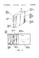
- FIG. 5shows a diagram of a shelve in a cabinet for the optical interface device, which contains a typical set of functional modules in accordance with one embodiment of the present invention.
- FIG. 6is a sequencing flowchart of optical carrier and transmission management decisions carried out by the intelligent optical device in accordance with one embodiment of the present invention.
- FIG. 7is a block diagram of the intelligent optical device incorporating a uni/bidirectional converter in accordance with another embodiment of the present invention.
- Fiber links 202 and 204carry optical data to and from node 101, for example, of FIG. 1 to interconnect equipment 111 and 112 as previously stated.
- a two stage tapped optical amplifier 206boosts the signal for further processing by the signal processing functions as explained below.
- Input stage 1, designated as 210amplifies the optical signal which is then processed by optical interface device 208.
- output stage 2, designated as 212the signal is again strengthened (amplified) by output stage 2, designated as 212, for subsequent transmission through link 204 to another node within the telecommunications network.
- FIG. 2Bshows several exemplary processing functions performed by optical interface device 208 located between the two stages 210 and 212 of the tapped amplifier.
- typical processing of the information carrying optical signalmay include optical carrier management and transmission management.
- Carrier managementcomprises such exemplary functions as wavelength drop/add, wavelength routing, wavelength translation, uni/bi-directional control, etc.
- Some representative operations of the transmission managementare noise filtering, dispersion compensation, additional amplification, regeneration, gain/power equalization, etc. Both carrier and transmission management operations in accordance with the present invention will be explained more fully below.
- the inventive deviceincludes optical amplifier 206 with a tap provided between the two gain stages: input gain stage 210 and output gain stage 212.
- the optical gain stages 210, 212may be implemented using doped fiber amplifiers or semiconductor amplifiers which are commercially available and known to skilled artisans.
- the tapallows for insertion of various processing operations, such as function f1 designated as 302 and functions f2-f7, to be performed upon the information carrying optical signal.
- the first gain stage 210boosts the optical signal at the input of the amplifier: after propagating through a link leading to the node, the signal loses its energy and decreases in amplitude. Consequently, to preserve an operational signal-to-noise ratio, the signal is amplified prior to entering the optical functions f1-f7 which may further decrease the signal strength.
- the second gain stage 212restores the optical signal to a functional transmit power level after the optical processing operations have been performed upon the signal by functions f1-f7.
- optical switch backplane 308A variety of possible optical functions f1-f7 are depicted in FIG. 3. Most of these functions typically have a single input 304 and single output 306, while wavelength multiplexors are a notable exception.
- the inputs and outputs 304, 306 from each functionare connected to optical switch backplane 308 via optical connectors 310.
- optical modulesfor processing information carrying optical signal:
- Amplifieramplifies optical signal using doped fiber or semiconductor amplification.
- Wavelength reference generatorgenerates a stable optical output signal at a specific reference wavelength.
- Dispersion compensatorcounteracts the aberrational effects of a long fiber (i.e. velocity and polarization mode dispersion).
- ASE filterremoves noise caused by amplification of spontaneous emission.
- Wavelength translatorshifts a wavelength of an optical signal.
- Unidirectional/Bidirectional Converterextracts and blends counter-propagating optical signals.
- Wavelength separator/combinerprovides optical grating, or the like, for wavelength division multiplexing and/or demultiplexing.
- Modulation reshaperclarifies the modulation waveform and restores risetime/falltime/duration of the signal.
- Add/drop portsprovide a simple tap to allow a drop/insert of optical signals and may even branch for network build-out.
- Amplitude equalizeradjusts the relative amplitude of several optical wavelengths due to uneven response of optical amplifiers.
- Sub-carrier discriminatorextracts low-level, low-frequency sub-carrier superimposed on the optical signal.
- optical switch backplane 308can connect an output of any function to the input of any another function attached to the backplane.
- FIGS. 4A-4Cshow one exemplary embodiment of optical switch backplane 308 implementing this flexible optical interconnectivity among the functions.
- FIG. 4Ashows the most basic unit, i.e., the building block, of an optical switch: a one-by-two switch 402 which has one input port 403 and a choice of two output ports 404, 406.
- This basic unit of the optical switchmay employ an amplitude beam splitter, or any other technology as known to people skilled in the art.
- one-by-four switching unit 408With one input port and four output ports which you can choose from, three basic one-by-two units 402 are arranged as shown in FIG. 4B.
- one-by-four switching unit 408incudes switch 402 at its input, and at each of the output ports of switch 402 another one-by-two switch 402', 402" is located to supply a choice of four output ports for the optical signal. So, if output port 404' of one-by-four switching unit 408 is desired, the optical signal enters--via input port 403'--one-by-two switch 402 which selects output port 404". The signal via output port 404" serves as input to one-by-two switch 402', which then selects output port 404'.
- FIG. 4Cshows an exemplary four-by-four switch 410 with a choice of four input ports and four output ports. Eight one-by-four switches are employed: four on the input side and four on the output side. Each one-by-four switch comprises three one-by-two switches as shown in FIG. 4B and described above.
- an optical shuffle networkis performed: each output port of the one-by-four switch at the input side is connected to an input port of each one-by-four switch at the output side.
- any inputcan be switched to any of the four outputs.
- an eight-by-eight switch, a sixteen-by-sixteen switch, etc.may be constructed by cascading multiple basic one-by-two switching units.
- the signal from output port 318 of amplifier first stage 210may go to input port 320 of a four-by-four switch of FIG. 4C in optical switch backplane 308.
- the optical signalcan then be switched to any of the output ports 322 of optical switch backplane 308 routing the signal to any of the functions f1-f7 for the appropriate processing.
- the processed signal from a functionis returned to optical switch backplane 308 and may then be reconnected to an input port of the four-by-four switch, for example, for further routing to another output port and processing by another function.
- optical switch backplane 308can determine not only which functions are inserted in the optical path of the information carrying optical signal, but also in which order, i.e., how the signal is processed.
- controller 312which controls the switching action within optical switch backplane 308.
- Controller 312is an electrical device and adds the intelligence and flexibility to the processing operations performed upon the optical signal by functions f1-f7.
- Optical switch backplane 308may be controlled by a remote centralized network control center 314 via an electrical cable or RF signal conduit.
- center 314sends commands to controller 312 which then enables a redundant module or activates another module to re-route the signal within the network.
- modulated signals along the incoming optical carriersmay convey commands to controller 312. This information can then contribute to a decision-making process by controller 312.
- Controller 312may not only receive commands to execute certain functions at the optical switching backplane, but may also notify a supervisory controller of changes in status or configuration. In addition, controller 312 may respond to queries regarding the present capabilities or module content of the optical unit.
- FIG. 3also shows a non-volatile storage device 316 attached to controller 312.
- Non-volatile storage device 316holds the routing logic for controller 312 so that the configuration of optical switch backplane 308 can be quickly restored after a power failure, for example.
- a representative module 302is shaped as a rectangular, solid box containing handle 510 for transporting the module, as well as status indicator lights 514 and power-on indicator 512 on the front portion of the module.
- Lights 514indicate the status of the module, i.e., whether it is currently in operation, etc.
- power-on indicator 512gives a visual indication whether the power is supplied to the module and whether the module is turned on.
- the rear portion of the modulehas optical connectors 310 for attaching to corresponding optical connectors on module shelf 506.
- Coaxial electrical connectors 502are optionally provided on module 302 so that electrical signals may be used for communication within the network in place of optical signals, if desired.
- This multi-wire connectorprovides an electrical communications path between a corresponding module and controller 312: a microprocessor on controller 312 executes computer instructions either embedded in an internal on-chip microprocessor memory or external memory.
- the microprocessorcontrols the operation of the modules f1-f7 in optical switch backplane 308 by establishing communication via a predetermined protocol with a microprocessor in each individual module. Electrical signal are passed between the microprocessors along a multi-wire conduit (bus) into which each module plugs in using connector 504.
- the modulesfit into the shared shelf 506 in an equipment rack by plugging into optical switch backplane 308.
- the moduleshave both electrical and optical connectors which plug into mating connectors in the back of the shelf.
- a representative empty slot 516illustrates corresponding mating connectors for each module in shelf 506 which also contains power supply 508 and tapped amplifier 206. Both power supply 508 and amplifier 206 are designed and constructed as plug-in modules, which are similar to the function modules f1-f7.
- optical switch backplane 308provides flexibility which is currently enjoyed only by electrical-domain networks. A great deal of reconfigurability is possible to accommodate various optical signals or to allow remote changes of optical network configuration on the fly.
- redundant modulesmay be inserted into the optical unit.
- the optical switch backplanecan then perform the fail-over switching. That is, the re-routing of signals is automatically accomplished in the event of partial network failure.
- step 602the optical signal enters the initial amplification stage 210 of amplifier 206.
- step 604the optical carrier requires management or transmission functions. If so, another decision in step 606 is undertaken to determine if the optical carrier must be dropped or re-routed. If, however, no processing operations are to be performed, then in step 624 the carrier is gain and power equalized and directed to the second stage 212 of amplifier 206 in step 626 for subsequent transmission via link 204.
- step 608if carrier is not dropped or re-routed, new optical carriers are added. Whether all optical regeneration is required is determined in step 609. If yes, all optical regeneration of the carrier is performed by the appropriate functional module in step 610, and if no, then another decision is made whether dispersion management is needed in step 612. If so, the dispersion compensator is activated to counteract the aberrational effects of a fiber in step 614.
- step 616a determination is made whether ASE filtering is required and if so, the filtering function is activated to remove noise from the signal. A decision is then carried out in step 620 concerning the wavelength translation. If directed by the logic, the signal wavelength translation function is actuated in step 622, and the optical signal is further processed in steps 624 and 626 as previously described.
- step 606it is determined that the carrier must be either dropped or re-routed, a decision is carried out in step 630 whether to perform a wavelength translation. If so, the signal wavelength translation function is activated in step 632. Otherwise, the carrier is switched to external port, and the processing is terminated in step 636.
- Decision steps 604, 606, 609, 612, 616, 620 and 630require some knowledge about the particular needs of the input optical signal.
- the decisionsmay be affected or influenced by a) input from a supervisory network management system, b) data carried along the incoming optical signal or a sub-carrier thereupon, or c) self-contained detection of the condition of the incoming optical signal.
- FIG. 7Another embodiment of the present invention is shown in FIG. 7, where the elements depicted in this figure correspond to the like-referenced elements in FIG. 3.
- the operation of optical interface device 700 in this embodimentis substantially similar to the embodiment of FIG. 3, except that Bidirectional/Unidirectional Converter 702 is provided in addition to other elements previously described in connection with FIG. 3. While Converter 702 may be external to the optical interface device, it may also exist as another functional module that plugs into the shelf cabinet.
- Unidirectional/Bidirectional Converter 702is connected between the first stage 210 and second stage 212 of amplifier 206 and between links 202 and 204, as shown in FIG. 7.
- Converter 702extracts and blends counter-propagating optical signals such that a two-way path is established along links 202, 204.
- the present inventionfills the need for an agile, all-optical regenerative device to be inserted along a fiber link.
- the flexibility and intelligent control aspects of the present inventionare essential to deployment of an all optical network.
- the present inventionis especially useful in the non-homogeneous environment that will remain in this field throughout the foreseeable future.
Landscapes
- Engineering & Computer Science (AREA)
- Computer Networks & Wireless Communication (AREA)
- Physics & Mathematics (AREA)
- Electromagnetism (AREA)
- Signal Processing (AREA)
- Optical Communication System (AREA)
- Use Of Switch Circuits For Exchanges And Methods Of Control Of Multiplex Exchanges (AREA)
Abstract
Description
Claims (11)
Priority Applications (1)
| Application Number | Priority Date | Filing Date | Title |
|---|---|---|---|
| US08/720,477US5726788A (en) | 1996-09-30 | 1996-09-30 | Dynamically reconfigurable optical interface device using an optically switched backplane |
Applications Claiming Priority (1)
| Application Number | Priority Date | Filing Date | Title |
|---|---|---|---|
| US08/720,477US5726788A (en) | 1996-09-30 | 1996-09-30 | Dynamically reconfigurable optical interface device using an optically switched backplane |
Publications (1)
| Publication Number | Publication Date |
|---|---|
| US5726788Atrue US5726788A (en) | 1998-03-10 |
Family
ID=24894147
Family Applications (1)
| Application Number | Title | Priority Date | Filing Date |
|---|---|---|---|
| US08/720,477Expired - LifetimeUS5726788A (en) | 1996-09-30 | 1996-09-30 | Dynamically reconfigurable optical interface device using an optically switched backplane |
Country Status (1)
| Country | Link |
|---|---|
| US (1) | US5726788A (en) |
Cited By (47)
| Publication number | Priority date | Publication date | Assignee | Title |
|---|---|---|---|---|
| WO2000041370A1 (en)* | 1998-12-30 | 2000-07-13 | Qwest Communications International Inc. | Vdsl cabinet designs and configurations |
| US6092123A (en)* | 1997-07-17 | 2000-07-18 | International Business Machines Corporation | Method and apparatus for changing functions of a hardware device using two or more communication channels |
| US6278689B1 (en) | 1998-04-22 | 2001-08-21 | At&T Corp. | Optical cross-connect restoration technique |
| FR2806558A1 (en)* | 2000-03-15 | 2001-09-21 | Nortel Networks Ltd | Photonic switch for dense wavelength division multiplexed (DWDM) network; directs wavelength from associated egress area along set output path, and combining it into output multi-channel signal transmitted on port |
| WO2001076022A3 (en)* | 2000-04-03 | 2002-03-07 | Corona Optical Systems Inc | Optical amplifier |
| WO2002018999A1 (en)* | 2000-08-25 | 2002-03-07 | Neptec Optical Solutions, Inc. | Network healing smart fiber optic switch |
| US6417964B1 (en)* | 2001-02-05 | 2002-07-09 | Avamex Corporation | Reconfigurable automatic gain control and method for optical amplifier |
| US6421167B1 (en) | 2000-03-03 | 2002-07-16 | General Dynamics Advanced Technology Systems, Inc. | Multiple function bandwidth management systems |
| WO2002057829A1 (en) | 2001-01-17 | 2002-07-25 | The Whitaker Corporation | Optical cross connect |
| US20020131153A1 (en)* | 2001-03-16 | 2002-09-19 | Doshi Bharat Tarachand | Methods and devices for providing optical, serviced-enabled cross-connections |
| US6457978B1 (en)* | 2000-10-10 | 2002-10-01 | Cadent, Inc. | Method and apparatus for arranging cable connectors to allow for easier cable installation |
| US6493119B1 (en)* | 1999-09-07 | 2002-12-10 | Chien-Yu Kuo | Scalable DWDM network switch architecture with wavelength tunable sources |
| US20030058497A1 (en)* | 2001-09-27 | 2003-03-27 | Nortel Networks Limited | All-optical switching sites for an agile optical network |
| US20030091274A1 (en)* | 2001-11-05 | 2003-05-15 | Vohra Sandeep J. | Configurable optical add/drop multiplexer with partial or complete wavelength drop capability |
| EP1161008A3 (en)* | 2000-05-31 | 2003-05-21 | Agere Systems Optoelectronics Guardian Corporation | High power, multiple-tap co-doped optical amplifier |
| US20030108270A1 (en)* | 2001-12-05 | 2003-06-12 | Brimacombe Robert K. | Visible light tracer for high power-carrying optical fibers |
| US6587240B1 (en)* | 1998-12-21 | 2003-07-01 | Agilent Technologies, Inc. | Optical switching node and method for operating same |
| US20030152305A1 (en)* | 2002-02-11 | 2003-08-14 | Mcglashan-Powell Maurice | Magneto-optical switching backplane for processor interconnection |
| WO2003075165A1 (en)* | 2002-02-28 | 2003-09-12 | Novilit, Inc. | Optical communication apparatus and method |
| US6650808B1 (en)* | 1999-10-14 | 2003-11-18 | Raytheon Company | Optical high speed bus for a modular computer network |
| US6661940B2 (en) | 2000-07-21 | 2003-12-09 | Finisar Corporation | Apparatus and method for rebroadcasting signals in an optical backplane bus system |
| US20040100684A1 (en)* | 2001-06-07 | 2004-05-27 | Jones Kevan Peter | Line amplification system for wavelength switched optical networks |
| FR2849729A1 (en)* | 2003-06-12 | 2004-07-09 | France Telecom | Optical fiber cross connecting arrangement for use in communication network, has control unit associated with diagnostic unit to answer particular diagnostic to automatically control adapted commutation of distributor |
| US20040228627A1 (en)* | 2003-05-15 | 2004-11-18 | International Business Machines Corporation | Highly available redundant optical modules using single network connection |
| US20040264843A1 (en)* | 2002-03-18 | 2004-12-30 | Tomasz Leonczuk | Optically powered optically controlled optical switch |
| US6839163B1 (en)* | 1999-09-01 | 2005-01-04 | Avanex Corporation | Apparatus and method for making an optical fiber amplifier |
| US6839164B2 (en)* | 2000-03-29 | 2005-01-04 | Hitachi, Ltd. | Optical transmission equipment and supervisory system thereof |
| US6848841B2 (en) | 2002-09-09 | 2005-02-01 | Hewlett-Packard Development Company, L.P. | Optical component connector |
| US20050074236A1 (en)* | 2003-10-07 | 2005-04-07 | Neptec Optical Solutions, Inc. | Optical network monitoring system |
| US6907159B1 (en) | 2002-02-21 | 2005-06-14 | Broadband Royalty Corporation | Configurable optical add/drop multiplexer with enhanced add channel capacity |
| US6912337B2 (en) | 2000-08-25 | 2005-06-28 | Neptec Optical Solutions, Inc. | Network healing smart fiber optic switch |
| US20060153493A1 (en)* | 2005-01-12 | 2006-07-13 | Neptec Optical Solutions, Inc. | Optical switch array for routing multiple optical signals |
| US20060153494A1 (en)* | 2005-01-12 | 2006-07-13 | Neptec Optical Solutions, Inc. | Optical switch for routing multiple optical signals |
| US20060251416A1 (en)* | 2005-05-06 | 2006-11-09 | Lockheed Martin Corporation | Switching module |
| US20060253744A1 (en)* | 2005-02-14 | 2006-11-09 | Mayes Joseph E | Fibre selective control switch system |
| FR2894036A1 (en)* | 2005-11-30 | 2007-06-01 | Alcatel Sa | Optical switching device for transparent switching node e.g. transparent optical cross connect, has fusion and additional fusion modules each comprising inputs coupled to respective outputs of broadcasting modules |
| US20070274721A1 (en)* | 2001-05-07 | 2007-11-29 | Charles Barker | N-way broadcast / narrowcast combiner |
| KR100798979B1 (en)* | 2000-12-10 | 2008-01-28 | 이씨아이 텔레콤 리미티드 | Modules and Methods for Rebuilding Optical Networks |
| US20080068701A1 (en)* | 2004-10-29 | 2008-03-20 | Wysocki Paul F | Article Comprising a Multichannel Optical Amplified Transmission System with Functional Upgrade Capabilities and Universal Modules |
| US7356213B1 (en)* | 2006-03-28 | 2008-04-08 | Sun Microsystems, Inc. | Transparent switch using optical and electrical proximity communication |
| US20080219666A1 (en)* | 1998-12-14 | 2008-09-11 | Tellabs Operations, Inc. | Optical line terminal arrangement, apparatus and methods |
| US20090175625A1 (en)* | 2002-06-26 | 2009-07-09 | Giuseppe Morfino | Optically connected system for exchanging data among industrial automation devices |
| US20090226138A1 (en)* | 2005-11-28 | 2009-09-10 | Amphotonix Limited | Fibre-Optic Module |
| US20110235285A1 (en)* | 2010-03-23 | 2011-09-29 | Thomas Cloonan | Interface port configuration to reduce connection interference |
| US20130121701A1 (en)* | 2002-06-26 | 2013-05-16 | Fidia S.P.A. | Optically-connected system for exchanging data among industrial automation devices |
| US20140040524A1 (en)* | 2011-03-30 | 2014-02-06 | Fujitsu Technology Solutions Intellectual Property Gmbh | Rack, server and assembly comprising such a rack and at least one server |
| US8854980B2 (en) | 2005-05-06 | 2014-10-07 | Lockheed Martin Corporation | Switching module |
- 1996
- 1996-09-30USUS08/720,477patent/US5726788A/ennot_activeExpired - Lifetime
Non-Patent Citations (4)
| Title |
|---|
| Robinson et al., "Performance of an optical backplane bus for switch interconnection", IEE Proc.-Optoelectron., vol. 143, No. 4, Aug. 1996. |
| Robinson et al., "The Optical Backplane Bus As The Interconnection Network of A Switch", IEE, 1995. |
| Robinson et al., Performance of an optical backplane bus for switch interconnection , IEE Proc. Optoelectron., vol. 143, No. 4, Aug. 1996.* |
| Robinson et al., The Optical Backplane Bus As The Interconnection Network of A Switch , IEE, 1995.* |
Cited By (74)
| Publication number | Priority date | Publication date | Assignee | Title |
|---|---|---|---|---|
| US6092123A (en)* | 1997-07-17 | 2000-07-18 | International Business Machines Corporation | Method and apparatus for changing functions of a hardware device using two or more communication channels |
| US6278689B1 (en) | 1998-04-22 | 2001-08-21 | At&T Corp. | Optical cross-connect restoration technique |
| US9014562B2 (en) | 1998-12-14 | 2015-04-21 | Coriant Operations, Inc. | Optical line terminal arrangement, apparatus and methods |
| US20080219666A1 (en)* | 1998-12-14 | 2008-09-11 | Tellabs Operations, Inc. | Optical line terminal arrangement, apparatus and methods |
| US6587240B1 (en)* | 1998-12-21 | 2003-07-01 | Agilent Technologies, Inc. | Optical switching node and method for operating same |
| US6219354B1 (en)* | 1998-12-30 | 2001-04-17 | Qwest Communications International Inc. | VDSL cabinet designs and configurations |
| WO2000041370A1 (en)* | 1998-12-30 | 2000-07-13 | Qwest Communications International Inc. | Vdsl cabinet designs and configurations |
| US6839163B1 (en)* | 1999-09-01 | 2005-01-04 | Avanex Corporation | Apparatus and method for making an optical fiber amplifier |
| US6493119B1 (en)* | 1999-09-07 | 2002-12-10 | Chien-Yu Kuo | Scalable DWDM network switch architecture with wavelength tunable sources |
| US6650808B1 (en)* | 1999-10-14 | 2003-11-18 | Raytheon Company | Optical high speed bus for a modular computer network |
| EP1111953A3 (en)* | 1999-12-22 | 2004-09-15 | Agilent Technologies, Inc. (a Delaware corporation) | An optical switching node and method for operating same |
| US6421167B1 (en) | 2000-03-03 | 2002-07-16 | General Dynamics Advanced Technology Systems, Inc. | Multiple function bandwidth management systems |
| FR2806558A1 (en)* | 2000-03-15 | 2001-09-21 | Nortel Networks Ltd | Photonic switch for dense wavelength division multiplexed (DWDM) network; directs wavelength from associated egress area along set output path, and combining it into output multi-channel signal transmitted on port |
| US6839164B2 (en)* | 2000-03-29 | 2005-01-04 | Hitachi, Ltd. | Optical transmission equipment and supervisory system thereof |
| WO2001076022A3 (en)* | 2000-04-03 | 2002-03-07 | Corona Optical Systems Inc | Optical amplifier |
| EP1161008A3 (en)* | 2000-05-31 | 2003-05-21 | Agere Systems Optoelectronics Guardian Corporation | High power, multiple-tap co-doped optical amplifier |
| US6661940B2 (en) | 2000-07-21 | 2003-12-09 | Finisar Corporation | Apparatus and method for rebroadcasting signals in an optical backplane bus system |
| US6430335B1 (en)* | 2000-08-25 | 2002-08-06 | Neptec Optical Solutions, Inc. | Network healing smart fiber optic switch |
| US6912337B2 (en) | 2000-08-25 | 2005-06-28 | Neptec Optical Solutions, Inc. | Network healing smart fiber optic switch |
| WO2002018999A1 (en)* | 2000-08-25 | 2002-03-07 | Neptec Optical Solutions, Inc. | Network healing smart fiber optic switch |
| US6457978B1 (en)* | 2000-10-10 | 2002-10-01 | Cadent, Inc. | Method and apparatus for arranging cable connectors to allow for easier cable installation |
| KR100798979B1 (en)* | 2000-12-10 | 2008-01-28 | 이씨아이 텔레콤 리미티드 | Modules and Methods for Rebuilding Optical Networks |
| EP1370894A4 (en)* | 2001-01-17 | 2007-04-04 | Whitaker Corp | OPTICAL CROSSCONNECT |
| WO2002057829A1 (en) | 2001-01-17 | 2002-07-25 | The Whitaker Corporation | Optical cross connect |
| US6417964B1 (en)* | 2001-02-05 | 2002-07-09 | Avamex Corporation | Reconfigurable automatic gain control and method for optical amplifier |
| US20020131153A1 (en)* | 2001-03-16 | 2002-09-19 | Doshi Bharat Tarachand | Methods and devices for providing optical, serviced-enabled cross-connections |
| US7620273B2 (en)* | 2001-03-16 | 2009-11-17 | Alcatel-Lucent Usa Inc. | Methods and devices for providing optical, serviced-enabled cross-connections |
| US8111991B2 (en) | 2001-05-07 | 2012-02-07 | Aurora Networks Inc. | N-way broadcast / narrowcast combiner |
| US20070274721A1 (en)* | 2001-05-07 | 2007-11-29 | Charles Barker | N-way broadcast / narrowcast combiner |
| US20040100684A1 (en)* | 2001-06-07 | 2004-05-27 | Jones Kevan Peter | Line amplification system for wavelength switched optical networks |
| US20030058497A1 (en)* | 2001-09-27 | 2003-03-27 | Nortel Networks Limited | All-optical switching sites for an agile optical network |
| WO2003028403A3 (en)* | 2001-09-27 | 2003-09-18 | Nortel Networks Ltd | All-optical switching sites for an agile optical network |
| WO2003041320A3 (en)* | 2001-11-05 | 2004-02-12 | Optinel Systems Inc | Configurable optical add/drop multiplexer with partial or complete wavelength drop capability |
| US20030091274A1 (en)* | 2001-11-05 | 2003-05-15 | Vohra Sandeep J. | Configurable optical add/drop multiplexer with partial or complete wavelength drop capability |
| US6907158B2 (en) | 2001-11-05 | 2005-06-14 | Broadband Royalty Corporation | Configurable optical add/drop multiplexer with partial or complete wavelength drop capability |
| US20030108270A1 (en)* | 2001-12-05 | 2003-06-12 | Brimacombe Robert K. | Visible light tracer for high power-carrying optical fibers |
| US6816637B2 (en)* | 2002-02-11 | 2004-11-09 | International Business Machines Corporation | Magneto-optical switching backplane for processor interconnection |
| US20040208472A1 (en)* | 2002-02-11 | 2004-10-21 | International Business Machines Corporation | Magneto-optical switching backplane for processor interconnection |
| US20030152305A1 (en)* | 2002-02-11 | 2003-08-14 | Mcglashan-Powell Maurice | Magneto-optical switching backplane for processor interconnection |
| US6983097B2 (en)* | 2002-02-11 | 2006-01-03 | International Business Machines Corporation | Magneto-optical switching backplane for processor interconnection |
| US6907159B1 (en) | 2002-02-21 | 2005-06-14 | Broadband Royalty Corporation | Configurable optical add/drop multiplexer with enhanced add channel capacity |
| WO2003075165A1 (en)* | 2002-02-28 | 2003-09-12 | Novilit, Inc. | Optical communication apparatus and method |
| US6987900B2 (en)* | 2002-03-18 | 2006-01-17 | Aurora Networks, Inc. | Optically powered optically controlled optical switch |
| US20040264843A1 (en)* | 2002-03-18 | 2004-12-30 | Tomasz Leonczuk | Optically powered optically controlled optical switch |
| US20090175625A1 (en)* | 2002-06-26 | 2009-07-09 | Giuseppe Morfino | Optically connected system for exchanging data among industrial automation devices |
| US20130121701A1 (en)* | 2002-06-26 | 2013-05-16 | Fidia S.P.A. | Optically-connected system for exchanging data among industrial automation devices |
| US20120269518A1 (en)* | 2002-06-26 | 2012-10-25 | Fidia S.P.A. | Optically-connected system for exchanging data among industrial automation devices |
| US8565611B2 (en)* | 2002-06-26 | 2013-10-22 | Fidia S.P.A. | Optically-connected system for exchanging data among industrial automation devices |
| US6848841B2 (en) | 2002-09-09 | 2005-02-01 | Hewlett-Packard Development Company, L.P. | Optical component connector |
| US20040228627A1 (en)* | 2003-05-15 | 2004-11-18 | International Business Machines Corporation | Highly available redundant optical modules using single network connection |
| US7551850B2 (en)* | 2003-05-15 | 2009-06-23 | International Business Machines Corporation | Highly available redundant optical modules using single network connection |
| FR2849729A1 (en)* | 2003-06-12 | 2004-07-09 | France Telecom | Optical fiber cross connecting arrangement for use in communication network, has control unit associated with diagnostic unit to answer particular diagnostic to automatically control adapted commutation of distributor |
| US20050074236A1 (en)* | 2003-10-07 | 2005-04-07 | Neptec Optical Solutions, Inc. | Optical network monitoring system |
| US7999999B2 (en)* | 2004-10-29 | 2011-08-16 | Unopsys, Llc | Article comprising a multichannel optical amplified transmission system with functional upgrade capabilities and universal modules |
| US20080068701A1 (en)* | 2004-10-29 | 2008-03-20 | Wysocki Paul F | Article Comprising a Multichannel Optical Amplified Transmission System with Functional Upgrade Capabilities and Universal Modules |
| US20060153494A1 (en)* | 2005-01-12 | 2006-07-13 | Neptec Optical Solutions, Inc. | Optical switch for routing multiple optical signals |
| US7184618B2 (en) | 2005-01-12 | 2007-02-27 | Neptec Optical Solutions, Inc. | Optical switch array for routing multiple optical signals |
| US20060153493A1 (en)* | 2005-01-12 | 2006-07-13 | Neptec Optical Solutions, Inc. | Optical switch array for routing multiple optical signals |
| US7620320B2 (en)* | 2005-02-14 | 2009-11-17 | Lsi Corporation | Fibre selective control switch system |
| US20060253744A1 (en)* | 2005-02-14 | 2006-11-09 | Mayes Joseph E | Fibre selective control switch system |
| US20060251416A1 (en)* | 2005-05-06 | 2006-11-09 | Lockheed Martin Corporation | Switching module |
| US8854980B2 (en) | 2005-05-06 | 2014-10-07 | Lockheed Martin Corporation | Switching module |
| US9253030B2 (en) | 2005-05-06 | 2016-02-02 | Lockheed Martin Corporation | Switching module |
| US9515903B2 (en) | 2005-05-06 | 2016-12-06 | Lockheed Martin Corporation | Switching module |
| US20090226138A1 (en)* | 2005-11-28 | 2009-09-10 | Amphotonix Limited | Fibre-Optic Module |
| CN1984502B (en)* | 2005-11-30 | 2010-12-22 | 阿尔卡特公司 | Optical switching device for a transparent node of high switching degree adapted to spectral equalization |
| US7653307B2 (en) | 2005-11-30 | 2010-01-26 | Alcatel Lucent | Optical switching device for a transparent node of high switching degree adapted to spectral equalization |
| US20070183777A1 (en)* | 2005-11-30 | 2007-08-09 | Alcatel | Optical switching device for a transparent node of high switching degree adapted to spectral equalization |
| EP1793644A1 (en)* | 2005-11-30 | 2007-06-06 | Alcatel Lucent | Optical communication device for a transparent node with spectral equalisation capability |
| FR2894036A1 (en)* | 2005-11-30 | 2007-06-01 | Alcatel Sa | Optical switching device for transparent switching node e.g. transparent optical cross connect, has fusion and additional fusion modules each comprising inputs coupled to respective outputs of broadcasting modules |
| US7356213B1 (en)* | 2006-03-28 | 2008-04-08 | Sun Microsystems, Inc. | Transparent switch using optical and electrical proximity communication |
| US20110235285A1 (en)* | 2010-03-23 | 2011-09-29 | Thomas Cloonan | Interface port configuration to reduce connection interference |
| US20140040524A1 (en)* | 2011-03-30 | 2014-02-06 | Fujitsu Technology Solutions Intellectual Property Gmbh | Rack, server and assembly comprising such a rack and at least one server |
| US9582450B2 (en)* | 2011-03-30 | 2017-02-28 | Fujitsu Technology Solutions Intellectual Property Gmbh | Rack, server and assembly comprising such a rack and at least one server |
Similar Documents
| Publication | Publication Date | Title |
|---|---|---|
| US5726788A (en) | Dynamically reconfigurable optical interface device using an optically switched backplane | |
| US8554074B2 (en) | Colorless, directionless, and gridless optical network, node, and method | |
| US5986783A (en) | Method and apparatus for operation, protection, and restoration of heterogeneous optical communication networks | |
| US6272154B1 (en) | Reconfigurable multiwavelength network elements | |
| US6046833A (en) | Method and apparatus for operation, protection, and restoration of heterogeneous optical communication networks | |
| US20020186432A1 (en) | Architecture for a photonic transport network | |
| EP1183801B1 (en) | A highly scalable modular optical amplifier based subsystem | |
| US8131149B2 (en) | Optical routing device and optical network using same | |
| US7206508B2 (en) | Method and apparatus for operation, protection, and restoration of heterogeneous optical communication networks | |
| WO1998047039A9 (en) | Method and apparatus for operation, protection, and restoration of heterogeneous optical communication networks | |
| US9014562B2 (en) | Optical line terminal arrangement, apparatus and methods | |
| CA2393633A1 (en) | Method for engineering connections in a dynamically reconfigurable photonic switched network | |
| US20010040710A1 (en) | Optical communication system | |
| JP2008271603A (en) | Optical network and protection switching method | |
| US9742520B1 (en) | Optical switching system with a colorless, directionless, and contentionless ROADM connected to unamplified drop channels | |
| EP3923489B1 (en) | Optical switching and electrical powering architecture for undersea mesh networking | |
| JP2006191643A (en) | Optical network, hub node and access node | |
| US5930017A (en) | Method and system for maintaining an optical path | |
| EP1014613A2 (en) | Shared optical protection in an optical communications network | |
| US20050196169A1 (en) | System and method for communicating traffic between optical rings | |
| US20040228631A1 (en) | Optical communication system and method for using same | |
| US20150256282A1 (en) | Symmetric optical multiplexing node | |
| US6317230B1 (en) | Optical cross-connect system and optical transmission system | |
| US6504631B1 (en) | System and method providing control channel for wavelength-division multiplexed network | |
| WO1999045719A1 (en) | Optical shuffle network interconnection |
Legal Events
| Date | Code | Title | Description |
|---|---|---|---|
| AS | Assignment | Owner name:MCI COMMUNICATIONS CORPORATION, DISTRICT OF COLUMB Free format text:ASSIGNMENT OF ASSIGNORS INTEREST;ASSIGNORS:FEE, JOHN;LIU, SHOA-KAI;ROBINSON, NIALL;AND OTHERS;REEL/FRAME:008227/0425 Effective date:19960913 | |
| STCF | Information on status: patent grant | Free format text:PATENTED CASE | |
| FPAY | Fee payment | Year of fee payment:4 | |
| FPAY | Fee payment | Year of fee payment:8 | |
| FPAY | Fee payment | Year of fee payment:12 | |
| FEPP | Fee payment procedure | Free format text:PAYER NUMBER DE-ASSIGNED (ORIGINAL EVENT CODE: RMPN); ENTITY STATUS OF PATENT OWNER: LARGE ENTITY | |
| AS | Assignment | Owner name:VERIZON PATENT AND LICENSING INC., NEW JERSEY Free format text:ASSIGNMENT OF ASSIGNORS INTEREST;ASSIGNOR:MCI COMMUNICATIONS CORPORATION;REEL/FRAME:028833/0449 Effective date:20120821 | |
| AS | Assignment | Owner name:IRINEI SOLUTIONS, L.L.C., DELAWARE Free format text:ASSIGNMENT OF ASSIGNORS INTEREST;ASSIGNOR:VERIZON PATENT AND LICENSING INC.;REEL/FRAME:029147/0242 Effective date:20120918 | |
| AS | Assignment | Owner name:MCI COMMUNICATIONS CORPORATION, DISTRICT OF COLUMB Free format text:CORRECTIVE ASSIGNMENT TO CORRECT THE FIRST AND THIRD ASSIGNOR'S NAMES AND EXECUTION DATES FOR SHOA-KAI LIU, ANDREW NIALL ROBINSON AND REDDY URIMINDI PREVIOUSLY RECORDED ON REEL 008227 FRAME 0425. ASSIGNOR(S) HEREBY CONFIRMS THE NAME OF ASSIGNORS AS JOHN A. FEE AND ANDREW NIALL ROBINSON AND THE EXECUTION DATE AS 9/11/1996 FOR THE LAST THREE ASSIGNORS;ASSIGNORS:FEE, JOHN A.;LIU, SHOA-KAI;ROBINSON, ANDREW NIALL;AND OTHERS;SIGNING DATES FROM 19960911 TO 19960913;REEL/FRAME:029700/0903 | |
| AS | Assignment | Owner name:VERIZON PATENT AND LICENSING INC., NEW JERSEY Free format text:ASSIGNMENT OF ASSIGNORS INTEREST;ASSIGNOR:MCI COMMUNICATIONS CORPORATION;REEL/FRAME:032725/0001 Effective date:20140409 | |
| AS | Assignment | Owner name:VERIZON PATENT AND LICENSING INC., NEW JERSEY Free format text:CORRECTIVE ASSIGNMENT TO REMOVE THE PATENT NUMBER 5,835,907 PREVIOUSLY RECORDED ON REEL 032725 FRAME 0001. ASSIGNOR(S) HEREBY CONFIRMS THE ASSIGNMENT;ASSIGNOR:MCI COMMUNICATIONS CORPORATION;REEL/FRAME:033408/0235 Effective date:20140409 | |
| AS | Assignment | Owner name:TAMIRAS PER PTE. LTD., LLC, DELAWARE Free format text:MERGER;ASSIGNOR:IRINEI SOLUTIONS, L.L.C.;REEL/FRAME:037260/0221 Effective date:20150903 |