US5726440A - Wavelength selective photodetector - Google Patents
Wavelength selective photodetectorDownload PDFInfo
- Publication number
- US5726440A US5726440AUS08/553,875US55387595AUS5726440AUS 5726440 AUS5726440 AUS 5726440AUS 55387595 AUS55387595 AUS 55387595AUS 5726440 AUS5726440 AUS 5726440A
- Authority
- US
- United States
- Prior art keywords
- wavelength selective
- photodetector according
- selective photodetector
- layer
- upper section
- Prior art date
- Legal status (The legal status is an assumption and is not a legal conclusion. Google has not performed a legal analysis and makes no representation as to the accuracy of the status listed.)
- Expired - Fee Related
Links
Images


Classifications
- H—ELECTRICITY
- H10—SEMICONDUCTOR DEVICES; ELECTRIC SOLID-STATE DEVICES NOT OTHERWISE PROVIDED FOR
- H10F—INORGANIC SEMICONDUCTOR DEVICES SENSITIVE TO INFRARED RADIATION, LIGHT, ELECTROMAGNETIC RADIATION OF SHORTER WAVELENGTH OR CORPUSCULAR RADIATION
- H10F30/00—Individual radiation-sensitive semiconductor devices in which radiation controls the flow of current through the devices, e.g. photodetectors
- H10F30/20—Individual radiation-sensitive semiconductor devices in which radiation controls the flow of current through the devices, e.g. photodetectors the devices having potential barriers, e.g. phototransistors
- H10F30/21—Individual radiation-sensitive semiconductor devices in which radiation controls the flow of current through the devices, e.g. photodetectors the devices having potential barriers, e.g. phototransistors the devices being sensitive to infrared, visible or ultraviolet radiation
- H10F30/22—Individual radiation-sensitive semiconductor devices in which radiation controls the flow of current through the devices, e.g. photodetectors the devices having potential barriers, e.g. phototransistors the devices being sensitive to infrared, visible or ultraviolet radiation the devices having only one potential barrier, e.g. photodiodes
- H10F30/221—Individual radiation-sensitive semiconductor devices in which radiation controls the flow of current through the devices, e.g. photodetectors the devices having potential barriers, e.g. phototransistors the devices being sensitive to infrared, visible or ultraviolet radiation the devices having only one potential barrier, e.g. photodiodes the potential barrier being a PN homojunction
- H—ELECTRICITY
- H10—SEMICONDUCTOR DEVICES; ELECTRIC SOLID-STATE DEVICES NOT OTHERWISE PROVIDED FOR
- H10F—INORGANIC SEMICONDUCTOR DEVICES SENSITIVE TO INFRARED RADIATION, LIGHT, ELECTROMAGNETIC RADIATION OF SHORTER WAVELENGTH OR CORPUSCULAR RADIATION
- H10F71/00—Manufacture or treatment of devices covered by this subclass
- H10F71/121—The active layers comprising only Group IV materials
- H10F71/1215—The active layers comprising only Group IV materials comprising at least two Group IV elements, e.g. SiGe
- Y—GENERAL TAGGING OF NEW TECHNOLOGICAL DEVELOPMENTS; GENERAL TAGGING OF CROSS-SECTIONAL TECHNOLOGIES SPANNING OVER SEVERAL SECTIONS OF THE IPC; TECHNICAL SUBJECTS COVERED BY FORMER USPC CROSS-REFERENCE ART COLLECTIONS [XRACs] AND DIGESTS
- Y02—TECHNOLOGIES OR APPLICATIONS FOR MITIGATION OR ADAPTATION AGAINST CLIMATE CHANGE
- Y02E—REDUCTION OF GREENHOUSE GAS [GHG] EMISSIONS, RELATED TO ENERGY GENERATION, TRANSMISSION OR DISTRIBUTION
- Y02E10/00—Energy generation through renewable energy sources
- Y02E10/50—Photovoltaic [PV] energy
Definitions
- the present inventionrelates generally to semiconductor photodetectors. More particularly, the invention relates to monolithic wavelength selective photodetectors which implement wavelength selectivity without use of external optical filters. The invention is especially useful for detection of ultraviolet (UV) emissions.
- UVultraviolet
- UV light detectorsare useful, for example, in hydrogen and hydrocarbon flame detectors, ozone layer thickness monitors and dosimeters for monitoring harmful UV radiation from the sun.
- UV sensitive camerafor observing hydrogen flames at 309 nm.
- That systememploys a quartz and CaF achromatic lens coupled to a UV image intensifier.
- the UV image intensifierfiber-couples to a focus projection scan vidicon.
- Interference filtersselect the emission band to be monitored.
- the filtersare designed to discriminate against background visible and IR radiation.
- this detection systemperforms reasonably well, it suffers from several disadvantages. For example, it is relatively large, complex and expensive to build and maintain. Additionally, as a result of using interference filters, the UV signals being monitored are typically attenuated to about 3%-4% of their original strength.
- an object of the present inventionis to provide a filterless wavelength selective photodetector.
- a further object of the inventionis to provide a compact inexpensive wavelength selective photodetector.
- An additional object of the inventionis to provide a compact inexpensive wavelength selective photodetector that is suitable for monitoring UV emissions.
- Another object of the inventionis to provide a wavelength selective photodetector that is suitable for operation as a flame detector.
- a further object of the inventionis to provide a wavelength selective photodetector that is suitable for monitoring ozone depletion, or build up.
- the photodetectorincludes a substrate, preferably Si based, having a buried insulator layer, and a photodetection element.
- the insulator layeris preferably fabricated at a selected depth in the substrate and electrically isolates a lower section of the substrate located below the insulator from an upper section of the substrate located above the insulator.
- the insulator layercan be constructed from silicon oxide, silicon dioxide, silicon nitride, silicon oxynitride or aluminum oxide.
- the photodetection elementwhich is preferably a photodiode, is fabricated on the upper section of the substrate.
- the selected depth at which the insulator layer is formeddetermines the thickness of the upper section, and contributes to determining the long wavelength cutoff of the photodetector.
- the long wavelength cutoffis also affected by the energy band gap of the material from which the top section is fabricated.
- the upper sectionis fabricated from Si.
- the upper sectionis fabricated from SiC.
- the upper sectionis formed as a dual layer structure having a top layer of SiC and a bottom layer of Si.
- a wavelength selective photodetector according to the inventionhas a broad range of applications.
- the inventioncan be employed in hydrogen flame detectors, ozone layer thickness monitors and UV dosimeters for detecting harmful UV solar emissions.
- the inventionis employed in time-out monitors for aircraft engines, hydrocarbon flame monitors for residential and commercial heating systems and furnaces, safety devices for flammable gas storage facilities, dosimeters for monitoring light during UV curing applications, and various other analytical and clinical instrumentation. Accordingly, it is especially useful to fabricate the invention to be particularly sensitive to UV light, while being insensitive to other wavelengths of light, such as light in the visible and infrared (IR) wavelength ranges.
- IRvisible and infrared
- a photodetectorhas an upper layer that is fabricated from Si and is between about 2000 ⁇ and about 4000 ⁇ thick to detect light in a range between about 300 nm and about 400 nm.
- the upper layerhas a thickness of less than about 2000 ⁇ to provide an even lower long wavelength cutoff and thus, reduced sensitivity to light in the IR and visible wavelength ranges.
- the photodetection elementis a photodiode fabricated on the upper section of the substrate.
- an implantation maskwhich shields the upper layer from incident light, is formed on a portion of the top surface of the upper section.
- the photodiodeis fabricated on a portion of the upper section that is not covered by the implantation mask.
- the maskcan be formed from Si 3 N 4 or SiO 2 , and preferably, has a thickness in a range between about 5000 ⁇ and about 10000 ⁇ .
- the photodiodecan be fabricated from a semiconductor junction between an n-type doped region of the upper section and a p-type doped region of the upper section.
- the n-type doped regionis formed on the p-type doped region.
- the p-type doped regionis formed on the n-type doped region.
- the n-type dopantis preferably arsenic (As) and the p-type dopant is preferably boron (B).
- the p-type doped regioncan be doped to have a dopant concentration in a range between about 1 ⁇ 10 15 cm 3 and about 1 ⁇ 10 18 /cm 3 and the n-type doped region can be doped to have a dopant concentration in a range between about 1 ⁇ 10 17 /cm 3 and about 1 ⁇ 10 20 /cm 3 .
- the n-type doped regioncan be doped to have a dopant concentration in a range between about 1 ⁇ 10 15 /cm 3 and about 1 ⁇ 10 18 /cm 3 and the p-type doped region can be doped to have a dopant concentration in a range between about 1 ⁇ 10 17 /cm 3 and about 1 ⁇ 10 20 /cm 3 .
- the upper region in either the n-on-p or p-on-n structurehas a higher doping concentration than does the lower region.
- the p-type dopantis preferably aluminum (Al) or boron (B) and the n-type dopant is preferably nitrogen (N) or phosphorous (P).
- the upper sectionis fabricated as a two layer structure.
- the top layeris SiC and the bottom layer is Si.
- the photodiodecan be formed either as a homojunction, i.e. completely within the SiC layer, or heterojunction, i.e. with the junction formed at the interface of the SiC layer and the Si layer.
- a photodetectorpreferably includes first and second ohmic contacts for electrically connecting to the photodiode junction for providing access to the electrical output signal.
- the photodetectorincludes an antireflective coating at the surface for reducing reflectance at wavelengths shorter than the long wavelength cutoff.
- the antireflective coatingcan be formed, for example, from one or more layers of, SiO, SiO 2 , ZnS, Si 3 N 4 , TiO 2 , Ta 2 O.sub., SiC and/or MgF.
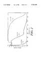
- FIG. 1is a cross sectional view of a wavelength selective photodetector according to one embodiment of the invention
- FIG. 2shows a comparison of quantum efficiency as a function of wavelength between several wavelength selective photodetectors fabricated in accordance with the present invention
- FIG. 3depicts the relationship between the thickness of silicon and the wavelength of light that it absorbs
- FIGS. 4A-4Fdepict abridged processing steps for fabricating a wavelength selective photodetector of the type shown in FIG. 1;
- FIGS. 5A-5Edepict alternative processing steps for fabricating a wavelength selective photodetector of the type shown in FIG. 1;
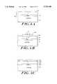
- FIGS. 6A and 6Bshow alternative photodiode junction arrangements for the wavelength selective photodetector of FIG. 1;
- FIG. 7is a cross sectional view of an alternative embodiment of the invention employing SiC in the upper section of the wavelength selective photodetector of FIG. 1;
- FIGS. 8A-8Ddepict abridged processing steps for fabricating a wavelength selective photodetector of the type shown in FIG. 7;
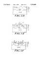
- FIGS. 9A-9Care cross sectional views of an alternative embodiment of the invention employing a dual layer structure in the upper section of the wavelength selective photodetector of FIG. 1;
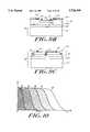
- FIG. 10is a graph representative of the integrated spectral response of an array of wavelength selective photodetectors
- FIG. 11is conceptual schematic of an array of photodetectors according to an alternative embodiment of the invention.
- FIGS. 12A-12Ddepict abridged processing steps for fabricating an array of photodetectors such as that conceptually shown in FIG. 11;
- FIG. 13is a block diagram illustrating the use of a wavelength selective photodetector according to the invention in a multipurpose alarm system.
- FIG. 14is a block diagram illustrating the use of a wavelength selective photodetector according to the invention in a multipurpose dosimetric system.
- the present inventionrelates generally to wavelength selective photodetectors. More particularly, the invention relates to solid-state wavelength selective photodetectors which implement wavelength selectivity without use of external optical filters. According to a preferred embodiment, the present invention employs silicon-on-insulator (SOI) structures to realize filterless, wavelength selective detectors which can efficiently detect photons of particular wavelengths, while exhibiting minimum sensitivity to photons of other wavelengths.
- SOIsilicon-on-insulator
- FIG. 1shows a cross sectional view of a wavelength selective photodetector 100 according to one embodiment of the invention.
- the detector 100includes a buffed insulator layer 102 implanted to a selected depth below the surface 104 of a Si substrate 106.
- the buried insulator layer 102divides the Si substrate 106 into a relatively thin upper section 108 and a relatively thick lower section 110. The depth to which the buried layer is implanted determines the thickness of the upper section 108.
- a photodiode 112is fabricated on the upper section 108.
- the upper section 108is preferably p-type doped.
- the photodiode 112includes an n-type doped layer 114 formed on the p-type doped upper section 108.
- Ohmic contact 116formed as a ring on the n-type doped layer 114, provides electrical connection to that layer
- ohmic contact 120formed as a ring on p-type doped section 108
- An implantation mask 124is formed on the upper section 108.
- an antireflective (AR) coating 126for minimizing reflectance in a selected wavelength range is formed on the photodiode 112.
- photons of lightfall incident on the detector 100, they pass through the n-on-p junction of diode 112. As photons pass through the upper semiconducting layers 114 and 108, they generate electron-hole pairs which are separated at the pn junction. As a result, a current is generated across the junction. That current can be sensed between terminal 116 which contacts layer 114, and terminal 120 which contacts upper section 108. Once the incident photons pass through the photodiode 112, they strike insulator 102. Photons having a wavelength greater than a selected long wavelength cutoff pass through the insulator layer 102 and are dissipated within the lower section 110 of substrate 106.
- Photons having a wavelength less than the selected long wavelength cutoffare preferably reflected by the insulator 102 back through the diode 112. Such reflections act to increase the quantum efficiency of the diode 112 at wavelengths less than the selected long wavelength cutoff and increase the electrical output signal sensed at terminals 116 and 120.
- the thickness of the upper section 108, along with the energy band gap of the material from which the upper section 108 is fabricateddetermines the long wavelength cutoff and thus, the quantum efficiency of the photodetector 100 at various wavelengths of light.
- FIG. 2shows a comparison of spectral quantum efficiencies at various wavelengths between several photodetectors fabricated in accord with the embodiment of FIG. 1, but with differing upper section 108 thicknesses.
- curve 128illustrates that an upper section 108 fabricated from Si and having a thickness of 10 ⁇ m provides a long wavelength cutoff in the approximate range of 900 nm-1000 nm (near infrared or NIR).
- curve 130shows that an upper section 108 fabricated from Si and having a thickness of 5000 ⁇ provides a long wavelength cutoff in the approximate range of 500 nm-600 nm (visible).
- an upper section 108 fabricated from Si and having a thickness of less than 2000 ⁇provides a long wavelength cutoff of less than about 400 nm (UV).
- FIG. 3shows a series of curves 134, 136 and 138 indicating the thickness of Si required to absorb differing percentages of incident light.
- an upper section 108 having a thickness of approximately 500 nmwill absorb between 50% and 99.9% of the incident light having a wavelength less than 400 nm (see curve 138). Alternatively, it will absorb less than 50% of the incident light having a wavelength greater than about 475 nm (see curve 136) and less than 10% of the incident light having a wavelength greater than about 675 nm (see curve 134).
- a wavelength selective photodetector of the type depicted in FIG. 1 and having a Si upper section 108 with a thickness of about 500 ⁇would be quite sensitive in the UV wavelength range, while having insignificant visible and IR sensitivity.
- FIGS. 4A-4Fillustrate one preferred process by which a wavelength selective photodetector of the type depicted in FIG. 1 can be fabricated.
- a buried insulator 102is formed at a predetermined depth in a Si substrate 106.
- the buried insulator layer 102divides the substrate 106 into an upper section 108 and a lower section 110.
- the buried insulator layer 102is preferably formed by a separation by implantation of oxygen (SIMOX) process.
- SIMOXseparation by implantation of oxygen
- SOI materialscan also be used to fabricate the devices of the invention. Such other materials include, but are not limited to, bonded and etch-back SOI (BESOI) substrates, zone-melting recrystallization (ZMR) substrates, and silicon on sapphire (SOS) substrates.
- BESOIbonded and etch-back SOI
- ZMRzone-melting recrystallization
- SOSsilicon on sapphire
- SIMOX deviceshave the advantage of being inherently radiation hard, and thus are suitable for space applications. More specifically, SIMOX detectors have superior resistance against damage from protons and alpha particles. After irradiation with a proton fluence of 1 ⁇ 10 11 p/cm 2 at 1.45 MeV, significant degradation in the performance of bulk Si devices occurs, while SIMOX devices are substantially unaffected. Additionally, the increase in dark leakage current of bulk Si devices, after irradiation with an alpha fluence of 8 ⁇ 10 11 ⁇ /cm 2 , is about ten times greater than that which occurs in SIMOX counterparts.
- a plurality of SIMOX processescan be employed to fabricate the buried insulator layer 102.
- examples of those processesinclude high dose, high energy, single implant SIMOX; high dose, high energy, multiple implant SIMOX; and low dose, low energy implant SIMOX.
- the substrate 108is implanted with a dose of 1.8 ⁇ 10 18 O + /cm 2 at an energy of 200 KeV, followed by annealing for six hours at approximately 1300° C. in nitrogen (N 2 ).
- the resulting SIMOX structurehas a Si top section 108 having a thickness of about 2000 ⁇ and a buried SiO 2 insulator layer 102 having a thickness of about 4000 ⁇ .
- the Si top section 108can be increased by growing additional Si epitaxially by chemical vapor deposition (CVD), or decreased by thermal oxidation of the layer, followed by etching in buffered HF.
- CVDchemical vapor deposition
- the high dose, high energy, multiple implant processinstead of a single high dose oxygen implantation, three smaller oxygen doses, typically of 0.5, 0.5, and 0.8 ⁇ 10 18 O + /cm 2 are implanted sequentially into the substrate 106, followed by a high temperature anneal (typically at 1300° C. in N 2 ) after each implantation step.
- a primary advantage of the multiple implant processis that it usually yields a Si top section 108 with a lower threading dislocation density and a buried oxide layer of better quality than the single implant process. However, due to the additional processing, it is more expensive.
- an oxygen dose of about 0.4 to 0.7 ⁇ 10 18 O + /cm 2is implanted at an energy of between about 20 KeV and about 80 KeV to form an SOI structure with a Si top section 108 thickness on the order of about 200 ⁇ to about 1000 ⁇ .
- Low dose, low energy implantationis more cost effective than high dose, high energy SIMOX processes and offers some technical advantages. It is more cost effective than other SIMOX processes because implantation time is reduced and also because low energy ion implanters are less expensive than high energy models.
- One technical advantageis that the low dose implantation creates less damage to the original substrate 106 and thus, can produce a higher quality top section 108.
- the substrate 106subsequent to preparing the substrate 106 in accord with the particular SIMOX process of FIG. 4A, it is implanted with a dose of boron (B) atoms 140 of approximately 2 ⁇ 10 13 B + /cm 2 at about 30 KeV to render the Si top section 108 p-type.
- the substrate 106is then annealed for twenty-five minutes at 900° C. in N 2 to recrystallize the Si upper section 108 and to activate the p-type dopant.
- the implantation followed by annealing processyields an upper section 108 having a highly p-type doped top section 108a.
- a layer 124 of Si 3 N 4 about 6000 ⁇ thickis deposited as an implantation mask onto the substrate 106.
- the mask 124is deposited using ion beam assisted deposition (IBAD).
- IBADion beam assisted deposition
- the substrate 106is then patterned using standard photolithographic techniques to remove mask 124 and highly p-type doped top portion 108a from a selected region 142 to expose the p-type doped Si upper section 108. As illustrated in FIG.
- the photodiode 112is then fabricated by forming a shallow n-on-p junction between upper section 108 and layer 114 by implanting arsenic (As) ions 144 at a dose of 1 ⁇ 10 15 As + /cm 2 at 40 KeV.
- the substrate 106is annealed at 950° C. for thirty minutes in N 2 , again to recrystallize the material and activate the dopants.
- the semiconductor junction between layer 114 and section 108is preferably located less than 500 ⁇ below the surface of upper section 108.
- the implantation followed by annealing processyields an n-type doped layer 114 having a highly n-type doped top portion 114a.
- an SiO 2 layer about 100 ⁇ thickis grown thermally to passivate the surface.
- the formation of the n-on-p junction of the photodiode 112can be verified by techniques such as hot-point probing, four-point probing and staining of the semiconductor junction.
- the substrate 106is patterned photolithographically a second time and windows to the ohmic contact regions 114a and 108a are opened.
- the contacts 116 and 120are formed by initially depositing a Ti layer about 500 ⁇ thick, followed by 500 ⁇ of Pd, followed by 5000 ⁇ of Au on the ohmic contact regions.
- the use of Tiinsures adhesion to the Si, while the Au layer on top provides ideal oxidation-resistant contact pads for bonding.
- Pdis used as a bridge between the Au and Ti.
- the photodetector 100can include an anti-reflection (AR) coating 126 to minimize reflection loss and to improve the detector's responsivity in the desired wavelength range.
- ARanti-reflection
- an AR coating 126which minimizes the reflectance for photons having wavelengths shorter than 350 nm can be selected.
- competing factorsshould be weighed.
- the AR coating 126should reduce the amount of light reflected from the detector at wavelengths shorter than 350 nm, but should not have an energy band gap so small that it absorbs a significant portion of the UV photons, before they reach the photodiode 112.
- a UV selective detector with a 2000 ⁇ thick Si upper section 108 and a 4000 ⁇ thick buried SiO 2 layer 102 on a Si substrate 110without any AR coating, reflects over 60% of the incident light having wavelengths less than 350 nm.
- an AR coating 126 of a 500 ⁇ thick layer of SiO 2provides a reduction in reflectance of UV photons of about a factor of two.
- an AR coating 126 formed from a 314 ⁇ thick layer of Si 3 N 4reduces the reflectance at UV wavelengths to less than 10%.
- a 314 ⁇ thick layer of ZnSreduces the reflectance at UV wavelengths to almost zero.
- the AR coating 126is fabricated from a double layer consisting of a 240 ⁇ thick layer of Si 3 N 4 on a 75 ⁇ thick layer of SiO 2 .
- a double layerconsisting of a 240 ⁇ thick layer of Si 3 N 4 on a 75 ⁇ thick layer of SiO 2 .
- the SiO 2 layeris grown thermally on layer 114 by dry oxidation in a tube furnace, followed by deposition of the Si 3 N 4 layer using plasma assisted chemical vapor deposition (PA-CVD).
- PA-CVDplasma assisted chemical vapor deposition
- AR coatings formed from one or more layers SiO, SiO 2 , ZnS, Si 3 N 4 , TiO 2 , Ta 2 O 5 , SiC and/or MgFcan be employed.
- FIGS. 5A-5Edepict an alternative process for fabricating a wavelength selective photodetector 100 according to the invention. Elements in FIGS. 5A-5E which have counterpart elements in FIGS. 4A-4F are denoted with a prime (') in those figures.
- a SIMOX processis employed in FIG. 5A to form a buried SiO 2 insulator layer 102' in a substrate 106'.
- a thin ion implantation mask 124' of SiO 2 about 1500 ⁇ thickis deposited by CVD or grown thermally.
- windowsare opened in the mask 124' in the ohmic contact regions 146 and 148.
- a relatively low dose of boron(5 ⁇ 10 12 B + /cm 2 ) is implanted at an energy of about 60 KeV.
- the boron ionsare distributed well within the upper section 108', with the peak concentration near the buried SiO 2 interface, while the Si near the surface is very lightly doped.
- the ion implantation energyis reduced to 10 KeV and implantation is continued with a higher dose of boron (5 ⁇ 10 13 B + /cm 2 ).
- the distribution profile of the second implantis shallow (about 800 ⁇ ) and dopes the ohmic contact regions 147 and 149, which have been exposed through the mask 124', forming highly-doped p + regions ideal for low-resistance ohmic contact formation.
- the masking 124'is removed and the substrate 106' is prepared for formation of n-type doped layer 114', shown in FIG. 5C.
- the substrate 106'is masked with a relatively thick layer 150 of SiO 2 (>5000 ⁇ thick) to mask the outside portion of the p-type upper section 108', which surrounds the active region of the photodiode 112'.
- a thinner (about 200 ⁇ ) layer 152 of SiO 2 , with opened windows 154 and 156is formed over the active region 112'.
- Arsenic donor ionsare initially implanted with a dose of about 5 ⁇ 10 14 As + /cm 2 at 40 KeV. Accordingly, the distribution range of this implant is only about 550 ⁇ (200 ⁇ in the masking oxide) with a peak about 150 ⁇ below the surface of section 108' in the area 114'.
- the implantation energyis reduced to 15 KeV and a dose of 1 ⁇ 10 15 As + /cm 2 is implanted to form highly-doped n + regions 158 and 160 for ohmic contacts.
- the mask 150is removed.
- the mask 152can be left as a passivating layer to improve device performance.
- metal contacts 116' and 120'can be formed in the same way, described above with respect to FIGS. 4A-4F.
- An AR coating of the type described abovecan also be included.
- FIGS. 6A and 6Bdepict wavelength selective photodetectors 162 and 164, respectively, having alternative photodiode junction configurations. More particularly, in the embodiments of FIGS. 1, 4A-4F and 5A-5E, the photodiodes 112 and 112' have a vertical n-on-p junction configuration.
- FIG. 6Adepicts a p-intrinsic-n (PIN) horizontal junction
- FIG. 6Bdepicts a p + pnn + horizontal junction.
- a vertical junction of the type depicted in FIGS. 1, 4A-4F and 5A-5Eis employed by the invention.
- FIG. 7shows a cross sectional view of a wavelength selective photodetector 166, which employs an upper section 108" of SiC according to an alternative embodiment of the invention.
- the thickness of the upper section 108" and the energy band gap of the material from which it is formedMore particularly, the energy band gap of the top section material determines the maximum thickness of the top section 108" for any particular long wavelength cutoff. For example, as illustrated in FIG. 2, to achieve a long wavelength cutoff in the approximate range of 500 nm-600 nm with Si the top layer should be less than about 5000 ⁇ thick (see curve 130).
- the photodetector 166 of FIG. 7is constructed in a similar fashion to the photodetector 100 of FIG. 1. Accordingly, elements in FIG. 7 which have counterpart elements in FIG. 1 are denoted with a double prime (").
- the detector 166includes a buried insulator layer 102", preferably formed from SiO 2 , which divides the substrate 106" into a relatively thin upper section 108" formed of SiC and a relatively thick lower section 110" formed of Si. The depth to which the buried layer is implanted determines the thickness of the upper section 108".
- a photodiode 112"is fabricated on the upper section 108". Unlike the device of FIG.
- the depicted upper section 108"is n-type doped and the photodiode 112" has a p-type doped layer 114" formed on the n-type doped upper section 108".
- the photodiode 112"can be fabricated as an n-on-p device.
- the n-type dopantis preferably phosphorous or nitrogen and the p-type dopant is preferably aluminum or boron.
- Ohmic contact 116"provides electrical connection to the p-type doped layer 114", while ohmic contact 120" provides electrical connection to the n-type doped section 108".
- An implantation mask 124"is formed on the upper section 108".
- an antireflective (AR) coating 126"for minimizing reflectance in a selected wavelength range is formed on the photodiode 112".
- FIGS. 8A-8Ddepict an abridged process for fabricating a wavelength selective photodetector 166 of the type shown in FIG. 7.
- buried insulator layer 102"is formed in substrate 106" in the same fashion as insulator 102 of FIG. 4C is formed in substrate 106.
- carbon (C) 168is implanted into the Si upper section 108" to transform it into a SiC upper section.
- Carbon dosesrange from about 5 ⁇ 10 17 C + /cm 2 to about 2 ⁇ 10 18 C + /cm 2 at multiple energies of 25, 50, 75 and 100 KeV, to create a substantially uniform ion distribution profile across the upper section 108".
- the C + ionsare implanted at a shallow angle up to about 14° from the normal.
- the substrate 106"is annealed at a temperature of about 1300° C. in flowing N 2 for period of between one and ten hours.
- This solid-phase-epitaxy (SPE) regrowthacts to remove any implantation-induced damage and forms a continuous crystalline SiC layer 108".
- the buried amorphous SiO 2 layer 102"softens slightly. Such softening is beneficial in accommodating the strain resulting from lattice mismatch between SiC and Si, and thus preventing the nucleation of defects at the interface between section 108" and layer 102".
- the SiC upper layermay also be formed by means other than carbon implantation. One of the well-known methods of doing this is by carbonizing a Si layer at high temperature by passing a carbon-containing gas over it, or by chemical vapor deposition.
- the SiC upper section 108"is n-type doped.
- an implantation mask 124" of SiO 2 having a thickness of about 3000 ⁇ to about 5000 ⁇is deposited on upper section 108" by CVD.
- the deviceis photolithographically patterned and a window 142" is opened in layer 124" by buffered-HF etching.
- the upper section 108"is then implanted with aluminum (Al) acceptor ions 172 to form a p-type doped SiC well 114" in the area exposed by window 142".
- the deviceis annealed for about thirty minutes at about 900° C. to remove implantation damage and to activate the dopants.
- the deviceis photolithographically patterned to open ohmic contact regions to the p-type 114" and n-type 108" SiC regions.
- 500 ⁇ of Ti, 500 ⁇ of Pd, followed by 5000 ⁇ of Agis deposited in the ohmic contact regions in the same fashion as in FIG. 4F.
- An AR coating 126" of the type discussed with respect to FIG. 4Fcan also be employed.
- FIGS. 9A-9Cdepict alternative embodiments of the invention, in which the upper section 108 of FIG. 1 is fabricated as a dual layer structure. Elements in FIGS. 9A-9C which have counterpart elements in FIG. 1 are denoted with a triple prime ('").
- FIGS. 9A-9Cshow cross sectional views of a wavelength selective photodetector 174, 176 and 178, respectively.
- detectors 174, 176 and 178have a buried insulator layer 102"', preferably of SiO 2 , formed at a selected depth within a substrate 106"'.
- the buried layer 102"'divides the substrate into an upper section 108"' and lower section 110"'.
- the detectors 174, 176 and 178all employ a dual composition upper section 108"'.
- upper section 108"' of detector 174has a bottom layer 180, preferably of Si, and a top layer 182, preferably of SiC.
- the SiC layer 182is between about 250 ⁇ and about 2000 ⁇ thick, and the Si layer 180 is between about 100 ⁇ and about 1000 ⁇ thick.
- the SiC layer 182is preferably n-type doped with N.
- the photodiode 112"'is formed as a homojunction within the SiC layer 182.
- photodiode 112"'has a p-type doped layer 114"' (preferably doped with aluminum) formed on the n-type doped layer 182.
- Ohmic contacts 116"'provides electrical connection to the p-type doped layer 114"', while ohmic contacts 120"' provides electrical connection to the n-type doped section 182.
- An implantation mask 124"'is formed on the top layer 182.
- an antireflective (AR) coating 126"'for minimizing reflectance in a selected wavelength range is formed on the photodiode 112'".
- the photodiodes 112'" of FIGS. 9B and 9Care fabricated as a heterojunctions.
- upper section 108"'is formed from Si and layer 114"' is formed from SiC.
- the junction formed between layer 114"' and section 108"'can be fabricated to be either n-on-p or p-on-n. Electrical connection to the layer 114'" and section 108"' is achieved through contacts 116'" and 120'", as described with respect to FIG. 1.
- FIG. 9Bupper section 108"' is formed from Si and layer 114"' is formed from SiC.
- the junction formed between layer 114"' and section 108"'can be fabricated to be either n-on-p or p-on-n. Electrical connection to the layer 114'" and section 108"' is achieved through contacts 116'" and 120'", as described with respect to FIG. 1.
- the upper section 108"'includes a bottom layer 184, preferably of Si, and a top layer 186, preferably of SiC.
- the top layer 186can be etched away at the periphery to provide for ohmic contact 120'".
- layer 186can be fabricated as an island on layer 184.
- the photodiode 112'"can either be formed with an n-on-p or a p-on-n semiconductor junction.
- FIG. 10depicts an integrated spectral response, including exemplary long wavelength cutoff curves 184-192 for five photodetectors included in such an array.
- FIG. 11shows a conceptual schematic of a filterless and gratingless photodetector array 194 having a spectral response of the type depicted in FIG. 10.
- the array 194includes five wavelength selective photodetectors 196-204 with varying long wavelength cutoffs.
- each of the detectors 196-204include photodiodes formed on a substrate 206, wherein the substrate is divided into a relatively thin upper section 208 and a relatively thick lower section 210 by an insulator layer 212.
- the wavelength selectivity of the photodetectors 196-204is realized by varying the thickness 213 and/or material composition of the top section 208.
- a logic circuit or processorcan be fabricated monolithically with the array for deconvolving electrical output signals from electrical output terminals 214-224 of the array 194 to identify particular wavelengths of incident photons.
- the array 194is fabricated as a three detector array.
- a first photodetector in the arraydetects UV photons up to about 400 nm.
- a second photodetectordetects UV and visible photons having a wavelength shorter than about 600 nm, while being relatively insensitive to IR photons.
- the third detectordetects UV, visible and near IR photons with wavelengths up to about 800 nm.
- the three detectors in the arrayare configured as n-on-p photodiodes, with differing upper section thickness.
- FIGS. 12A-12Ddepict abridged processing steps for fabricating an array of photodetectors such as that conceptually shown in FIG. 11. Elements in FIGS. 12A-12D which have counterpart elements in FIG. 11 are denoted with a prime (').
- a SIMOX processis employed to form a buried insulator layer 212' in a substrate 206'.
- the insulator layer 212'divides the substrate 206' into a relatively thin upper section 208' and a relatively thick lower section 210'.
- the upper section 208'is fabricated to be about 2000 ⁇ thick and is separated from the lower section 210' by an SiO 2 insulating layer 212' having a thickness of about 4000 ⁇ .
- This structureis produced, preferably by implanting a total oxygen dose of about 1.8 ⁇ 10 18 O + /cm 2 at an energy of 200 KeV into Si(100) substrates, followed by a six hour anneal at about 1300° C. in N 2 or argon ambient.
- a three element photodiode arrayin which one detector 196' senses wavelengths below about 400 nm (UV), while the other two detectors 198' and 200' have long wavelength cutoffs at about 600 nm (visible) and at 800 nm (near IR) is fabricated on the above formed SOI structure.
- the 2000 ⁇ thick Si upper section 208'is too thin for absorbing visible or near IR photons.
- the thickness of a portion of the upper sectioncan be increased by growing epitaxially between about 1 ⁇ m and 20 ⁇ m of additional Si by chemical vapor deposition (CVD).
- section 208'is cleaned using a hydrogen bake at a temperature of about 1000° C.
- Siis deposited onto section 208' from a source gas, such as silane (SiH 4 ), at a temperature near 1100° C., with a growth rate of about 0.7 ⁇ m/minute.
- a source gassuch as silane (SiH 4 )
- Siis doped with boron, using diborane (B 2 H 6 ) gas, to render the upper section 208' p-type.
- the desired doping profileforms a very thin ( ⁇ 1000 ⁇ ) highly doped (>1 ⁇ 10 18 B + /cm 3 ) Si layer 208a' near the buried oxide layer 212', which can be used as the common contact for all of the photodiodes of the array.
- the upper portion of the upper section 208'is a moderately doped p-type material with a carrier concentration of about 1 ⁇ 10 15 B + /cm 3 .
- the substrate 206'is prepared for selective area etching using an RF sputtering machine to define the upper section thickness 226, 228 and 230 for each detector 196', 198' and 200' included in the array 194'.
- the upper section 208'is etched anisotropically in an argon ion plasma. Though, for a faster sputtering rate, a reactive ion plasma such as C 2 F 6 can be used.
- a physical mask 232defines the thickness profile, i.e., thicknesses 226-230 for the photodetector array 194'.
- thickness 226is between about 500 ⁇ and about 2000 ⁇ thick
- thickness 228is between about 3000 ⁇ and about 6000 ⁇ thick
- thickness 228is between 7000 ⁇ and about 10000 ⁇ thick. According to further embodiments, as the desired long wavelength cutoff increases, the thickness 228 is increased.
- donor ionssuch as arsenic or phosphorous are implanted into the upper section 208' of the detectors 196'-200' to form n-on-p junctions in each detector.
- An implantation mask 246shields region 234 from the arsenic or phosphorous ions. In this way, no junction is formed in region 234, where a common contact is formed to all of the detectors 196'-200' in the array. To enable isolation between each of the detectors 196'-200', it is important that the edges of each detector 196'-200' be shielded from donor ions.
- the n-wells 236-240will be connected to each other, and the overall structure will be only a single junction device of the type discussed with respect to FIGS. 1-9.
- the donor ions 242are implanted at an angle ⁇ , sufficient to result in self masking due to the step-like thickness profile, thus resulting in n-well isolation.
- the substrate 206'is annealed in N 2 at a temperature of about 950° C. for about thirty minutes to remove implantation damage and activate the dopants.
- contacts 214'-220'ohmic contacts to both the n and p layers of each photodetector 196'-200' are formed by depositing a layer of about 500 ⁇ of Ti, followed by 500 ⁇ of Pd, followed by 5000 ⁇ of Au, much in the same way as in the case of contacts 116-124 in FIG. 1. Titanium ensures adhesion to Si, while gold makes an ideal oxide-resistant pad for wire bonding, and palladium prevents the interdiffusion of Ti into Au.
- the metal contact regionscan be defined, by way of example, photolithographically or by a physical mask with specific size openings to allow selective area deposition of the metal films. As shown, contacts 216'-220' provide electrical contact to each n-type layer 236-240, while contact 214' provides electrical contact to the common p-type layer 208'.
- an AR coatingformed from one or more of SiO, SiO 2 , Si 3 N 4 , ZnS, TiO 2 , Ta 2 O 5 , SiC and/or MgF can be formed on each of the photodetectors of the array 194' to reduce reflection of photons having wavelengths shorter that the particular long wavelength cutoff for the particular detector.
- the array 194'can just as well be constructed in accord with the SiC on insulator structure of FIGS. 7 and 8A-8D, or as a silicon on sapphire (SOS) structure.
- SOSsilicon on sapphire
- Each of the detectors 196'-200'can also be constructed with a dual layer top section 208' employing either a homo- or heterojunction, as described with respect to FIGS. 9A-9C. Additionally, horizontal junctions, such as those depicted in FIGS. 6A and 6B can also be employed.
- FIG. 13is a general block diagram of an electronic alarm/safety system 250 utilizing a wavelength selective detector 252 according to the present invention.
- the system 250includes the wavelength selective detector 252, a processor or logic circuitry 254, and some form of alarm 256.
- the system 250can also include a safety cutoff 258, a radio transmitter 260 and/or a remote alarm 262.
- the system 250can be employed, for example, as a hydrogen flame detector, a hydrocarbon (gas, oil or coal) flame detector, a flame detector in a flammable gas storage facility, a flame-out monitor for aircraft engines, an ignition detection system for rockets.
- One application as a hydrocarbon-fuel flame detectorinvolves home heating systems.
- Home heating furnacesproduce a flame which flickers in the visible spectrum, but is constant in the UV.
- the detector 252can monitor UV to ensure the flame is always lit. If it detects that the flame has been extinguished, it can signal processor 254, which in mm detects an alarm condition and operates safety cutoff 258 to shut down the flow of fuel to the furnace, thus preventing fuel build up and explosions.
- the processorcan also trigger a hard wired alarm 256 or a remote alarm 262 by way of radio transmitter 260. Because of its wavelength sensitivity, detector 252 remains unaffected by the visible part of the flame, room light and sunlight.
- the system 250operates much in the same way as it does in the home heating monitor.
- the detector 252detects a flame and signals the processor 254.
- the processoroperates alarms 256 and/or 262 and signals safety cutoff 258.
- the safety cutoffshuts shut down the hydrogen source.
- the safety cutoffcan be designed to isolate particular gas storage tanks to minimize the chance of explosion.
- the detector 252when placed on satellites, the detector 252 can detect the UV signal form a ballistic missile, regardless of the interference form visible and IR background. The processor 245 can then signal the radio transmitter 260 to operate a ground based-alarm 262. Alternatively, if mounted on a jet aircraft or a rocket, the detector 252 can be used as a safety device for ignition or flame-out verification. For example, consider the following situation: When an aircraft releases a missile, the missile must accelerate away from the aircraft immediately and not fall behind it. If ignition is delayed, and the aircraft pulls ahead of the missile, the missile could inadvertently lock on to the aircraft. The detector 252 can detect such delayed ignition, and in response, the processor 254 can signal radio transmitter 260 to operate a remote alarm 262 located in the aircraft. In this way, the pilot of the aircraft is rapidly warned in the case of a delayed ignition.
- FIG. 14is a block diagram illustrating the use of a multipurpose dosimetric system 264 which employs a wavelength selective photodetector 266 according to the invention.
- the system 264includes the detector 266, a processor/logic circuitry 268 and a display 270.
- the system 264can be employed, for example, as an ozone layer monitor, a dosimeter for monitoring UV curing applications, and/or a dosimeter for monitoring exposure to harmful UV emissions.
- the detector 266can be configured to monitor UV emissions and couple and electrical signal indicative of those emissions to the processor/logic circuitry 268.
- the processorcan store and run software for correlating the UV emission signal from detector 266 to ozone layer thickness, a measurement of sufficient exposure for curing, or a measurement of exposure to harmful UV emissions, depending on the particular application.
- processor/logic circuitry 268can be hardwired to provide such correlations.
- the inventionattains the objects set forth above and provides a wavelength selective photodetector, which does not require the use of external filters, which is compact and cost effective to manufacture, and which can be employed in a variety of applications, including but not limited to the UV specific applications discussed above.
Landscapes
- Light Receiving Elements (AREA)
Abstract
Description
Claims (47)
Priority Applications (1)
| Application Number | Priority Date | Filing Date | Title |
|---|---|---|---|
| US08/553,875US5726440A (en) | 1995-11-06 | 1995-11-06 | Wavelength selective photodetector |
Applications Claiming Priority (1)
| Application Number | Priority Date | Filing Date | Title |
|---|---|---|---|
| US08/553,875US5726440A (en) | 1995-11-06 | 1995-11-06 | Wavelength selective photodetector |
Publications (1)
| Publication Number | Publication Date |
|---|---|
| US5726440Atrue US5726440A (en) | 1998-03-10 |
Family
ID=24211125
Family Applications (1)
| Application Number | Title | Priority Date | Filing Date |
|---|---|---|---|
| US08/553,875Expired - Fee RelatedUS5726440A (en) | 1995-11-06 | 1995-11-06 | Wavelength selective photodetector |
Country Status (1)
| Country | Link |
|---|---|
| US (1) | US5726440A (en) |
Cited By (281)
| Publication number | Priority date | Publication date | Assignee | Title |
|---|---|---|---|---|
| WO1999017338A1 (en)* | 1997-09-17 | 1999-04-08 | Lockheed Martin Energy Research Corporation | Photo-spectrometers, methods of use and manufacture |
| US5994724A (en)* | 1996-12-03 | 1999-11-30 | Nec Corporation | Photodetector |
| US6001664A (en)* | 1996-02-01 | 1999-12-14 | Cielo Communications, Inc. | Method for making closely-spaced VCSEL and photodetector on a substrate |
| US6136628A (en)* | 1997-03-26 | 2000-10-24 | Nec Corporation | Method for fabricating photodetector |
| US6392256B1 (en)* | 1996-02-01 | 2002-05-21 | Cielo Communications, Inc. | Closely-spaced VCSEL and photodetector for applications requiring their independent operation |
| US6464780B1 (en)* | 1998-01-27 | 2002-10-15 | Forschungszentrum Julich Gmbh | Method for the production of a monocrystalline layer on a substrate with a non-adapted lattice and component containing one or several such layers |
| WO2002039877A3 (en)* | 2000-11-17 | 2003-02-06 | Univ Oregon Health & Science | Stereotactic wands, endoscopes, and methods using such wands and endoscopes |
| US6530213B2 (en)* | 2001-05-22 | 2003-03-11 | Lockheed Martin Corporation | Method and apparatus for ignition detection |
| US20030127655A1 (en)* | 2002-01-10 | 2003-07-10 | Samsung Electronics Co., Ltd. | Silicon optoelectronic device and light emitting apparatus using the same |
| EP0987767A3 (en)* | 1998-09-18 | 2003-08-27 | Capella MicroSystems, Inc. | An improved photodetector and device employing the photodetector for converting an optical signal into an electrical signal |
| US20030172866A1 (en)* | 2002-03-13 | 2003-09-18 | Hsu Sheng Teng | Method for recrystallizing an amorphized silicon germanium film overlying silicon |
| US6639292B2 (en)* | 2001-11-22 | 2003-10-28 | Fuji Xerox Co., Ltd. | UV light sensing element |
| US6660616B2 (en)* | 2001-01-31 | 2003-12-09 | Texas Instruments Incorporated | P-i-n transit time silicon-on-insulator device |
| US20040007741A1 (en)* | 2000-04-14 | 2004-01-15 | Mitsubishi Denki Kabushiki Kaisha | Semiconductor substrate, seminconductor device, and manufacturing method thereof |
| US6753214B1 (en)* | 2001-02-16 | 2004-06-22 | Optical Communication Products, Inc. | Photodetector with isolation implant region for reduced device capacitance and increased bandwidth |
| US20040169245A1 (en)* | 2001-11-05 | 2004-09-02 | The Trustees Of Boston University | Reflective layer buried in silicon and method of fabrication |
| US20040190915A1 (en)* | 2000-12-19 | 2004-09-30 | Murray James T. | High speed optical receiver |
| US20040227140A1 (en)* | 2002-01-10 | 2004-11-18 | Samsung Electronics Co, Ltd. | Method of manufacturing silicon optoelectronic device,silicon optoelectronic device manufactured by the method, and image input and/or output apparatus using the silicon optoelectronic device |
| WO2005029019A1 (en)* | 2003-09-19 | 2005-03-31 | Koninklijke Philips Electronics, N.V. | Silicon-on-insulator photodiode optical monitoring system for color temperature control in solid state light systems |
| US20050205758A1 (en)* | 2004-03-19 | 2005-09-22 | Almeida Leo A | Method and apparatus for multi-spectral photodetection |
| US20050205930A1 (en)* | 2004-03-16 | 2005-09-22 | Voxtel, Inc. | Silicon-on-insulator active pixel sensors |
| US20060043313A1 (en)* | 2002-11-05 | 2006-03-02 | Universitaet Karlsruhe | Monolithic active pixel dosimeter |
| US20060113552A1 (en)* | 2004-11-27 | 2006-06-01 | Samsung Electronics Co., Ltd. | Silicon optoelectronic device manufacturing method and silicon optoelectronic device manufactured by thereof and image input and/or output apparatus having the same |
| US20060120684A1 (en)* | 2004-10-25 | 2006-06-08 | Stephen Hamilton | Photodetector |
| US20060226445A1 (en)* | 2004-11-24 | 2006-10-12 | Samsung Electronics Co., Ltd. | Silicon optoelectronic device, manufacturing method thereof, and image input and/or output apparatus using the same |
| US20060244089A1 (en)* | 2003-06-23 | 2006-11-02 | Japan Science And Technology Agency | Measuring method of incident light and sensor having spectroscopic mechanism employing it |
| US20070012965A1 (en)* | 2005-07-15 | 2007-01-18 | General Electric Company | Photodetection system and module |
| US20070023770A1 (en)* | 2005-07-27 | 2007-02-01 | Tsutomu Miyajima | Optical semiconductor device and method for manufacturing the same |
| US20070241279A1 (en)* | 2006-04-13 | 2007-10-18 | Integrated Micro Sensors Inc. | Single-chip monolithic dual-band visible-or solar-blind photodetector |
| US20080048259A1 (en)* | 2006-08-23 | 2008-02-28 | Kangguo Cheng | Method for Reducing Defects in Buried Oxide Layers of Silicon on Insulator Substrates |
| US20080111205A1 (en)* | 2006-11-14 | 2008-05-15 | Oki Electric Industry Co., Ltd. | Photodiode |
| US20080128866A1 (en)* | 2004-11-18 | 2008-06-05 | International Business Machines Corporation | METHOD TO FORM Si-CONTAINING SOI AND UNDERLYING SUBSTRATE WITH DIFFERENT ORIENTATIONS |
| US20080136336A1 (en)* | 2006-12-12 | 2008-06-12 | Intersil Americas Inc. | Backlight control using light sensors with infrared suppression |
| US20080135968A1 (en)* | 2006-12-12 | 2008-06-12 | Intersil Americas Inc. | Light sensors with infrared suppression |
| US20090039340A1 (en)* | 2004-12-10 | 2009-02-12 | Sony Corporation | Method and apparatus for acquiring physical information, method for manufacturing semiconductor device including array of a plurality of unit components for detecting physical quantity distribution, light-receiving device and manufacturing method therefor, and solid-state imaging device and manufacturing method therefor |
| WO2008073783A3 (en)* | 2006-12-12 | 2009-03-26 | Intersil Inc | Light sensors with infrared suppression and use of the sensors for backlight control |
| US20100032569A1 (en)* | 2008-08-08 | 2010-02-11 | Oki Semiconductor Co., Ltd. | Multi-function light sensor |
| EP2172974A1 (en) | 2008-10-01 | 2010-04-07 | Nxp B.V. | Wavelength selective electromagnetic radiation detector using pores as photonic crystal |
| US20100102229A1 (en)* | 2008-10-28 | 2010-04-29 | Sony Ericsson Mobile Communications Ab | Combined sensor for portable communication devices |
| US20100244108A1 (en)* | 2009-03-31 | 2010-09-30 | Glenn Eric Kohnke | Cmos image sensor on a semiconductor-on-insulator substrate and process for making same |
| US20110272710A1 (en)* | 2006-09-12 | 2011-11-10 | State Of Florida | Solid state energy photovoltaic device |
| US20120043637A1 (en)* | 2002-12-18 | 2012-02-23 | Infrared Newco, Inc. | Image sensor comprising isolated germanium photodetectors integrated with a silicon substrate and silicon circuitry |
| US20130146893A1 (en)* | 2010-09-14 | 2013-06-13 | Taiwan Semiconductor Manufacturing Company, Ltd. | Sic crystalline on si substrates to allow integration of gan and si electronics |
| US20150369928A1 (en)* | 2014-06-18 | 2015-12-24 | Oregon State University | Photo sensor for use as a radiation detector and power supply and method for making and using the device |
| CN105405914A (en)* | 2014-05-23 | 2016-03-16 | 马克西姆综合产品公司 | Ultraviolet Sensor Having Filter |
| US9928727B2 (en)* | 2015-07-28 | 2018-03-27 | Carrier Corporation | Flame detectors |
| US10159412B2 (en) | 2010-12-01 | 2018-12-25 | Cercacor Laboratories, Inc. | Handheld processing device including medical applications for minimally and non invasive glucose measurements |
| US10418402B2 (en)* | 2017-11-30 | 2019-09-17 | Stmicroelectronics (Research & Development) Limited | Near ultraviolet photocell |
| US10416142B2 (en)* | 2017-03-31 | 2019-09-17 | Stmicroelectronics S.R.L. | Optoelectronic device for the selective detection of volatile organic compounds and related manufacturing process |
| US10488264B2 (en) | 2014-09-11 | 2019-11-26 | Ams Sensors Singapore Pte. Ltd. | Determining spectral emission characteristics of incident radiation |
| US10736518B2 (en) | 2015-08-31 | 2020-08-11 | Masimo Corporation | Systems and methods to monitor repositioning of a patient |
| US10765367B2 (en) | 2014-10-07 | 2020-09-08 | Masimo Corporation | Modular physiological sensors |
| US10779098B2 (en) | 2018-07-10 | 2020-09-15 | Masimo Corporation | Patient monitor alarm speaker analyzer |
| US10784634B2 (en) | 2015-02-06 | 2020-09-22 | Masimo Corporation | Pogo pin connector |
| USD897098S1 (en) | 2018-10-12 | 2020-09-29 | Masimo Corporation | Card holder set |
| US10799160B2 (en) | 2013-10-07 | 2020-10-13 | Masimo Corporation | Regional oximetry pod |
| US10799163B2 (en) | 2006-10-12 | 2020-10-13 | Masimo Corporation | Perfusion index smoother |
| US10825568B2 (en) | 2013-10-11 | 2020-11-03 | Masimo Corporation | Alarm notification system |
| US10849554B2 (en) | 2017-04-18 | 2020-12-01 | Masimo Corporation | Nose sensor |
| US10856788B2 (en) | 2005-03-01 | 2020-12-08 | Cercacor Laboratories, Inc. | Noninvasive multi-parameter patient monitor |
| US10856750B2 (en) | 2017-04-28 | 2020-12-08 | Masimo Corporation | Spot check measurement system |
| US10863938B2 (en) | 2006-10-12 | 2020-12-15 | Masimo Corporation | System and method for monitoring the life of a physiological sensor |
| US10869602B2 (en) | 2002-03-25 | 2020-12-22 | Masimo Corporation | Physiological measurement communications adapter |
| US10912500B2 (en) | 2008-07-03 | 2021-02-09 | Masimo Corporation | Multi-stream data collection system for noninvasive measurement of blood constituents |
| US10912524B2 (en) | 2006-09-22 | 2021-02-09 | Masimo Corporation | Modular patient monitor |
| US10918281B2 (en) | 2017-04-26 | 2021-02-16 | Masimo Corporation | Medical monitoring device having multiple configurations |
| US10925550B2 (en) | 2011-10-13 | 2021-02-23 | Masimo Corporation | Medical monitoring hub |
| US20210057661A1 (en)* | 2018-01-18 | 2021-02-25 | The Regents Of The University Of Michigan | Organic photovoltaic cells and compositions thereof |
| US10932705B2 (en) | 2017-05-08 | 2021-03-02 | Masimo Corporation | System for displaying and controlling medical monitoring data |
| US10932729B2 (en) | 2018-06-06 | 2021-03-02 | Masimo Corporation | Opioid overdose monitoring |
| US10943450B2 (en) | 2009-12-21 | 2021-03-09 | Masimo Corporation | Modular patient monitor |
| US10939877B2 (en) | 2005-10-14 | 2021-03-09 | Masimo Corporation | Robust alarm system |
| US10952641B2 (en) | 2008-09-15 | 2021-03-23 | Masimo Corporation | Gas sampling line |
| US10956950B2 (en) | 2017-02-24 | 2021-03-23 | Masimo Corporation | Managing dynamic licenses for physiological parameters in a patient monitoring environment |
| US10959652B2 (en) | 2001-07-02 | 2021-03-30 | Masimo Corporation | Low power pulse oximeter |
| USD916135S1 (en) | 2018-10-11 | 2021-04-13 | Masimo Corporation | Display screen or portion thereof with a graphical user interface |
| US10973447B2 (en) | 2003-01-24 | 2021-04-13 | Masimo Corporation | Noninvasive oximetry optical sensor including disposable and reusable elements |
| US10980432B2 (en) | 2013-08-05 | 2021-04-20 | Masimo Corporation | Systems and methods for measuring blood pressure |
| US10980457B2 (en) | 2007-04-21 | 2021-04-20 | Masimo Corporation | Tissue profile wellness monitor |
| US10987066B2 (en) | 2017-10-31 | 2021-04-27 | Masimo Corporation | System for displaying oxygen state indications |
| USD917704S1 (en) | 2019-08-16 | 2021-04-27 | Masimo Corporation | Patient monitor |
| US10991135B2 (en) | 2015-08-11 | 2021-04-27 | Masimo Corporation | Medical monitoring analysis and replay including indicia responsive to light attenuated by body tissue |
| USD917550S1 (en) | 2018-10-11 | 2021-04-27 | Masimo Corporation | Display screen or portion thereof with a graphical user interface |
| USD917564S1 (en) | 2018-10-11 | 2021-04-27 | Masimo Corporation | Display screen or portion thereof with graphical user interface |
| US10993643B2 (en) | 2006-10-12 | 2021-05-04 | Masimo Corporation | Patient monitor capable of monitoring the quality of attached probes and accessories |
| US10993662B2 (en) | 2016-03-04 | 2021-05-04 | Masimo Corporation | Nose sensor |
| US11000232B2 (en) | 2014-06-19 | 2021-05-11 | Masimo Corporation | Proximity sensor in pulse oximeter |
| USD919094S1 (en) | 2019-08-16 | 2021-05-11 | Masimo Corporation | Blood pressure device |
| USD919100S1 (en) | 2019-08-16 | 2021-05-11 | Masimo Corporation | Holder for a patient monitor |
| USD921202S1 (en) | 2019-08-16 | 2021-06-01 | Masimo Corporation | Holder for a blood pressure device |
| US11020029B2 (en) | 2003-07-25 | 2021-06-01 | Masimo Corporation | Multipurpose sensor port |
| US11022466B2 (en) | 2013-07-17 | 2021-06-01 | Masimo Corporation | Pulser with double-bearing position encoder for non-invasive physiological monitoring |
| US11020084B2 (en) | 2012-09-20 | 2021-06-01 | Masimo Corporation | Acoustic patient sensor coupler |
| US11026604B2 (en) | 2017-07-13 | 2021-06-08 | Cercacor Laboratories, Inc. | Medical monitoring device for harmonizing physiological measurements |
| US11033210B2 (en) | 2008-03-04 | 2021-06-15 | Masimo Corporation | Multispot monitoring for use in optical coherence tomography |
| US11069461B2 (en) | 2012-08-01 | 2021-07-20 | Masimo Corporation | Automated assembly sensor cable |
| USD925597S1 (en) | 2017-10-31 | 2021-07-20 | Masimo Corporation | Display screen or portion thereof with graphical user interface |
| US11071480B2 (en) | 2012-04-17 | 2021-07-27 | Masimo Corporation | Hypersaturation index |
| US11076777B2 (en) | 2016-10-13 | 2021-08-03 | Masimo Corporation | Systems and methods for monitoring orientation to reduce pressure ulcer formation |
| USD927699S1 (en) | 2019-10-18 | 2021-08-10 | Masimo Corporation | Electrode pad |
| US11086609B2 (en) | 2017-02-24 | 2021-08-10 | Masimo Corporation | Medical monitoring hub |
| US11083397B2 (en) | 2012-02-09 | 2021-08-10 | Masimo Corporation | Wireless patient monitoring device |
| US11087875B2 (en) | 2009-03-04 | 2021-08-10 | Masimo Corporation | Medical monitoring system |
| US11089982B2 (en) | 2011-10-13 | 2021-08-17 | Masimo Corporation | Robust fractional saturation determination |
| US11095068B2 (en) | 2017-08-15 | 2021-08-17 | Masimo Corporation | Water resistant connector for noninvasive patient monitor |
| US11096631B2 (en) | 2017-02-24 | 2021-08-24 | Masimo Corporation | Modular multi-parameter patient monitoring device |
| US11103134B2 (en) | 2014-09-18 | 2021-08-31 | Masimo Semiconductor, Inc. | Enhanced visible near-infrared photodiode and non-invasive physiological sensor |
| US11114188B2 (en) | 2009-10-06 | 2021-09-07 | Cercacor Laboratories, Inc. | System for monitoring a physiological parameter of a user |
| US11109770B2 (en) | 2011-06-21 | 2021-09-07 | Masimo Corporation | Patient monitoring system |
| US11109818B2 (en) | 2018-04-19 | 2021-09-07 | Masimo Corporation | Mobile patient alarm display |
| US11132117B2 (en) | 2012-03-25 | 2021-09-28 | Masimo Corporation | Physiological monitor touchscreen interface |
| US11133105B2 (en) | 2009-03-04 | 2021-09-28 | Masimo Corporation | Medical monitoring system |
| USD933232S1 (en) | 2020-05-11 | 2021-10-12 | Masimo Corporation | Blood pressure monitor |
| US11145408B2 (en) | 2009-03-04 | 2021-10-12 | Masimo Corporation | Medical communication protocol translator |
| US11147518B1 (en) | 2013-10-07 | 2021-10-19 | Masimo Corporation | Regional oximetry signal processor |
| US11153089B2 (en) | 2016-07-06 | 2021-10-19 | Masimo Corporation | Secure and zero knowledge data sharing for cloud applications |
| US11178776B2 (en) | 2015-02-06 | 2021-11-16 | Masimo Corporation | Fold flex circuit for LNOP |
| US11172890B2 (en) | 2012-01-04 | 2021-11-16 | Masimo Corporation | Automated condition screening and detection |
| US11176801B2 (en) | 2011-08-19 | 2021-11-16 | Masimo Corporation | Health care sanitation monitoring system |
| US11179111B2 (en) | 2012-01-04 | 2021-11-23 | Masimo Corporation | Automated CCHD screening and detection |
| US11185262B2 (en) | 2017-03-10 | 2021-11-30 | Masimo Corporation | Pneumonia screener |
| US11191485B2 (en) | 2006-06-05 | 2021-12-07 | Masimo Corporation | Parameter upgrade system |
| US11191484B2 (en) | 2016-04-29 | 2021-12-07 | Masimo Corporation | Optical sensor tape |
| US11202571B2 (en) | 2016-07-07 | 2021-12-21 | Masimo Corporation | Wearable pulse oximeter and respiration monitor |
| US11224363B2 (en) | 2013-01-16 | 2022-01-18 | Masimo Corporation | Active-pulse blood analysis system |
| US11229374B2 (en) | 2006-12-09 | 2022-01-25 | Masimo Corporation | Plethysmograph variability processor |
| US11234655B2 (en) | 2007-01-20 | 2022-02-01 | Masimo Corporation | Perfusion trend indicator |
| US11241199B2 (en) | 2011-10-13 | 2022-02-08 | Masimo Corporation | System for displaying medical monitoring data |
| US11259745B2 (en) | 2014-01-28 | 2022-03-01 | Masimo Corporation | Autonomous drug delivery system |
| US11272883B2 (en) | 2016-03-04 | 2022-03-15 | Masimo Corporation | Physiological sensor |
| US11272839B2 (en) | 2018-10-12 | 2022-03-15 | Ma Simo Corporation | System for transmission of sensor data using dual communication protocol |
| US11272852B2 (en) | 2011-06-21 | 2022-03-15 | Masimo Corporation | Patient monitoring system |
| US11289199B2 (en) | 2010-01-19 | 2022-03-29 | Masimo Corporation | Wellness analysis system |
| US11291061B2 (en) | 2017-01-18 | 2022-03-29 | Masimo Corporation | Patient-worn wireless physiological sensor with pairing functionality |
| US11291415B2 (en) | 2015-05-04 | 2022-04-05 | Cercacor Laboratories, Inc. | Noninvasive sensor system with visual infographic display |
| USRE49007E1 (en) | 2010-03-01 | 2022-04-05 | Masimo Corporation | Adaptive alarm system |
| US11298021B2 (en) | 2017-10-19 | 2022-04-12 | Masimo Corporation | Medical monitoring system |
| USRE49034E1 (en) | 2002-01-24 | 2022-04-19 | Masimo Corporation | Physiological trend monitor |
| US11330996B2 (en) | 2010-05-06 | 2022-05-17 | Masimo Corporation | Patient monitor for determining microcirculation state |
| US11331013B2 (en) | 2014-09-04 | 2022-05-17 | Masimo Corporation | Total hemoglobin screening sensor |
| US11363960B2 (en) | 2011-02-25 | 2022-06-21 | Masimo Corporation | Patient monitor for monitoring microcirculation |
| US11367529B2 (en) | 2012-11-05 | 2022-06-21 | Cercacor Laboratories, Inc. | Physiological test credit method |
| US11389093B2 (en) | 2018-10-11 | 2022-07-19 | Masimo Corporation | Low noise oximetry cable |
| US11399774B2 (en) | 2010-10-13 | 2022-08-02 | Masimo Corporation | Physiological measurement logic engine |
| US11399722B2 (en) | 2010-03-30 | 2022-08-02 | Masimo Corporation | Plethysmographic respiration rate detection |
| US11410507B2 (en) | 2017-02-24 | 2022-08-09 | Masimo Corporation | Localized projection of audible noises in medical settings |
| US11406286B2 (en) | 2018-10-11 | 2022-08-09 | Masimo Corporation | Patient monitoring device with improved user interface |
| US11417426B2 (en) | 2017-02-24 | 2022-08-16 | Masimo Corporation | System for displaying medical monitoring data |
| US11412964B2 (en) | 2008-05-05 | 2022-08-16 | Masimo Corporation | Pulse oximetry system with electrical decoupling circuitry |
| US11426104B2 (en) | 2004-08-11 | 2022-08-30 | Masimo Corporation | Method for data reduction and calibration of an OCT-based physiological monitor |
| US11426125B2 (en) | 2009-02-16 | 2022-08-30 | Masimo Corporation | Physiological measurement device |
| US11439329B2 (en) | 2011-07-13 | 2022-09-13 | Masimo Corporation | Multiple measurement mode in a physiological sensor |
| US11445948B2 (en) | 2018-10-11 | 2022-09-20 | Masimo Corporation | Patient connector assembly with vertical detents |
| US11452449B2 (en) | 2012-10-30 | 2022-09-27 | Masimo Corporation | Universal medical system |
| US11464410B2 (en) | 2018-10-12 | 2022-10-11 | Masimo Corporation | Medical systems and methods |
| US11488715B2 (en) | 2011-02-13 | 2022-11-01 | Masimo Corporation | Medical characterization system |
| US11484231B2 (en) | 2010-03-08 | 2022-11-01 | Masimo Corporation | Reprocessing of a physiological sensor |
| US11504058B1 (en) | 2016-12-02 | 2022-11-22 | Masimo Corporation | Multi-site noninvasive measurement of a physiological parameter |
| US11504002B2 (en) | 2012-09-20 | 2022-11-22 | Masimo Corporation | Physiological monitoring system |
| US11504062B2 (en) | 2013-03-14 | 2022-11-22 | Masimo Corporation | Patient monitor placement indicator |
| US11504066B1 (en) | 2015-09-04 | 2022-11-22 | Cercacor Laboratories, Inc. | Low-noise sensor system |
| US11515664B2 (en) | 2009-03-11 | 2022-11-29 | Masimo Corporation | Magnetic connector |
| USD973072S1 (en) | 2020-09-30 | 2022-12-20 | Masimo Corporation | Display screen or portion thereof with graphical user interface |
| USD973686S1 (en) | 2020-09-30 | 2022-12-27 | Masimo Corporation | Display screen or portion thereof with graphical user interface |
| US11534087B2 (en) | 2009-11-24 | 2022-12-27 | Cercacor Laboratories, Inc. | Physiological measurement system with automatic wavelength adjustment |
| USD973685S1 (en) | 2020-09-30 | 2022-12-27 | Masimo Corporation | Display screen or portion thereof with graphical user interface |
| USD974193S1 (en) | 2020-07-27 | 2023-01-03 | Masimo Corporation | Wearable temperature measurement device |
| US11559275B2 (en) | 2008-12-30 | 2023-01-24 | Masimo Corporation | Acoustic sensor assembly |
| US11571152B2 (en) | 2009-12-04 | 2023-02-07 | Masimo Corporation | Calibration for multi-stage physiological monitors |
| US11581091B2 (en) | 2014-08-26 | 2023-02-14 | Vccb Holdings, Inc. | Real-time monitoring systems and methods in a healthcare environment |
| USD979516S1 (en) | 2020-05-11 | 2023-02-28 | Masimo Corporation | Connector |
| USD980091S1 (en) | 2020-07-27 | 2023-03-07 | Masimo Corporation | Wearable temperature measurement device |
| US11596363B2 (en) | 2013-09-12 | 2023-03-07 | Cercacor Laboratories, Inc. | Medical device management system |
| US11602289B2 (en) | 2015-02-06 | 2023-03-14 | Masimo Corporation | Soft boot pulse oximetry sensor |
| US11607139B2 (en) | 2006-09-20 | 2023-03-21 | Masimo Corporation | Congenital heart disease monitor |
| US11622733B2 (en) | 2008-05-02 | 2023-04-11 | Masimo Corporation | Monitor configuration system |
| US11637437B2 (en) | 2019-04-17 | 2023-04-25 | Masimo Corporation | Charging station for physiological monitoring device |
| US11638532B2 (en) | 2008-07-03 | 2023-05-02 | Masimo Corporation | User-worn device for noninvasively measuring a physiological parameter of a user |
| US11645905B2 (en) | 2013-03-13 | 2023-05-09 | Masimo Corporation | Systems and methods for monitoring a patient health network |
| USD985498S1 (en) | 2019-08-16 | 2023-05-09 | Masimo Corporation | Connector |
| US11653862B2 (en) | 2015-05-22 | 2023-05-23 | Cercacor Laboratories, Inc. | Non-invasive optical physiological differential pathlength sensor |
| US11673041B2 (en) | 2013-12-13 | 2023-06-13 | Masimo Corporation | Avatar-incentive healthcare therapy |
| US11672447B2 (en) | 2006-10-12 | 2023-06-13 | Masimo Corporation | Method and apparatus for calibration to reduce coupling between signals in a measurement system |
| US11679579B2 (en) | 2015-12-17 | 2023-06-20 | Masimo Corporation | Varnish-coated release liner |
| US11684296B2 (en) | 2018-12-21 | 2023-06-27 | Cercacor Laboratories, Inc. | Noninvasive physiological sensor |
| US11690574B2 (en) | 2003-11-05 | 2023-07-04 | Masimo Corporation | Pulse oximeter access apparatus and method |
| US11696712B2 (en) | 2014-06-13 | 2023-07-11 | Vccb Holdings, Inc. | Alarm fatigue management systems and methods |
| US11717210B2 (en) | 2010-09-28 | 2023-08-08 | Masimo Corporation | Depth of consciousness monitor including oximeter |
| US11721105B2 (en) | 2020-02-13 | 2023-08-08 | Masimo Corporation | System and method for monitoring clinical activities |
| US11724031B2 (en) | 2006-01-17 | 2023-08-15 | Masimo Corporation | Drug administration controller |
| US11730379B2 (en) | 2020-03-20 | 2023-08-22 | Masimo Corporation | Remote patient management and monitoring systems and methods |
| USD997365S1 (en) | 2021-06-24 | 2023-08-29 | Masimo Corporation | Physiological nose sensor |
| US11747178B2 (en) | 2011-10-27 | 2023-09-05 | Masimo Corporation | Physiological monitor gauge panel |
| US11744471B2 (en) | 2009-09-17 | 2023-09-05 | Masimo Corporation | Optical-based physiological monitoring system |
| USD998631S1 (en) | 2018-10-11 | 2023-09-12 | Masimo Corporation | Display screen or portion thereof with a graphical user interface |
| USD998630S1 (en) | 2018-10-11 | 2023-09-12 | Masimo Corporation | Display screen or portion thereof with a graphical user interface |
| US11752262B2 (en) | 2009-05-20 | 2023-09-12 | Masimo Corporation | Hemoglobin display and patient treatment |
| USD999246S1 (en) | 2018-10-11 | 2023-09-19 | Masimo Corporation | Display screen or portion thereof with a graphical user interface |
| US11766198B2 (en) | 2018-02-02 | 2023-09-26 | Cercacor Laboratories, Inc. | Limb-worn patient monitoring device |
| US11779247B2 (en) | 2009-07-29 | 2023-10-10 | Masimo Corporation | Non-invasive physiological sensor cover |
| USD1000975S1 (en) | 2021-09-22 | 2023-10-10 | Masimo Corporation | Wearable temperature measurement device |
| US11803623B2 (en) | 2019-10-18 | 2023-10-31 | Masimo Corporation | Display layout and interactive objects for patient monitoring |
| US11816771B2 (en) | 2017-02-24 | 2023-11-14 | Masimo Corporation | Augmented reality system for displaying patient data |
| US11832940B2 (en) | 2019-08-27 | 2023-12-05 | Cercacor Laboratories, Inc. | Non-invasive medical monitoring device for blood analyte measurements |
| US11864890B2 (en) | 2016-12-22 | 2024-01-09 | Cercacor Laboratories, Inc. | Methods and devices for detecting intensity of light with translucent detector |
| US11872156B2 (en) | 2018-08-22 | 2024-01-16 | Masimo Corporation | Core body temperature measurement |
| US11879960B2 (en) | 2020-02-13 | 2024-01-23 | Masimo Corporation | System and method for monitoring clinical activities |
| US11877824B2 (en) | 2011-08-17 | 2024-01-23 | Masimo Corporation | Modulated physiological sensor |
| US11887728B2 (en) | 2012-09-20 | 2024-01-30 | Masimo Corporation | Intelligent medical escalation process |
| US11883129B2 (en) | 2018-04-24 | 2024-01-30 | Cercacor Laboratories, Inc. | Easy insert finger sensor for transmission based spectroscopy sensor |
| US11937949B2 (en) | 2004-03-08 | 2024-03-26 | Masimo Corporation | Physiological parameter system |
| US11944431B2 (en) | 2006-03-17 | 2024-04-02 | Masimo Corportation | Apparatus and method for creating a stable optical interface |
| US11951186B2 (en) | 2019-10-25 | 2024-04-09 | Willow Laboratories, Inc. | Indicator compounds, devices comprising indicator compounds, and methods of making and using the same |
| US11963736B2 (en) | 2009-07-20 | 2024-04-23 | Masimo Corporation | Wireless patient monitoring system |
| US11963749B2 (en) | 2013-03-13 | 2024-04-23 | Masimo Corporation | Acoustic physiological monitoring system |
| US11974841B2 (en) | 2009-10-16 | 2024-05-07 | Masimo Corporation | Respiration processor |
| US11986289B2 (en) | 2018-11-27 | 2024-05-21 | Willow Laboratories, Inc. | Assembly for medical monitoring device with multiple physiological sensors |
| US11990706B2 (en) | 2012-02-08 | 2024-05-21 | Masimo Corporation | Cable tether system |
| US11986067B2 (en) | 2020-08-19 | 2024-05-21 | Masimo Corporation | Strap for a wearable device |
| US11992342B2 (en) | 2013-01-02 | 2024-05-28 | Masimo Corporation | Acoustic respiratory monitoring sensor with probe-off detection |
| US11998362B2 (en) | 2009-10-15 | 2024-06-04 | Masimo Corporation | Acoustic respiratory monitoring sensor having multiple sensing elements |
| US12004869B2 (en) | 2018-11-05 | 2024-06-11 | Masimo Corporation | System to monitor and manage patient hydration via plethysmograph variablity index in response to the passive leg raising |
| US12004881B2 (en) | 2012-01-04 | 2024-06-11 | Masimo Corporation | Automated condition screening and detection |
| USD1031729S1 (en) | 2017-08-15 | 2024-06-18 | Masimo Corporation | Connector |
| US12014328B2 (en) | 2005-07-13 | 2024-06-18 | Vccb Holdings, Inc. | Medicine bottle cap with electronic embedded curved display |
| US12016721B2 (en) | 2013-10-11 | 2024-06-25 | Masimo Corporation | Acoustic sensor with attachment portion |
| US12016661B2 (en) | 2011-01-10 | 2024-06-25 | Masimo Corporation | Non-invasive intravascular volume index monitor |
| US12029586B2 (en) | 2006-10-12 | 2024-07-09 | Masimo Corporation | Oximeter probe off indicator defining probe off space |
| US12029844B2 (en) | 2020-06-25 | 2024-07-09 | Willow Laboratories, Inc. | Combination spirometer-inhaler |
| US12036014B2 (en) | 2015-01-23 | 2024-07-16 | Masimo Corporation | Nasal/oral cannula system and manufacturing |
| US12042285B1 (en) | 2012-08-29 | 2024-07-23 | Masimo Corporation | Physiological measurement calibration |
| USD1036293S1 (en) | 2021-08-17 | 2024-07-23 | Masimo Corporation | Straps for a wearable device |
| US12048534B2 (en) | 2020-03-04 | 2024-07-30 | Willow Laboratories, Inc. | Systems and methods for securing a tissue site to a sensor |
| US12066426B1 (en) | 2019-01-16 | 2024-08-20 | Masimo Corporation | Pulsed micro-chip laser for malaria detection |
| US12076159B2 (en) | 2019-02-07 | 2024-09-03 | Masimo Corporation | Combining multiple QEEG features to estimate drug-independent sedation level using machine learning |
| US12082926B2 (en) | 2020-08-04 | 2024-09-10 | Masimo Corporation | Optical sensor with multiple detectors or multiple emitters |
| USD1041511S1 (en) | 2018-10-11 | 2024-09-10 | Masimo Corporation | Display screen or portion thereof with a graphical user interface |
| USD1042596S1 (en) | 2022-12-12 | 2024-09-17 | Masimo Corporation | Monitoring camera |
| US12089968B2 (en) | 2006-12-22 | 2024-09-17 | Masimo Corporation | Optical patient monitor |
| US12097043B2 (en) | 2018-06-06 | 2024-09-24 | Masimo Corporation | Locating a locally stored medication |
| US12114974B2 (en) | 2020-01-13 | 2024-10-15 | Masimo Corporation | Wearable device with physiological parameters monitoring |
| US12126683B2 (en) | 2021-08-31 | 2024-10-22 | Masimo Corporation | Privacy switch for mobile communications device |
| USD1048571S1 (en) | 2021-10-07 | 2024-10-22 | Masimo Corporation | Bite block |
| US12131661B2 (en) | 2019-10-03 | 2024-10-29 | Willow Laboratories, Inc. | Personalized health coaching system |
| USD1048908S1 (en) | 2022-10-04 | 2024-10-29 | Masimo Corporation | Wearable sensor |
| US12127838B2 (en) | 2020-04-22 | 2024-10-29 | Willow Laboratories, Inc. | Self-contained minimal action invasive blood constituent system |
| US12128213B2 (en) | 2020-01-30 | 2024-10-29 | Willow Laboratories, Inc. | Method of operating redundant staggered disease management systems |
| US12138079B2 (en) | 2016-11-30 | 2024-11-12 | Masimo Corporation | Haemodynamic monitor with improved filtering |
| US12178852B2 (en) | 2020-09-30 | 2024-12-31 | Willow Laboratories, Inc. | Insulin formulations and uses in infusion devices |
| US12178572B1 (en) | 2013-06-11 | 2024-12-31 | Masimo Corporation | Blood glucose sensing system |
| USD1057160S1 (en) | 2022-03-29 | 2025-01-07 | Masimo Corporation | Electronic measurement device |
| USD1057159S1 (en) | 2022-03-29 | 2025-01-07 | Masimo Corporation | Electronic measurement device |
| US12198790B1 (en) | 2010-10-07 | 2025-01-14 | Masimo Corporation | Physiological monitor sensor systems and methods |
| US12201702B1 (en) | 2016-02-12 | 2025-01-21 | Masimo Corporation | Diagnosis, removal, or mechanical damaging of tumor using plasmonic nanobubbles |
| US12207901B1 (en) | 2019-08-16 | 2025-01-28 | Masimo Corporation | Optical detection of transient vapor nanobubbles in a microfluidic device |
| USD1061585S1 (en) | 2020-10-16 | 2025-02-11 | Masimo Corporation | Display screen or portion thereof with graphical user interface |
| US12220207B2 (en) | 2019-02-26 | 2025-02-11 | Masimo Corporation | Non-contact core body temperature measurement systems and methods |
| USD1063893S1 (en) | 2022-03-11 | 2025-02-25 | Masimo Corporation | Electronic device |
| US12236767B2 (en) | 2022-01-11 | 2025-02-25 | Masimo Corporation | Machine learning based monitoring system |
| USD1066244S1 (en) | 2023-05-11 | 2025-03-11 | Masimo Corporation | Charger |
| US12257081B2 (en) | 2009-10-15 | 2025-03-25 | Masimo Corporation | Bidirectional physiological information display |
| USD1068656S1 (en) | 2023-05-11 | 2025-04-01 | Masimo Corporation | Charger |
| US12272445B1 (en) | 2019-12-05 | 2025-04-08 | Masimo Corporation | Automated medical coding |
| USD1071195S1 (en) | 2022-10-06 | 2025-04-15 | Masimo Corporation | Mounting device for a medical transducer |
| USD1072837S1 (en) | 2020-10-27 | 2025-04-29 | Masimo Corporation | Display screen or portion thereof with graphical user interface |
| USD1072836S1 (en) | 2020-10-16 | 2025-04-29 | Masimo Corporation | Display screen or portion thereof with graphical user interface |
| USD1078689S1 (en) | 2022-12-12 | 2025-06-10 | Masimo Corporation | Electronic device |
| US12336796B2 (en) | 2021-07-13 | 2025-06-24 | Masimo Corporation | Wearable device with physiological parameters monitoring |
| US12343108B2 (en) | 2013-03-15 | 2025-07-01 | Willow Laboratories, Inc. | Cloud-based physiological monitoring system |
| USD1083653S1 (en) | 2022-09-09 | 2025-07-15 | Masimo Corporation | Band |
| US12362596B2 (en) | 2021-08-19 | 2025-07-15 | Masimo Corporation | Wearable physiological monitoring devices |
| US12367973B2 (en) | 2013-09-12 | 2025-07-22 | Willow Laboratories, Inc. | Medical device calibration |
| USD1085102S1 (en) | 2021-03-19 | 2025-07-22 | Masimo Corporation | Display screen or portion thereof with graphical user interface |
| US12383194B2 (en) | 2012-06-07 | 2025-08-12 | Masimo Corporation | Depth of consciousness monitor |
| USD1092244S1 (en) | 2023-07-03 | 2025-09-09 | Masimo Corporation | Band for an electronic device |
| US12408869B2 (en) | 2009-05-19 | 2025-09-09 | Masimo Corporation | Disposable components for reusable physiological sensor |
| US12419588B2 (en) | 2009-10-15 | 2025-09-23 | Masimo Corporation | System and method for monitoring respiratory rate measurements |
| USD1094735S1 (en) | 2023-05-25 | 2025-09-23 | Masimo Corporation | Wearable device for physiological monitoring |
| USD1095483S1 (en) | 2022-09-23 | 2025-09-30 | Masimo Corporation | Caregiver notification device |
| USD1095288S1 (en) | 2022-07-20 | 2025-09-30 | Masimo Corporation | Set of straps for a wearable device |
| US12440171B2 (en) | 2021-01-05 | 2025-10-14 | Masimo Corporation | Modular patient monitor |
Citations (11)
| Publication number | Priority date | Publication date | Assignee | Title |
|---|---|---|---|---|
| US4513305A (en)* | 1982-12-06 | 1985-04-23 | Gte Laboratories Incorporated | Multi-wavelength demultiplexer for fiber optical communication |
| US4614871A (en)* | 1984-10-31 | 1986-09-30 | Driscoll John N | Photodiode |
| US4835393A (en)* | 1985-10-22 | 1989-05-30 | Deutsche Forschungs- Und Versuchsanstalt Fur Luft- Und Raumfahrt E.V. | Method and apparatus for determining concentration |
| US4977325A (en)* | 1989-07-12 | 1990-12-11 | P B Diagnostic Systems, Inc. | Optical read system and immunoassay method |
| US5093564A (en)* | 1989-11-08 | 1992-03-03 | Fujitsu Limited | Photosensor having an amorphous silicon photoabsorption layer |
| US5264693A (en)* | 1992-07-01 | 1993-11-23 | The United States Of America As Represented By The Secretary Of The Navy | Microelectronic photomultiplier device with integrated circuitry |
| US5360987A (en)* | 1993-11-17 | 1994-11-01 | At&T Bell Laboratories | Semiconductor photodiode device with isolation region |
| USH1423H (en)* | 1992-12-10 | 1995-04-04 | The United States Of America As Represented By The Secretary Of The Navy | Method for fabricating a silicon-on-insulator voltage multiplier |
| US5420432A (en)* | 1991-03-19 | 1995-05-30 | Welsh Water Enterprises Limited | Organic pollutant monitor |
| US5498863A (en)* | 1993-04-30 | 1996-03-12 | At&T Corp. | Wavelength-sensitive detectors based on absorbers in standing waves |
| US5598014A (en)* | 1995-02-28 | 1997-01-28 | Honeywell Inc. | High gain ultraviolet photoconductor based on wide bandgap nitrides |
- 1995
- 1995-11-06USUS08/553,875patent/US5726440A/ennot_activeExpired - Fee Related
Patent Citations (13)
| Publication number | Priority date | Publication date | Assignee | Title |
|---|---|---|---|---|
| US4513305A (en)* | 1982-12-06 | 1985-04-23 | Gte Laboratories Incorporated | Multi-wavelength demultiplexer for fiber optical communication |
| US4614871A (en)* | 1984-10-31 | 1986-09-30 | Driscoll John N | Photodiode |
| US4835393A (en)* | 1985-10-22 | 1989-05-30 | Deutsche Forschungs- Und Versuchsanstalt Fur Luft- Und Raumfahrt E.V. | Method and apparatus for determining concentration |
| US4977325A (en)* | 1989-07-12 | 1990-12-11 | P B Diagnostic Systems, Inc. | Optical read system and immunoassay method |
| US5093564A (en)* | 1989-11-08 | 1992-03-03 | Fujitsu Limited | Photosensor having an amorphous silicon photoabsorption layer |
| US5420432A (en)* | 1991-03-19 | 1995-05-30 | Welsh Water Enterprises Limited | Organic pollutant monitor |
| US5306904A (en)* | 1992-07-01 | 1994-04-26 | The United States Of America As Represented By The Secretary Of The Navy | Multilayer microelectronic photomultiplier device with a stacked series of dynode and insulating layers |
| US5329110A (en)* | 1992-07-01 | 1994-07-12 | The United States Of America As Represented By The Secretary Of The Navy | Method of fabricating a microelectronic photomultipler device with integrated circuitry |
| US5264693A (en)* | 1992-07-01 | 1993-11-23 | The United States Of America As Represented By The Secretary Of The Navy | Microelectronic photomultiplier device with integrated circuitry |
| USH1423H (en)* | 1992-12-10 | 1995-04-04 | The United States Of America As Represented By The Secretary Of The Navy | Method for fabricating a silicon-on-insulator voltage multiplier |
| US5498863A (en)* | 1993-04-30 | 1996-03-12 | At&T Corp. | Wavelength-sensitive detectors based on absorbers in standing waves |
| US5360987A (en)* | 1993-11-17 | 1994-11-01 | At&T Bell Laboratories | Semiconductor photodiode device with isolation region |
| US5598014A (en)* | 1995-02-28 | 1997-01-28 | Honeywell Inc. | High gain ultraviolet photoconductor based on wide bandgap nitrides |
Non-Patent Citations (4)
| Title |
|---|
| J.A. Powell et al., "Growth and Characterization of Cubic SiC Single-Crystal Films on Si", J. Electrochem. Soc.; Solid-State Science and Technology, vol. 134, pp. 1558-1564 (Jun. 1987). |
| J.A. Powell et al., Growth and Characterization of Cubic SiC Single Crystal Films on Si , J. Electrochem. Soc.; Solid State Science and Technology, vol. 134, pp. 1558 1564 (Jun. 1987).* |
| Jean Pierre Colinge, Silicon on Insulator Technology: Materials to VLSI , The Kluwer international series in engineering and computer science, Chapter 2 SOI Materials, including Bibliography (1991).* |
| Jean-Pierre Colinge, "Silicon-on-Insulator Technology: Materials to VLSI", The Kluwer international series in engineering and computer science, Chapter 2 -- SOI Materials, including Bibliography (1991). |
Cited By (518)
| Publication number | Priority date | Publication date | Assignee | Title |
|---|---|---|---|---|
| US6001664A (en)* | 1996-02-01 | 1999-12-14 | Cielo Communications, Inc. | Method for making closely-spaced VCSEL and photodetector on a substrate |
| US6392256B1 (en)* | 1996-02-01 | 2002-05-21 | Cielo Communications, Inc. | Closely-spaced VCSEL and photodetector for applications requiring their independent operation |
| US5994724A (en)* | 1996-12-03 | 1999-11-30 | Nec Corporation | Photodetector |
| US6136628A (en)* | 1997-03-26 | 2000-10-24 | Nec Corporation | Method for fabricating photodetector |
| WO1999017338A1 (en)* | 1997-09-17 | 1999-04-08 | Lockheed Martin Energy Research Corporation | Photo-spectrometers, methods of use and manufacture |
| US5965873A (en)* | 1997-09-17 | 1999-10-12 | Lockheed Martin Energy Research Corporation | Integrated CMOS spectrometers |
| US6464780B1 (en)* | 1998-01-27 | 2002-10-15 | Forschungszentrum Julich Gmbh | Method for the production of a monocrystalline layer on a substrate with a non-adapted lattice and component containing one or several such layers |
| US6887735B2 (en) | 1998-09-18 | 2005-05-03 | Capella Microsystems, Inc. | Photodetector and device employing the photodetector for converting an optical signal into an electrical signal |
| EP0987767A3 (en)* | 1998-09-18 | 2003-08-27 | Capella MicroSystems, Inc. | An improved photodetector and device employing the photodetector for converting an optical signal into an electrical signal |
| US20040014254A1 (en)* | 1998-09-18 | 2004-01-22 | Capella Microsystems,Inc. | Photodetector and device employing the photodetector for converting an optical signal into an electrical signal |
| US20040007741A1 (en)* | 2000-04-14 | 2004-01-15 | Mitsubishi Denki Kabushiki Kaisha | Semiconductor substrate, seminconductor device, and manufacturing method thereof |
| WO2002039877A3 (en)* | 2000-11-17 | 2003-02-06 | Univ Oregon Health & Science | Stereotactic wands, endoscopes, and methods using such wands and endoscopes |
| US20040190915A1 (en)* | 2000-12-19 | 2004-09-30 | Murray James T. | High speed optical receiver |
| US6829442B2 (en)* | 2000-12-19 | 2004-12-07 | Lite Cycles, Inc. | High speed optical receiver |
| US6660616B2 (en)* | 2001-01-31 | 2003-12-09 | Texas Instruments Incorporated | P-i-n transit time silicon-on-insulator device |
| US6753214B1 (en)* | 2001-02-16 | 2004-06-22 | Optical Communication Products, Inc. | Photodetector with isolation implant region for reduced device capacitance and increased bandwidth |
| US6530213B2 (en)* | 2001-05-22 | 2003-03-11 | Lockheed Martin Corporation | Method and apparatus for ignition detection |
| WO2002103199A3 (en)* | 2001-05-22 | 2003-03-20 | Lockheed Corp | Method and apparatus for ignition detection |
| US10980455B2 (en) | 2001-07-02 | 2021-04-20 | Masimo Corporation | Low power pulse oximeter |
| US11219391B2 (en) | 2001-07-02 | 2022-01-11 | Masimo Corporation | Low power pulse oximeter |
| US10959652B2 (en) | 2001-07-02 | 2021-03-30 | Masimo Corporation | Low power pulse oximeter |
| US20040169245A1 (en)* | 2001-11-05 | 2004-09-02 | The Trustees Of Boston University | Reflective layer buried in silicon and method of fabrication |
| US7501303B2 (en) | 2001-11-05 | 2009-03-10 | The Trustees Of Boston University | Reflective layer buried in silicon and method of fabrication |
| US6639292B2 (en)* | 2001-11-22 | 2003-10-28 | Fuji Xerox Co., Ltd. | UV light sensing element |
| US20060252171A1 (en)* | 2002-01-10 | 2006-11-09 | Samsung Electronics Co., Ltd. | Method of manufacturing silicon optoelectronic device, silicon optoelectronic device manufactured by the method, and image input and/or output apparatus using the silicon optoelectronic device |
| US20040227140A1 (en)* | 2002-01-10 | 2004-11-18 | Samsung Electronics Co, Ltd. | Method of manufacturing silicon optoelectronic device,silicon optoelectronic device manufactured by the method, and image input and/or output apparatus using the silicon optoelectronic device |
| US7754508B2 (en) | 2002-01-10 | 2010-07-13 | Samsung Electronics Co., Ltd. | Method of manufacturing silicon optoelectronic device, silicon optoelectronic device manufactured by the method, and image input and/or output apparatus using the silicon optoelectronic device |
| US7750353B2 (en) | 2002-01-10 | 2010-07-06 | Samsung Electronics Co., Ltd. | Method of manufacturing silicon optoelectronic device, silicon optoelectronic device manufactured by the method, and image input and/or output apparatus using the silicon optoelectronic device |
| US20060115916A1 (en)* | 2002-01-10 | 2006-06-01 | Samsung Electronics Co., Ltd. | Method of manufacturing silicon optoelectronic device, silicon optoelectronic device manufacture by the method, and image input and/or output apparatus using the silicon optoelectronic device |
| US6930330B2 (en)* | 2002-01-10 | 2005-08-16 | Samsung Electronics Co., Ltd. | Silicon optoelectronic device and light emitting apparatus using the same |
| CN100435356C (en)* | 2002-01-10 | 2008-11-19 | 三星电子株式会社 | Silicon photoelectric device and light emitting device using the device |
| US20030127655A1 (en)* | 2002-01-10 | 2003-07-10 | Samsung Electronics Co., Ltd. | Silicon optoelectronic device and light emitting apparatus using the same |
| US8354286B2 (en)* | 2002-01-10 | 2013-01-15 | Samsung Electronics Co., Ltd. | Method of manufacturing silicon optoelectronic device, silicon optoelectronic device manufactured by the method, and image input and/or output apparatus using the silicon optoelectronic device |
| USRE49034E1 (en) | 2002-01-24 | 2022-04-19 | Masimo Corporation | Physiological trend monitor |
| US20030172866A1 (en)* | 2002-03-13 | 2003-09-18 | Hsu Sheng Teng | Method for recrystallizing an amorphized silicon germanium film overlying silicon |
| US6793731B2 (en)* | 2002-03-13 | 2004-09-21 | Sharp Laboratories Of America, Inc. | Method for recrystallizing an amorphized silicon germanium film overlying silicon |
| US11484205B2 (en) | 2002-03-25 | 2022-11-01 | Masimo Corporation | Physiological measurement device |
| US10869602B2 (en) | 2002-03-25 | 2020-12-22 | Masimo Corporation | Physiological measurement communications adapter |
| US7582875B2 (en)* | 2002-11-05 | 2009-09-01 | Universitaet Karlsruhe. | Monolithic active pixel dosimeter |
| US20060043313A1 (en)* | 2002-11-05 | 2006-03-02 | Universitaet Karlsruhe | Monolithic active pixel dosimeter |
| US9142585B2 (en) | 2002-12-18 | 2015-09-22 | Infrared Newco, Inc. | Image sensor comprising isolated germanium photodetectors integrated with a silicon substrate and silicon circuitry |
| US8664739B2 (en)* | 2002-12-18 | 2014-03-04 | Infrared Newco, Inc. | Image sensor comprising isolated germanium photodetectors integrated with a silicon substrate and silicon circuitry |
| US20120043637A1 (en)* | 2002-12-18 | 2012-02-23 | Infrared Newco, Inc. | Image sensor comprising isolated germanium photodetectors integrated with a silicon substrate and silicon circuitry |
| US10973447B2 (en) | 2003-01-24 | 2021-04-13 | Masimo Corporation | Noninvasive oximetry optical sensor including disposable and reusable elements |
| US20060244089A1 (en)* | 2003-06-23 | 2006-11-02 | Japan Science And Technology Agency | Measuring method of incident light and sensor having spectroscopic mechanism employing it |
| US7465915B2 (en)* | 2003-06-23 | 2008-12-16 | Japan Science And Technology Agency | Measuring method of incident light and sensor having spectroscopic mechanism employing it |
| US11020029B2 (en) | 2003-07-25 | 2021-06-01 | Masimo Corporation | Multipurpose sensor port |
| US20070034899A1 (en)* | 2003-09-19 | 2007-02-15 | Koninklijke Philips Electronics N. V. | Silicon-on-insulator photodiode optical monitoring system for color temperature control in solid state light systems |
| WO2005029019A1 (en)* | 2003-09-19 | 2005-03-31 | Koninklijke Philips Electronics, N.V. | Silicon-on-insulator photodiode optical monitoring system for color temperature control in solid state light systems |
| US11690574B2 (en) | 2003-11-05 | 2023-07-04 | Masimo Corporation | Pulse oximeter access apparatus and method |
| US11937949B2 (en) | 2004-03-08 | 2024-03-26 | Masimo Corporation | Physiological parameter system |
| US20050205930A1 (en)* | 2004-03-16 | 2005-09-22 | Voxtel, Inc. | Silicon-on-insulator active pixel sensors |
| US7160753B2 (en)* | 2004-03-16 | 2007-01-09 | Voxtel, Inc. | Silicon-on-insulator active pixel sensors |
| US20050205758A1 (en)* | 2004-03-19 | 2005-09-22 | Almeida Leo A | Method and apparatus for multi-spectral photodetection |
| US11426104B2 (en) | 2004-08-11 | 2022-08-30 | Masimo Corporation | Method for data reduction and calibration of an OCT-based physiological monitor |
| US20060120684A1 (en)* | 2004-10-25 | 2006-06-08 | Stephen Hamilton | Photodetector |
| US20080128866A1 (en)* | 2004-11-18 | 2008-06-05 | International Business Machines Corporation | METHOD TO FORM Si-CONTAINING SOI AND UNDERLYING SUBSTRATE WITH DIFFERENT ORIENTATIONS |
| US7670862B2 (en)* | 2004-11-24 | 2010-03-02 | Samsung Electronics Co., Ltd. | Silicon optoelectronic device, manufacturing method thereof, and image input and/or output apparatus using the same |
| US20060226445A1 (en)* | 2004-11-24 | 2006-10-12 | Samsung Electronics Co., Ltd. | Silicon optoelectronic device, manufacturing method thereof, and image input and/or output apparatus using the same |
| US20060113552A1 (en)* | 2004-11-27 | 2006-06-01 | Samsung Electronics Co., Ltd. | Silicon optoelectronic device manufacturing method and silicon optoelectronic device manufactured by thereof and image input and/or output apparatus having the same |
| US7537956B2 (en)* | 2004-11-27 | 2009-05-26 | Samsung Electronics Co., Ltd. | Silicon optoelectronic device manufacturing method and silicon optoelectronic device manufactured by thereof and image input and/or output apparatus having the same |
| US8101901B2 (en)* | 2004-12-10 | 2012-01-24 | Sony Corporation | Method and apparatus for acquiring physical information, method for manufacturing semiconductor device including array of a plurality of unit components for detecting physical quantity distribution, light-receiving device and manufacturing method therefor, and solid-state imaging device and manufacturing method therefor |
| US20090039340A1 (en)* | 2004-12-10 | 2009-02-12 | Sony Corporation | Method and apparatus for acquiring physical information, method for manufacturing semiconductor device including array of a plurality of unit components for detecting physical quantity distribution, light-receiving device and manufacturing method therefor, and solid-state imaging device and manufacturing method therefor |
| US12283374B2 (en) | 2005-03-01 | 2025-04-22 | Willow Laboratories, Inc. | Noninvasive multi-parameter patient monitor |
| US12230393B2 (en) | 2005-03-01 | 2025-02-18 | Willow Laboratories, Inc. | Multiple wavelength sensor emitters |
| US10984911B2 (en) | 2005-03-01 | 2021-04-20 | Cercacor Laboratories, Inc. | Multiple wavelength sensor emitters |
| US11545263B2 (en) | 2005-03-01 | 2023-01-03 | Cercacor Laboratories, Inc. | Multiple wavelength sensor emitters |
| US10856788B2 (en) | 2005-03-01 | 2020-12-08 | Cercacor Laboratories, Inc. | Noninvasive multi-parameter patient monitor |
| US11430572B2 (en) | 2005-03-01 | 2022-08-30 | Cercacor Laboratories, Inc. | Multiple wavelength sensor emitters |
| US12014328B2 (en) | 2005-07-13 | 2024-06-18 | Vccb Holdings, Inc. | Medicine bottle cap with electronic embedded curved display |
| US20070012965A1 (en)* | 2005-07-15 | 2007-01-18 | General Electric Company | Photodetection system and module |
| EP1744368A3 (en)* | 2005-07-15 | 2010-12-01 | General Electric Company | Photodetection system and module |
| CN1897272B (en)* | 2005-07-15 | 2010-10-13 | 通用电气公司 | Photodetection system |
| US7538404B2 (en)* | 2005-07-27 | 2009-05-26 | Panasonic Corporation | Optical semiconductor device and method for manufacturing the same |
| US20070023770A1 (en)* | 2005-07-27 | 2007-02-01 | Tsutomu Miyajima | Optical semiconductor device and method for manufacturing the same |
| US12178620B2 (en) | 2005-10-14 | 2024-12-31 | Masimo Corporation | Robust alarm system |
| US10939877B2 (en) | 2005-10-14 | 2021-03-09 | Masimo Corporation | Robust alarm system |
| US11839498B2 (en) | 2005-10-14 | 2023-12-12 | Masimo Corporation | Robust alarm system |
| US11724031B2 (en) | 2006-01-17 | 2023-08-15 | Masimo Corporation | Drug administration controller |
| US11944431B2 (en) | 2006-03-17 | 2024-04-02 | Masimo Corportation | Apparatus and method for creating a stable optical interface |
| US20070241279A1 (en)* | 2006-04-13 | 2007-10-18 | Integrated Micro Sensors Inc. | Single-chip monolithic dual-band visible-or solar-blind photodetector |
| US7381966B2 (en)* | 2006-04-13 | 2008-06-03 | Integrated Micro Sensors, Inc. | Single-chip monolithic dual-band visible- or solar-blind photodetector |
| US12109048B2 (en) | 2006-06-05 | 2024-10-08 | Masimo Corporation | Parameter upgrade system |
| US11191485B2 (en) | 2006-06-05 | 2021-12-07 | Masimo Corporation | Parameter upgrade system |
| US20080048259A1 (en)* | 2006-08-23 | 2008-02-28 | Kangguo Cheng | Method for Reducing Defects in Buried Oxide Layers of Silicon on Insulator Substrates |
| US8722451B2 (en)* | 2006-09-12 | 2014-05-13 | University Of Central Florida | Solid state energy photovoltaic device |
| US20110272710A1 (en)* | 2006-09-12 | 2011-11-10 | State Of Florida | Solid state energy photovoltaic device |
| US11607139B2 (en) | 2006-09-20 | 2023-03-21 | Masimo Corporation | Congenital heart disease monitor |
| US10912524B2 (en) | 2006-09-22 | 2021-02-09 | Masimo Corporation | Modular patient monitor |
| US10993643B2 (en) | 2006-10-12 | 2021-05-04 | Masimo Corporation | Patient monitor capable of monitoring the quality of attached probes and accessories |
| US12171552B2 (en) | 2006-10-12 | 2024-12-24 | Masimo Corporation | Method and apparatus for calibration to reduce coupling between signals in a measurement system |
| US11672447B2 (en) | 2006-10-12 | 2023-06-13 | Masimo Corporation | Method and apparatus for calibration to reduce coupling between signals in a measurement system |
| US11317837B2 (en) | 2006-10-12 | 2022-05-03 | Masimo Corporation | System and method for monitoring the life of a physiological sensor |
| US11006867B2 (en) | 2006-10-12 | 2021-05-18 | Masimo Corporation | Perfusion index smoother |
| US12029586B2 (en) | 2006-10-12 | 2024-07-09 | Masimo Corporation | Oximeter probe off indicator defining probe off space |
| US10863938B2 (en) | 2006-10-12 | 2020-12-15 | Masimo Corporation | System and method for monitoring the life of a physiological sensor |
| US12127835B2 (en) | 2006-10-12 | 2024-10-29 | Masimo Corporation | System and method for monitoring the life of a physiological sensor |
| US11857315B2 (en) | 2006-10-12 | 2024-01-02 | Masimo Corporation | Patient monitor capable of monitoring the quality of attached probes and accessories |
| US10799163B2 (en) | 2006-10-12 | 2020-10-13 | Masimo Corporation | Perfusion index smoother |
| US11857319B2 (en) | 2006-10-12 | 2024-01-02 | Masimo Corporation | System and method for monitoring the life of a physiological sensor |
| US11759130B2 (en) | 2006-10-12 | 2023-09-19 | Masimo Corporation | Perfusion index smoother |
| US7709920B2 (en)* | 2006-11-14 | 2010-05-04 | Oki Semiconductor Co., Ltd. | Photodiode arrangement |
| US20080111205A1 (en)* | 2006-11-14 | 2008-05-15 | Oki Electric Industry Co., Ltd. | Photodiode |
| US12109012B2 (en) | 2006-12-09 | 2024-10-08 | Masimo Corporation | Plethysmograph variability processor |
| US11229374B2 (en) | 2006-12-09 | 2022-01-25 | Masimo Corporation | Plethysmograph variability processor |
| US20080135968A1 (en)* | 2006-12-12 | 2008-06-12 | Intersil Americas Inc. | Light sensors with infrared suppression |
| US8309994B2 (en) | 2006-12-12 | 2012-11-13 | Intersil Americas Inc. | Light sensors with infrared suppression |
| WO2008073783A3 (en)* | 2006-12-12 | 2009-03-26 | Intersil Inc | Light sensors with infrared suppression and use of the sensors for backlight control |
| US8456410B2 (en)* | 2006-12-12 | 2013-06-04 | Intersil Americas Inc. | Backlight control using light sensors with infrared suppression |
| US7960766B2 (en) | 2006-12-12 | 2011-06-14 | Intersil Americas Inc. | Light sensors with infrared suppression |
| US7755117B2 (en) | 2006-12-12 | 2010-07-13 | Intersil Americas Inc. | Light sensors with infrared suppression |
| US20100252871A1 (en)* | 2006-12-12 | 2010-10-07 | Intersil Americas Inc. | Light sensors with infrared suppression |
| CN101563789B (en)* | 2006-12-12 | 2012-12-26 | 英特赛尔美国股份有限公司 | Light sensor with infrared suppression and use of sensor for backlight control |
| US20110204237A1 (en)* | 2006-12-12 | 2011-08-25 | Intersil Americas Inc. | Light sensors with infrared suppression |
| US20080136336A1 (en)* | 2006-12-12 | 2008-06-12 | Intersil Americas Inc. | Backlight control using light sensors with infrared suppression |
| US12089968B2 (en) | 2006-12-22 | 2024-09-17 | Masimo Corporation | Optical patient monitor |
| US12357243B2 (en) | 2006-12-22 | 2025-07-15 | Masimo Corporation | Physiological parameter system |
| US11234655B2 (en) | 2007-01-20 | 2022-02-01 | Masimo Corporation | Perfusion trend indicator |
| US10980457B2 (en) | 2007-04-21 | 2021-04-20 | Masimo Corporation | Tissue profile wellness monitor |
| US12156733B2 (en) | 2007-04-21 | 2024-12-03 | Masimo Corporation | Tissue profile wellness monitor |
| US11647923B2 (en) | 2007-04-21 | 2023-05-16 | Masimo Corporation | Tissue profile wellness monitor |
| US11033210B2 (en) | 2008-03-04 | 2021-06-15 | Masimo Corporation | Multispot monitoring for use in optical coherence tomography |
| US11660028B2 (en) | 2008-03-04 | 2023-05-30 | Masimo Corporation | Multispot monitoring for use in optical coherence tomography |
| US11622733B2 (en) | 2008-05-02 | 2023-04-11 | Masimo Corporation | Monitor configuration system |
| US11412964B2 (en) | 2008-05-05 | 2022-08-16 | Masimo Corporation | Pulse oximetry system with electrical decoupling circuitry |
| US11426103B2 (en) | 2008-07-03 | 2022-08-30 | Masimo Corporation | Multi-stream data collection system for noninvasive measurement of blood constituents |
| US12036009B1 (en) | 2008-07-03 | 2024-07-16 | Masimo Corporation | User-worn device for noninvasively measuring a physiological parameter of a user |
| US10912502B2 (en) | 2008-07-03 | 2021-02-09 | Masimo Corporation | User-worn device for noninvasively measuring a physiological parameter of a user |
| US10912500B2 (en) | 2008-07-03 | 2021-02-09 | Masimo Corporation | Multi-stream data collection system for noninvasive measurement of blood constituents |
| US10945648B2 (en) | 2008-07-03 | 2021-03-16 | Masimo Corporation | User-worn device for noninvasively measuring a physiological parameter of a user |
| US11642037B2 (en) | 2008-07-03 | 2023-05-09 | Masimo Corporation | User-worn device for noninvasively measuring a physiological parameter of a user |
| US11647914B2 (en) | 2008-07-03 | 2023-05-16 | Masimo Corporation | User-worn device for noninvasively measuring a physiological parameter of a user |
| US10912501B2 (en) | 2008-07-03 | 2021-02-09 | Masimo Corporation | User-worn device for noninvasively measuring a physiological parameter of a user |
| US11751773B2 (en) | 2008-07-03 | 2023-09-12 | Masimo Corporation | Emitter arrangement for physiological measurements |
| US11484229B2 (en) | 2008-07-03 | 2022-11-01 | Masimo Corporation | User-worn device for noninvasively measuring a physiological parameter of a user |
| US11484230B2 (en) | 2008-07-03 | 2022-11-01 | Masimo Corporation | User-worn device for noninvasively measuring a physiological parameter of a user |
| US11642036B2 (en) | 2008-07-03 | 2023-05-09 | Masimo Corporation | User-worn device for noninvasively measuring a physiological parameter of a user |
| US12023139B1 (en) | 2008-07-03 | 2024-07-02 | Masimo Corporation | User-worn device for noninvasively measuring a physiological parameter of a user |
| US11638532B2 (en) | 2008-07-03 | 2023-05-02 | Masimo Corporation | User-worn device for noninvasively measuring a physiological parameter of a user |
| JP2010041010A (en)* | 2008-08-08 | 2010-02-18 | Oki Semiconductor Co Ltd | Light sensor |
| US8071946B2 (en)* | 2008-08-08 | 2011-12-06 | Oki Semiconductor Co., Ltd. | Multi-function light sensor |
| US20100032569A1 (en)* | 2008-08-08 | 2010-02-11 | Oki Semiconductor Co., Ltd. | Multi-function light sensor |
| US12414711B2 (en) | 2008-09-15 | 2025-09-16 | Masimo Corporation | Gas sampling line |
| US11564593B2 (en) | 2008-09-15 | 2023-01-31 | Masimo Corporation | Gas sampling line |
| US10952641B2 (en) | 2008-09-15 | 2021-03-23 | Masimo Corporation | Gas sampling line |
| EP2172974A1 (en) | 2008-10-01 | 2010-04-07 | Nxp B.V. | Wavelength selective electromagnetic radiation detector using pores as photonic crystal |
| US20100102229A1 (en)* | 2008-10-28 | 2010-04-29 | Sony Ericsson Mobile Communications Ab | Combined sensor for portable communication devices |
| US12232905B2 (en) | 2008-12-30 | 2025-02-25 | Masimo Corporation | Acoustic sensor assembly |
| US11559275B2 (en) | 2008-12-30 | 2023-01-24 | Masimo Corporation | Acoustic sensor assembly |
| US11426125B2 (en) | 2009-02-16 | 2022-08-30 | Masimo Corporation | Physiological measurement device |
| US11432771B2 (en) | 2009-02-16 | 2022-09-06 | Masimo Corporation | Physiological measurement device |
| US11877867B2 (en) | 2009-02-16 | 2024-01-23 | Masimo Corporation | Physiological measurement device |
| US11133105B2 (en) | 2009-03-04 | 2021-09-28 | Masimo Corporation | Medical monitoring system |
| US11158421B2 (en) | 2009-03-04 | 2021-10-26 | Masimo Corporation | Physiological parameter alarm delay |
| US11087875B2 (en) | 2009-03-04 | 2021-08-10 | Masimo Corporation | Medical monitoring system |
| US11923080B2 (en) | 2009-03-04 | 2024-03-05 | Masimo Corporation | Medical monitoring system |
| US11145408B2 (en) | 2009-03-04 | 2021-10-12 | Masimo Corporation | Medical communication protocol translator |
| US12057222B2 (en) | 2009-03-04 | 2024-08-06 | Masimo Corporation | Physiological alarm threshold determination |
| US11848515B1 (en) | 2009-03-11 | 2023-12-19 | Masimo Corporation | Magnetic connector |
| US11515664B2 (en) | 2009-03-11 | 2022-11-29 | Masimo Corporation | Magnetic connector |
| US20100244108A1 (en)* | 2009-03-31 | 2010-09-30 | Glenn Eric Kohnke | Cmos image sensor on a semiconductor-on-insulator substrate and process for making same |
| US12408869B2 (en) | 2009-05-19 | 2025-09-09 | Masimo Corporation | Disposable components for reusable physiological sensor |
| US12318580B2 (en) | 2009-05-20 | 2025-06-03 | Masimo Corporation | Hemoglobin display and patient treatment |
| US11752262B2 (en) | 2009-05-20 | 2023-09-12 | Masimo Corporation | Hemoglobin display and patient treatment |
| US11963736B2 (en) | 2009-07-20 | 2024-04-23 | Masimo Corporation | Wireless patient monitoring system |
| US11779247B2 (en) | 2009-07-29 | 2023-10-10 | Masimo Corporation | Non-invasive physiological sensor cover |
| US12042283B2 (en) | 2009-07-29 | 2024-07-23 | Masimo Corporation | Non-invasive physiological sensor cover |
| US11744471B2 (en) | 2009-09-17 | 2023-09-05 | Masimo Corporation | Optical-based physiological monitoring system |
| US11114188B2 (en) | 2009-10-06 | 2021-09-07 | Cercacor Laboratories, Inc. | System for monitoring a physiological parameter of a user |
| US11342072B2 (en) | 2009-10-06 | 2022-05-24 | Cercacor Laboratories, Inc. | Optical sensing systems and methods for detecting a physiological condition of a patient |
| US12257081B2 (en) | 2009-10-15 | 2025-03-25 | Masimo Corporation | Bidirectional physiological information display |
| US11998362B2 (en) | 2009-10-15 | 2024-06-04 | Masimo Corporation | Acoustic respiratory monitoring sensor having multiple sensing elements |
| US12419588B2 (en) | 2009-10-15 | 2025-09-23 | Masimo Corporation | System and method for monitoring respiratory rate measurements |
| US11974841B2 (en) | 2009-10-16 | 2024-05-07 | Masimo Corporation | Respiration processor |
| US12127833B2 (en) | 2009-11-24 | 2024-10-29 | Willow Laboratories, Inc. | Physiological measurement system with automatic wavelength adjustment |
| US11534087B2 (en) | 2009-11-24 | 2022-12-27 | Cercacor Laboratories, Inc. | Physiological measurement system with automatic wavelength adjustment |
| US12186079B2 (en) | 2009-12-04 | 2025-01-07 | Masimo Corporation | Calibration for multi-stage physiological monitors |
| US11571152B2 (en) | 2009-12-04 | 2023-02-07 | Masimo Corporation | Calibration for multi-stage physiological monitors |
| US11900775B2 (en) | 2009-12-21 | 2024-02-13 | Masimo Corporation | Modular patient monitor |
| US10943450B2 (en) | 2009-12-21 | 2021-03-09 | Masimo Corporation | Modular patient monitor |
| US11289199B2 (en) | 2010-01-19 | 2022-03-29 | Masimo Corporation | Wellness analysis system |
| USRE49007E1 (en) | 2010-03-01 | 2022-04-05 | Masimo Corporation | Adaptive alarm system |
| US11484231B2 (en) | 2010-03-08 | 2022-11-01 | Masimo Corporation | Reprocessing of a physiological sensor |
| US12109021B2 (en) | 2010-03-08 | 2024-10-08 | Masimo Corporation | Reprocessing of a physiological sensor |
| US11399722B2 (en) | 2010-03-30 | 2022-08-02 | Masimo Corporation | Plethysmographic respiration rate detection |
| US11330996B2 (en) | 2010-05-06 | 2022-05-17 | Masimo Corporation | Patient monitor for determining microcirculation state |
| US12178559B2 (en) | 2010-05-06 | 2024-12-31 | Masimo Corporation | Patient monitor for determining microcirculation state |
| US10014291B2 (en)* | 2010-09-14 | 2018-07-03 | Taiwan Semiconductor Manufacturing Company, Ltd. | SiC crystalline on Si substrates to allow integration of GaN and Si electronics |
| US20130146893A1 (en)* | 2010-09-14 | 2013-06-13 | Taiwan Semiconductor Manufacturing Company, Ltd. | Sic crystalline on si substrates to allow integration of gan and si electronics |
| US11717210B2 (en) | 2010-09-28 | 2023-08-08 | Masimo Corporation | Depth of consciousness monitor including oximeter |
| US12198790B1 (en) | 2010-10-07 | 2025-01-14 | Masimo Corporation | Physiological monitor sensor systems and methods |
| US11399774B2 (en) | 2010-10-13 | 2022-08-02 | Masimo Corporation | Physiological measurement logic engine |
| US10159412B2 (en) | 2010-12-01 | 2018-12-25 | Cercacor Laboratories, Inc. | Handheld processing device including medical applications for minimally and non invasive glucose measurements |
| US10729335B2 (en) | 2010-12-01 | 2020-08-04 | Cercacor Laboratories, Inc. | Handheld processing device including medical applications for minimally and non invasive glucose measurements |
| US12121333B2 (en) | 2010-12-01 | 2024-10-22 | Willow Laboratories, Inc. | Handheld processing device including medical applications for minimally and non invasive glucose measurements |
| US12016661B2 (en) | 2011-01-10 | 2024-06-25 | Masimo Corporation | Non-invasive intravascular volume index monitor |
| US11488715B2 (en) | 2011-02-13 | 2022-11-01 | Masimo Corporation | Medical characterization system |
| US11363960B2 (en) | 2011-02-25 | 2022-06-21 | Masimo Corporation | Patient monitor for monitoring microcirculation |
| US11925445B2 (en) | 2011-06-21 | 2024-03-12 | Masimo Corporation | Patient monitoring system |
| US11272852B2 (en) | 2011-06-21 | 2022-03-15 | Masimo Corporation | Patient monitoring system |
| US12318175B2 (en) | 2011-06-21 | 2025-06-03 | Masimo Corporation | Patient monitoring system |
| US11109770B2 (en) | 2011-06-21 | 2021-09-07 | Masimo Corporation | Patient monitoring system |
| US11439329B2 (en) | 2011-07-13 | 2022-09-13 | Masimo Corporation | Multiple measurement mode in a physiological sensor |
| US11877824B2 (en) | 2011-08-17 | 2024-01-23 | Masimo Corporation | Modulated physiological sensor |
| US12357181B2 (en) | 2011-08-17 | 2025-07-15 | Masimo Coporation | Modulated physiological sensor |
| US11176801B2 (en) | 2011-08-19 | 2021-11-16 | Masimo Corporation | Health care sanitation monitoring system |
| US11816973B2 (en) | 2011-08-19 | 2023-11-14 | Masimo Corporation | Health care sanitation monitoring system |
| US11179114B2 (en) | 2011-10-13 | 2021-11-23 | Masimo Corporation | Medical monitoring hub |
| US12226206B2 (en) | 2011-10-13 | 2025-02-18 | Masimo Corporation | Robust fractional saturation determination |
| US11089982B2 (en) | 2011-10-13 | 2021-08-17 | Masimo Corporation | Robust fractional saturation determination |
| US12402843B2 (en) | 2011-10-13 | 2025-09-02 | Masimo Corporation | System for displaying medical monitoring data |
| US11786183B2 (en) | 2011-10-13 | 2023-10-17 | Masimo Corporation | Medical monitoring hub |
| US10925550B2 (en) | 2011-10-13 | 2021-02-23 | Masimo Corporation | Medical monitoring hub |
| US11241199B2 (en) | 2011-10-13 | 2022-02-08 | Masimo Corporation | System for displaying medical monitoring data |
| US12329548B2 (en) | 2011-10-13 | 2025-06-17 | Masimo Corporation | Medical monitoring hub |
| US11747178B2 (en) | 2011-10-27 | 2023-09-05 | Masimo Corporation | Physiological monitor gauge panel |
| US12004881B2 (en) | 2012-01-04 | 2024-06-11 | Masimo Corporation | Automated condition screening and detection |
| US12011300B2 (en) | 2012-01-04 | 2024-06-18 | Masimo Corporation | Automated condition screening and detection |
| US11172890B2 (en) | 2012-01-04 | 2021-11-16 | Masimo Corporation | Automated condition screening and detection |
| US11179111B2 (en) | 2012-01-04 | 2021-11-23 | Masimo Corporation | Automated CCHD screening and detection |
| US11990706B2 (en) | 2012-02-08 | 2024-05-21 | Masimo Corporation | Cable tether system |
| US11918353B2 (en) | 2012-02-09 | 2024-03-05 | Masimo Corporation | Wireless patient monitoring device |
| US11083397B2 (en) | 2012-02-09 | 2021-08-10 | Masimo Corporation | Wireless patient monitoring device |
| US12109022B2 (en) | 2012-02-09 | 2024-10-08 | Masimo Corporation | Wireless patient monitoring device |
| US11132117B2 (en) | 2012-03-25 | 2021-09-28 | Masimo Corporation | Physiological monitor touchscreen interface |
| US11071480B2 (en) | 2012-04-17 | 2021-07-27 | Masimo Corporation | Hypersaturation index |
| US12167913B2 (en) | 2012-04-17 | 2024-12-17 | Masimo Corporation | Hypersaturation index |
| US12383194B2 (en) | 2012-06-07 | 2025-08-12 | Masimo Corporation | Depth of consciousness monitor |
| US11557407B2 (en) | 2012-08-01 | 2023-01-17 | Masimo Corporation | Automated assembly sensor cable |
| US11069461B2 (en) | 2012-08-01 | 2021-07-20 | Masimo Corporation | Automated assembly sensor cable |
| US12042285B1 (en) | 2012-08-29 | 2024-07-23 | Masimo Corporation | Physiological measurement calibration |
| USD989112S1 (en) | 2012-09-20 | 2023-06-13 | Masimo Corporation | Display screen or portion thereof with a graphical user interface for physiological monitoring |
| US11020084B2 (en) | 2012-09-20 | 2021-06-01 | Masimo Corporation | Acoustic patient sensor coupler |
| US11992361B2 (en) | 2012-09-20 | 2024-05-28 | Masimo Corporation | Acoustic patient sensor coupler |
| US11504002B2 (en) | 2012-09-20 | 2022-11-22 | Masimo Corporation | Physiological monitoring system |
| US11887728B2 (en) | 2012-09-20 | 2024-01-30 | Masimo Corporation | Intelligent medical escalation process |
| US12310695B2 (en) | 2012-10-30 | 2025-05-27 | Masimo Corporation | Universal medical system |
| US11452449B2 (en) | 2012-10-30 | 2022-09-27 | Masimo Corporation | Universal medical system |
| US12230391B2 (en) | 2012-11-05 | 2025-02-18 | Willow Laboratories, Inc. | Physiological test credit method |
| US11367529B2 (en) | 2012-11-05 | 2022-06-21 | Cercacor Laboratories, Inc. | Physiological test credit method |
| US11992342B2 (en) | 2013-01-02 | 2024-05-28 | Masimo Corporation | Acoustic respiratory monitoring sensor with probe-off detection |
| US12193813B2 (en) | 2013-01-16 | 2025-01-14 | Masimo Corporation | Active-pulse blood analysis system |
| US11839470B2 (en) | 2013-01-16 | 2023-12-12 | Masimo Corporation | Active-pulse blood analysis system |
| US11224363B2 (en) | 2013-01-16 | 2022-01-18 | Masimo Corporation | Active-pulse blood analysis system |
| US11963749B2 (en) | 2013-03-13 | 2024-04-23 | Masimo Corporation | Acoustic physiological monitoring system |
| US12142136B2 (en) | 2013-03-13 | 2024-11-12 | Masimo Corporation | Systems and methods for monitoring a patient health network |
| US11645905B2 (en) | 2013-03-13 | 2023-05-09 | Masimo Corporation | Systems and methods for monitoring a patient health network |
| US12042300B2 (en) | 2013-03-14 | 2024-07-23 | Masimo Corporation | Patient monitor placement indicator |
| US11504062B2 (en) | 2013-03-14 | 2022-11-22 | Masimo Corporation | Patient monitor placement indicator |
| US12343108B2 (en) | 2013-03-15 | 2025-07-01 | Willow Laboratories, Inc. | Cloud-based physiological monitoring system |
| US12178572B1 (en) | 2013-06-11 | 2024-12-31 | Masimo Corporation | Blood glucose sensing system |
| US11022466B2 (en) | 2013-07-17 | 2021-06-01 | Masimo Corporation | Pulser with double-bearing position encoder for non-invasive physiological monitoring |
| US11988532B2 (en) | 2013-07-17 | 2024-05-21 | Masimo Corporation | Pulser with double-bearing position encoder for non-invasive physiological monitoring |
| US11944415B2 (en) | 2013-08-05 | 2024-04-02 | Masimo Corporation | Systems and methods for measuring blood pressure |
| US10980432B2 (en) | 2013-08-05 | 2021-04-20 | Masimo Corporation | Systems and methods for measuring blood pressure |
| US12318176B2 (en) | 2013-08-05 | 2025-06-03 | Masimo Corporation | Systems and methods for measuring blood pressure |
| US12367973B2 (en) | 2013-09-12 | 2025-07-22 | Willow Laboratories, Inc. | Medical device calibration |
| US11596363B2 (en) | 2013-09-12 | 2023-03-07 | Cercacor Laboratories, Inc. | Medical device management system |
| US12357203B2 (en) | 2013-10-07 | 2025-07-15 | Masimo Corporation | Regional oximetry pod |
| US11147518B1 (en) | 2013-10-07 | 2021-10-19 | Masimo Corporation | Regional oximetry signal processor |
| US12357237B1 (en) | 2013-10-07 | 2025-07-15 | Masimo Corporation | Regional oximetry signal processor |
| US12318196B2 (en) | 2013-10-07 | 2025-06-03 | Masimo Corporation | Regional oximetry user interface |
| US11717194B2 (en) | 2013-10-07 | 2023-08-08 | Masimo Corporation | Regional oximetry pod |
| US11751780B2 (en) | 2013-10-07 | 2023-09-12 | Masimo Corporation | Regional oximetry sensor |
| US10799160B2 (en) | 2013-10-07 | 2020-10-13 | Masimo Corporation | Regional oximetry pod |
| US11076782B2 (en) | 2013-10-07 | 2021-08-03 | Masimo Corporation | Regional oximetry user interface |
| US10825568B2 (en) | 2013-10-11 | 2020-11-03 | Masimo Corporation | Alarm notification system |
| US12230396B2 (en) | 2013-10-11 | 2025-02-18 | Masimo Corporation | Alarm notification system |
| US11488711B2 (en) | 2013-10-11 | 2022-11-01 | Masimo Corporation | Alarm notification system |
| US12016721B2 (en) | 2013-10-11 | 2024-06-25 | Masimo Corporation | Acoustic sensor with attachment portion |
| US11699526B2 (en) | 2013-10-11 | 2023-07-11 | Masimo Corporation | Alarm notification system |
| US12009098B2 (en) | 2013-10-11 | 2024-06-11 | Masimo Corporation | Alarm notification system |
| US11969645B2 (en) | 2013-12-13 | 2024-04-30 | Masimo Corporation | Avatar-incentive healthcare therapy |
| US11673041B2 (en) | 2013-12-13 | 2023-06-13 | Masimo Corporation | Avatar-incentive healthcare therapy |
| US12214274B2 (en) | 2013-12-13 | 2025-02-04 | Masimo Corporation | Avatar-incentive healthcare therapy |
| US11259745B2 (en) | 2014-01-28 | 2022-03-01 | Masimo Corporation | Autonomous drug delivery system |
| US12402832B2 (en) | 2014-01-28 | 2025-09-02 | Masimo Corporation | Autonomous drug delivery system |
| US11883190B2 (en) | 2014-01-28 | 2024-01-30 | Masimo Corporation | Autonomous drug delivery system |
| CN105405914A (en)* | 2014-05-23 | 2016-03-16 | 马克西姆综合产品公司 | Ultraviolet Sensor Having Filter |
| US10132679B2 (en) | 2014-05-23 | 2018-11-20 | Maxim Integrated Products, Inc. | Ultraviolet sensor having filter |
| US12396667B2 (en) | 2014-06-13 | 2025-08-26 | Vccb Holdings, Inc. | Alarm fatigue management systems and methods |
| US11696712B2 (en) | 2014-06-13 | 2023-07-11 | Vccb Holdings, Inc. | Alarm fatigue management systems and methods |
| US20150369928A1 (en)* | 2014-06-18 | 2015-12-24 | Oregon State University | Photo sensor for use as a radiation detector and power supply and method for making and using the device |
| US11000232B2 (en) | 2014-06-19 | 2021-05-11 | Masimo Corporation | Proximity sensor in pulse oximeter |
| US12011292B2 (en) | 2014-06-19 | 2024-06-18 | Masimo Corporation | Proximity sensor in pulse oximeter |
| US12237081B2 (en) | 2014-08-26 | 2025-02-25 | Vccb Holdings, Inc. | Real-time monitoring systems and methods in a healthcare environment |
| US11961616B2 (en) | 2014-08-26 | 2024-04-16 | Vccb Holdings, Inc. | Real-time monitoring systems and methods in a healthcare environment |
| US11581091B2 (en) | 2014-08-26 | 2023-02-14 | Vccb Holdings, Inc. | Real-time monitoring systems and methods in a healthcare environment |
| US11331013B2 (en) | 2014-09-04 | 2022-05-17 | Masimo Corporation | Total hemoglobin screening sensor |
| US12201420B2 (en) | 2014-09-04 | 2025-01-21 | Masimo Corporation | Total hemoglobin screening sensor |
| US10488264B2 (en) | 2014-09-11 | 2019-11-26 | Ams Sensors Singapore Pte. Ltd. | Determining spectral emission characteristics of incident radiation |
| US11103134B2 (en) | 2014-09-18 | 2021-08-31 | Masimo Semiconductor, Inc. | Enhanced visible near-infrared photodiode and non-invasive physiological sensor |
| US11850024B2 (en) | 2014-09-18 | 2023-12-26 | Masimo Semiconductor, Inc. | Enhanced visible near-infrared photodiode and non-invasive physiological sensor |
| US12220205B2 (en) | 2014-09-18 | 2025-02-11 | Masimo Semiconductor, Inc. | Enhanced visible near-infrared photodiode and non-invasive physiological sensor |
| US11717218B2 (en) | 2014-10-07 | 2023-08-08 | Masimo Corporation | Modular physiological sensor |
| US10765367B2 (en) | 2014-10-07 | 2020-09-08 | Masimo Corporation | Modular physiological sensors |
| US12036014B2 (en) | 2015-01-23 | 2024-07-16 | Masimo Corporation | Nasal/oral cannula system and manufacturing |
| US12015226B2 (en) | 2015-02-06 | 2024-06-18 | Masimo Corporation | Pogo pin connector |
| US12127834B2 (en) | 2015-02-06 | 2024-10-29 | Masimo Corporation | Soft boot pulse oximetry sensor |
| US11894640B2 (en) | 2015-02-06 | 2024-02-06 | Masimo Corporation | Pogo pin connector |
| US11437768B2 (en) | 2015-02-06 | 2022-09-06 | Masimo Corporation | Pogo pin connector |
| US12374843B2 (en) | 2015-02-06 | 2025-07-29 | Masimo Corporation | Pogo pin connector |
| US11903140B2 (en) | 2015-02-06 | 2024-02-13 | Masimo Corporation | Fold flex circuit for LNOP |
| US10784634B2 (en) | 2015-02-06 | 2020-09-22 | Masimo Corporation | Pogo pin connector |
| US12207419B2 (en) | 2015-02-06 | 2025-01-21 | Masimo Corporation | Fold flex circuit for LNOP |
| US11178776B2 (en) | 2015-02-06 | 2021-11-16 | Masimo Corporation | Fold flex circuit for LNOP |
| US11602289B2 (en) | 2015-02-06 | 2023-03-14 | Masimo Corporation | Soft boot pulse oximetry sensor |
| US12004883B2 (en) | 2015-05-04 | 2024-06-11 | Willow Laboratories, Inc. | Noninvasive sensor system with visual infographic display |
| US11291415B2 (en) | 2015-05-04 | 2022-04-05 | Cercacor Laboratories, Inc. | Noninvasive sensor system with visual infographic display |
| US11653862B2 (en) | 2015-05-22 | 2023-05-23 | Cercacor Laboratories, Inc. | Non-invasive optical physiological differential pathlength sensor |
| US12150760B2 (en) | 2015-05-22 | 2024-11-26 | Willow Laboratories, Inc. | Non-invasive optical physiological differential pathlength sensor |
| US9928727B2 (en)* | 2015-07-28 | 2018-03-27 | Carrier Corporation | Flame detectors |
| US11967009B2 (en) | 2015-08-11 | 2024-04-23 | Masimo Corporation | Medical monitoring analysis and replay including indicia responsive to light attenuated by body tissue |
| US11605188B2 (en) | 2015-08-11 | 2023-03-14 | Masimo Corporation | Medical monitoring analysis and replay including indicia responsive to light attenuated by body tissue |
| US10991135B2 (en) | 2015-08-11 | 2021-04-27 | Masimo Corporation | Medical monitoring analysis and replay including indicia responsive to light attenuated by body tissue |
| US12133717B2 (en) | 2015-08-31 | 2024-11-05 | Masimo Corporation | Systems and methods for patient fall detection |
| US11089963B2 (en) | 2015-08-31 | 2021-08-17 | Masimo Corporation | Systems and methods for patient fall detection |
| US11576582B2 (en) | 2015-08-31 | 2023-02-14 | Masimo Corporation | Patient-worn wireless physiological sensor |
| US10736518B2 (en) | 2015-08-31 | 2020-08-11 | Masimo Corporation | Systems and methods to monitor repositioning of a patient |
| US12150739B2 (en) | 2015-08-31 | 2024-11-26 | Masimo Corporation | Systems and methods for patient fall detection |
| US11864922B2 (en) | 2015-09-04 | 2024-01-09 | Cercacor Laboratories, Inc. | Low-noise sensor system |
| US11504066B1 (en) | 2015-09-04 | 2022-11-22 | Cercacor Laboratories, Inc. | Low-noise sensor system |
| US11679579B2 (en) | 2015-12-17 | 2023-06-20 | Masimo Corporation | Varnish-coated release liner |
| US12201702B1 (en) | 2016-02-12 | 2025-01-21 | Masimo Corporation | Diagnosis, removal, or mechanical damaging of tumor using plasmonic nanobubbles |
| US11272883B2 (en) | 2016-03-04 | 2022-03-15 | Masimo Corporation | Physiological sensor |
| US10993662B2 (en) | 2016-03-04 | 2021-05-04 | Masimo Corporation | Nose sensor |
| US11931176B2 (en) | 2016-03-04 | 2024-03-19 | Masimo Corporation | Nose sensor |
| US12004877B2 (en) | 2016-04-29 | 2024-06-11 | Masimo Corporation | Optical sensor tape |
| US11191484B2 (en) | 2016-04-29 | 2021-12-07 | Masimo Corporation | Optical sensor tape |
| US12107960B2 (en) | 2016-07-06 | 2024-10-01 | Masimo Corporation | Secure and zero knowledge data sharing for cloud applications |
| US11706029B2 (en) | 2016-07-06 | 2023-07-18 | Masimo Corporation | Secure and zero knowledge data sharing for cloud applications |
| US11153089B2 (en) | 2016-07-06 | 2021-10-19 | Masimo Corporation | Secure and zero knowledge data sharing for cloud applications |
| US12070293B2 (en) | 2016-07-07 | 2024-08-27 | Masimo Corporation | Wearable pulse oximeter and respiration monitor |
| US11202571B2 (en) | 2016-07-07 | 2021-12-21 | Masimo Corporation | Wearable pulse oximeter and respiration monitor |
| US11076777B2 (en) | 2016-10-13 | 2021-08-03 | Masimo Corporation | Systems and methods for monitoring orientation to reduce pressure ulcer formation |
| US12138079B2 (en) | 2016-11-30 | 2024-11-12 | Masimo Corporation | Haemodynamic monitor with improved filtering |
| US12232888B2 (en) | 2016-12-02 | 2025-02-25 | Masimo Corporation | Multi-site noninvasive measurement of a physiological parameter |
| US11504058B1 (en) | 2016-12-02 | 2022-11-22 | Masimo Corporation | Multi-site noninvasive measurement of a physiological parameter |
| US11864890B2 (en) | 2016-12-22 | 2024-01-09 | Cercacor Laboratories, Inc. | Methods and devices for detecting intensity of light with translucent detector |
| US12302426B2 (en) | 2017-01-18 | 2025-05-13 | Masimo Corporation | Patient-worn wireless physiological sensor with pairing functionality |
| US11825536B2 (en) | 2017-01-18 | 2023-11-21 | Masimo Corporation | Patient-worn wireless physiological sensor with pairing functionality |
| US11291061B2 (en) | 2017-01-18 | 2022-03-29 | Masimo Corporation | Patient-worn wireless physiological sensor with pairing functionality |
| US11969269B2 (en) | 2017-02-24 | 2024-04-30 | Masimo Corporation | Modular multi-parameter patient monitoring device |
| US12211617B2 (en) | 2017-02-24 | 2025-01-28 | Masimo Corporation | System for displaying medical monitoring data |
| US11096631B2 (en) | 2017-02-24 | 2021-08-24 | Masimo Corporation | Modular multi-parameter patient monitoring device |
| US11830349B2 (en) | 2017-02-24 | 2023-11-28 | Masimo Corporation | Localized projection of audible noises in medical settings |
| US11086609B2 (en) | 2017-02-24 | 2021-08-10 | Masimo Corporation | Medical monitoring hub |
| US12394285B2 (en) | 2017-02-24 | 2025-08-19 | Masimo Corporation | Localized projection of audible noises in medical settings |
| US11417426B2 (en) | 2017-02-24 | 2022-08-16 | Masimo Corporation | System for displaying medical monitoring data |
| US11596365B2 (en) | 2017-02-24 | 2023-03-07 | Masimo Corporation | Modular multi-parameter patient monitoring device |
| US11816771B2 (en) | 2017-02-24 | 2023-11-14 | Masimo Corporation | Augmented reality system for displaying patient data |
| US11886858B2 (en) | 2017-02-24 | 2024-01-30 | Masimo Corporation | Medical monitoring hub |
| US11410507B2 (en) | 2017-02-24 | 2022-08-09 | Masimo Corporation | Localized projection of audible noises in medical settings |
| US12318229B2 (en) | 2017-02-24 | 2025-06-03 | Masimo Corporation | Modular multi-parameter patient monitoring device |
| US10956950B2 (en) | 2017-02-24 | 2021-03-23 | Masimo Corporation | Managing dynamic licenses for physiological parameters in a patient monitoring environment |
| US12205208B2 (en) | 2017-02-24 | 2025-01-21 | Masimo Corporation | Augmented reality system for displaying patient data |
| US11901070B2 (en) | 2017-02-24 | 2024-02-13 | Masimo Corporation | System for displaying medical monitoring data |
| US11185262B2 (en) | 2017-03-10 | 2021-11-30 | Masimo Corporation | Pneumonia screener |
| US10416142B2 (en)* | 2017-03-31 | 2019-09-17 | Stmicroelectronics S.R.L. | Optoelectronic device for the selective detection of volatile organic compounds and related manufacturing process |
| US11534110B2 (en) | 2017-04-18 | 2022-12-27 | Masimo Corporation | Nose sensor |
| US10849554B2 (en) | 2017-04-18 | 2020-12-01 | Masimo Corporation | Nose sensor |
| US12004875B2 (en) | 2017-04-18 | 2024-06-11 | Masimo Corporation | Nose sensor |
| US12220257B2 (en) | 2017-04-18 | 2025-02-11 | Masimo Corporation | Nose sensor |
| US10918281B2 (en) | 2017-04-26 | 2021-02-16 | Masimo Corporation | Medical monitoring device having multiple configurations |
| US11813036B2 (en) | 2017-04-26 | 2023-11-14 | Masimo Corporation | Medical monitoring device having multiple configurations |
| US12263018B2 (en) | 2017-04-28 | 2025-04-01 | Masimo Corporation | Spot check measurement system |
| US10856750B2 (en) | 2017-04-28 | 2020-12-08 | Masimo Corporation | Spot check measurement system |
| US12011264B2 (en) | 2017-05-08 | 2024-06-18 | Masimo Corporation | System for displaying and controlling medical monitoring data |
| US10932705B2 (en) | 2017-05-08 | 2021-03-02 | Masimo Corporation | System for displaying and controlling medical monitoring data |
| US12343142B2 (en) | 2017-05-08 | 2025-07-01 | Masimo Corporation | System for displaying and controlling medical monitoring data |
| US12402816B2 (en) | 2017-07-13 | 2025-09-02 | Willow Laboratories, Inc. | Medical monitoring device for harmonizing physiological measurements |
| US11026604B2 (en) | 2017-07-13 | 2021-06-08 | Cercacor Laboratories, Inc. | Medical monitoring device for harmonizing physiological measurements |
| US11992311B2 (en) | 2017-07-13 | 2024-05-28 | Willow Laboratories, Inc. | Medical monitoring device for harmonizing physiological measurements |
| US12142875B2 (en) | 2017-08-15 | 2024-11-12 | Masimo Corporation | Water resistant connector for noninvasive patient monitor |
| US11095068B2 (en) | 2017-08-15 | 2021-08-17 | Masimo Corporation | Water resistant connector for noninvasive patient monitor |
| USD1031729S1 (en) | 2017-08-15 | 2024-06-18 | Masimo Corporation | Connector |
| US11705666B2 (en) | 2017-08-15 | 2023-07-18 | Masimo Corporation | Water resistant connector for noninvasive patient monitor |
| US11298021B2 (en) | 2017-10-19 | 2022-04-12 | Masimo Corporation | Medical monitoring system |
| US12059274B2 (en) | 2017-10-31 | 2024-08-13 | Masimo Corporation | System for displaying oxygen state indications |
| USD1044828S1 (en) | 2017-10-31 | 2024-10-01 | Masimo Corporation | Display screen or portion thereof with graphical user interface |
| USD925597S1 (en) | 2017-10-31 | 2021-07-20 | Masimo Corporation | Display screen or portion thereof with graphical user interface |
| US10987066B2 (en) | 2017-10-31 | 2021-04-27 | Masimo Corporation | System for displaying oxygen state indications |
| US10418402B2 (en)* | 2017-11-30 | 2019-09-17 | Stmicroelectronics (Research & Development) Limited | Near ultraviolet photocell |
| US10748951B2 (en)* | 2017-11-30 | 2020-08-18 | Stmicroelectronics (Research & Development) Limited | Near ultraviolet photocell |
| US20210057661A1 (en)* | 2018-01-18 | 2021-02-25 | The Regents Of The University Of Michigan | Organic photovoltaic cells and compositions thereof |
| US11766198B2 (en) | 2018-02-02 | 2023-09-26 | Cercacor Laboratories, Inc. | Limb-worn patient monitoring device |
| US11844634B2 (en) | 2018-04-19 | 2023-12-19 | Masimo Corporation | Mobile patient alarm display |
| US11109818B2 (en) | 2018-04-19 | 2021-09-07 | Masimo Corporation | Mobile patient alarm display |
| US12193849B2 (en) | 2018-04-19 | 2025-01-14 | Masimo Corporation | Mobile patient alarm display |
| US11883129B2 (en) | 2018-04-24 | 2024-01-30 | Cercacor Laboratories, Inc. | Easy insert finger sensor for transmission based spectroscopy sensor |
| US10932729B2 (en) | 2018-06-06 | 2021-03-02 | Masimo Corporation | Opioid overdose monitoring |
| US11564642B2 (en) | 2018-06-06 | 2023-01-31 | Masimo Corporation | Opioid overdose monitoring |
| US10939878B2 (en) | 2018-06-06 | 2021-03-09 | Masimo Corporation | Opioid overdose monitoring |
| US11627919B2 (en) | 2018-06-06 | 2023-04-18 | Masimo Corporation | Opioid overdose monitoring |
| US12097043B2 (en) | 2018-06-06 | 2024-09-24 | Masimo Corporation | Locating a locally stored medication |
| US11812229B2 (en) | 2018-07-10 | 2023-11-07 | Masimo Corporation | Patient monitor alarm speaker analyzer |
| US12238489B2 (en) | 2018-07-10 | 2025-02-25 | Masimo Corporation | Patient monitor alarm speaker analyzer |
| US10779098B2 (en) | 2018-07-10 | 2020-09-15 | Masimo Corporation | Patient monitor alarm speaker analyzer |
| US11082786B2 (en) | 2018-07-10 | 2021-08-03 | Masimo Corporation | Patient monitor alarm speaker analyzer |
| US12257183B2 (en) | 2018-08-22 | 2025-03-25 | Masimo Corporation | Core body temperature measurement |
| US11872156B2 (en) | 2018-08-22 | 2024-01-16 | Masimo Corporation | Core body temperature measurement |
| USD917550S1 (en) | 2018-10-11 | 2021-04-27 | Masimo Corporation | Display screen or portion thereof with a graphical user interface |
| US12053280B2 (en) | 2018-10-11 | 2024-08-06 | Masimo Corporation | Low noise oximetry cable |
| USD999245S1 (en) | 2018-10-11 | 2023-09-19 | Masimo Corporation | Display screen or portion thereof with graphical user interface |
| USD1041511S1 (en) | 2018-10-11 | 2024-09-10 | Masimo Corporation | Display screen or portion thereof with a graphical user interface |
| USD999246S1 (en) | 2018-10-11 | 2023-09-19 | Masimo Corporation | Display screen or portion thereof with a graphical user interface |
| USD916135S1 (en) | 2018-10-11 | 2021-04-13 | Masimo Corporation | Display screen or portion thereof with a graphical user interface |
| USD998630S1 (en) | 2018-10-11 | 2023-09-12 | Masimo Corporation | Display screen or portion thereof with a graphical user interface |
| USD917564S1 (en) | 2018-10-11 | 2021-04-27 | Masimo Corporation | Display screen or portion thereof with graphical user interface |
| USD998631S1 (en) | 2018-10-11 | 2023-09-12 | Masimo Corporation | Display screen or portion thereof with a graphical user interface |
| USD999244S1 (en) | 2018-10-11 | 2023-09-19 | Masimo Corporation | Display screen or portion thereof with a graphical user interface |
| USD998625S1 (en) | 2018-10-11 | 2023-09-12 | Masimo Corporation | Display screen or portion thereof with a graphical user interface |
| US11992308B2 (en) | 2018-10-11 | 2024-05-28 | Masimo Corporation | Patient monitoring device with improved user interface |
| US11445948B2 (en) | 2018-10-11 | 2022-09-20 | Masimo Corporation | Patient connector assembly with vertical detents |
| US11406286B2 (en) | 2018-10-11 | 2022-08-09 | Masimo Corporation | Patient monitoring device with improved user interface |
| US12156732B2 (en) | 2018-10-11 | 2024-12-03 | Masimo Corporation | Patient connector assembly with vertical detents |
| US11389093B2 (en) | 2018-10-11 | 2022-07-19 | Masimo Corporation | Low noise oximetry cable |
| US12257022B2 (en) | 2018-10-12 | 2025-03-25 | Masimo Corporation | System for transmission of sensor data using dual communication protocol |
| USD989327S1 (en) | 2018-10-12 | 2023-06-13 | Masimo Corporation | Holder |
| USD897098S1 (en) | 2018-10-12 | 2020-09-29 | Masimo Corporation | Card holder set |
| US11272839B2 (en) | 2018-10-12 | 2022-03-15 | Ma Simo Corporation | System for transmission of sensor data using dual communication protocol |
| US12042245B2 (en) | 2018-10-12 | 2024-07-23 | Masimo Corporation | Medical systems and methods |
| US11464410B2 (en) | 2018-10-12 | 2022-10-11 | Masimo Corporation | Medical systems and methods |
| US12004869B2 (en) | 2018-11-05 | 2024-06-11 | Masimo Corporation | System to monitor and manage patient hydration via plethysmograph variablity index in response to the passive leg raising |
| US11986289B2 (en) | 2018-11-27 | 2024-05-21 | Willow Laboratories, Inc. | Assembly for medical monitoring device with multiple physiological sensors |
| US11684296B2 (en) | 2018-12-21 | 2023-06-27 | Cercacor Laboratories, Inc. | Noninvasive physiological sensor |
| US12064240B2 (en) | 2018-12-21 | 2024-08-20 | Willow Laboratories, Inc. | Noninvasive physiological sensor |
| US12066426B1 (en) | 2019-01-16 | 2024-08-20 | Masimo Corporation | Pulsed micro-chip laser for malaria detection |
| US12076159B2 (en) | 2019-02-07 | 2024-09-03 | Masimo Corporation | Combining multiple QEEG features to estimate drug-independent sedation level using machine learning |
| US12220207B2 (en) | 2019-02-26 | 2025-02-11 | Masimo Corporation | Non-contact core body temperature measurement systems and methods |
| US11701043B2 (en) | 2019-04-17 | 2023-07-18 | Masimo Corporation | Blood pressure monitor attachment assembly |
| US12178581B2 (en) | 2019-04-17 | 2024-12-31 | Masimo Corporation | Patient monitoring systems, devices, and methods |
| US11637437B2 (en) | 2019-04-17 | 2023-04-25 | Masimo Corporation | Charging station for physiological monitoring device |
| US11678829B2 (en) | 2019-04-17 | 2023-06-20 | Masimo Corporation | Physiological monitoring device attachment assembly |
| US11986305B2 (en) | 2019-04-17 | 2024-05-21 | Masimo Corporation | Liquid inhibiting air intake for blood pressure monitor |
| US12390140B2 (en) | 2019-04-17 | 2025-08-19 | Masimo Corporation | Blood pressure cuff |
| US12433524B2 (en) | 2019-04-17 | 2025-10-07 | Masimo Corporation | Electrocardiogram device |
| USD921202S1 (en) | 2019-08-16 | 2021-06-01 | Masimo Corporation | Holder for a blood pressure device |
| USD985498S1 (en) | 2019-08-16 | 2023-05-09 | Masimo Corporation | Connector |
| USD1066672S1 (en) | 2019-08-16 | 2025-03-11 | Masimo Corporation | Patient monitor and holder |
| USD967433S1 (en) | 2019-08-16 | 2022-10-18 | Masimo Corporation | Patient monitor |
| US12207901B1 (en) | 2019-08-16 | 2025-01-28 | Masimo Corporation | Optical detection of transient vapor nanobubbles in a microfluidic device |
| USD919100S1 (en) | 2019-08-16 | 2021-05-11 | Masimo Corporation | Holder for a patient monitor |
| USD919094S1 (en) | 2019-08-16 | 2021-05-11 | Masimo Corporation | Blood pressure device |
| USD917704S1 (en) | 2019-08-16 | 2021-04-27 | Masimo Corporation | Patient monitor |
| USD933233S1 (en) | 2019-08-16 | 2021-10-12 | Masimo Corporation | Blood pressure device |
| USD1037462S1 (en) | 2019-08-16 | 2024-07-30 | Masimo Corporation | Holder for a patient monitor |
| USD933234S1 (en) | 2019-08-16 | 2021-10-12 | Masimo Corporation | Patient monitor |
| US11832940B2 (en) | 2019-08-27 | 2023-12-05 | Cercacor Laboratories, Inc. | Non-invasive medical monitoring device for blood analyte measurements |
| US12131661B2 (en) | 2019-10-03 | 2024-10-29 | Willow Laboratories, Inc. | Personalized health coaching system |
| US12235941B2 (en) | 2019-10-18 | 2025-02-25 | Masimo Corporation | Display layout and interactive objects for patient monitoring |
| US11803623B2 (en) | 2019-10-18 | 2023-10-31 | Masimo Corporation | Display layout and interactive objects for patient monitoring |
| USD927699S1 (en) | 2019-10-18 | 2021-08-10 | Masimo Corporation | Electrode pad |
| US12235947B2 (en) | 2019-10-18 | 2025-02-25 | Masimo Corporation | Display layout and interactive objects for patient monitoring |
| USD950738S1 (en) | 2019-10-18 | 2022-05-03 | Masimo Corporation | Electrode pad |
| US11951186B2 (en) | 2019-10-25 | 2024-04-09 | Willow Laboratories, Inc. | Indicator compounds, devices comprising indicator compounds, and methods of making and using the same |
| US12272445B1 (en) | 2019-12-05 | 2025-04-08 | Masimo Corporation | Automated medical coding |
| US12114974B2 (en) | 2020-01-13 | 2024-10-15 | Masimo Corporation | Wearable device with physiological parameters monitoring |
| US12128213B2 (en) | 2020-01-30 | 2024-10-29 | Willow Laboratories, Inc. | Method of operating redundant staggered disease management systems |
| US12347202B2 (en) | 2020-02-13 | 2025-07-01 | Masimo Corporation | System and method for monitoring clinical activities |
| US12067783B2 (en) | 2020-02-13 | 2024-08-20 | Masimo Corporation | System and method for monitoring clinical activities |
| US11721105B2 (en) | 2020-02-13 | 2023-08-08 | Masimo Corporation | System and method for monitoring clinical activities |
| US12322185B2 (en) | 2020-02-13 | 2025-06-03 | Masimo Corporation | System and method for monitoring clinical activities |
| US11879960B2 (en) | 2020-02-13 | 2024-01-23 | Masimo Corporation | System and method for monitoring clinical activities |
| US12048534B2 (en) | 2020-03-04 | 2024-07-30 | Willow Laboratories, Inc. | Systems and methods for securing a tissue site to a sensor |
| US11730379B2 (en) | 2020-03-20 | 2023-08-22 | Masimo Corporation | Remote patient management and monitoring systems and methods |
| US11974833B2 (en) | 2020-03-20 | 2024-05-07 | Masimo Corporation | Wearable device for noninvasive body temperature measurement |
| US12364403B2 (en) | 2020-03-20 | 2025-07-22 | Masimo Corporation | Wearable device for noninvasive body temperature measurement |
| US12390114B2 (en) | 2020-03-20 | 2025-08-19 | Masimo Corporation | Wearable device for monitoring health status |
| US12064217B2 (en) | 2020-03-20 | 2024-08-20 | Masimo Corporation | Remote patient management and monitoring systems and methods |
| US12295708B2 (en) | 2020-03-20 | 2025-05-13 | Masimo Corporation | Remote patient management and monitoring systems and methods |
| US12042252B2 (en) | 2020-03-20 | 2024-07-23 | Masimo Corporation | Remote patient management and monitoring systems and methods |
| US12127838B2 (en) | 2020-04-22 | 2024-10-29 | Willow Laboratories, Inc. | Self-contained minimal action invasive blood constituent system |
| USD933232S1 (en) | 2020-05-11 | 2021-10-12 | Masimo Corporation | Blood pressure monitor |
| USD979516S1 (en) | 2020-05-11 | 2023-02-28 | Masimo Corporation | Connector |
| USD1060680S1 (en) | 2020-05-11 | 2025-02-04 | Masimo Corporation | Blood pressure monitor |
| USD965789S1 (en) | 2020-05-11 | 2022-10-04 | Masimo Corporation | Blood pressure monitor |
| US12029844B2 (en) | 2020-06-25 | 2024-07-09 | Willow Laboratories, Inc. | Combination spirometer-inhaler |
| USD1022729S1 (en) | 2020-07-27 | 2024-04-16 | Masimo Corporation | Wearable temperature measurement device |
| USD980091S1 (en) | 2020-07-27 | 2023-03-07 | Masimo Corporation | Wearable temperature measurement device |
| USD974193S1 (en) | 2020-07-27 | 2023-01-03 | Masimo Corporation | Wearable temperature measurement device |
| US12082926B2 (en) | 2020-08-04 | 2024-09-10 | Masimo Corporation | Optical sensor with multiple detectors or multiple emitters |
| US11986067B2 (en) | 2020-08-19 | 2024-05-21 | Masimo Corporation | Strap for a wearable device |
| US12178852B2 (en) | 2020-09-30 | 2024-12-31 | Willow Laboratories, Inc. | Insulin formulations and uses in infusion devices |
| USD973072S1 (en) | 2020-09-30 | 2022-12-20 | Masimo Corporation | Display screen or portion thereof with graphical user interface |
| USD973686S1 (en) | 2020-09-30 | 2022-12-27 | Masimo Corporation | Display screen or portion thereof with graphical user interface |
| USD973685S1 (en) | 2020-09-30 | 2022-12-27 | Masimo Corporation | Display screen or portion thereof with graphical user interface |
| USD1061585S1 (en) | 2020-10-16 | 2025-02-11 | Masimo Corporation | Display screen or portion thereof with graphical user interface |
| USD1072836S1 (en) | 2020-10-16 | 2025-04-29 | Masimo Corporation | Display screen or portion thereof with graphical user interface |
| USD1072837S1 (en) | 2020-10-27 | 2025-04-29 | Masimo Corporation | Display screen or portion thereof with graphical user interface |
| US12440171B2 (en) | 2021-01-05 | 2025-10-14 | Masimo Corporation | Modular patient monitor |
| USD1085102S1 (en) | 2021-03-19 | 2025-07-22 | Masimo Corporation | Display screen or portion thereof with graphical user interface |
| USD1079020S1 (en) | 2021-06-24 | 2025-06-10 | Masimo Corporation | Physiological nose sensor |
| USD997365S1 (en) | 2021-06-24 | 2023-08-29 | Masimo Corporation | Physiological nose sensor |
| USD1042852S1 (en) | 2021-06-24 | 2024-09-17 | Masimo Corporation | Physiological nose sensor |
| US12336796B2 (en) | 2021-07-13 | 2025-06-24 | Masimo Corporation | Wearable device with physiological parameters monitoring |
| USD1036293S1 (en) | 2021-08-17 | 2024-07-23 | Masimo Corporation | Straps for a wearable device |
| US12362596B2 (en) | 2021-08-19 | 2025-07-15 | Masimo Corporation | Wearable physiological monitoring devices |
| US12126683B2 (en) | 2021-08-31 | 2024-10-22 | Masimo Corporation | Privacy switch for mobile communications device |
| USD1050910S1 (en) | 2021-09-22 | 2024-11-12 | Masimo Corporation | Portion of a wearable temperature measurement device |
| USD1000975S1 (en) | 2021-09-22 | 2023-10-10 | Masimo Corporation | Wearable temperature measurement device |
| USD1048571S1 (en) | 2021-10-07 | 2024-10-22 | Masimo Corporation | Bite block |
| US12236767B2 (en) | 2022-01-11 | 2025-02-25 | Masimo Corporation | Machine learning based monitoring system |
| USD1063893S1 (en) | 2022-03-11 | 2025-02-25 | Masimo Corporation | Electronic device |
| USD1057160S1 (en) | 2022-03-29 | 2025-01-07 | Masimo Corporation | Electronic measurement device |
| USD1057159S1 (en) | 2022-03-29 | 2025-01-07 | Masimo Corporation | Electronic measurement device |
| USD1095288S1 (en) | 2022-07-20 | 2025-09-30 | Masimo Corporation | Set of straps for a wearable device |
| USD1083653S1 (en) | 2022-09-09 | 2025-07-15 | Masimo Corporation | Band |
| USD1095483S1 (en) | 2022-09-23 | 2025-09-30 | Masimo Corporation | Caregiver notification device |
| USD1048908S1 (en) | 2022-10-04 | 2024-10-29 | Masimo Corporation | Wearable sensor |
| USD1071195S1 (en) | 2022-10-06 | 2025-04-15 | Masimo Corporation | Mounting device for a medical transducer |
| USD1042596S1 (en) | 2022-12-12 | 2024-09-17 | Masimo Corporation | Monitoring camera |
| USD1078689S1 (en) | 2022-12-12 | 2025-06-10 | Masimo Corporation | Electronic device |
| US12440128B2 (en) | 2022-12-23 | 2025-10-14 | Masimo Corporation | Wrist and finger worn pulse oximetry system |
| USD1068656S1 (en) | 2023-05-11 | 2025-04-01 | Masimo Corporation | Charger |
| USD1066244S1 (en) | 2023-05-11 | 2025-03-11 | Masimo Corporation | Charger |
| USD1094735S1 (en) | 2023-05-25 | 2025-09-23 | Masimo Corporation | Wearable device for physiological monitoring |
| USD1092244S1 (en) | 2023-07-03 | 2025-09-09 | Masimo Corporation | Band for an electronic device |
Similar Documents
| Publication | Publication Date | Title |
|---|---|---|
| US5726440A (en) | Wavelength selective photodetector | |
| US5671914A (en) | Multi-band spectroscopic photodetector array | |
| US4127932A (en) | Method of fabricating silicon photodiodes | |
| US6459034B2 (en) | Multi-junction solar cell | |
| US9601902B2 (en) | Optical signal amplification | |
| US8765514B1 (en) | Transitioned film growth for conductive semiconductor materials | |
| Chen et al. | Ultraviolet, visible, and infrared response of PtSi Schottky-barrier detectors operated in the front-illuminated mode | |
| US5039354A (en) | Stacked photovoltaic device with antireflection layer | |
| US4772335A (en) | Photovoltaic device responsive to ultraviolet radiation | |
| US4937454A (en) | Radiation detector | |
| US5449943A (en) | Visible and infrared indium antimonide (INSB) photodetector with non-flashing light receiving surface | |
| US5818051A (en) | Multiple color infrared detector | |
| Vasilyev et al. | Focal plane arrays based on HgCdTe epitaxial layers MBE-grown on GaAs substrates | |
| US4034396A (en) | Light sensor having good sensitivity to visible light | |
| US4875082A (en) | Schottky barrier photodiode structure | |
| US5001532A (en) | Impurity band conduction detector having photoluminescent layer | |
| WO1989003593A1 (en) | Low noise photodetection and photodetector therefor | |
| US7041983B2 (en) | Planar geometry buried junction infrared detector and focal plane array | |
| Gravrand et al. | Hgcdte quantum detection: from long-wave ir down to uv | |
| CA1078948A (en) | Method of fabricating silicon photodiodes | |
| US6130431A (en) | Monolithic pattern-sensitive detector | |
| JP2528191B2 (en) | Infrared radiation detector | |
| US5466953A (en) | Denuded zone field effect photoconductive detector | |
| Vasilyev et al. | 320× 256 HgCdTe IR FPA with a built-in shortwave cut-off filter | |
| Hipwood et al. | 4-µm cut-off MOVPE Hg 1-x Cd x Te hybrid arrays with near-BLIP performance at 180K |
Legal Events
| Date | Code | Title | Description |
|---|---|---|---|
| AS | Assignment | Owner name:SPIRE CORPORATION, MASSACHUSETTS Free format text:ASSIGNMENT OF ASSIGNORS INTEREST;ASSIGNORS:KALKHORAN, NADER M.;NAMAVAR, FEREYDOON;REEL/FRAME:007781/0136 Effective date:19951027 | |
| AS | Assignment | Owner name:NATIONAL AERONAUTICS AND SPACE ADMINISTRATION, DIS Free format text:CONFIRMATORY LICENSE;ASSIGNOR:SPIRE CORPORATION;REEL/FRAME:009177/0803 Effective date:19980407 | |
| CC | Certificate of correction | ||
| AS | Assignment | Owner name:METHODE MASSACHUSETTES, LLC (NOW KNOWN AS), MASSAC Free format text:ASSIGNMENT OF ASSIGNORS INTEREST;ASSIGNOR:SPIRE CORPORATION;REEL/FRAME:010822/0062 Effective date:19991229 | |
| REMI | Maintenance fee reminder mailed | ||
| FPAY | Fee payment | Year of fee payment:4 | |
| SULP | Surcharge for late payment | ||
| AS | Assignment | Owner name:SPIRE CORPORATION, MASSACHUSETTS Free format text:ASSIGNMENT OF ASSIGNORS INTEREST;ASSIGNOR:BANDWIDTH SEMICONDUCTOR, LLC;REEL/FRAME:014409/0694 Effective date:20030729 | |
| FPAY | Fee payment | Year of fee payment:8 | |
| REMI | Maintenance fee reminder mailed | ||
| LAPS | Lapse for failure to pay maintenance fees | ||
| STCH | Information on status: patent discontinuation | Free format text:PATENT EXPIRED DUE TO NONPAYMENT OF MAINTENANCE FEES UNDER 37 CFR 1.362 | |
| FP | Lapsed due to failure to pay maintenance fee | Effective date:20100310 | |
| AS | Assignment | Owner name:JPMORGAN CHASE BANK, NATIONAL ASSOCIATION, ILLINOI Free format text:ASSIGNMENT OF ASSIGNORS INTEREST;ASSIGNORS:MASIMO CORPORATION;MASIMO AMERICAS, INC.;REEL/FRAME:032784/0864 Effective date:20140423 Owner name:JPMORGAN CHASE BANK, NATIONAL ASSOCIATION, ILLINOIS Free format text:ASSIGNMENT OF ASSIGNORS INTEREST;ASSIGNORS:MASIMO CORPORATION;MASIMO AMERICAS, INC.;REEL/FRAME:032784/0864 Effective date:20140423 | |
| AS | Assignment | Owner name:JPMORGAN CHASE BANK, NATIONAL ASSOCIATION, ILLINOIS Free format text:CORRECTIVE ASSIGNMENT TO CORRECT THE NATURE OF CONVEYANCE PREVIOUSLY RECORDED AT REEL: 032784 FRAME: 0864. ASSIGNOR(S) HEREBY CONFIRMS THE SECURITY AGREEMENT;ASSIGNORS:MASIMO AMERICAS, INC.;MASIMO CORPORATION;REEL/FRAME:033032/0426 Effective date:20140423 Owner name:JPMORGAN CHASE BANK, NATIONAL ASSOCIATION, ILLINOI Free format text:CORRECTIVE ASSIGNMENT TO CORRECT THE NATURE OF CONVEYANCE PREVIOUSLY RECORDED AT REEL: 032784 FRAME: 0864. ASSIGNOR(S) HEREBY CONFIRMS THE SECURITY AGREEMENT;ASSIGNORS:MASIMO AMERICAS, INC.;MASIMO CORPORATION;REEL/FRAME:033032/0426 Effective date:20140423 | |
| AS | Assignment | Owner name:MASIMO AMERICAS, INC., CALIFORNIA Free format text:RELEASE BY SECURED PARTY;ASSIGNOR:JPMORGAN CHASE BANK, NATIONAL ASSOCIATION;REEL/FRAME:047443/0109 Effective date:20180405 Owner name:MASIMO CORPORATION, CALIFORNIA Free format text:RELEASE BY SECURED PARTY;ASSIGNOR:JPMORGAN CHASE BANK, NATIONAL ASSOCIATION;REEL/FRAME:047443/0109 Effective date:20180405 |