US5726087A - Method of formation of semiconductor gate dielectric - Google Patents
Method of formation of semiconductor gate dielectricDownload PDFInfo
- Publication number
- US5726087A US5726087AUS08/258,360US25836094AUS5726087AUS 5726087 AUS5726087 AUS 5726087AUS 25836094 AUS25836094 AUS 25836094AUS 5726087 AUS5726087 AUS 5726087A
- Authority
- US
- United States
- Prior art keywords
- layer
- nitrogen
- dielectric
- silicon
- thermal oxide
- Prior art date
- Legal status (The legal status is an assumption and is not a legal conclusion. Google has not performed a legal analysis and makes no representation as to the accuracy of the status listed.)
- Expired - Lifetime
Links
Images


Classifications
- H—ELECTRICITY
- H10—SEMICONDUCTOR DEVICES; ELECTRIC SOLID-STATE DEVICES NOT OTHERWISE PROVIDED FOR
- H10D—INORGANIC ELECTRIC SEMICONDUCTOR DEVICES
- H10D62/00—Semiconductor bodies, or regions thereof, of devices having potential barriers
- H10D62/10—Shapes, relative sizes or dispositions of the regions of the semiconductor bodies; Shapes of the semiconductor bodies
- H10D62/13—Semiconductor regions connected to electrodes carrying current to be rectified, amplified or switched, e.g. source or drain regions
- H10D62/149—Source or drain regions of field-effect devices
- H10D62/151—Source or drain regions of field-effect devices of IGFETs
- H—ELECTRICITY
- H01—ELECTRIC ELEMENTS
- H01L—SEMICONDUCTOR DEVICES NOT COVERED BY CLASS H10
- H01L21/00—Processes or apparatus adapted for the manufacture or treatment of semiconductor or solid state devices or of parts thereof
- H01L21/02—Manufacture or treatment of semiconductor devices or of parts thereof
- H01L21/04—Manufacture or treatment of semiconductor devices or of parts thereof the devices having potential barriers, e.g. a PN junction, depletion layer or carrier concentration layer
- H01L21/18—Manufacture or treatment of semiconductor devices or of parts thereof the devices having potential barriers, e.g. a PN junction, depletion layer or carrier concentration layer the devices having semiconductor bodies comprising elements of Group IV of the Periodic Table or AIIIBV compounds with or without impurities, e.g. doping materials
- H01L21/28—Manufacture of electrodes on semiconductor bodies using processes or apparatus not provided for in groups H01L21/20 - H01L21/268
- H01L21/28008—Making conductor-insulator-semiconductor electrodes
- H01L21/28017—Making conductor-insulator-semiconductor electrodes the insulator being formed after the semiconductor body, the semiconductor being silicon
- H01L21/28026—Making conductor-insulator-semiconductor electrodes the insulator being formed after the semiconductor body, the semiconductor being silicon characterised by the conductor
- H01L21/28035—Making conductor-insulator-semiconductor electrodes the insulator being formed after the semiconductor body, the semiconductor being silicon characterised by the conductor the final conductor layer next to the insulator being silicon, e.g. polysilicon, with or without impurities
- H—ELECTRICITY
- H01—ELECTRIC ELEMENTS
- H01L—SEMICONDUCTOR DEVICES NOT COVERED BY CLASS H10
- H01L21/00—Processes or apparatus adapted for the manufacture or treatment of semiconductor or solid state devices or of parts thereof
- H01L21/02—Manufacture or treatment of semiconductor devices or of parts thereof
- H01L21/04—Manufacture or treatment of semiconductor devices or of parts thereof the devices having potential barriers, e.g. a PN junction, depletion layer or carrier concentration layer
- H01L21/18—Manufacture or treatment of semiconductor devices or of parts thereof the devices having potential barriers, e.g. a PN junction, depletion layer or carrier concentration layer the devices having semiconductor bodies comprising elements of Group IV of the Periodic Table or AIIIBV compounds with or without impurities, e.g. doping materials
- H01L21/28—Manufacture of electrodes on semiconductor bodies using processes or apparatus not provided for in groups H01L21/20 - H01L21/268
- H01L21/28008—Making conductor-insulator-semiconductor electrodes
- H01L21/28017—Making conductor-insulator-semiconductor electrodes the insulator being formed after the semiconductor body, the semiconductor being silicon
- H01L21/28158—Making the insulator
- H01L21/28167—Making the insulator on single crystalline silicon, e.g. using a liquid, i.e. chemical oxidation
- H01L21/28176—Making the insulator on single crystalline silicon, e.g. using a liquid, i.e. chemical oxidation with a treatment, e.g. annealing, after the formation of the definitive gate conductor
- H—ELECTRICITY
- H01—ELECTRIC ELEMENTS
- H01L—SEMICONDUCTOR DEVICES NOT COVERED BY CLASS H10
- H01L21/00—Processes or apparatus adapted for the manufacture or treatment of semiconductor or solid state devices or of parts thereof
- H01L21/02—Manufacture or treatment of semiconductor devices or of parts thereof
- H01L21/04—Manufacture or treatment of semiconductor devices or of parts thereof the devices having potential barriers, e.g. a PN junction, depletion layer or carrier concentration layer
- H01L21/18—Manufacture or treatment of semiconductor devices or of parts thereof the devices having potential barriers, e.g. a PN junction, depletion layer or carrier concentration layer the devices having semiconductor bodies comprising elements of Group IV of the Periodic Table or AIIIBV compounds with or without impurities, e.g. doping materials
- H01L21/28—Manufacture of electrodes on semiconductor bodies using processes or apparatus not provided for in groups H01L21/20 - H01L21/268
- H01L21/28008—Making conductor-insulator-semiconductor electrodes
- H01L21/28017—Making conductor-insulator-semiconductor electrodes the insulator being formed after the semiconductor body, the semiconductor being silicon
- H01L21/28158—Making the insulator
- H01L21/28167—Making the insulator on single crystalline silicon, e.g. using a liquid, i.e. chemical oxidation
- H01L21/28185—Making the insulator on single crystalline silicon, e.g. using a liquid, i.e. chemical oxidation with a treatment, e.g. annealing, after the formation of the gate insulator and before the formation of the definitive gate conductor
- H—ELECTRICITY
- H01—ELECTRIC ELEMENTS
- H01L—SEMICONDUCTOR DEVICES NOT COVERED BY CLASS H10
- H01L21/00—Processes or apparatus adapted for the manufacture or treatment of semiconductor or solid state devices or of parts thereof
- H01L21/02—Manufacture or treatment of semiconductor devices or of parts thereof
- H01L21/04—Manufacture or treatment of semiconductor devices or of parts thereof the devices having potential barriers, e.g. a PN junction, depletion layer or carrier concentration layer
- H01L21/18—Manufacture or treatment of semiconductor devices or of parts thereof the devices having potential barriers, e.g. a PN junction, depletion layer or carrier concentration layer the devices having semiconductor bodies comprising elements of Group IV of the Periodic Table or AIIIBV compounds with or without impurities, e.g. doping materials
- H01L21/28—Manufacture of electrodes on semiconductor bodies using processes or apparatus not provided for in groups H01L21/20 - H01L21/268
- H01L21/28008—Making conductor-insulator-semiconductor electrodes
- H01L21/28017—Making conductor-insulator-semiconductor electrodes the insulator being formed after the semiconductor body, the semiconductor being silicon
- H01L21/28158—Making the insulator
- H01L21/28238—Making the insulator with sacrificial oxide
- H—ELECTRICITY
- H10—SEMICONDUCTOR DEVICES; ELECTRIC SOLID-STATE DEVICES NOT OTHERWISE PROVIDED FOR
- H10D—INORGANIC ELECTRIC SEMICONDUCTOR DEVICES
- H10D30/00—Field-effect transistors [FET]
- H10D30/01—Manufacture or treatment
- H10D30/021—Manufacture or treatment of FETs having insulated gates [IGFET]
- H10D30/0223—Manufacture or treatment of FETs having insulated gates [IGFET] having source and drain regions or source and drain extensions self-aligned to sides of the gate
- H—ELECTRICITY
- H10—SEMICONDUCTOR DEVICES; ELECTRIC SOLID-STATE DEVICES NOT OTHERWISE PROVIDED FOR
- H10D—INORGANIC ELECTRIC SEMICONDUCTOR DEVICES
- H10D64/00—Electrodes of devices having potential barriers
- H10D64/01—Manufacture or treatment
- H10D64/031—Manufacture or treatment of data-storage electrodes
- H10D64/035—Manufacture or treatment of data-storage electrodes comprising conductor-insulator-conductor-insulator-semiconductor structures
- H—ELECTRICITY
- H10—SEMICONDUCTOR DEVICES; ELECTRIC SOLID-STATE DEVICES NOT OTHERWISE PROVIDED FOR
- H10D—INORGANIC ELECTRIC SEMICONDUCTOR DEVICES
- H10D64/00—Electrodes of devices having potential barriers
- H10D64/60—Electrodes characterised by their materials
- H10D64/66—Electrodes having a conductor capacitively coupled to a semiconductor by an insulator, e.g. MIS electrodes
- H10D64/68—Electrodes having a conductor capacitively coupled to a semiconductor by an insulator, e.g. MIS electrodes characterised by the insulator, e.g. by the gate insulator
- H10D64/681—Electrodes having a conductor capacitively coupled to a semiconductor by an insulator, e.g. MIS electrodes characterised by the insulator, e.g. by the gate insulator having a compositional variation, e.g. multilayered
- H10D64/685—Electrodes having a conductor capacitively coupled to a semiconductor by an insulator, e.g. MIS electrodes characterised by the insulator, e.g. by the gate insulator having a compositional variation, e.g. multilayered being perpendicular to the channel plane
- H—ELECTRICITY
- H10—SEMICONDUCTOR DEVICES; ELECTRIC SOLID-STATE DEVICES NOT OTHERWISE PROVIDED FOR
- H10D—INORGANIC ELECTRIC SEMICONDUCTOR DEVICES
- H10D64/00—Electrodes of devices having potential barriers
- H10D64/60—Electrodes characterised by their materials
- H10D64/66—Electrodes having a conductor capacitively coupled to a semiconductor by an insulator, e.g. MIS electrodes
- H10D64/68—Electrodes having a conductor capacitively coupled to a semiconductor by an insulator, e.g. MIS electrodes characterised by the insulator, e.g. by the gate insulator
- H10D64/693—Electrodes having a conductor capacitively coupled to a semiconductor by an insulator, e.g. MIS electrodes characterised by the insulator, e.g. by the gate insulator the insulator comprising nitrogen, e.g. nitrides, oxynitrides or nitrogen-doped materials
- H—ELECTRICITY
- H01—ELECTRIC ELEMENTS
- H01L—SEMICONDUCTOR DEVICES NOT COVERED BY CLASS H10
- H01L21/00—Processes or apparatus adapted for the manufacture or treatment of semiconductor or solid state devices or of parts thereof
- H01L21/02—Manufacture or treatment of semiconductor devices or of parts thereof
- H01L21/04—Manufacture or treatment of semiconductor devices or of parts thereof the devices having potential barriers, e.g. a PN junction, depletion layer or carrier concentration layer
- H01L21/18—Manufacture or treatment of semiconductor devices or of parts thereof the devices having potential barriers, e.g. a PN junction, depletion layer or carrier concentration layer the devices having semiconductor bodies comprising elements of Group IV of the Periodic Table or AIIIBV compounds with or without impurities, e.g. doping materials
- H01L21/28—Manufacture of electrodes on semiconductor bodies using processes or apparatus not provided for in groups H01L21/20 - H01L21/268
- H01L21/28008—Making conductor-insulator-semiconductor electrodes
- H01L21/28017—Making conductor-insulator-semiconductor electrodes the insulator being formed after the semiconductor body, the semiconductor being silicon
- H01L21/28158—Making the insulator
- H01L21/28167—Making the insulator on single crystalline silicon, e.g. using a liquid, i.e. chemical oxidation
- H01L21/28194—Making the insulator on single crystalline silicon, e.g. using a liquid, i.e. chemical oxidation by deposition, e.g. evaporation, ALD, CVD, sputtering, laser deposition
- H—ELECTRICITY
- H01—ELECTRIC ELEMENTS
- H01L—SEMICONDUCTOR DEVICES NOT COVERED BY CLASS H10
- H01L21/00—Processes or apparatus adapted for the manufacture or treatment of semiconductor or solid state devices or of parts thereof
- H01L21/02—Manufacture or treatment of semiconductor devices or of parts thereof
- H01L21/04—Manufacture or treatment of semiconductor devices or of parts thereof the devices having potential barriers, e.g. a PN junction, depletion layer or carrier concentration layer
- H01L21/18—Manufacture or treatment of semiconductor devices or of parts thereof the devices having potential barriers, e.g. a PN junction, depletion layer or carrier concentration layer the devices having semiconductor bodies comprising elements of Group IV of the Periodic Table or AIIIBV compounds with or without impurities, e.g. doping materials
- H01L21/28—Manufacture of electrodes on semiconductor bodies using processes or apparatus not provided for in groups H01L21/20 - H01L21/268
- H01L21/28008—Making conductor-insulator-semiconductor electrodes
- H01L21/28017—Making conductor-insulator-semiconductor electrodes the insulator being formed after the semiconductor body, the semiconductor being silicon
- H01L21/28158—Making the insulator
- H01L21/28167—Making the insulator on single crystalline silicon, e.g. using a liquid, i.e. chemical oxidation
- H01L21/28211—Making the insulator on single crystalline silicon, e.g. using a liquid, i.e. chemical oxidation in a gaseous ambient using an oxygen or a water vapour, e.g. RTO, possibly through a layer
Definitions
- the present inventionrelates generally to semiconductor technology, and more particularly, to semiconductor dielectrics.
- Dielectric materialsare frequently used in the formation of integrated circuit devices. Dielectric materials are used to form gate oxides for metal oxide semiconductor field effect transistors (MOSFETs), capacitor dielectrics, inter-polysilicon dielectrics, inter-metal dielectrics, final passivation layers, sacrificial layers, masking layers, and like structures. In most cases, the most critical oxide in an integrated circuit device is the gate oxide.
- MOSFETsmetal oxide semiconductor field effect transistors
- a gate oxideThere are two conventional and widely used methods of forming a gate oxide. Both methods of forming the gate oxide require exposure of a silicon material to an oxygen-containing ambient and elevation of an ambient temperature. A wet silicon dioxide or a dry silicon dioxide material is formed over the silicon material when using this method. Wet and dry oxides are used frequently to form gate oxides. Silicon dioxide materials have several known disadvantages, such as boron penetration between a gate and a channel region, hot carrier injection problems, and a defect density and micropores which cause reduced breakdown voltages and reduced transistor lifetime.
- the present inventioncomprises a semiconductor dielectric and several methods which may be used to form the semiconductor dielectric.
- the semiconductor dielectricis formed overlying a base layer.
- the semiconductor dielectrichas a thin interface region overlying the base layer.
- a thermal oxide layeris formed overlying the thin interface region.
- a deposited dielectricis formed overlying the thermal oxide layer.
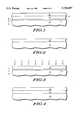
- FIG. 1illustrates, in cross-sectional form, a semiconductor dielectric in accordance with the present invention
- FIGS. 2-3illustrate, in cross-sectional form, a method of forming a semiconductor dielectric in accordance with the present invention
- FIGS. 4-5illustrate, in cross-sectional form, another method of forming a semiconductor dielectric in accordance with the present invention
- FIGS. 6-7illustrate, in cross-sectional form, yet another method of forming a semiconductor dielectric in accordance with the present invention
- FIG. 8illustrates, in cross-sectional form, the semiconductor dielectric of FIG. 1 being used as a transistor gate dielectric
- FIG. 9illustrates, in cross-sectional form, the semiconductor dielectric of FIG. 1 being used to insulate a transistor gate electrode
- FIG. 10illustrates, in cross-sectional form, the semiconductor dielectric of FIG. 1 being used to insulate a first conductive layer from a second conductive layer;
- FIG. 11illustrates, in cross-sectional form, micropore formation in the semiconductor dielectric of FIG. 1;
- FIG. 12illustrates, in cross-sectional form, selective formation of a barrier region adjacent a transistor gate, the formation being in accordance with the present invention.
- a semiconductor dielectric 10In order to form semiconductor dielectric 10, a base layer 12 which has a surface is provided. In most cases, the base layer 12 is a substrate material. Substrate materials include but are not limited to silicon, gallium arsenide, silicon on sapphire, epitaxial formations, germanium, germanium silicon, polysilicon, and/or like substrate materials. In other cases, the base layer may be a transistor gate electrode, a transistor floating gate material for a memory cell, a polysilicon interconnect or layer, amorphous silicon, or a like conductive material. If semiconductor dielectric 10 is formed over a dielectric layer, then the dielectric layer is a base layer. It is important to note that the semiconductor dielectric 10 may be formed either over a base layer or under a base layer.
- an oxynitride layeris formed overlying the base layer 12.
- the oxynitride layerforms a thin interface region referred to as a thin interface layer 13 at the surface of the base layer 12.
- the thin interface layer 13has a substantial or detectable concentration of nitrogen.
- the thin interface layer 13is labeled in FIG. 1 as having a thickness ⁇ .
- the thickness ⁇indicates that the interface layer 13 is a thin layer.
- the thickness ⁇is used in subsequent figures to represent a thin layer or a thin region.
- the oxynitride layeralso forms a thermal oxide layer 14.
- the thermal oxide layer 14is preferably either a wet or dry silicon dioxide (SiO 2 ) material.
- a deposited dielectric layer 16is formed overlying the thermal oxide layer 14.
- Chemical vapor deposition (CVD), plasma enhanced chemical vapor deposition (PECVD), low pressure chemical vapor deposition (LPCVD), or a like deposition processis used to form the deposited dielectric layer 16.
- CVDchemical vapor deposition
- PECVDplasma enhanced chemical vapor deposition
- LPCVDlow pressure chemical vapor deposition
- Many dielectric materials which are formed via depositionare known, but a high temperature oxide (HTO) or a tetraethylorthosilicate (TEOS) based oxide is preferred for the dielectric layer 16.
- a low temperature oxide (LTO)may be used although an LTO may not be as dense or defect-free as an HTO or a TEOS oxide.
- the dielectric layer 16is heated to densify the deposited dielectric layer 16. Densification of the deposited dielectric layer 16 is not always necessary, but will result in a deposited dielectric layer 16 of improved quality.
- the semiconductor dielectric 10 of FIG. 1may be formed via a different method. Instead of using an oxynitride material to form the layers 13 and 14, a fluorinated layer is used to form the layers 13 and 14.
- the base layeris exposed to an ambient containing O 2 and NF 3 or a like fluorine and oxygen containing ambient. Due to the fluorine and oxygen in the ambient, the thin interface layer 13 is formed as a thin region with a thickness of ⁇ .
- the interface layer 13contains a substantial or detectable concentration of fluorine.
- the thermal oxide layer 14forms in a manner that is similar to the oxynitride method discussed above.
- the deposited dielectric layer 16is formed and optionally densified as described above, and the semiconductor dielectric 10 is complete.
- the thin interface layer 13,which has either a high concentration of nitrogen or fluorine allows semiconductor dielectric 10 to be more radiation hard than most known dielectric materials.
- the semiconductor dielectric 10if the thin interface layer 13 is made primarily of nitrogen, reduces or eliminates a known boron penetration problem. Stress is reduced between the base layer 12 and the semiconductor dielectric 10 via the thin interface layer 13.
- FIGS. 2-3illustrate an alternative method that may be used to form the semiconductor dielectric 10.
- the thermal oxide layer 14is grown over the base layer 12 which has a surface. Wet or dry techniques may be used to form the thermal oxide layer 14 as a silicon dioxide layer.
- the thermal oxide layer 14is exposed to an ambient which contains one of either N 2 O or NH 3 , or a like nitrogen containing ambient, to form the thin interface layer 13 which has a substantial concentration of nitrogen.
- the nitrogendiffuses to the surface of the base layer 12 and "piles up" to form the thin interface layer 13.
- deposited dielectric layer 16is formed and optionally densified over the thermal oxide layer 14 in FIG. 3 to form the semiconductor dielectric 10 of FIG. 1.
- an ambient of NF 3 or a like fluorine-containing ambientmay be used in a similar manner to form an interface layer 13 with a substantial concentration of fluorine.
- FIGS. 4-5yet another method for forming the semiconductor dielectric 10 of FIG. 1 is illustrated.
- both the thermal oxide layer 14 and the deposited dielectric layer 16are formed.
- the dielectric layer 16is exposed to an ambient which contains one of either N 2 O or NH 3 , or a like nitrogen containing ambient, to form the thin interface layer 13 that has a substantial concentration of nitrogen.
- the deposited dielectric layer 16is optionally densified as described herein.
- an ambient of NF 3 or a like fluorine-containing ambientmay be used in a similar manner to form the thin interface layer 13 with a substantial concentration of fluorine.
- FIGS. 6-7an ion implantation method of forming the thin interface layer 13 is illustrated.
- a sacrificial dielectric layer 18is formed over the base layer 12.
- the thin interface layer 13does not exist before the formation of the sacrificial dielectric layer 18.
- An ion implantation stepis used to ion implant either nitrogen, fluorine, a nitrogen-containing compound, or a fluorine-containing compound into a region that is near a surface of the base layer 12.
- the implantationalong with an optional heat cycle forms the thin interface layer 13 between the sacrificial dielectric layer 18 and the base layer 12.
- the sacrificial dielectric layer 18is then removed via conventional etch procedures.
- the thermal oxide layer 14 and the deposited dielectric layer 16are formed as discussed herein.
- the layers 14 and 16are formed over the thin interface layer 13.
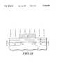
- the semiconductor dielectric 10 of FIG. 1is used as a gate oxide for a field effect transistor (FET).
- FETfield effect transistor
- the layers 13, 14, and 16are formed as described above.
- the base layer 12is a silicon substrate.
- a gate electrode 20is formed overlying the deposited dielectric layer 16 via conventional techniques.
- a source electrode 22 and a drain electrode 24are formed using conventional processing techniques.
- the layers 13 and 14reduce boron penetration between the gate electrode 20 and the base layer 12 when layers 13 and 14 contain nitrogen, reduce stress between the layer 14 and the base layer 12, increase transistor lifetime, increase transistor radiation hardening, reduce breakdown voltage failures, and/or reduce leakage current through layers 13, 14, and 16.
- the layers 13, 14, and 16may be used to form a gate oxide for an electrically erasable programmable read only memory (EEPROM) or an erasable programmable read only memory (EPROM).
- the gate oxideis used to program or erase a floating gate via known tunneling or known hot carrier injection of electrical carriers.
- a set of layers (not illustrated) similar to the layers 13, 14, and 16are optionally used to insulate a floating gate from a control gate.
- the set of layers (not illustrated)are formed overlying an upper surface and adjacent a sidewall of the floating gate in order to insulate the floating gate from the control gate.
- the transistor of FIG. 8is illustrated with additional materials overlying the gate electrode 20.
- a transistoris formed as described in reference to FIG. 8 with semiconductor dielectric 10 functioning as a gate dielectric.
- the gate electrode 20, if made of a silicon-based material,is processed as a base layer via one of the methods described in reference to FIGS. 1-7. This processing forms a thin interface layer 13b which is overlying and surrounding all exposed surfaces of the gate electrode 20.
- Thin interface layer 13bis formed in a manner similar to thin interface layer 13.
- a thermal oxide layer 14bis then formed overlying thin interface layer 13b in a manner that is similar to the formation of thermal oxide layer 14.
- a deposited dielectric layer 16bis formed overlying the thermal oxide layer 14b in a manner that is similar to the formation of deposited dielectric layer 16.
- the layers 13b, 14b, and 16bare formed to prevent boron penetration into or out from the gate electrode 20. In addition, stress exerted on the transistor is reduced.
- FIG. 10illustrates semiconductor dielectric layer 10 which is used as either an inter-polysilicon dielectric layer or an inter-conductor dielectric layer.
- semiconductor dielectric 10is used to isolate a base layer 26, which is a silicon-based material, from a conductive layer 28.
- Conductive layer 28may be either a salicided material, a silicided material, polysilicon, amorphous silicon, single-crystalline silicon, metal, epitaxial silicon, germanium silicon, or a like conductive material. Therefore, the semiconductor dielectric 10 in FIG. 10 is used to isolate a first conductor from a second conductor.
- FIG. 11illustrates how dielectric layer 10 is able to reduce breakdown voltage failures, reduce leakage, and increase lifetime of integrated circuits.
- FIG. 11is a more detailed illustration of FIG. 1.
- FIG. 11illustrates base layer 12, the interface layer 13, thermal oxide layer 14, and deposited dielectric layer 16.
- a defect known as a microporeis usually formed.
- Microporessuch as micropores 30, 32, and 34, are illustrated in FIG. 11. Other micropores are illustrated in FIG. 11, but are not labeled.
- Microporesare defects that occur in thin oxide layers. Many of the micropores form completely from a top surface of a thin oxide layer to a bottom surface of the thin oxide layer, as illustrated via micropores 30 and 32. In some cases, the micropores may only partially form through an oxide layer as illustrated via micropore 34.
- the micropores that run completely through an oxide layerare defects that increase breakdown voltage problems, decrease integrated circuit lifetime, and increase leakage current.
- thermal oxide layer 14results in micropores in the thermal oxide layer 14.
- the formation and optional densification of the deposited dielectric layer 16forms micropores in the deposited dielectric layer 16.
- the micropores in the layer 14are most likely not aligned with the micropores in the layer 16 as illustrated. Therefore, a large number of micropores will not run entirely through the semiconductor dielectric 10.
- the misalignment of defects or misalignment of microporesresults in semiconductor dielectric 10 being more robust than conventional dielectrics and having reduced breakdown voltage problems, reduced integrated circuit lifetime, and reduced leakage current as described herein.
- FIG. 12illustrates a structure having selective formation of a thin interface region.
- the base layer 12is a substrate made of silicon.
- Thermal oxide layer 14 and deposited dielectric layer 16are formed overlying the base layer 12.
- Gate electrode 20, source electrode 22, and drain electrode 24are formed in a conventional manner to form a transistor. The transistor is exposed to either a fluorine-containing or a nitrogen-containing ambient while being heated.
- Thin interface regions 13' and 13" containing a detectable concentration of either nitrogen or fluorineare formed adjacent the gate electrode 20.
- Thin interface regions 13' and 13"are similar to the thin interface region 13 discussed herein for FIGS. 1-11.
- the thin interface regions 13' and 13"are formed at a surface of the base layer 12 and are underlying the thermal oxide layer 14. The extent to which the thin interface regions 13' and 13" extend under the gate electrode will vary based on processing parameters and transistor materials.
- an improved semiconductor dielectric and processing steps for the formation thereofare taught herein.
- the inventive semiconductor dielectricresults in reduced stress, improved integrated circuit lifetime, reduced breakdown voltage failures, reduced boron penetration, improved radiation hardening, and reduced micropore-related problems.
- the semiconductor dielectriccan be used, for example, as a gate dielectric or an inter-conductor dielectric.
- the improved semiconductor dielectriccan be used to protect any type of transistor or may be used to form a gate dielectric for any transistor.
- Lightly doped drain (LDD) regions, elevated source and drain regions, and other known structuresmay be used with the improved semiconductor dielectric.
- the thin interface layers 13, 13', 13", and/or 13b described hereincan be used for other forms of protection.
- the thin interface layers 13, 13', 13", and 13bcan be used to protect underlying layers from hydrogen diffusion. Hydrogen diffusion may occur during passivation, epitaxial growth, or other processing steps.
- the improved semiconductor dielectricmay also be used to protect and insulate thin film transistors (TFTs), silicon on insulator (SOI) transistors, or other silicon based devices.
- TFTsthin film transistors
- SOIsilicon on insulator
- Many dielectric materialsmay be used to form the deposited dielectric layer 16 described herein. It is to be understood, therefore, that this invention is not limited to the particular forms illustrated and that it is intended in the appended claims to cover all modifications that do not depart from the spirit and scope of this invention.
Landscapes
- Engineering & Computer Science (AREA)
- Microelectronics & Electronic Packaging (AREA)
- Condensed Matter Physics & Semiconductors (AREA)
- General Physics & Mathematics (AREA)
- Manufacturing & Machinery (AREA)
- Computer Hardware Design (AREA)
- Physics & Mathematics (AREA)
- Power Engineering (AREA)
- Chemical & Material Sciences (AREA)
- Chemical Kinetics & Catalysis (AREA)
- Crystallography & Structural Chemistry (AREA)
- General Chemical & Material Sciences (AREA)
- Formation Of Insulating Films (AREA)
- Non-Volatile Memory (AREA)
Abstract
Description
Claims (14)
Priority Applications (2)
| Application Number | Priority Date | Filing Date | Title |
|---|---|---|---|
| US08/258,360US5726087A (en) | 1992-04-30 | 1994-06-09 | Method of formation of semiconductor gate dielectric |
| US08/449,964US5712208A (en) | 1994-06-09 | 1995-05-25 | Methods of formation of semiconductor composite gate dielectric having multiple incorporated atomic dopants |
Applications Claiming Priority (2)
| Application Number | Priority Date | Filing Date | Title |
|---|---|---|---|
| US87595992A | 1992-04-30 | 1992-04-30 | |
| US08/258,360US5726087A (en) | 1992-04-30 | 1994-06-09 | Method of formation of semiconductor gate dielectric |
Related Parent Applications (1)
| Application Number | Title | Priority Date | Filing Date |
|---|---|---|---|
| US87595992AContinuation | 1992-04-30 | 1992-04-30 |
Related Child Applications (1)
| Application Number | Title | Priority Date | Filing Date |
|---|---|---|---|
| US08/449,964Continuation-In-PartUS5712208A (en) | 1994-06-09 | 1995-05-25 | Methods of formation of semiconductor composite gate dielectric having multiple incorporated atomic dopants |
Publications (1)
| Publication Number | Publication Date |
|---|---|
| US5726087Atrue US5726087A (en) | 1998-03-10 |
Family
ID=25366670
Family Applications (1)
| Application Number | Title | Priority Date | Filing Date |
|---|---|---|---|
| US08/258,360Expired - LifetimeUS5726087A (en) | 1992-04-30 | 1994-06-09 | Method of formation of semiconductor gate dielectric |
Country Status (1)
| Country | Link |
|---|---|
| US (1) | US5726087A (en) |
Cited By (47)
| Publication number | Priority date | Publication date | Assignee | Title |
|---|---|---|---|---|
| US5837585A (en)* | 1996-07-23 | 1998-11-17 | Vanguard International Semiconductor Corporation | Method of fabricating flash memory cell |
| US5866474A (en)* | 1997-07-17 | 1999-02-02 | United Microelectronics Corp. | Method for manufacturing gate oxide layers |
| US5869370A (en)* | 1997-12-29 | 1999-02-09 | Taiwan Semiconductor Manufacturing Company Ltd. | Ultra thin tunneling oxide using buffer CVD to improve edge thinning |
| US5891798A (en)* | 1996-12-20 | 1999-04-06 | Intel Corporation | Method for forming a High dielectric constant insulator in the fabrication of an integrated circuit |
| US5897358A (en)* | 1997-11-28 | 1999-04-27 | Advanced Micro Devices | Semiconductor device having fluorine-enhanced transistor with elevated active regions and fabrication thereof |
| US5920103A (en)* | 1997-06-20 | 1999-07-06 | Advanced Micro Devices, Inc. | Asymmetrical transistor having a gate dielectric which is substantially resistant to hot carrier injection |
| US5923983A (en)* | 1996-12-23 | 1999-07-13 | Advanced Micro Devices, Inc. | Integrated circuit gate conductor having a gate dielectric which is substantially resistant to hot carrier effects |
| US5998270A (en)* | 1997-05-15 | 1999-12-07 | Advanced Micro Devices | Formation of oxynitride and polysilicon layers in a single reaction chamber |
| US6027992A (en)* | 1997-12-18 | 2000-02-22 | Advanced Micro Devices | Semiconductor device having a gallium and nitrogen containing barrier layer and method of manufacturing thereof |
| US6054374A (en)* | 1997-11-26 | 2000-04-25 | Advanced Micro Devices | Method of scaling dielectric thickness in a semiconductor process with ion implantation |
| WO2000019504A3 (en)* | 1998-09-25 | 2000-07-13 | Conexant Systems Inc | Methods for fabricating interpoly dielectrics in non-volatile stacked-gate memory structures |
| US6215163B1 (en)* | 1997-03-10 | 2001-04-10 | Fujitsu Limited | Semiconductor device and method of manufacturing the same where the nitrogen concentration in an oxynitride insulating layer is varied |
| US6252296B1 (en)* | 1998-09-18 | 2001-06-26 | Mitsubishi Denki Kabushiki Kaisha | Semiconductor device with silicon oxynitride gate insulating film |
| US6261973B1 (en)* | 1997-12-31 | 2001-07-17 | Texas Instruments Incorporated | Remote plasma nitridation to allow selectively etching of oxide |
| US6261976B1 (en) | 1999-03-18 | 2001-07-17 | Chartered Semiconductor Manufacturing Ltd. | Method of forming low pressure silicon oxynitride dielectrics having high reliability |
| US6274442B1 (en)* | 1998-07-15 | 2001-08-14 | Advanced Micro Devices, Inc. | Transistor having a nitrogen incorporated epitaxially grown gate dielectric and method of making same |
| WO2001045501A3 (en)* | 1999-12-21 | 2002-05-10 | Mattson Thermal Products Inc | GROWTH OF ULTRATHIN NITRIDE ON Si(100) BY RAPID THERMAL N2 TREATMENT |
| US6410375B1 (en)* | 1998-07-21 | 2002-06-25 | Samsung Electronics Co., Ltd. | Methods of forming transistors including gate dielectric layers having different nitrogen concentrations |
| KR100349363B1 (en)* | 2000-10-10 | 2002-08-21 | 주식회사 하이닉스반도체 | Method for manufacturing pmos device with high-dielectric constant gate dielectric |
| US6479349B1 (en)* | 1997-07-18 | 2002-11-12 | Sanyo Electric Co., Ltd. | Laser transceiver system controller |
| US6489649B2 (en)* | 1996-12-26 | 2002-12-03 | Hitachi, Ltd. | Semiconductor device having nonvolatile memory and method of manufacturing thereof |
| US6492215B1 (en)* | 1997-08-13 | 2002-12-10 | Citizen Watch Co., Ltd. | Semiconductor device and fabricating the same |
| GB2377548A (en)* | 2001-01-05 | 2003-01-15 | Esm Ltd | TFT fabrication process |
| US6518146B1 (en) | 2002-01-09 | 2003-02-11 | Motorola, Inc. | Semiconductor device structure and method for forming |
| US6534819B2 (en) | 2000-08-30 | 2003-03-18 | Cornell Research Foundation, Inc. | Dense backplane cell for configurable logic |
| US20030072975A1 (en)* | 2001-10-02 | 2003-04-17 | Shero Eric J. | Incorporation of nitrogen into high k dielectric film |
| US6566886B1 (en) | 2001-03-28 | 2003-05-20 | Advanced Micro Devices, Inc. | Method of detecting crystalline defects using sound waves |
| US20030098492A1 (en)* | 2001-11-29 | 2003-05-29 | Singh Rana P. | Semiconductor device structure and method for forming |
| US6639279B1 (en)* | 1999-01-18 | 2003-10-28 | Lg. Philips Lcd Co., Ltd. | Semiconductor transistor having interface layer between semiconductor and insulating layers |
| US6649514B1 (en)* | 2002-09-06 | 2003-11-18 | Lattice Semiconductor Corporation | EEPROM device having improved data retention and process for fabricating the device |
| US6683010B1 (en)* | 1997-06-27 | 2004-01-27 | Samsung Electronics Co., Ltd. | Method for forming silicon-oxynitride layer on semiconductor device |
| US20040051135A1 (en)* | 2002-09-12 | 2004-03-18 | Mosel Vitelic, Inc. | Method for forming a protective buffer layer for high temperature oxide processing |
| US20040058557A1 (en)* | 2002-09-20 | 2004-03-25 | Mattson Technology, Inc. | Method of forming and/or modifying a dielectric film on a semiconductor surface |
| US20040092051A1 (en)* | 2002-10-30 | 2004-05-13 | Amberwave Systems Corporation | Methods for preserving strained semiconductor substrate layers during CMOS processing |
| US20050048705A1 (en)* | 2003-08-26 | 2005-03-03 | International Business Machines Corporation | Method for fabricating a nitrided silicon-oxide gate dielectric |
| US20050059260A1 (en)* | 2003-09-15 | 2005-03-17 | Haowen Bu | CMOS transistors and methods of forming same |
| US20050260347A1 (en)* | 2004-05-21 | 2005-11-24 | Narwankar Pravin K | Formation of a silicon oxynitride layer on a high-k dielectric material |
| US6979658B2 (en)* | 1997-03-06 | 2005-12-27 | Fujitsu Limited | Method of fabricating a semiconductor device containing nitrogen in a gate oxide film |
| EP1731531A2 (en) | 1999-08-09 | 2006-12-13 | EMD Lexigen Research Center Corp. | Multiple cytokine-antibody complexes |
| US20070059948A1 (en)* | 2002-06-14 | 2007-03-15 | Metzner Craig R | Ald metal oxide deposition process using direct oxidation |
| US20070212895A1 (en)* | 2006-03-09 | 2007-09-13 | Thai Cheng Chua | Method and apparatus for fabricating a high dielectric constant transistor gate using a low energy plasma system |
| US20070212896A1 (en)* | 2006-03-09 | 2007-09-13 | Applied Materials, Inc. | Method and apparatus for fabricating a high dielectric constant transistor gate using a low energy plasma system |
| US20070218623A1 (en)* | 2006-03-09 | 2007-09-20 | Applied Materials, Inc. | Method of fabricating a high dielectric constant transistor gate using a low energy plasma apparatus |
| US20080076268A1 (en)* | 2006-09-26 | 2008-03-27 | Applied Materials, Inc. | Fluorine plasma treatment of high-k gate stack for defect passivation |
| CN100380609C (en)* | 2002-01-08 | 2008-04-09 | 马特森技术公司 | UV Enhanced Oxynitridation of Semiconductor Substrates |
| US8828834B2 (en) | 2012-06-12 | 2014-09-09 | Globalfoundries Inc. | Methods of tailoring work function of semiconductor devices with high-k/metal layer gate structures by performing a fluorine implant process |
| US9263270B2 (en) | 2013-06-06 | 2016-02-16 | Globalfoundries Inc. | Method of forming a semiconductor device structure employing fluorine doping and according semiconductor device structure |
Citations (21)
| Publication number | Priority date | Publication date | Assignee | Title |
|---|---|---|---|---|
| US3560810A (en)* | 1968-08-15 | 1971-02-02 | Ibm | Field effect transistor having passivated gate insulator |
| US4003071A (en)* | 1971-09-18 | 1977-01-11 | Fujitsu Ltd. | Method of manufacturing an insulated gate field effect transistor |
| US4282270A (en)* | 1978-10-27 | 1981-08-04 | Fujitsu Limited | Method for forming an insulating film layer of silicon oxynitride on a semiconductor substrate surface |
| JPS56125875A (en)* | 1980-03-06 | 1981-10-02 | Nec Corp | Semiconductor integrated circuit device |
| JPS5817673A (en)* | 1981-07-24 | 1983-02-01 | Toshiba Corp | Field-effect transistor |
| JPS6197866A (en)* | 1984-10-18 | 1986-05-16 | Seiko Epson Corp | MOS type semiconductor memory device |
| US4621277A (en)* | 1978-06-14 | 1986-11-04 | Fujitsu Limited | Semiconductor device having insulating film |
| US4623912A (en)* | 1984-12-05 | 1986-11-18 | At&T Bell Laboratories | Nitrided silicon dioxide layers for semiconductor integrated circuits |
| US4851370A (en)* | 1987-12-28 | 1989-07-25 | American Telephone And Telegraph Company, At&T Bell Laboratories | Fabricating a semiconductor device with low defect density oxide |
| JPH02265279A (en)* | 1989-04-06 | 1990-10-30 | Toshiba Corp | Manufacturing method of semiconductor device |
| JPH0330470A (en)* | 1989-06-28 | 1991-02-08 | Toshiba Corp | Semiconductor device |
| US5034798A (en)* | 1987-07-31 | 1991-07-23 | Kabushiki Kaisha Toshiba | Semiconductor device having a two-layer gate structure |
| US5061647A (en)* | 1990-10-12 | 1991-10-29 | Motorola, Inc. | ITLDD transistor having variable work function and method for fabricating the same |
| US5104819A (en)* | 1989-08-07 | 1992-04-14 | Intel Corporation | Fabrication of interpoly dielctric for EPROM-related technologies |
| US5258333A (en)* | 1992-08-18 | 1993-11-02 | Intel Corporation | Composite dielectric for a semiconductor device and method of fabrication |
| US5286954A (en)* | 1990-12-28 | 1994-02-15 | Fujitsu Limited | Banking terminal having cash dispenser and automatic depository functions |
| US5294820A (en)* | 1986-03-25 | 1994-03-15 | Kabushiki Kaisha Toshiba | Field-effect transistor |
| US5397720A (en)* | 1994-01-07 | 1995-03-14 | The Regents Of The University Of Texas System | Method of making MOS transistor having improved oxynitride dielectric |
| US5407870A (en)* | 1993-06-07 | 1995-04-18 | Motorola Inc. | Process for fabricating a semiconductor device having a high reliability dielectric material |
| US5464783A (en)* | 1993-03-24 | 1995-11-07 | At&T Corp. | Oxynitride-dioxide composite gate dielectric process for MOS manufacture |
| US5591681A (en)* | 1994-06-03 | 1997-01-07 | Advanced Micro Devices, Inc. | Method for achieving a highly reliable oxide film |
- 1994
- 1994-06-09USUS08/258,360patent/US5726087A/ennot_activeExpired - Lifetime
Patent Citations (21)
| Publication number | Priority date | Publication date | Assignee | Title |
|---|---|---|---|---|
| US3560810A (en)* | 1968-08-15 | 1971-02-02 | Ibm | Field effect transistor having passivated gate insulator |
| US4003071A (en)* | 1971-09-18 | 1977-01-11 | Fujitsu Ltd. | Method of manufacturing an insulated gate field effect transistor |
| US4621277A (en)* | 1978-06-14 | 1986-11-04 | Fujitsu Limited | Semiconductor device having insulating film |
| US4282270A (en)* | 1978-10-27 | 1981-08-04 | Fujitsu Limited | Method for forming an insulating film layer of silicon oxynitride on a semiconductor substrate surface |
| JPS56125875A (en)* | 1980-03-06 | 1981-10-02 | Nec Corp | Semiconductor integrated circuit device |
| JPS5817673A (en)* | 1981-07-24 | 1983-02-01 | Toshiba Corp | Field-effect transistor |
| JPS6197866A (en)* | 1984-10-18 | 1986-05-16 | Seiko Epson Corp | MOS type semiconductor memory device |
| US4623912A (en)* | 1984-12-05 | 1986-11-18 | At&T Bell Laboratories | Nitrided silicon dioxide layers for semiconductor integrated circuits |
| US5294820A (en)* | 1986-03-25 | 1994-03-15 | Kabushiki Kaisha Toshiba | Field-effect transistor |
| US5034798A (en)* | 1987-07-31 | 1991-07-23 | Kabushiki Kaisha Toshiba | Semiconductor device having a two-layer gate structure |
| US4851370A (en)* | 1987-12-28 | 1989-07-25 | American Telephone And Telegraph Company, At&T Bell Laboratories | Fabricating a semiconductor device with low defect density oxide |
| JPH02265279A (en)* | 1989-04-06 | 1990-10-30 | Toshiba Corp | Manufacturing method of semiconductor device |
| JPH0330470A (en)* | 1989-06-28 | 1991-02-08 | Toshiba Corp | Semiconductor device |
| US5104819A (en)* | 1989-08-07 | 1992-04-14 | Intel Corporation | Fabrication of interpoly dielctric for EPROM-related technologies |
| US5061647A (en)* | 1990-10-12 | 1991-10-29 | Motorola, Inc. | ITLDD transistor having variable work function and method for fabricating the same |
| US5286954A (en)* | 1990-12-28 | 1994-02-15 | Fujitsu Limited | Banking terminal having cash dispenser and automatic depository functions |
| US5258333A (en)* | 1992-08-18 | 1993-11-02 | Intel Corporation | Composite dielectric for a semiconductor device and method of fabrication |
| US5464783A (en)* | 1993-03-24 | 1995-11-07 | At&T Corp. | Oxynitride-dioxide composite gate dielectric process for MOS manufacture |
| US5407870A (en)* | 1993-06-07 | 1995-04-18 | Motorola Inc. | Process for fabricating a semiconductor device having a high reliability dielectric material |
| US5397720A (en)* | 1994-01-07 | 1995-03-14 | The Regents Of The University Of Texas System | Method of making MOS transistor having improved oxynitride dielectric |
| US5591681A (en)* | 1994-06-03 | 1997-01-07 | Advanced Micro Devices, Inc. | Method for achieving a highly reliable oxide film |
Non-Patent Citations (30)
| Title |
|---|
| "Electrical and Reliability Characteristics of Ultrathin Oxynitride Gate Dielectric Prepared by Rapid Thermal Processing in N2O," by Hwang et al., published in IEDM 1990, pp. 421-424. |
| "Fabrication of Superior Oxynitride Ultrathin MOS Gate dielectrics for ULSI Technology by Rea Rapid Thermal Processing," in SPIE vol. 1189 Rapid Thermal Processing (1989), pp. 186-197. |
| "Fluorine Enhanced Oxidation of Silicon: Effect of Fluorine on Oxide Stress," by Kouvatsos et al. published in Ext. Abs. of the Electrochem. Soc., vol. 90-2, Fall Meeting, Oct., 1992, pp. 447-448. |
| "Improvement in SiO2 Gate Dielectrics with Fluorine Incorporation," by Wright et al., was published in 1988 via the VLSI Symposium 1988, pp. 51-52. |
| "Improvement of Thin-Gate Oxide Integrity Using Through-Silicon-Gate Nitrogen Ion Implantation," IEEE Electron Devices Letters, vol. EDL-8, No. 2, Feb. 1987; Haddad et al. |
| "Improvement of Thin-Gate Oxide Integrity Using Through-Silicon-Gate Nitrogen Ion Implanting," by Haddad et al., published in IEEE Elect. Dev. Letters, vol. EDL-8, No. 2, Feb. 1987, pp. 58-60. |
| "Improvements in Rapid Thermal Oxide/Re-Oxidized Nitrided Oxide (ONO) Films Using NF3", Cable et al., 1991 Mat. Res. Soc. Symp. Proc., vol. 224. |
| "Nitridation Induced Surface Donor Layer in Silicon and It's Impact on the Characteristics of n-and p-Channel MOSFETs", Wu et al, IEEE-IEDM '89, pp. 271-274. |
| "Suppression of Boron Penetration into an Ultra-Thin Gate Oxide by Using a Stacked Amorphous-Silicon (SAS) Film", Wu et al., IEEE-EIDM '93, pp. 329-332. |
| Abbas, S., et al., "Improvement of the Gate-Region Integrity in FET Devices", IBM Tech. Disc. Bull. vol. 14, No. 11, Apr. 1972, pp. 3348-3350. |
| Abbas, S., et al., Improvement of the Gate Region Integrity in FET Devices , IBM Tech. Disc. Bull. vol. 14, No. 11, Apr. 1972, pp. 3348 3350.* |
| Electrical and Reliability Characteristics of Ultrathin Oxynitride Gate Dielectric Prepared by Rapid Thermal Processing in N2O, by Hwang et al., published in IEDM 1990, pp. 421 424.* |
| Fabrication of Superior Oxynitride Ultrathin MOS Gate dielectrics for ULSI Technology by Rea Rapid Thermal Processing, in SPIE vol. 1189 Rapid Thermal Processing (1989), pp. 186 197.* |
| Fluorine Enhanced Oxidation of Silicon: Effect of Fluorine on Oxide Stress, by Kouvatsos et al. published in Ext. Abs. of the Electrochem. Soc., vol. 90 2, Fall Meeting, Oct., 1992, pp. 447 448.* |
| IBM Tech. Disc. Bull., vol. 28, No. 6, Nov. 1985, pp. 2665 2666.* |
| IBM Tech. Disc. Bull., vol. 28, No. 6, Nov. 1985, pp. 2665-2666. |
| Improvement in SiO2 Gate Dielectrics with Fluorine Incorporation, by Wright et al., was published in 1988 via the VLSI Symposium 1988, pp. 51 52.* |
| Improvement of Thin Gate Oxide Integrity Using Through Silicon Gate Nitrogen Ion Implantation, IEEE Electron Devices Letters, vol. EDL 8, No. 2, Feb. 1987; Haddad et al.* |
| Improvement of Thin Gate Oxide Integrity Using Through Silicon Gate Nitrogen Ion Implanting, by Haddad et al., published in IEEE Elect. Dev. Letters, vol. EDL 8, No. 2, Feb. 1987, pp. 58 60.* |
| Improvements in Rapid Thermal Oxide/Re Oxidized Nitrided Oxide (ONO) Films Using NF3 , Cable et al., 1991 Mat. Res. Soc. Symp. Proc., vol. 224.* |
| Li, P.C., et al, Gate Dielectric Structure for Field Effect Transistors IBM Tech. Disc. Bull vol. 17, No. 8, p. 2330.* |
| Nitridation Induced Surface Donor Layer in Silicon and It s Impact on the Characteristics of n and p Channel MOSFETs , Wu et al, IEEE IEDM 89, pp. 271 274.* |
| Research Disclosure, Nov. 1979, Derwent Publications Ltd.; pp. 862 863 No. 18756.* |
| Research Disclosure, Nov. 1979, Derwent Publications Ltd.; pp. 862-863 No. 18756. |
| Suppression of Boron Penetration into an Ultra Thin Gate Oxide by Using a Stacked Amorphous Silicon (SAS) Film , Wu et al., IEEE EIDM 93, pp. 329 332.* |
| Wolf, S. et al., Silicon Processing for the VLSI Era: vol. 1, Process Technology, Lattice Press, 1986, p. 183.* |
| Wolf, S., Silicon Processing for the VLSI Era: vol. 2, Process Integration, Lattice Press, 1990, pp. 273 275.* |
| Wolf, S., Silicon Processing for the VLSI Era: vol. 2, Process Integration, Lattice Press, 1990, pp. 273-275. |
| Wong, S., et al., "Low Pressure Nitrided-Oxide as a thin Gate Dielectric for MOSFETS", J. Electrochem. Soc., vol. 130, No. 5, (1983, May) pp. 1139-1144 (abstract only). |
| Wong, S., et al., Low Pressure Nitrided Oxide as a thin Gate Dielectric for MOSFETS , J. Electrochem. Soc., vol. 130, No. 5, (1983, May) pp. 1139 1144 (abstract only).* |
Cited By (89)
| Publication number | Priority date | Publication date | Assignee | Title |
|---|---|---|---|---|
| US5837585A (en)* | 1996-07-23 | 1998-11-17 | Vanguard International Semiconductor Corporation | Method of fabricating flash memory cell |
| US6306742B1 (en) | 1996-12-20 | 2001-10-23 | Intel Corporation | Method for forming a high dielectric constant insulator in the fabrication of an integrated circuit |
| US5891798A (en)* | 1996-12-20 | 1999-04-06 | Intel Corporation | Method for forming a High dielectric constant insulator in the fabrication of an integrated circuit |
| US5923983A (en)* | 1996-12-23 | 1999-07-13 | Advanced Micro Devices, Inc. | Integrated circuit gate conductor having a gate dielectric which is substantially resistant to hot carrier effects |
| US6596585B2 (en) | 1996-12-26 | 2003-07-22 | Hitachi, Ltd. | Method of manufacturing semiconductor device |
| US20040229476A1 (en)* | 1996-12-26 | 2004-11-18 | Takashi Kobayashi | Method of manufacturing semiconductor device |
| US20030176038A1 (en)* | 1996-12-26 | 2003-09-18 | Takashi Kobayashi | Method of manufacturing semiconductor device |
| US6489649B2 (en)* | 1996-12-26 | 2002-12-03 | Hitachi, Ltd. | Semiconductor device having nonvolatile memory and method of manufacturing thereof |
| US6764902B2 (en) | 1996-12-26 | 2004-07-20 | Renesas Technology Corp. | Method of manufacturing semiconductor device |
| US7075139B2 (en) | 1996-12-26 | 2006-07-11 | Hitachi, Ltd. | Method of manufacturing semiconductor device |
| US7005393B2 (en) | 1997-03-06 | 2006-02-28 | Fujitsu Limited | Method of fabricating a semiconductor device containing nitrogen in an oxide film |
| US6979658B2 (en)* | 1997-03-06 | 2005-12-27 | Fujitsu Limited | Method of fabricating a semiconductor device containing nitrogen in a gate oxide film |
| US6215163B1 (en)* | 1997-03-10 | 2001-04-10 | Fujitsu Limited | Semiconductor device and method of manufacturing the same where the nitrogen concentration in an oxynitride insulating layer is varied |
| US5998270A (en)* | 1997-05-15 | 1999-12-07 | Advanced Micro Devices | Formation of oxynitride and polysilicon layers in a single reaction chamber |
| US5920103A (en)* | 1997-06-20 | 1999-07-06 | Advanced Micro Devices, Inc. | Asymmetrical transistor having a gate dielectric which is substantially resistant to hot carrier injection |
| US6683010B1 (en)* | 1997-06-27 | 2004-01-27 | Samsung Electronics Co., Ltd. | Method for forming silicon-oxynitride layer on semiconductor device |
| US5866474A (en)* | 1997-07-17 | 1999-02-02 | United Microelectronics Corp. | Method for manufacturing gate oxide layers |
| US6479349B1 (en)* | 1997-07-18 | 2002-11-12 | Sanyo Electric Co., Ltd. | Laser transceiver system controller |
| US6492215B1 (en)* | 1997-08-13 | 2002-12-10 | Citizen Watch Co., Ltd. | Semiconductor device and fabricating the same |
| US6054374A (en)* | 1997-11-26 | 2000-04-25 | Advanced Micro Devices | Method of scaling dielectric thickness in a semiconductor process with ion implantation |
| US5897358A (en)* | 1997-11-28 | 1999-04-27 | Advanced Micro Devices | Semiconductor device having fluorine-enhanced transistor with elevated active regions and fabrication thereof |
| US6027992A (en)* | 1997-12-18 | 2000-02-22 | Advanced Micro Devices | Semiconductor device having a gallium and nitrogen containing barrier layer and method of manufacturing thereof |
| US5869370A (en)* | 1997-12-29 | 1999-02-09 | Taiwan Semiconductor Manufacturing Company Ltd. | Ultra thin tunneling oxide using buffer CVD to improve edge thinning |
| US6261973B1 (en)* | 1997-12-31 | 2001-07-17 | Texas Instruments Incorporated | Remote plasma nitridation to allow selectively etching of oxide |
| US6274442B1 (en)* | 1998-07-15 | 2001-08-14 | Advanced Micro Devices, Inc. | Transistor having a nitrogen incorporated epitaxially grown gate dielectric and method of making same |
| US6653180B2 (en) | 1998-07-21 | 2003-11-25 | Samsung Electronics Co., Ltd. | Transistors including gate dielectric layers having different nitrogen concentrations and related structures |
| US6410375B1 (en)* | 1998-07-21 | 2002-06-25 | Samsung Electronics Co., Ltd. | Methods of forming transistors including gate dielectric layers having different nitrogen concentrations |
| US6252296B1 (en)* | 1998-09-18 | 2001-06-26 | Mitsubishi Denki Kabushiki Kaisha | Semiconductor device with silicon oxynitride gate insulating film |
| WO2000019504A3 (en)* | 1998-09-25 | 2000-07-13 | Conexant Systems Inc | Methods for fabricating interpoly dielectrics in non-volatile stacked-gate memory structures |
| US6339000B1 (en) | 1998-09-25 | 2002-01-15 | Conexant Systems, Inc. | Method for fabricating interpoly dielectrics in non-volatile stacked-gate memory structures |
| US6777354B2 (en) | 1999-01-18 | 2004-08-17 | Lg Philips Lcd Co., Ltd. | Semiconductor device and method of manufacturing the same |
| US6639279B1 (en)* | 1999-01-18 | 2003-10-28 | Lg. Philips Lcd Co., Ltd. | Semiconductor transistor having interface layer between semiconductor and insulating layers |
| US20040038463A1 (en)* | 1999-01-18 | 2004-02-26 | Sung Chae Gee | Semiconductor device and method of manufacturing the same |
| US6261976B1 (en) | 1999-03-18 | 2001-07-17 | Chartered Semiconductor Manufacturing Ltd. | Method of forming low pressure silicon oxynitride dielectrics having high reliability |
| EP1731531A2 (en) | 1999-08-09 | 2006-12-13 | EMD Lexigen Research Center Corp. | Multiple cytokine-antibody complexes |
| WO2001045501A3 (en)* | 1999-12-21 | 2002-05-10 | Mattson Thermal Products Inc | GROWTH OF ULTRATHIN NITRIDE ON Si(100) BY RAPID THERMAL N2 TREATMENT |
| US6534819B2 (en) | 2000-08-30 | 2003-03-18 | Cornell Research Foundation, Inc. | Dense backplane cell for configurable logic |
| KR100349363B1 (en)* | 2000-10-10 | 2002-08-21 | 주식회사 하이닉스반도체 | Method for manufacturing pmos device with high-dielectric constant gate dielectric |
| GB2377548B (en)* | 2001-01-05 | 2003-06-18 | Esm Ltd | Method of fabricating a gate dielectric layer for a thin film transistor |
| GB2377548A (en)* | 2001-01-05 | 2003-01-15 | Esm Ltd | TFT fabrication process |
| US6566886B1 (en) | 2001-03-28 | 2003-05-20 | Advanced Micro Devices, Inc. | Method of detecting crystalline defects using sound waves |
| US20030072975A1 (en)* | 2001-10-02 | 2003-04-17 | Shero Eric J. | Incorporation of nitrogen into high k dielectric film |
| US6960537B2 (en)* | 2001-10-02 | 2005-11-01 | Asm America, Inc. | Incorporation of nitrogen into high k dielectric film |
| US7569284B2 (en) | 2001-10-02 | 2009-08-04 | Asm America, Inc. | Incorporation of nitrogen into high k dielectric film |
| US20050212119A1 (en)* | 2001-10-02 | 2005-09-29 | Shero Eric J | Incorporation of nitrogen into high k dielectric film |
| US20080286589A1 (en)* | 2001-10-02 | 2008-11-20 | Asm America, Inc. | Incorporation of nitrogen into high k dielectric film |
| US7405453B2 (en) | 2001-10-02 | 2008-07-29 | Asm America, Inc. | Incorporation of nitrogen into high k dielectric film |
| US7208390B2 (en) | 2001-11-29 | 2007-04-24 | Freescale Semiconductor, Inc. | Semiconductor device structure and method for forming |
| US20030098492A1 (en)* | 2001-11-29 | 2003-05-29 | Singh Rana P. | Semiconductor device structure and method for forming |
| CN100380609C (en)* | 2002-01-08 | 2008-04-09 | 马特森技术公司 | UV Enhanced Oxynitridation of Semiconductor Substrates |
| US6518146B1 (en) | 2002-01-09 | 2003-02-11 | Motorola, Inc. | Semiconductor device structure and method for forming |
| US7569500B2 (en) | 2002-06-14 | 2009-08-04 | Applied Materials, Inc. | ALD metal oxide deposition process using direct oxidation |
| US20070059948A1 (en)* | 2002-06-14 | 2007-03-15 | Metzner Craig R | Ald metal oxide deposition process using direct oxidation |
| US7569501B2 (en) | 2002-06-14 | 2009-08-04 | Applied Materials, Inc. | ALD metal oxide deposition process using direct oxidation |
| US6649514B1 (en)* | 2002-09-06 | 2003-11-18 | Lattice Semiconductor Corporation | EEPROM device having improved data retention and process for fabricating the device |
| US6849897B2 (en)* | 2002-09-12 | 2005-02-01 | Promos Technologies Inc. | Transistor including SiON buffer layer |
| US6893920B2 (en)* | 2002-09-12 | 2005-05-17 | Promos Technologies, Inc. | Method for forming a protective buffer layer for high temperature oxide processing |
| US20040051135A1 (en)* | 2002-09-12 | 2004-03-18 | Mosel Vitelic, Inc. | Method for forming a protective buffer layer for high temperature oxide processing |
| US7101812B2 (en) | 2002-09-20 | 2006-09-05 | Mattson Technology, Inc. | Method of forming and/or modifying a dielectric film on a semiconductor surface |
| US20040058557A1 (en)* | 2002-09-20 | 2004-03-25 | Mattson Technology, Inc. | Method of forming and/or modifying a dielectric film on a semiconductor surface |
| US7208332B2 (en) | 2002-10-30 | 2007-04-24 | Amberwave Systems Corporation | Methods for preserving strained semiconductor substrate layers during CMOS processing |
| US20070042538A1 (en)* | 2002-10-30 | 2007-02-22 | Amberwave Systems Corporation | Methods for preserving strained semiconductor substrate layers during cmos processing |
| US7202121B2 (en) | 2002-10-30 | 2007-04-10 | Amberwave Systems Corporation | Methods for preserving strained semiconductor substrate layers during CMOS processing |
| WO2004102635A3 (en)* | 2002-10-30 | 2005-06-02 | Amberwave Systems Corp | Methods for preserving strained semiconductor layers during oxide layer formation |
| US7071014B2 (en) | 2002-10-30 | 2006-07-04 | Amberwave Systems Corporation | Methods for preserving strained semiconductor substrate layers during CMOS processing |
| US20070161196A1 (en)* | 2002-10-30 | 2007-07-12 | Amberware Systems | Methods for preserving strained semiconductor substrate layers during CMOS processing |
| US20040092051A1 (en)* | 2002-10-30 | 2004-05-13 | Amberwave Systems Corporation | Methods for preserving strained semiconductor substrate layers during CMOS processing |
| US7541208B2 (en) | 2002-10-30 | 2009-06-02 | Amberwave Systems Corporation | Methods for preserving strained semiconductor substrate layers during CMOS processing |
| US20050215069A1 (en)* | 2002-10-30 | 2005-09-29 | Amberwave Systems Corporation | Methods for preserving strained semiconductor substrate layers during CMOS processing |
| US7416909B2 (en) | 2002-10-30 | 2008-08-26 | Amberwave Systems Corporation | Methods for preserving strained semiconductor substrate layers during CMOS processing |
| US20080020551A1 (en)* | 2002-10-30 | 2008-01-24 | Amberwave Systems Corporation | Methods for preserving strained semiconductor substrate layers during CMOS processing |
| US20080014692A1 (en)* | 2003-08-26 | 2008-01-17 | Burnham Jay S | Method for fabricating a nitrided silicon-oxide gate dielectric |
| US7291568B2 (en) | 2003-08-26 | 2007-11-06 | International Business Machines Corporation | Method for fabricating a nitrided silicon-oxide gate dielectric |
| US20050048705A1 (en)* | 2003-08-26 | 2005-03-03 | International Business Machines Corporation | Method for fabricating a nitrided silicon-oxide gate dielectric |
| US8709887B2 (en) | 2003-08-26 | 2014-04-29 | International Business Machines Corporation | Method for fabricating a nitrided silicon-oxide gate dielectric |
| US20060154411A1 (en)* | 2003-09-15 | 2006-07-13 | Haowen Bu | CMOS transistors and methods of forming same |
| US20050059260A1 (en)* | 2003-09-15 | 2005-03-17 | Haowen Bu | CMOS transistors and methods of forming same |
| US20050260347A1 (en)* | 2004-05-21 | 2005-11-24 | Narwankar Pravin K | Formation of a silicon oxynitride layer on a high-k dielectric material |
| US8119210B2 (en) | 2004-05-21 | 2012-02-21 | Applied Materials, Inc. | Formation of a silicon oxynitride layer on a high-k dielectric material |
| US20070218623A1 (en)* | 2006-03-09 | 2007-09-20 | Applied Materials, Inc. | Method of fabricating a high dielectric constant transistor gate using a low energy plasma apparatus |
| US7645710B2 (en) | 2006-03-09 | 2010-01-12 | Applied Materials, Inc. | Method and apparatus for fabricating a high dielectric constant transistor gate using a low energy plasma system |
| US7678710B2 (en) | 2006-03-09 | 2010-03-16 | Applied Materials, Inc. | Method and apparatus for fabricating a high dielectric constant transistor gate using a low energy plasma system |
| US7837838B2 (en) | 2006-03-09 | 2010-11-23 | Applied Materials, Inc. | Method of fabricating a high dielectric constant transistor gate using a low energy plasma apparatus |
| US20070212896A1 (en)* | 2006-03-09 | 2007-09-13 | Applied Materials, Inc. | Method and apparatus for fabricating a high dielectric constant transistor gate using a low energy plasma system |
| US20070212895A1 (en)* | 2006-03-09 | 2007-09-13 | Thai Cheng Chua | Method and apparatus for fabricating a high dielectric constant transistor gate using a low energy plasma system |
| US20080076268A1 (en)* | 2006-09-26 | 2008-03-27 | Applied Materials, Inc. | Fluorine plasma treatment of high-k gate stack for defect passivation |
| US7902018B2 (en) | 2006-09-26 | 2011-03-08 | Applied Materials, Inc. | Fluorine plasma treatment of high-k gate stack for defect passivation |
| US8828834B2 (en) | 2012-06-12 | 2014-09-09 | Globalfoundries Inc. | Methods of tailoring work function of semiconductor devices with high-k/metal layer gate structures by performing a fluorine implant process |
| US9263270B2 (en) | 2013-06-06 | 2016-02-16 | Globalfoundries Inc. | Method of forming a semiconductor device structure employing fluorine doping and according semiconductor device structure |
Similar Documents
| Publication | Publication Date | Title |
|---|---|---|
| US5726087A (en) | Method of formation of semiconductor gate dielectric | |
| US5712208A (en) | Methods of formation of semiconductor composite gate dielectric having multiple incorporated atomic dopants | |
| US5619052A (en) | Interpoly dielectric structure in EEPROM device | |
| US6869848B2 (en) | Method of manufacturing flash memory device | |
| US20040033678A1 (en) | Method and apparatus to prevent lateral oxidation in a transistor utilizing an ultra thin oxygen-diffusion barrier | |
| US20090042347A1 (en) | Method for manufacturing vertical mos transistor | |
| US5998253A (en) | Method of forming a dopant outdiffusion control structure including selectively grown silicon nitride in a trench capacitor of a DRAM cell | |
| US5716891A (en) | Fabrication process of semiconductor device | |
| US6753229B1 (en) | Multiple-thickness gate oxide formed by oxygen implantation | |
| US5927992A (en) | Method of forming a dielectric in an integrated circuit | |
| US6639264B1 (en) | Method and structure for surface state passivation to improve yield and reliability of integrated circuit structures | |
| JPH07123146B2 (en) | Method of manufacturing nonvolatile semiconductor memory device | |
| US5145797A (en) | Method of making semiconductor devices having an implant damage protection film on the gate electrode sidewalls | |
| US6906391B2 (en) | Semiconductor device having silicon oxide film | |
| US5846887A (en) | Method for removing defects by ion implantation using medium temperature oxide layer | |
| KR100281135B1 (en) | Method for forming gate oxide film of semiconductor device | |
| US6828201B1 (en) | Method of manufacturing a top insulating layer for a sonos-type device | |
| US6979658B2 (en) | Method of fabricating a semiconductor device containing nitrogen in a gate oxide film | |
| JPH0992738A (en) | Semiconductor device and manufacturing method thereof | |
| CN115312453B (en) | Method for manufacturing a memory | |
| US6943125B2 (en) | Method for manufacturing semiconductor device | |
| US6716701B1 (en) | Method of manufacturing a semiconductor memory device | |
| KR0167665B1 (en) | Method of forming impurity diffusion barrier layer | |
| US6927150B2 (en) | Method of manufacturing a semiconductor device | |
| KR100266635B1 (en) | Method for fabricating semiconductor oxide |
Legal Events
| Date | Code | Title | Description |
|---|---|---|---|
| STCF | Information on status: patent grant | Free format text:PATENTED CASE | |
| FPAY | Fee payment | Year of fee payment:4 | |
| AS | Assignment | Owner name:FREESCALE SEMICONDUCTOR, INC., TEXAS Free format text:ASSIGNMENT OF ASSIGNORS INTEREST;ASSIGNOR:MOTOROLA, INC.;REEL/FRAME:015698/0657 Effective date:20040404 Owner name:FREESCALE SEMICONDUCTOR, INC.,TEXAS Free format text:ASSIGNMENT OF ASSIGNORS INTEREST;ASSIGNOR:MOTOROLA, INC.;REEL/FRAME:015698/0657 Effective date:20040404 | |
| FPAY | Fee payment | Year of fee payment:8 | |
| AS | Assignment | Owner name:CITIBANK, N.A. AS COLLATERAL AGENT, NEW YORK Free format text:SECURITY AGREEMENT;ASSIGNORS:FREESCALE SEMICONDUCTOR, INC.;FREESCALE ACQUISITION CORPORATION;FREESCALE ACQUISITION HOLDINGS CORP.;AND OTHERS;REEL/FRAME:018855/0129 Effective date:20061201 Owner name:CITIBANK, N.A. AS COLLATERAL AGENT,NEW YORK Free format text:SECURITY AGREEMENT;ASSIGNORS:FREESCALE SEMICONDUCTOR, INC.;FREESCALE ACQUISITION CORPORATION;FREESCALE ACQUISITION HOLDINGS CORP.;AND OTHERS;REEL/FRAME:018855/0129 Effective date:20061201 | |
| FPAY | Fee payment | Year of fee payment:12 | |
| AS | Assignment | Owner name:CITIBANK, N.A., AS COLLATERAL AGENT,NEW YORK Free format text:SECURITY AGREEMENT;ASSIGNOR:FREESCALE SEMICONDUCTOR, INC.;REEL/FRAME:024397/0001 Effective date:20100413 Owner name:CITIBANK, N.A., AS COLLATERAL AGENT, NEW YORK Free format text:SECURITY AGREEMENT;ASSIGNOR:FREESCALE SEMICONDUCTOR, INC.;REEL/FRAME:024397/0001 Effective date:20100413 | |
| AS | Assignment | Owner name:CITIBANK, N.A., AS NOTES COLLATERAL AGENT, NEW YORK Free format text:SECURITY AGREEMENT;ASSIGNOR:FREESCALE SEMICONDUCTOR, INC.;REEL/FRAME:030633/0424 Effective date:20130521 Owner name:CITIBANK, N.A., AS NOTES COLLATERAL AGENT, NEW YOR Free format text:SECURITY AGREEMENT;ASSIGNOR:FREESCALE SEMICONDUCTOR, INC.;REEL/FRAME:030633/0424 Effective date:20130521 | |
| AS | Assignment | Owner name:CITIBANK, N.A., AS NOTES COLLATERAL AGENT, NEW YORK Free format text:SECURITY AGREEMENT;ASSIGNOR:FREESCALE SEMICONDUCTOR, INC.;REEL/FRAME:031591/0266 Effective date:20131101 Owner name:CITIBANK, N.A., AS NOTES COLLATERAL AGENT, NEW YOR Free format text:SECURITY AGREEMENT;ASSIGNOR:FREESCALE SEMICONDUCTOR, INC.;REEL/FRAME:031591/0266 Effective date:20131101 | |
| AS | Assignment | Owner name:FREESCALE SEMICONDUCTOR, INC., TEXAS Free format text:PATENT RELEASE;ASSIGNOR:CITIBANK, N.A., AS COLLATERAL AGENT;REEL/FRAME:037356/0143 Effective date:20151207 Owner name:FREESCALE SEMICONDUCTOR, INC., TEXAS Free format text:PATENT RELEASE;ASSIGNOR:CITIBANK, N.A., AS COLLATERAL AGENT;REEL/FRAME:037354/0225 Effective date:20151207 Owner name:FREESCALE SEMICONDUCTOR, INC., TEXAS Free format text:PATENT RELEASE;ASSIGNOR:CITIBANK, N.A., AS COLLATERAL AGENT;REEL/FRAME:037356/0553 Effective date:20151207 | |
| AS | Assignment | Owner name:MORGAN STANLEY SENIOR FUNDING, INC., MARYLAND Free format text:ASSIGNMENT AND ASSUMPTION OF SECURITY INTEREST IN PATENTS;ASSIGNOR:CITIBANK, N.A.;REEL/FRAME:037486/0517 Effective date:20151207 | |
| AS | Assignment | Owner name:MORGAN STANLEY SENIOR FUNDING, INC., MARYLAND Free format text:ASSIGNMENT AND ASSUMPTION OF SECURITY INTEREST IN PATENTS;ASSIGNOR:CITIBANK, N.A.;REEL/FRAME:037518/0292 Effective date:20151207 | |
| AS | Assignment | Owner name:NXP, B.V., F/K/A FREESCALE SEMICONDUCTOR, INC., NETHERLANDS Free format text:RELEASE BY SECURED PARTY;ASSIGNOR:MORGAN STANLEY SENIOR FUNDING, INC.;REEL/FRAME:040925/0001 Effective date:20160912 Owner name:NXP, B.V., F/K/A FREESCALE SEMICONDUCTOR, INC., NE Free format text:RELEASE BY SECURED PARTY;ASSIGNOR:MORGAN STANLEY SENIOR FUNDING, INC.;REEL/FRAME:040925/0001 Effective date:20160912 | |
| AS | Assignment | Owner name:NXP B.V., NETHERLANDS Free format text:RELEASE BY SECURED PARTY;ASSIGNOR:MORGAN STANLEY SENIOR FUNDING, INC.;REEL/FRAME:040928/0001 Effective date:20160622 | |
| AS | Assignment | Owner name:MORGAN STANLEY SENIOR FUNDING, INC., MARYLAND Free format text:CORRECTIVE ASSIGNMENT TO CORRECT THE REMOVE PATENTS 8108266 AND 8062324 AND REPLACE THEM WITH 6108266 AND 8060324 PREVIOUSLY RECORDED ON REEL 037518 FRAME 0292. ASSIGNOR(S) HEREBY CONFIRMS THE ASSIGNMENT AND ASSUMPTION OF SECURITY INTEREST IN PATENTS;ASSIGNOR:CITIBANK, N.A.;REEL/FRAME:041703/0536 Effective date:20151207 | |
| AS | Assignment | Owner name:SHENZHEN XINGUODU TECHNOLOGY CO., LTD., CHINA Free format text:CORRECTIVE ASSIGNMENT TO CORRECT THE TO CORRECT THE APPLICATION NO. FROM 13,883,290 TO 13,833,290 PREVIOUSLY RECORDED ON REEL 041703 FRAME 0536. ASSIGNOR(S) HEREBY CONFIRMS THE THE ASSIGNMENT AND ASSUMPTION OF SECURITYINTEREST IN PATENTS.;ASSIGNOR:MORGAN STANLEY SENIOR FUNDING, INC.;REEL/FRAME:048734/0001 Effective date:20190217 | |
| AS | Assignment | Owner name:MORGAN STANLEY SENIOR FUNDING, INC., MARYLAND Free format text:CORRECTIVE ASSIGNMENT TO CORRECT THE REMOVE APPLICATION11759915 AND REPLACE IT WITH APPLICATION 11759935 PREVIOUSLY RECORDED ON REEL 037486 FRAME 0517. ASSIGNOR(S) HEREBY CONFIRMS THE ASSIGNMENT AND ASSUMPTION OF SECURITYINTEREST IN PATENTS;ASSIGNOR:CITIBANK, N.A.;REEL/FRAME:053547/0421 Effective date:20151207 | |
| AS | Assignment | Owner name:NXP B.V., NETHERLANDS Free format text:CORRECTIVE ASSIGNMENT TO CORRECT THE REMOVEAPPLICATION 11759915 AND REPLACE IT WITH APPLICATION11759935 PREVIOUSLY RECORDED ON REEL 040928 FRAME 0001. ASSIGNOR(S) HEREBY CONFIRMS THE RELEASE OF SECURITYINTEREST;ASSIGNOR:MORGAN STANLEY SENIOR FUNDING, INC.;REEL/FRAME:052915/0001 Effective date:20160622 | |
| AS | Assignment | Owner name:NXP, B.V. F/K/A FREESCALE SEMICONDUCTOR, INC., NETHERLANDS Free format text:CORRECTIVE ASSIGNMENT TO CORRECT THE REMOVEAPPLICATION 11759915 AND REPLACE IT WITH APPLICATION11759935 PREVIOUSLY RECORDED ON REEL 040925 FRAME 0001. ASSIGNOR(S) HEREBY CONFIRMS THE RELEASE OF SECURITYINTEREST;ASSIGNOR:MORGAN STANLEY SENIOR FUNDING, INC.;REEL/FRAME:052917/0001 Effective date:20160912 |