US5724284A - Multiple bits-per-cell flash shift register page buffer - Google Patents
Multiple bits-per-cell flash shift register page bufferDownload PDFInfo
- Publication number
- US5724284A US5724284AUS08/669,116US66911696AUS5724284AUS 5724284 AUS5724284 AUS 5724284AUS 66911696 AUS66911696 AUS 66911696AUS 5724284 AUS5724284 AUS 5724284A
- Authority
- US
- United States
- Prior art keywords
- latch
- page buffer
- output
- bit line
- input
- Prior art date
- Legal status (The legal status is an assumption and is not a legal conclusion. Google has not performed a legal analysis and makes no representation as to the accuracy of the status listed.)
- Expired - Lifetime
Links
- 239000000872bufferSubstances0.000titleclaimsabstractdescription53
- 239000000758substrateSubstances0.000description7
- 238000010586diagramMethods0.000description6
- 238000000034methodMethods0.000description5
- 239000004065semiconductorSubstances0.000description5
- 101000833350Homo sapiens Phosphoacetylglucosamine mutaseProteins0.000description3
- 102100024440Phosphoacetylglucosamine mutaseHuman genes0.000description3
- 101000583553Homo sapiens Phosphoglucomutase-1Proteins0.000description2
- 101001072903Homo sapiens Phosphoglucomutase-2Proteins0.000description2
- 102100030999Phosphoglucomutase-1Human genes0.000description2
- 102100036629Phosphoglucomutase-2Human genes0.000description2
- 239000002784hot electronSubstances0.000description2
- 238000012986modificationMethods0.000description2
- 230000004048modificationEffects0.000description2
- 230000004044responseEffects0.000description2
- 101100293180Arabidopsis thaliana MYB28 geneProteins0.000description1
- 230000005689Fowler Nordheim tunnelingEffects0.000description1
- 102100029768Histone-lysine N-methyltransferase SETD1AHuman genes0.000description1
- 101000865038Homo sapiens Histone-lysine N-methyltransferase SETD1AProteins0.000description1
- 101100020366Mus musculus Krtap14 geneProteins0.000description1
- 108010075750P-Type Calcium ChannelsProteins0.000description1
- 230000005684electric fieldEffects0.000description1
- 238000005516engineering processMethods0.000description1
- 230000006870functionEffects0.000description1
- 238000002347injectionMethods0.000description1
- 239000007924injectionSubstances0.000description1
- 238000004519manufacturing processMethods0.000description1
- 239000000463materialSubstances0.000description1
Images


Classifications
- G—PHYSICS
- G11—INFORMATION STORAGE
- G11C—STATIC STORES
- G11C11/00—Digital stores characterised by the use of particular electric or magnetic storage elements; Storage elements therefor
- G11C11/56—Digital stores characterised by the use of particular electric or magnetic storage elements; Storage elements therefor using storage elements with more than two stable states represented by steps, e.g. of voltage, current, phase, frequency
- G11C11/5621—Digital stores characterised by the use of particular electric or magnetic storage elements; Storage elements therefor using storage elements with more than two stable states represented by steps, e.g. of voltage, current, phase, frequency using charge storage in a floating gate
- G11C11/5642—Sensing or reading circuits; Data output circuits
- G—PHYSICS
- G11—INFORMATION STORAGE
- G11C—STATIC STORES
- G11C11/00—Digital stores characterised by the use of particular electric or magnetic storage elements; Storage elements therefor
- G11C11/56—Digital stores characterised by the use of particular electric or magnetic storage elements; Storage elements therefor using storage elements with more than two stable states represented by steps, e.g. of voltage, current, phase, frequency
- G11C11/5621—Digital stores characterised by the use of particular electric or magnetic storage elements; Storage elements therefor using storage elements with more than two stable states represented by steps, e.g. of voltage, current, phase, frequency using charge storage in a floating gate
- G11C11/5628—Programming or writing circuits; Data input circuits
- G—PHYSICS
- G11—INFORMATION STORAGE
- G11C—STATIC STORES
- G11C19/00—Digital stores in which the information is moved stepwise, e.g. shift registers
- G—PHYSICS
- G11—INFORMATION STORAGE
- G11C—STATIC STORES
- G11C2211/00—Indexing scheme relating to digital stores characterized by the use of particular electric or magnetic storage elements; Storage elements therefor
- G11C2211/56—Indexing scheme relating to G11C11/56 and sub-groups for features not covered by these groups
- G11C2211/564—Miscellaneous aspects
- G11C2211/5642—Multilevel memory with buffers, latches, registers at input or output
- G—PHYSICS
- G11—INFORMATION STORAGE
- G11C—STATIC STORES
- G11C8/00—Arrangements for selecting an address in a digital store
- G11C8/04—Arrangements for selecting an address in a digital store using a sequential addressing device, e.g. shift register, counter
Definitions
- This inventionrelates generally to floating gate memory devices such as an array of flash electrically erasable programmable read-only memory (EEPROM) cells. More particularly, it relates to a shift register page buffer for use in an array of multiple bits-per-cell flash EEPROM memory cells so as to render page mode programming and reading.
- EEPROMelectrically erasable programmable read-only memory
- Flash EPROMelectrically erasable EPROMs/EEPROMs
- a plurality of one-transistor flash EEPROM core cellsmay be formed on a semiconductor substrate in which each cell is comprised of a P-type conductivity substrate, an N-type conductivity source region formed integrally with the substrate, and an N-type conductivity drain region also formed integrally within the substrate.
- a floating gateis separated from the substrate by a thin dielectric layer.
- a second dielectric layerseparates a control gate from the floating gate.
- a P-type channel region in the substrateseparates the source and drain regions.
- the drain region and the control gateare raised to predetermined potentials above the potential applied to the source region.
- the drain regionhas applied thereto a voltage V D of approximately +5.5 volts with the control gate V G having a voltage of approximately +12 volts applied thereto.
- V Dvoltage of approximately +5.5 volts
- V Gvoltage of approximately +12 volts applied thereto.
- a positive potentiale.g., +5 volts
- the control gateis at a negative potential (e.g., -8 volts), and the drain region is allowed to float.
- a strong electric fielddevelops between the floating gate and the source region, and a negative charge is extracted from the floating gate to the source region by way of Fowler-Nordheim tunneling.
- the magnitude of the read currentis measured.
- the source regionis held at a ground potential (0 volts) and the control gate is held at a potential of about +5 volts.
- the drain regionis held at a potential between +1 to +2 volts.
- a master bandgap voltage reference generator circuitis used to selectively generate one of a plurality of target memory core cell bit line program-verify voltages, each one corresponding to one of the programmable memory states.
- a switching circuitselectively connects a program current source to the array bit lines containing the selected memory core cells which are to be programmed.
- a sensing logic circuitcompares continuously the potential on the array bit line with one of the target bit line program-verify voltages.
- the switching circuitdisconnects the program current source so as to inhibit further programming when the potential on the bit line falls below the selected one of the plurality of target bit line program-verify voltages.
- the page buffer of the present inventionis utilized in the multiple bits-per-cell EEPROM memory cell array programming and reading techniques described in the aforementioned Ser. Nos. 08/688,795 and 08/635,995, which are hereby incorporated by reference.
- the output of the latch driven by the sense amplifier of the read circuitrycontains the stored information based upon the comparison of the array bit line voltage and a target reference cell bit line voltage. This stored information is later clocked into a shift register of the instant page buffer.
- program logic patterns corresponding to the desired programmable memory statesare shifted serially into the shift register, which controls whether to allow programming of the selected memory cell or to inhibit programming of the same.
- a page bufferfor use in an array of multiple bits-per-cell flash EEPROM memory cells so as to render page mode programming and reading.
- a sensing circuitis provided for selectively and sequentially comparing bit line voltages with each of the plurality of reference voltages.
- a shift register circuitis responsive to the sensing circuit for sequentially storing either a low or high logic level after each comparison of the bit line voltages with one of the plurality of reference voltages.
- the shift register circuitis formed of a plurality of series-connected latch circuits, each having an input and an output.
- a switching circuitis interconnected between the sensing circuit and the latch circuits and is responsive to a corresponding one of the latch outputs for selectively passing the logic signal from the sensing circuit to the input of the latch means.
- the shift register circuitincludes an inhibit program circuit which is responsive to certain outputs of the latch means for generating an inhibit logic signal so as to prevent programming.
- the latch meansare loaded with data corresponding to memory state regions to be programmed into the selected memory cells.
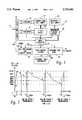
- FIG. 1is a block diagram of a multiple bits-per-cell semiconductor integrated circuit memory device having page buffer circuitry, constructed in accordance with the principles of the present invention
- FIG. 2illustrates the four memory state regions for a two bits-per-cell EEPROM memory cell which stores two bits of data per cell, there being three target reference cell threshold voltages and three target program threshold voltages;
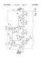
- FIG. 3is a simplified block diagram of the page buffer 38 of FIG. 1 and associated circuitry in the blocks 110, 36 and 40;
- FIGS. 4(a) and 4(b), when connected together,is a detailed schematic circuit diagram of the various blocks in FIG. 3;
- FIG. 5is a graph of the bit line voltage as a function of the programming time corresponding to the three programmed states B, C, and D of FIG. 2, useful in understanding the programming operation of the present invention.
- FIG. 1a block diagram of a multiple bits-per-cell semiconductor integrated circuit memory device 10 which includes a shift register page buffer so as to render page mode programming and reading operations in an array of multiple bits-per-cell flash electrically erasable read-only memory (EEPROM) cells of the memory device.
- the shift register page buffer 38 and the remaining portions of the memory device 10are both wholly formed on a single semi-conductor substrate by known CMOS integrated circuit technology.
- the multiple bits-per-cell semiconductor integrated circuit memory device 10includes a memory core cell array 12, a row address decoder 14, a column address decoder 16, an address input circuit 18, a Y-pass gate circuit 20, a reference cell array 22, a reference Y-select circuit 24, read circuitry 110, and a bit line pre-charge and current source circuitry 36.
- Address signals A jare applied externally to the address input circuit 18.
- the row address signals from the address input circuit 18are fed to the row address decoder 14, and the column address signals thereof are fed to the column address decoder 16.
- the row address decoder 14selects certain ones of the plurality of word lines in the memory core cell array 12 in response to the row address signals.
- the column address decoder 16selects one of the pages in the memory core array in response to the column address signals as well as corresponding sets of reference columns associated with the selected page.
- the details of the read circuitry 110 and associated componentsare described and illustrated in the aforementioned application Ser. No. 08/688,795. Further, the details of the bit line pre-charge and current source circuitry 36 and associated components are described and illustrated in the aforementioned Ser. No. 08/635,995.
- the page buffer 38 and extended NOR gate circuitry 40 of the present inventionare utilized in conjunction with the programming and reading circuits and techniques in these previously mentioned applications.
- the read circuitrycontains the stored information based upon the comparison of the array bit line voltages and the target reference cell bit line voltages, which stored information is later clocked into shift registers of the instant page buffer.
- program logic patterns corresponding to the desired target program statesare shifted serially into the shift registers of the page buffer, which controls whether to allow programming of the selected memory cells or to inhibit programming of the same.
- FIG. 2there is shown a graph of the three reference cell threshold voltages REFVT1, REFVT2, and REFVT3 which serves to divide the programmable threshold range of a two bits-per-cell EEPROM memory cell into four memory state regions (one erased region and three programmable regions).
- the first or erased memory state regionis referred to as logic pattern "11.”
- the second or first programmable memory state regionis referred to as logic pattern “10.”
- the third or second programmable memory state regionis referred to as logic pattern "01.”
- the fourth or third programmable memory state regionis referred to as logic pattern "00.”
- the first reference cell threshold voltage REFVT1separates the logic patterns “11” and “10.”
- the second reference cell threshold voltage REFVT2separates the logic patterns “10” and "01.”
- the third reference cell threshold voltage REFVT3separates the logic patterns "01” and "00.”
- FIG. 3there is illustrated a simple block diagram of the shift register page buffer 38 of FIG. 1 and the portions of the associated circuitry in the read circuitry block 110, bit line pre-charge and current source circuitry block 36, and the extended NOR gate circuit block 40.
- the shift register page buffer 38is comprised of two series-connected shift register elements 300, a switch circuit portion 310, and an inhibit program circuit portion 312.
- the first shift register 300is formed of series-connected latches 302 and 304.
- the second shift register 300is formed of series-connected latches 306 and 308.
- a serial input data line 314is used to connect the output of a preceding page buffer associated with an adjacent bit line to the input of the first latch 302 in the first shift register 300.
- the output of the first latch 302 on line 316is connected to the input of the second latch 304 whose output on line 318 is connected to the input of the third latch 306.
- the output of the third latch 306 on line 320is connected to the input of the fourth latch 308.
- a serial output data line 322is used to connect the output of the fourth latch 308 to the input of a next succeeding page buffer associated with an adjacent bit line.
- the inhibit program circuit portion 312has a first input on line 324 connected to the output of the first latch 302 and a second input on line 326 connected to the output of the third latch 306.
- the output of the inhibit program circuitis connected via line 328 to another input of the latch 27 in the read circuitry 110.
- the switch circuit portion 310has a first terminal on line 330 connected to the output of the latch 27 and a second terminal on line 332 connected also to the output of the third latch 306.
- the switch circuit portion 310has a third terminal on line 334 which is connected to a second input of the first latch 302.
- the read circuitry 110contains the differential pair amplifier 26 and the latch 27.
- the differential amplifier 26has its inverting input connected to a node 336 and to the bit line BL from the memory core cell array 12 and its non-inverting input connected to a line 338 for receiving either a bandgap derived reference voltage BGR or the reference bit line voltage REFBLX.
- the output of the differential pair amplifier 26is fed to the input of the latch 27 whose output defines the output of the read circuitry 110.
- the output of the latch 27is fed via line 340 to the input of the bit line pre-charge and current source circuitry 36, via the line 330 to the input of the page buffer 38, and via line 342 to the input of the NOR gate circuitry 40.
- the current source circuitry 36has a first input on line 344 for receiving the program high voltage VPROG, a second input on line 346 for receiving a read voltage, and a third input on line 348 for receiving a current source enable voltage.
- the output of the current source circuity 36is on line 350 which is fed to the inverting input of the differential pair amplifier 26 via the node 336.
- the NOR gate circuitry 40is used for generating a signal VERIFY on line 41 which goes to a high logic level when the whole page has been verified.
- the first latch 302is formed of a pass transistor N1 and a pair of cross-coupled inverters I1 and I2.
- the second latch 304is formed of a pass transistor N2 and a pair of cross-coupled inverters I3 and I4.
- the third latch 306is formed of a pass transistor N3 and a pair of cross-coupled inverters I5 and I6, and the fourth latch 308 is formed of a pass transistor N4 and a pair of cross-coupled inverters I7 and I8.
- the inhibit program circuit portion 312includes three series-connected P-channel transistors P1, P2 and P3 connected between the power supply potential VCC and the line 328 which is connected to the input of the latch 27.
- the transistor P1has its source connected to the power supply potential VCC, its gate connected to a program enable signal PE and its drain connected to the source of the transistor P2.
- the transistor P2has its gate connected to the input of the inverter I7 and its drain connected to the source of the transistor P3.
- the drain of the transistor P3is connected to the line 328.
- the switch circuit portion 310is formed of an N-channel transistor N5 having its drain/source conduction path connected between the output of the latch 27 (line 330) and the second input of the first latch 302 (line 334). The gate of the transistor N5 is connected to the input of the inverter I7.
- the gate of the transistor N14 defining the input of the current source circuitry 36 on the line 340is connected to the output of the latch 27.
- the drain of the transistor N14is connected to the line 350 defining the output of the current source circuitry 36.
- the source of the transistor P8is connected to the program high voltage VPROG, and the gate of the transistor N15 is connected to the line 348 for receiving the current source enable signal.
- the extended NOR gate circuit block 40is comprised of a plurality of identical verify circuits 40a, one of which is shown in detail.
- Each of the verify circuits 40aincludes series-connected pull-up transistor P10 and pull-down transistor N16.
- the pull-up transistor P10has its source connected to the power supply potential VCC, its gate connected to a common load signal, and its drain connected to the drain of the pull-down transistor N16.
- the gate of the transistor N16is connected to the output of the latch 27 via the line 342, and the source thereof is connected to the ground potential.
- the common node 352 of the transistors P10 and N16is connected to all of the other common nodes in the plurality of verify circuits 40a so as to place them in a parallel arrangement.
- the common node 352is further connected to the output line 41 so as to produce the signal VERIFY.
- the outputs of all of the latches 302-308 of the shift registersare set to zero.
- the read signal READ on the gate of the transistor N13will be made high so as to precharge all of the bit lines BL to the same potential (i.e., +1.5 V) prior to the start of the read mode.
- the program high voltage VPROGwill be set equal to the power supply potential VCC during the read mode. The read operation is described and illustrated in the aforementioned application Ser. No. 08/688,795.
- the second reference threshold level REFVT2 programmed into the corresponding one of the associated reference core cellsis selected to be used as the reference voltage REFBLX defining a target reference cell bit line voltage on the line 338. Since the voltage on the bit line corresponding to the third programmable memory state region will be higher than the second reference threshold level REFVT2, the output of the differential pair amplifier 26 will be low and the output of the latch 27 will store a logic "1.”
- the output of the inverter I1will store a logic "0.” Thereafter, the gate of the transistor N2 will receive the signal CLKB so as to shift the MSB from the output of the first latch 302 (inverter I1) to the output of the second latch 304 (inverter I3).
- a second read step operationis performed by initially precharging again all of the bit lines to the same potential prior to start of the second read mode. Further, the gate of the pass transistor N3 receives the signal CLK so as to further shift the MSB from the output of the second latch 304 to the output of the third latch 306 (inverter I5).
- the first reference threshold level REFVT1 programmed into the corresponding one of the associated reference core cellsis selected to be used this time as the reference voltage REFBLX on the line 338.
- the output of the differential pair amplifier 26will again be low and the output of the latch 27 will store a logic "1.” Again, the output of the latch 27 is transferred into the first latch 302 by the transistor N5. Thus, the output of the inverter I1 will store a logic "0.” Thereafter, the gate of the pass transistors N2 and N4 will receive the signal CLKB so as to shift the MSB from the output of the third latch 306 (inverter I5) to the output of the fourth latch 308 (inverter I7) and to shift result of the second read step stored in the first latch to the second latch.
- a third read stepis performed by initially pre-charging once again all of the bit lines to the same potential prior to the start of the third read mode.
- the third reference threshold level REFVT3 programmed into the corresponding one of the associated reference core cellsis selected to be used this time as the reference voltage REFBLX on the line 338. Since the bit line voltage corresponding to the third programmed memory state region will be higher than the third reference threshold level REFVT3, the output of the differential pair amplifier 26 will be low and the output of the latch 27 will store a logic "1.”
- the least significant bitis shifted from the first latch 302 to the second latch 304.
- the outputs of the first and second latches 302, 304will be storing the LSB, and the outputs of the third and fourth latches 306, 308 will be storing the MSB.
- the data or logic pattern "stored in the latches"will be shifted serially out from the shift registers via the serial data output line 322 after the whole page has been read.
- the signal SET1 on the gate of the transistor N18is made high.
- the logic "0" at the output of the inverter I1is passed through to the input of the inverter I7 by clocking the signals CLK and CLKB. This causes the output of the latch 27 on the line 340 to go low ("0").
- the corresponding bit line BL on the pageis pre-charged by the program inhibit high voltage VPROG (approximately 5-6 V) via the transistors P8 and P9.
- VPROGapproximately 5-6 V
- the common array ground line VSSis also charged to the same high voltage.
- a page of data to be programmedis loaded serially into the page buffers 38 associated with the bit lines in the page through the serial input data line 314.
- the first and second latches 302, 304are loaded with "0,” and the third and fourth latches are also loaded with “0.” Then signal REL will go high so as to cause the output of the latch 27 to go high ("1"). Consequently, the current source will be switched on due to the conduction of the transistor N14.
- the programmingwill begin when the voltage on the word line WL 1 is charged up to the voltage VPP. However, if the page buffer 38 is loaded with "11" data (the outputs of the inverters I3 and I7) corresponding to the erased memory state region, then the inhibit programming circuit 312 will cause the output of the latch 27 to be switched to the logic "0" corresponding to a verified state. Accordingly, the current source will be turned off and no programming will occur.
- an external logic controller 354will cause the first target program memory state level PGM1 to be set or applied as the reference voltage BGR to the gate of the input transistor N7.
- the memory cell MC 11will be charging or programming until the bit line voltage falls below the first reference memory programmed state level PMG1.
- the output of the differential pair amplifier 26will go high and the output of the latch 27 will be switched to a logic "0,” thereby turning off the current source I S and charging the bit line back to the program high voltage VPROG. This is the program inhibit state.
- the memory cells that are not required to be programmed beyond the first reference programmed memory stateare inhibited. This occurs after the external logic controller 354 has caused the shift registers to be loaded with a next set of data in accordance with the Table listed below.
- the new data listed in the Tableis generated by clocking out serially the entire contents of the page buffer shift register bit-by-bit, passing the data through the external logic controller 354, and reentering the data bit-by-bit back into the page buffer shift register.
- the data of "11"means that programming is to be inhibited. Any other pattern data means that programming is allowed to continue up one more level.
- the external logic controller 354will cause the second reference programmed memory state level PGM2 to be applied as a reference voltage BGR to the gate of the transistor N7. Thereafter, the memory cell MC 11 will continue to program until the bit line voltage falls below the second reference program memory state level. At that time, the latch 27 will again be switched to a logic "0" in order to switch off the current source and further programming. The bit line voltage will again be charged back to the program inhibit high voltage VPROG. After all of the bit lines in the page that are to be programmed to the second program memory state region (logic pattern "01"), then the output signal VERIFY on the line 41 will go high. The memory cells that are not required to be programmed beyond the second level are inhibited.
- the external logic controller 354will load the shift register with the next set of data (i.e., logic "10") which causes the third reference program memory state level PGM3 to be applied as the reference voltage BGR to the gate of the input transistor N7. Consequently, the memory cell MC 11 will continue to program until the bit line voltage falls below the third reference programmed memory state level. At that time, the latch 27 will again be switched to a logic "0" in order to switch off the current source and inhibit further programming. The bit line will again be charged back to the program high voltage VPROG. Lastly, after all of the bit lines in the page that are to be programmed to the third program memory state region (logic pattern "00"), then the output signal VERIFY on the line 41 will go high. The signal ISO on the gate of the transistor N17 serves to isolate the shift register from the latch 27 during programming.
- the next set of datai.e., logic "10"
- the present inventionprovides a shift register page buffer for use in an array of multiple bits-per-cell flash EEPROM memory cells so as to render page mode programming and reading.
- a sensing logic circuitis provided for selectively and sequentially comparing the array bit line voltages with a plurality of target reference cell bit line voltages.
- a shift register circuitis responsive to the sensing circuit for sequentially storing either a low or high logic level after each comparison of the bit line voltages with each of the plurality of target cell bit line reference voltages.
- the shift register circuitis formed of series-connected latch circuits having inputs and outputs.
Landscapes
- Engineering & Computer Science (AREA)
- Computer Hardware Design (AREA)
- Read Only Memory (AREA)
Abstract
Description
TABLE ______________________________________ Desired Programmed Program Step Program Step Program Step Memory State Level No. 1 No. 2 No. 3 ______________________________________ Erased 11 11 11 PGM1 10 11 11 PGM2 01 10 11 PGM3 00 01 10 ______________________________________
Claims (18)
Priority Applications (5)
| Application Number | Priority Date | Filing Date | Title |
|---|---|---|---|
| US08/669,116US5724284A (en) | 1996-06-24 | 1996-06-24 | Multiple bits-per-cell flash shift register page buffer |
| PCT/US1997/001874WO1997050090A1 (en) | 1996-06-24 | 1997-01-31 | A multiple bits-per-cell flash shift register page buffer |
| EP97905795AEP0907955B1 (en) | 1996-06-24 | 1997-01-31 | A multiple bits-per-cell flash shift register page buffer |
| DE69702195TDE69702195T2 (en) | 1996-06-24 | 1997-01-31 | SLIDING REGISTER FLASH SIDE BUFFER WITH SEVERAL BITS PER CELL |
| TW086101386ATW364997B (en) | 1996-06-24 | 1997-02-05 | A multiple bits-per-cell flash shift register page buffer |
Applications Claiming Priority (1)
| Application Number | Priority Date | Filing Date | Title |
|---|---|---|---|
| US08/669,116US5724284A (en) | 1996-06-24 | 1996-06-24 | Multiple bits-per-cell flash shift register page buffer |
Publications (1)
| Publication Number | Publication Date |
|---|---|
| US5724284Atrue US5724284A (en) | 1998-03-03 |
Family
ID=24685094
Family Applications (1)
| Application Number | Title | Priority Date | Filing Date |
|---|---|---|---|
| US08/669,116Expired - LifetimeUS5724284A (en) | 1996-06-24 | 1996-06-24 | Multiple bits-per-cell flash shift register page buffer |
Country Status (5)
| Country | Link |
|---|---|
| US (1) | US5724284A (en) |
| EP (1) | EP0907955B1 (en) |
| DE (1) | DE69702195T2 (en) |
| TW (1) | TW364997B (en) |
| WO (1) | WO1997050090A1 (en) |
Cited By (22)
| Publication number | Priority date | Publication date | Assignee | Title |
|---|---|---|---|---|
| US5973967A (en)* | 1997-01-03 | 1999-10-26 | Programmable Microelectronics Corporation | Page buffer having negative voltage level shifter |
| US5995413A (en)* | 1998-01-09 | 1999-11-30 | Information Storage Devices, Inc. | Trimbit circuit for flash memory integrated circuits |
| US6002611A (en)* | 1998-07-22 | 1999-12-14 | Halo Lsi Design & Device Technology, Inc. | Fast, low current program with auto-program for flash memory |
| US6065760A (en)* | 1998-07-06 | 2000-05-23 | Weygandt; James H. | Interchangeable skate wheel bearing assembly |
| US20010021958A1 (en)* | 1999-12-22 | 2001-09-13 | Stmicroelectronics S.A. | Page by page programmable flash memory |
| US6411551B1 (en)* | 1999-11-01 | 2002-06-25 | Samsung Electronics Co., Ltd. | Multi-state nonvolatile semiconductor memory device which is capable of regularly maintaining a margin between threshold voltage distributions |
| US20030068607A1 (en)* | 2001-07-16 | 2003-04-10 | Immersion Corporation | Interface apparatus with cable-driven force feedback and four grounded actuators |
| US20030117856A1 (en)* | 2001-07-23 | 2003-06-26 | Samsung Electronics Co., Ltd. | Memory devices with page buffer having dual registers and method of using the same |
| WO2003069627A1 (en)* | 2002-02-11 | 2003-08-21 | Advanced Micro Devices, Inc. | Partial page programming of multi level flash semiconductor memory |
| US20040141374A1 (en)* | 2003-01-21 | 2004-07-22 | Nexflash Technologies, Inc. | Nonvolatile memory integrated circuit having volatile utility and buffer memories, and method of operation thereof |
| US20040170058A1 (en)* | 2002-01-18 | 2004-09-02 | Gonzalez Carlos J. | Reducing the effects of noise in non-volatile memories through multiple reads |
| WO2004053888A3 (en)* | 2002-12-09 | 2004-09-30 | Sandisk Corp | Zone boundary adjustment for defects in non-volatile memories |
| US20050013171A1 (en)* | 2003-06-17 | 2005-01-20 | Amir Ban | Methods of increasing the reliability of a flash memory |
| US20060013045A1 (en)* | 2004-07-15 | 2006-01-19 | Hynix Semiconductor Inc. | Page buffer of non-volatile memory device and method of programming and reading non-volatile memory device |
| US20060039197A1 (en)* | 2004-05-20 | 2006-02-23 | Stmicroelectronics S.R.I. | Page buffer for a programmable memory device |
| US20080080260A1 (en)* | 2006-09-29 | 2008-04-03 | Hynix Semiconductor Inc. | Page buffer circuit of memory device and program method |
| US20090257422A1 (en)* | 2008-03-10 | 2009-10-15 | Smith R Clayton | Time slot synchronized, flexible bandwidth communication system |
| US20100034643A1 (en)* | 2008-08-06 | 2010-02-11 | General Electric Company | Transition duct aft end frame cooling and related method |
| US20110157993A1 (en)* | 2009-12-31 | 2011-06-30 | Hynix Semiconductor Inc. | Semiconductor memory device and read method thereof |
| DE102005038861B4 (en)* | 2005-03-22 | 2012-03-29 | Hynix Semiconductor Inc. | Flash memory of reduced size and method of accessing it |
| US8416624B2 (en) | 2010-05-21 | 2013-04-09 | SanDisk Technologies, Inc. | Erase and programming techniques to reduce the widening of state distributions in non-volatile memories |
| US20170301380A1 (en)* | 2009-11-20 | 2017-10-19 | Semiconductor Energy Laboratory Co., Ltd. | Semiconductor device |
Families Citing this family (3)
| Publication number | Priority date | Publication date | Assignee | Title |
|---|---|---|---|---|
| KR100778082B1 (en) | 2006-05-18 | 2007-11-21 | 삼성전자주식회사 | Multi-bit flash memory device having a single latch structure, program method thereof, and memory card comprising the same |
| US7876613B2 (en) | 2006-05-18 | 2011-01-25 | Samsung Electronics Co., Ltd. | Multi-bit flash memory devices having a single latch structure and related programming methods, systems and memory cards |
| KR100919156B1 (en) | 2006-08-24 | 2009-09-28 | 삼성전자주식회사 | Multi-bit flash memory device and program method thereof |
Citations (5)
| Publication number | Priority date | Publication date | Assignee | Title |
|---|---|---|---|---|
| US4903242A (en)* | 1987-05-06 | 1990-02-20 | Nec Corporation | Serial access memory circuit with improved serial addressing circuit composed of a shift register |
| US5198999A (en)* | 1988-09-12 | 1993-03-30 | Kabushiki Kaisha Toshiba | Serial input/output semiconductor memory including an output data latch circuit |
| US5200925A (en)* | 1988-07-29 | 1993-04-06 | Mitsubishi Denki Kabushiki Kaisha | Serial access semiconductor memory device and operating method therefor |
| US5479370A (en)* | 1992-02-20 | 1995-12-26 | Kabushiki Kaisha Toshiba | Semiconductor memory with bypass circuit |
| US5539689A (en)* | 1994-10-18 | 1996-07-23 | Mitsubishi Denki Kabushiki Kaisha | Nonvolatile semiconductor storage device and semiconductor device |
Family Cites Families (2)
| Publication number | Priority date | Publication date | Assignee | Title |
|---|---|---|---|---|
| US5172338B1 (en)* | 1989-04-13 | 1997-07-08 | Sandisk Corp | Multi-state eeprom read and write circuits and techniques |
| US5218569A (en)* | 1991-02-08 | 1993-06-08 | Banks Gerald J | Electrically alterable non-volatile memory with n-bits per memory cell |
- 1996
- 1996-06-24USUS08/669,116patent/US5724284A/ennot_activeExpired - Lifetime
- 1997
- 1997-01-31DEDE69702195Tpatent/DE69702195T2/ennot_activeExpired - Lifetime
- 1997-01-31WOPCT/US1997/001874patent/WO1997050090A1/enactiveIP Right Grant
- 1997-01-31EPEP97905795Apatent/EP0907955B1/ennot_activeExpired - Lifetime
- 1997-02-05TWTW086101386Apatent/TW364997B/enactive
Patent Citations (5)
| Publication number | Priority date | Publication date | Assignee | Title |
|---|---|---|---|---|
| US4903242A (en)* | 1987-05-06 | 1990-02-20 | Nec Corporation | Serial access memory circuit with improved serial addressing circuit composed of a shift register |
| US5200925A (en)* | 1988-07-29 | 1993-04-06 | Mitsubishi Denki Kabushiki Kaisha | Serial access semiconductor memory device and operating method therefor |
| US5198999A (en)* | 1988-09-12 | 1993-03-30 | Kabushiki Kaisha Toshiba | Serial input/output semiconductor memory including an output data latch circuit |
| US5479370A (en)* | 1992-02-20 | 1995-12-26 | Kabushiki Kaisha Toshiba | Semiconductor memory with bypass circuit |
| US5539689A (en)* | 1994-10-18 | 1996-07-23 | Mitsubishi Denki Kabushiki Kaisha | Nonvolatile semiconductor storage device and semiconductor device |
Cited By (63)
| Publication number | Priority date | Publication date | Assignee | Title |
|---|---|---|---|---|
| US5973967A (en)* | 1997-01-03 | 1999-10-26 | Programmable Microelectronics Corporation | Page buffer having negative voltage level shifter |
| US5995413A (en)* | 1998-01-09 | 1999-11-30 | Information Storage Devices, Inc. | Trimbit circuit for flash memory integrated circuits |
| US6065760A (en)* | 1998-07-06 | 2000-05-23 | Weygandt; James H. | Interchangeable skate wheel bearing assembly |
| US6002611A (en)* | 1998-07-22 | 1999-12-14 | Halo Lsi Design & Device Technology, Inc. | Fast, low current program with auto-program for flash memory |
| US6411551B1 (en)* | 1999-11-01 | 2002-06-25 | Samsung Electronics Co., Ltd. | Multi-state nonvolatile semiconductor memory device which is capable of regularly maintaining a margin between threshold voltage distributions |
| US6839285B2 (en)* | 1999-12-22 | 2005-01-04 | Stmicroelectronics S.A. | Page by page programmable flash memory |
| US20010021958A1 (en)* | 1999-12-22 | 2001-09-13 | Stmicroelectronics S.A. | Page by page programmable flash memory |
| US20030068607A1 (en)* | 2001-07-16 | 2003-04-10 | Immersion Corporation | Interface apparatus with cable-driven force feedback and four grounded actuators |
| US7602644B2 (en) | 2001-07-23 | 2009-10-13 | Samsung Electronics Co., Ltd. | Memory devices with page buffer having dual registers and method of using the same |
| US7042770B2 (en)* | 2001-07-23 | 2006-05-09 | Samsung Electronics Co., Ltd. | Memory devices with page buffer having dual registers and method of using the same |
| US20050232011A1 (en)* | 2001-07-23 | 2005-10-20 | Samsung Electronics Co., Ltd. | Memory devices with page buffer having dual registers and metod of using the same |
| US20060083063A1 (en)* | 2001-07-23 | 2006-04-20 | Samsung Electronics Co., Ltd. | Memory devices with page buffer having dual registers and method of using the same |
| US7787300B2 (en) | 2001-07-23 | 2010-08-31 | Samsung Electronics Co., Ltd. | Memory devices with page buffer having dual registers and method of using the same |
| US7227785B2 (en) | 2001-07-23 | 2007-06-05 | Samsung Electronics Co., Ltd. | Memory devices with page buffer having dual registers and method of using the same |
| US20030117856A1 (en)* | 2001-07-23 | 2003-06-26 | Samsung Electronics Co., Ltd. | Memory devices with page buffer having dual registers and method of using the same |
| US6996014B2 (en) | 2001-07-23 | 2006-02-07 | Samsung Electronics Co., Ltd. | Memory devices with page buffer having dual registers and method of using the same |
| US7177195B2 (en) | 2002-01-18 | 2007-02-13 | Sandisk Corporation | Reducing the effects of noise in non-volatile memories through multiple reads |
| EP1329894B1 (en)* | 2002-01-18 | 2006-06-14 | SanDisk Corporation | Reducing the effects of noise in non-volatile memories through multiple reads |
| US20070133279A1 (en)* | 2002-01-18 | 2007-06-14 | Gonzalez Carlos J | Reducing the Effects of Noise in Non-Volatile Memories Through Multiple Roads |
| US20040170058A1 (en)* | 2002-01-18 | 2004-09-02 | Gonzalez Carlos J. | Reducing the effects of noise in non-volatile memories through multiple reads |
| US6952365B2 (en) | 2002-01-18 | 2005-10-04 | Sandisk Corporation | Reducing the effects of noise in non-volatile memories through multiple reads |
| US7848149B2 (en) | 2002-01-18 | 2010-12-07 | Sandisk Corporation | Reducing the effects of noise in non-volatile memories through multiple reads |
| US20050259472A1 (en)* | 2002-01-18 | 2005-11-24 | Gonzalez Carlos J | Reducing the effects of noise in non-volatile memories through multiple reads |
| US6836432B1 (en)* | 2002-02-11 | 2004-12-28 | Advanced Micro Devices, Inc. | Partial page programming of multi level flash |
| GB2401460B (en)* | 2002-02-11 | 2005-08-10 | Advanced Micro Devices Inc | Partial page programming of multi level flash semiconductor memory |
| WO2003069627A1 (en)* | 2002-02-11 | 2003-08-21 | Advanced Micro Devices, Inc. | Partial page programming of multi level flash semiconductor memory |
| CN1630911B (en)* | 2002-02-11 | 2012-05-23 | 斯班逊有限公司 | Semiconductor device for partial page programming of multi level flash |
| GB2401460A (en)* | 2002-02-11 | 2004-11-10 | Advanced Micro Devices Inc | Partial page programming of multi level flash semiconductor memory |
| US20070047305A1 (en)* | 2002-12-09 | 2007-03-01 | Conley Kevin M | Zone Boundary Adjustments for Defects in Non-Volatile Memories |
| US9665478B2 (en) | 2002-12-09 | 2017-05-30 | Innovative Memory Systems, Inc. | Zone boundary adjustments for defects in non-volatile memories |
| US6901498B2 (en) | 2002-12-09 | 2005-05-31 | Sandisk Corporation | Zone boundary adjustment for defects in non-volatile memories |
| US7149871B2 (en) | 2002-12-09 | 2006-12-12 | Sandisk Corporation | Zone boundary adjustment for defects in non-volatile memories |
| CN100555465C (en)* | 2002-12-09 | 2009-10-28 | 桑迪士克股份有限公司 | Memory system circuit and method for operating nonvolatile memory system |
| US20050195661A1 (en)* | 2002-12-09 | 2005-09-08 | Conley Kevin M. | Zone boundary adjustment for defects in non-volatile memories |
| WO2004053888A3 (en)* | 2002-12-09 | 2004-09-30 | Sandisk Corp | Zone boundary adjustment for defects in non-volatile memories |
| JP2006509304A (en)* | 2002-12-09 | 2006-03-16 | サンディスク コーポレイション | Zone boundary alignment for defects in non-volatile memory |
| US20040141374A1 (en)* | 2003-01-21 | 2004-07-22 | Nexflash Technologies, Inc. | Nonvolatile memory integrated circuit having volatile utility and buffer memories, and method of operation thereof |
| US6775184B1 (en)* | 2003-01-21 | 2004-08-10 | Nexflash Technologies, Inc. | Nonvolatile memory integrated circuit having volatile utility and buffer memories, and method of operation thereof |
| US7023735B2 (en)* | 2003-06-17 | 2006-04-04 | Ramot At Tel-Aviv University Ltd. | Methods of increasing the reliability of a flash memory |
| US20050013171A1 (en)* | 2003-06-17 | 2005-01-20 | Amir Ban | Methods of increasing the reliability of a flash memory |
| US20080065823A1 (en)* | 2004-05-20 | 2008-03-13 | Stmicroelectronics S.R.L. | Method of transferring data in an electrically programmable memory |
| US7471576B2 (en) | 2004-05-20 | 2008-12-30 | Osama Khouri | Method of transferring data in an electrically programmable memory |
| US7298650B2 (en)* | 2004-05-20 | 2007-11-20 | Stmicroelectronics S.R.L. | Page buffer for a programmable memory device |
| US20060039197A1 (en)* | 2004-05-20 | 2006-02-23 | Stmicroelectronics S.R.I. | Page buffer for a programmable memory device |
| US7061813B2 (en)* | 2004-07-15 | 2006-06-13 | Hynix Semiconductor Inc. | Page buffer of non-volatile memory device and method of programming and reading non-volatile memory device |
| DE102004060349B4 (en)* | 2004-07-15 | 2011-12-08 | Hynix Semiconductor Inc. | Page buffer of a nonvolatile memory device and method of programming and reading a nonvolatile memory device |
| US20060013045A1 (en)* | 2004-07-15 | 2006-01-19 | Hynix Semiconductor Inc. | Page buffer of non-volatile memory device and method of programming and reading non-volatile memory device |
| DE102005038861B4 (en)* | 2005-03-22 | 2012-03-29 | Hynix Semiconductor Inc. | Flash memory of reduced size and method of accessing it |
| US20090196111A1 (en)* | 2006-09-29 | 2009-08-06 | Hynix Semiconductor Inc. | Page buffer circuit of memory device and program method |
| US7515484B2 (en)* | 2006-09-29 | 2009-04-07 | Hynix Semiconductor Inc. | Page buffer circuit of memory device and program method |
| US20080080260A1 (en)* | 2006-09-29 | 2008-04-03 | Hynix Semiconductor Inc. | Page buffer circuit of memory device and program method |
| US7848157B2 (en) | 2006-09-29 | 2010-12-07 | Hynix Semiconductor Inc. | Page buffer circuit of memory device and program method |
| US7668023B2 (en) | 2006-09-29 | 2010-02-23 | Hynix Semiconductor Inc. | Page buffer circuit of memory device and program method |
| US7852684B2 (en) | 2006-09-29 | 2010-12-14 | Hynix Semiconductor Inc. | Page buffer circuit of memory device and program method |
| USRE45051E1 (en) | 2006-09-29 | 2014-07-29 | SK Hynix Inc. | Page buffer circuit of memory device and program method |
| US20090207669A1 (en)* | 2006-09-29 | 2009-08-20 | Hynix Semiconductor Inc. | Page buffer circuit of memory device and program method |
| US20090196099A1 (en)* | 2006-09-29 | 2009-08-06 | Hynix Semiconductor Inc. | Page buffer circuit of memory device and program method |
| US20090257422A1 (en)* | 2008-03-10 | 2009-10-15 | Smith R Clayton | Time slot synchronized, flexible bandwidth communication system |
| US8245515B2 (en)* | 2008-08-06 | 2012-08-21 | General Electric Company | Transition duct aft end frame cooling and related method |
| US20100034643A1 (en)* | 2008-08-06 | 2010-02-11 | General Electric Company | Transition duct aft end frame cooling and related method |
| US20170301380A1 (en)* | 2009-11-20 | 2017-10-19 | Semiconductor Energy Laboratory Co., Ltd. | Semiconductor device |
| US20110157993A1 (en)* | 2009-12-31 | 2011-06-30 | Hynix Semiconductor Inc. | Semiconductor memory device and read method thereof |
| US8416624B2 (en) | 2010-05-21 | 2013-04-09 | SanDisk Technologies, Inc. | Erase and programming techniques to reduce the widening of state distributions in non-volatile memories |
Also Published As
| Publication number | Publication date |
|---|---|
| DE69702195D1 (en) | 2000-07-06 |
| DE69702195T2 (en) | 2001-02-22 |
| EP0907955B1 (en) | 2000-05-31 |
| EP0907955A1 (en) | 1999-04-14 |
| TW364997B (en) | 1999-07-21 |
| WO1997050090A1 (en) | 1997-12-31 |
Similar Documents
| Publication | Publication Date | Title |
|---|---|---|
| US5724284A (en) | Multiple bits-per-cell flash shift register page buffer | |
| KR100256616B1 (en) | Nonvolatile Semiconductor Memory | |
| US5371705A (en) | Internal voltage generator for a non-volatile semiconductor memory device | |
| US6031760A (en) | Semiconductor memory device and method of programming the same | |
| US6788601B2 (en) | Semiconductor memory device and current mirror circuit | |
| JP3373632B2 (en) | Nonvolatile semiconductor memory device | |
| US5675537A (en) | Erase method for page mode multiple bits-per-cell flash EEPROM | |
| US4937787A (en) | Programmable read only memory with means for discharging bit line before program verifying operation | |
| JP3450896B2 (en) | Non-volatile memory device | |
| US5748536A (en) | Data read circuit for a nonvolatile semiconductor memory | |
| US4694427A (en) | Programmable semiconductor memory device with combined sense amplification and programming capability | |
| JP3053969U (en) | Reference circuit | |
| US4933906A (en) | Non-volatile semiconductor memory device | |
| US5798967A (en) | Sensing scheme for non-volatile memories | |
| TWI673717B (en) | Imroved sense amplifier circuit for reading data in a flash memory cell | |
| EP0211232B1 (en) | Semiconductor memory in which data readout operation is carried out over wide power voltage range | |
| US5982662A (en) | Semiconductor memory device with improved read characteristics for data having multi values | |
| US6928000B2 (en) | Semiconductor memory device having a resistance adjustment unit | |
| US6147910A (en) | Parallel read and verify for floating gate memory device | |
| US5400287A (en) | Method for erasing and verifying nonvolatile semiconductor memory device | |
| US6477092B2 (en) | Level shifter of nonvolatile semiconductor memory | |
| KR100340922B1 (en) | Nonvolatile semiconductor storage device and writing method thereof | |
| JP6439026B1 (en) | Semiconductor memory device | |
| US20020054506A1 (en) | Nonvolatile semiconductor memory device and data writing method therefor | |
| US6166957A (en) | Nonvolatile semiconductor memory device with a level shifter circuit |
Legal Events
| Date | Code | Title | Description |
|---|---|---|---|
| AS | Assignment | Owner name:NCR CORPORATION, OHIO Free format text:ASSIGNMENT OF ASSIGNORS INTEREST;ASSIGNORS:WILKUS, STEPHEN A.;EVANS, JAMES G.;ROLLINS, JEFFRY S.;REEL/FRAME:008049/0173;SIGNING DATES FROM 19960514 TO 19960613 | |
| FEPP | Fee payment procedure | Free format text:PAYOR NUMBER ASSIGNED (ORIGINAL EVENT CODE: ASPN); ENTITY STATUS OF PATENT OWNER: LARGE ENTITY | |
| AS | Assignment | Owner name:ADVANCED MICRO DEVICES, INC., CALIFORNIA Free format text:ASSIGNMENT OF ASSIGNORS INTEREST;ASSIGNORS:BILL, COLIN STEWART;GUTALA, RAVI PRAKASH;ZHOU, QIMENG (DEREK);AND OTHERS;REEL/FRAME:008441/0324 Effective date:19961107 | |
| STCF | Information on status: patent grant | Free format text:PATENTED CASE | |
| CC | Certificate of correction | ||
| FPAY | Fee payment | Year of fee payment:4 | |
| FPAY | Fee payment | Year of fee payment:8 | |
| AS | Assignment | Owner name:SPANSION INC., CALIFORNIA Free format text:ASSIGNMENT OF ASSIGNORS INTEREST;ASSIGNOR:ADVANCED MICRO DEVICES, INC.;REEL/FRAME:019028/0605 Effective date:20070131 | |
| AS | Assignment | Owner name:SPANSION LLC, CALIFORNIA Free format text:ASSIGNMENT OF ASSIGNORS INTEREST;ASSIGNOR:SPANSION INC.;REEL/FRAME:019063/0777 Effective date:20070131 | |
| FPAY | Fee payment | Year of fee payment:12 | |
| AS | Assignment | Owner name:BARCLAYS BANK PLC,NEW YORK Free format text:SECURITY AGREEMENT;ASSIGNORS:SPANSION LLC;SPANSION INC.;SPANSION TECHNOLOGY INC.;AND OTHERS;REEL/FRAME:024522/0338 Effective date:20100510 Owner name:BARCLAYS BANK PLC, NEW YORK Free format text:SECURITY AGREEMENT;ASSIGNORS:SPANSION LLC;SPANSION INC.;SPANSION TECHNOLOGY INC.;AND OTHERS;REEL/FRAME:024522/0338 Effective date:20100510 | |
| AS | Assignment | Owner name:SPANSION TECHNOLOGY LLC, CALIFORNIA Free format text:RELEASE BY SECURED PARTY;ASSIGNOR:BARCLAYS BANK PLC;REEL/FRAME:035201/0159 Effective date:20150312 Owner name:SPANSION LLC, CALIFORNIA Free format text:RELEASE BY SECURED PARTY;ASSIGNOR:BARCLAYS BANK PLC;REEL/FRAME:035201/0159 Effective date:20150312 Owner name:SPANSION INC., CALIFORNIA Free format text:RELEASE BY SECURED PARTY;ASSIGNOR:BARCLAYS BANK PLC;REEL/FRAME:035201/0159 Effective date:20150312 | |
| AS | Assignment | Owner name:MORGAN STANLEY SENIOR FUNDING, INC., NEW YORK Free format text:SECURITY INTEREST;ASSIGNORS:CYPRESS SEMICONDUCTOR CORPORATION;SPANSION LLC;REEL/FRAME:035240/0429 Effective date:20150312 | |
| AS | Assignment | Owner name:CYPRESS SEMICONDUCTOR CORPORATION, CALIFORNIA Free format text:ASSIGNMENT OF ASSIGNORS INTEREST;ASSIGNOR:SPANSION, LLC;REEL/FRAME:036019/0001 Effective date:20150601 | |
| AS | Assignment | Owner name:CYPRESS SEMICONDUCTOR CORPORATION, CALIFORNIA Free format text:PARTIAL RELEASE OF SECURITY INTEREST IN PATENTS;ASSIGNOR:MORGAN STANLEY SENIOR FUNDING, INC., AS COLLATERAL AGENT;REEL/FRAME:039708/0001 Effective date:20160811 Owner name:SPANSION LLC, CALIFORNIA Free format text:PARTIAL RELEASE OF SECURITY INTEREST IN PATENTS;ASSIGNOR:MORGAN STANLEY SENIOR FUNDING, INC., AS COLLATERAL AGENT;REEL/FRAME:039708/0001 Effective date:20160811 | |
| AS | Assignment | Owner name:MORGAN STANLEY SENIOR FUNDING, INC., NEW YORK Free format text:CORRECTIVE ASSIGNMENT TO CORRECT THE 8647899 PREVIOUSLY RECORDED ON REEL 035240 FRAME 0429. ASSIGNOR(S) HEREBY CONFIRMS THE SECURITY INTERST;ASSIGNORS:CYPRESS SEMICONDUCTOR CORPORATION;SPANSION LLC;REEL/FRAME:058002/0470 Effective date:20150312 |