US5724276A - Logic block structure optimized for sum generation - Google Patents
Logic block structure optimized for sum generationDownload PDFInfo
- Publication number
- US5724276A US5724276AUS08/664,628US66462896AUS5724276AUS 5724276 AUS5724276 AUS 5724276AUS 66462896 AUS66462896 AUS 66462896AUS 5724276 AUS5724276 AUS 5724276A
- Authority
- US
- United States
- Prior art keywords
- sub
- multiplexer
- carry
- logic block
- lookup table
- Prior art date
- Legal status (The legal status is an assumption and is not a legal conclusion. Google has not performed a legal analysis and makes no representation as to the accuracy of the status listed.)
- Expired - Lifetime
Links
Images


Classifications
- G—PHYSICS
- G06—COMPUTING OR CALCULATING; COUNTING
- G06F—ELECTRIC DIGITAL DATA PROCESSING
- G06F7/00—Methods or arrangements for processing data by operating upon the order or content of the data handled
- G06F7/38—Methods or arrangements for performing computations using exclusively denominational number representation, e.g. using binary, ternary, decimal representation
- G06F7/48—Methods or arrangements for performing computations using exclusively denominational number representation, e.g. using binary, ternary, decimal representation using non-contact-making devices, e.g. tube, solid state device; using unspecified devices
- G06F7/50—Adding; Subtracting
- G06F7/505—Adding; Subtracting in bit-parallel fashion, i.e. having a different digit-handling circuit for each denomination
- G06F7/5057—Adding; Subtracting in bit-parallel fashion, i.e. having a different digit-handling circuit for each denomination using table look-up; using programmable logic arrays
- G—PHYSICS
- G06—COMPUTING OR CALCULATING; COUNTING
- G06F—ELECTRIC DIGITAL DATA PROCESSING
- G06F7/00—Methods or arrangements for processing data by operating upon the order or content of the data handled
- G06F7/38—Methods or arrangements for performing computations using exclusively denominational number representation, e.g. using binary, ternary, decimal representation
- G06F7/48—Methods or arrangements for performing computations using exclusively denominational number representation, e.g. using binary, ternary, decimal representation using non-contact-making devices, e.g. tube, solid state device; using unspecified devices
- G06F7/50—Adding; Subtracting
- G06F7/501—Half or full adders, i.e. basic adder cells for one denomination
- G06F7/503—Half or full adders, i.e. basic adder cells for one denomination using carry switching, i.e. the incoming carry being connected directly, or only via an inverter, to the carry output under control of a carry propagate signal
- G—PHYSICS
- G06—COMPUTING OR CALCULATING; COUNTING
- G06F—ELECTRIC DIGITAL DATA PROCESSING
- G06F7/00—Methods or arrangements for processing data by operating upon the order or content of the data handled
- G06F7/38—Methods or arrangements for performing computations using exclusively denominational number representation, e.g. using binary, ternary, decimal representation
- G06F7/48—Methods or arrangements for performing computations using exclusively denominational number representation, e.g. using binary, ternary, decimal representation using non-contact-making devices, e.g. tube, solid state device; using unspecified devices
- G06F7/57—Arithmetic logic units [ALU], i.e. arrangements or devices for performing two or more of the operations covered by groups G06F7/483 – G06F7/556 or for performing logical operations
- G06F7/575—Basic arithmetic logic units, i.e. devices selectable to perform either addition, subtraction or one of several logical operations, using, at least partially, the same circuitry
- G—PHYSICS
- G06—COMPUTING OR CALCULATING; COUNTING
- G06F—ELECTRIC DIGITAL DATA PROCESSING
- G06F2207/00—Indexing scheme relating to methods or arrangements for processing data by operating upon the order or content of the data handled
- G06F2207/38—Indexing scheme relating to groups G06F7/38 - G06F7/575
- G06F2207/48—Indexing scheme relating to groups G06F7/48 - G06F7/575
- G06F2207/4802—Special implementations
- G06F2207/4812—Multiplexers
Definitions
- the inventionrelates to field programmable integrated circuit devices or FPGAs, particularly to logic blocks which make up the FPGAs.
- Two 4-input lookup tablesare needed because the full adder requires both the sum (the XOR of the two input signals and the carry-in signal from the next lower order bit) and the carry-propagate signal (the XOR of the two input signals alone) for controlling the carry chain.
- One 4-input lookup tablecan implement either the sum or the carry-propagate but not both. For other arithmetic functions such as multiply, the number of lookup tables is greater than two per bit.
- FIG. 1ashows part of a prior art logic block that includes a carry chain.
- a typical logic block in FPGA products available from Xilinx, Inc.includes more structures than those shown in FIG. 1a. Such structures are shown at pages 2-9 through 2-13 of the Xilinx 1994 Data Book available from Xilinx, Inc., 2100 Logic Drive, San Jose, Calif. 95124. Such additional structures are also shown by Hsieh et al in FIG. 9 of U.S. Pat. No. 5,267,187 (docket M-1230).
- the logic blockincludes two lookup tables LUT F and LUT G, a carry multiplexer CMUX, and a multiplexer F5 for using the two lookup tables to implement one five-input function.
- FIG. 1bshows the structure of FIG. 1a configured to implement one bit of an adder.
- FIG. 1bshows the prior art structure of FIG. 1a requires two lookup tables LUT F and LUT G to process one bit of an adder.
- a carry-in signal from a lower order bitis applied to the 1 input terminal of carry multiplexer CMUX and to an input terminal G1 of lookup table LUT G.
- the two input signals ai and biare applied to two input terminals F0 and F1 of lookup table LUT F and to two input terminals G2 and G3 of LUT G.
- Either of the input signals ai or bi(shown here as ai) is applied to the 0 input terminal of carry-multiplexer CMUX.
- Lookup table LUT Fis configured to generate the XOR function (ai ⁇ bi) of the signals on the F0 and F1 input terminals.
- Lookup table LUT Gis configured to generate the XOR function (ai ⁇ bi ⁇ carry-in) of G1, G2, and G3.
- the carry-in signalmay be routed through general interconnect to carry-in terminal G1, or as shown in FIG. 9 of U.S. Pat. No. 5,267,187 the carry-in signal may be directly routed to and selected by a multiplexer which receives this signal as an input.
- lookup table LUT Fgenerates the carry propagate signal for controlling multiplexer CMUX.
- Lookup table LUT Ggenerates the sum.
- the present inventionadds a small number of additional circuit elements to the prior art structures.
- the novel circuitallows a logic block to implement an additional XOR function as well as several other useful functions.
- one bit of an addercan be formed using only a single lookup table, a carry multiplexer, and two multiplexers provided as part of the logic block.
- Multipliers, adders, counters, and loadable synchronous set-reset countersare all conveniently implemented with the invention. Even though the addition of a multiplexer increases the chip area slightly, the total chip resources required to implement many functions are less than when implemented in prior art structures.
- FIG. 1ashows a prior art structure for implementing arithmetic functions requiring carry.
- FIG. 1bshows the structure of FIG. 1a configured for implementing one bit of an adder.
- FIG. 2ashows a structure according to the invention for implementing arithmetic functions requiring carry.
- FIG. 2bshows the structure of FIG. 2a configured to implement an adder.
- FIG. 3shows how the inverted input signal to multiplexer FX is derived.
- FIGS. 4a and 4bshow logic blocks of the invention configured to generate two bits of a multiplier.
- FIG. 5shows a logic block of the invention configured to generate an 8-bit parity sum.
- FIG. 6shows the logic block of the invention configured to generate one bit of a parallel loadable set/reset counter.
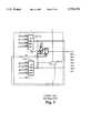
- FIG. 2ashows one embodiment of the invention. Many portions of FIG. 2a correspond to those in FIG. 1a and are given the same labels.
- Multiplexer FX controlled by memory cell Mis provided. Multiplexer FX receives the output signal from LUT G and the inverted output signal from LUT F. The output of Multiplexer FX is provided to multiplexer F5. If memory cell M carries a logic 1, the LUT G output signal is provided to multiplexer F5 and multiplexer F5 functions as in FIG. 1a. If memory cell M carries logic 0, then multiplexer F5 provides a choice of the inverted or noninverted output signal from LUT F as controlled by the signal on line BY.
- the output signal from multiplexer F5is the XOR function of the BY signal and the LUT F output signal.
- the inverted output signal from LUT Fwhich is represented by the bubble at the 0 input of multiplexer FX, is always available because the output signal is buffered through two inverters, not shown in FIG. 2a, and the inverted value is simply taken from the first inverter.
- FIG. 3shows the two inverters I1 and I2 placed in series at the output of lookup table LUT F.
- the output signal from inverter I1drives the 0 input terminal of multiplexer FX.
- the output signal from inverter I2drives the 0 input terminal of multiplexer F5.
- a fundamental advantage of the structure of FIG. 2ais that when multiplexers FX and F5 are used as an XOR gate, lookup table LUT G is available for other functions and thus the chip resources required for the arithmetic function are reduced.
- FIG. 2bshows the structure of FIG. 2a implemented as one bit of an adder (the function shown in FIG. 1b). Portions of the structure not used for the adder function are shown in faint lines and portions which implement the adder are shown in heavy lines.
- the carry-in signalis applied to line BY and thus controls multiplexer F5.
- the output of LUT Fis the half sum ai ⁇ bi and the output of multiplexer F5 is the full sum ai ⁇ bi ⁇ carry-in.
- the circuit of FIG. 4aalso generates the carry-out signal to be used as carry-in for the next bit.
- Lookup table LUT Fperforms the calculation a1b0 ⁇ a0b1.
- Lookup table LUT Gperforms the calculation a0b1. This signal is routed through the FPGA general interconnect structure to the BX input terminal, and is used to generate the carry-out signal sent to the next more significant bit.
- the inventive structureallows the calculation to be done in two lookup tables. By contrast, with the structure of FIG. 1a, the calculation would require an extra lookup table.
- FIG. 4aThe type of equation generated in FIG. 4a is used repeatedly in a multiplier.
- FIG. 4bshows generation of r 3 .
- the steps of Table Iare shown in three tables, Tables II through IV, which correspond to calculations performed in FIG. 4b.
- Logic block CLB1makes the calculation shown in Table II.
- the signals a2, b1, a3, and b0are applied to terminals F3 through F0 of lookup table LUT F, which is programmed to make the calculation a2b1 ⁇ a3b0.
- Lookup table LUT G of CLB1makes the calculation a2b1 and this result is applied through interconnect lines to terminal BX of logic block CLB1.
- the carry-in terminal of logic block CLB1receives the carry-out signal COUTr2-1, which is generated in another logic block not shown.
- logic block CLB1generates on its F5 output terminal the function r3-1, which can be seen in Table II to be a3b0 ⁇ a2b1, and generates on its carry-out terminal the r3-1 carry-out signal COUTr3-1.
- logic block CLB2makes the calculation shown in Table III.
- the signals a1, b2, a0, and b3are applied to the F3 through F0 input terminals of lookup table LUTF and lookup table LUT F is programmed to generated the function alb2 ⁇ a0b3.
- the carry-in signal from r1-1is always 0, as can be understood from Table III since a0b2 is always added to 0 and thus produces a logical 0 carry-out value.
- logic block CLB2generates in its F5 output terminal the function r3-2, which can be seen in Table III to be a1b2 ⁇ a0b3.
- Logic block CLB2generates on its carry-out terminal the r3-1 carry-out signal COUTr3-2.
- Results from CLB1 and CLB2are used in CLB3 to generate the final value r3.
- Lookup table LUT Gis not used and is thus available for other functions.
- the inventionsaves one lookup table in generating bit r1 and three lookup tables in generating bit r3.
- FIG. 5shows the structure of FIG. 2 configured to implement an 8-bit wide parity tree.
- a parity sum of eight data bits d0 through d7is generated by applying the eight data bits to the input terminals shown.
- General interconnect of the FPGA(not shown) is used to route the output signal from LUT G (the parity sum d0 ⁇ d1 ⁇ d2 ⁇ d3) to terminal BY for controlling multiplexer F5.
- Multiplexer F5receives inverted and noninverted parity sums d4 ⁇ d5 ⁇ d6 ⁇ d7.
- the output signal P of multiplexer F5is the parity sum of the eight data bits d0 ⁇ d1 ⁇ d2 ⁇ d3 ⁇ d4 ⁇ d5 ⁇ d6 ⁇ d7.
- FIG. 6shows the structure of FIG. 2 used to implement one bit of a parallel loadable counter with a set/reset signal.
- the reset signalis applied to terminal G1. If reset is logical 1, then G1 is logical 0 and the output of lookup table LUT G is logical 0 regardless of other input signals. If reset is logical 0 then other signals control the output value.
- the set/reset signalis globally controlled and thus resets all bits in the counter.
- the Load/Count signal on G3determines whether the counter will load a new value into the counter or will continue with a count. If Load/Count is logical 0, a new value is loaded from terminal G2 and if Load/Count is logical 1 then the SUM1 value at terminal GO is stored in flip flop 61. For incrementing the register by 1, logical 0 is applied to each line BX for each bit in the counter, and logical 1 is applied to the carry-in terminal of the least significant bit. Each other bit of the counter receives its carry-in signal from the carry-out of the previous bit. When the counter of FIG. 6 is in its counting mode, SUM1 is passed through LUT G to D flip flop 61.
- the SUM1 valueWhen Load/Count is high, the SUM1 value is always one clock tick ahead of the COUNT value it increments.
- Lookup table LUT Fis programmed to act as a feed through for the COUNT signal. This applies the COUNT value to the CMUX control terminal and to the XOR gate formed by multiplexers FX and F5.
- the Carry-in signalis applied to the control terminal of the F5 multiplexer, performing the XOR function.
- the SUM1 signalis the sum of the Carry-in and COUNT values.
- multiplexer FXWithout the extra multiplexer FX to complete the XOR function it would not be possible to separately calculate the sum and also provide both the set/reset and the load function within one logic block. Thus many useful benefits result from the addition of multiplexer FX.
Landscapes
- Physics & Mathematics (AREA)
- General Physics & Mathematics (AREA)
- Engineering & Computer Science (AREA)
- Computational Mathematics (AREA)
- Mathematical Analysis (AREA)
- Pure & Applied Mathematics (AREA)
- Theoretical Computer Science (AREA)
- Mathematical Optimization (AREA)
- Computing Systems (AREA)
- General Engineering & Computer Science (AREA)
- Logic Circuits (AREA)
Abstract
Description
The invention relates to field programmable integrated circuit devices or FPGAs, particularly to logic blocks which make up the FPGAs.
Since the first FPGA was invented in 1984, variations on the basic FPGA have been devised to let the FPGA do specialized functions more efficiently. Special interconnection lines allow adjacent logic blocks to be connected without taking up general interconnection lines. Hardware allowing the carry function to be fast with respect to addition has been placed between adjacent logic blocks. Thus, prior art FPGAs can implement adders and other arithmetic functions at high speed. However, typically, a prior art structure having lookup tables and a carry chain with multiplexers will require two lookup tables to implement one bit of an adder, one pair of lookup tables and one carry multiplexer being used for each digit of the sum. Two 4-input lookup tables are needed because the full adder requires both the sum (the XOR of the two input signals and the carry-in signal from the next lower order bit) and the carry-propagate signal (the XOR of the two input signals alone) for controlling the carry chain. One 4-input lookup table can implement either the sum or the carry-propagate but not both. For other arithmetic functions such as multiply, the number of lookup tables is greater than two per bit.
FIG. 1a shows part of a prior art logic block that includes a carry chain. A typical logic block in FPGA products available from Xilinx, Inc. includes more structures than those shown in FIG. 1a. Such structures are shown at pages 2-9 through 2-13 of the Xilinx 1994 Data Book available from Xilinx, Inc., 2100 Logic Drive, San Jose, Calif. 95124. Such additional structures are also shown by Hsieh et al in FIG. 9 of U.S. Pat. No. 5,267,187 (docket M-1230). As shown in FIG. 1a, the logic block includes two lookup tables LUT F and LUT G, a carry multiplexer CMUX, and a multiplexer F5 for using the two lookup tables to implement one five-input function.
FIG. 1b shows the structure of FIG. 1a configured to implement one bit of an adder. We see in FIG. 1b that the prior art structure of FIG. 1a requires two lookup tables LUT F and LUT G to process one bit of an adder. When the structure of FIG. 1a is configured as in FIG. 1b to implement addition, a carry-in signal from a lower order bit is applied to the 1 input terminal of carry multiplexer CMUX and to an input terminal G1 of lookup table LUT G. The two input signals ai and bi are applied to two input terminals F0 and F1 of lookup table LUT F and to two input terminals G2 and G3 of LUT G. Either of the input signals ai or bi (shown here as ai) is applied to the 0 input terminal of carry-multiplexer CMUX. Lookup table LUT F is configured to generate the XOR function (ai ⊕ bi) of the signals on the F0 and F1 input terminals. Lookup table LUT G is configured to generate the XOR function (ai ⊕ bi ⊕ carry-in) of G1, G2, and G3. The carry-in signal may be routed through general interconnect to carry-in terminal G1, or as shown in FIG. 9 of U.S. Pat. No. 5,267,187 the carry-in signal may be directly routed to and selected by a multiplexer which receives this signal as an input. Thus lookup table LUT F generates the carry propagate signal for controlling multiplexer CMUX. Lookup table LUT G generates the sum.
The present invention adds a small number of additional circuit elements to the prior art structures. The novel circuit allows a logic block to implement an additional XOR function as well as several other useful functions. With the invention, one bit of an adder can be formed using only a single lookup table, a carry multiplexer, and two multiplexers provided as part of the logic block. Multipliers, adders, counters, and loadable synchronous set-reset counters are all conveniently implemented with the invention. Even though the addition of a multiplexer increases the chip area slightly, the total chip resources required to implement many functions are less than when implemented in prior art structures.
FIG. 1a shows a prior art structure for implementing arithmetic functions requiring carry.
FIG. 1b shows the structure of FIG. 1a configured for implementing one bit of an adder.
FIG. 2a shows a structure according to the invention for implementing arithmetic functions requiring carry.
FIG. 2b shows the structure of FIG. 2a configured to implement an adder.
FIG. 3 shows how the inverted input signal to multiplexer FX is derived.
FIGS. 4a and 4b show logic blocks of the invention configured to generate two bits of a multiplier.
FIG. 5 shows a logic block of the invention configured to generate an 8-bit parity sum.
FIG. 6 shows the logic block of the invention configured to generate one bit of a parallel loadable set/reset counter.
FIG. 2a shows one embodiment of the invention. Many portions of FIG. 2a correspond to those in FIG. 1a and are given the same labels. In addition, Multiplexer FX controlled by memory cell M is provided. Multiplexer FX receives the output signal from LUT G and the inverted output signal from LUT F. The output of Multiplexer FX is provided to multiplexer F5. If memory cell M carries alogic 1, the LUT G output signal is provided to multiplexer F5 and multiplexer F5 functions as in FIG. 1a. If memory cell M carrieslogic 0, then multiplexer F5 provides a choice of the inverted or noninverted output signal from LUT F as controlled by the signal on line BY. Thus the output signal from multiplexer F5 is the XOR function of the BY signal and the LUT F output signal. The inverted output signal from LUT F, which is represented by the bubble at the 0 input of multiplexer FX, is always available because the output signal is buffered through two inverters, not shown in FIG. 2a, and the inverted value is simply taken from the first inverter. FIG. 3 shows the two inverters I1 and I2 placed in series at the output of lookup table LUT F. The output signal from inverter I1 drives the 0 input terminal of multiplexer FX. The output signal from inverter I2 drives the 0 input terminal of multiplexer F5.
A fundamental advantage of the structure of FIG. 2a is that when multiplexers FX and F5 are used as an XOR gate, lookup table LUT G is available for other functions and thus the chip resources required for the arithmetic function are reduced.
Adder
FIG. 2b shows the structure of FIG. 2a implemented as one bit of an adder (the function shown in FIG. 1b). Portions of the structure not used for the adder function are shown in faint lines and portions which implement the adder are shown in heavy lines. In FIG. 2b, the carry-in signal is applied to line BY and thus controls multiplexer F5. Thus the output of LUT F is the half sum ai ⊕ bi and the output of multiplexer F5 is the full sum ai ⊕ bi ⊕ carry-in.
Multiplier
Consider a 4-bit by 4-bit multiplier for calculating a3 a2 a1 a0 times b3 b2 b1 b0. The calculation steps are shown in Table I below:
TABLE I ______________________________________ a.sub.3 a.sub.2 a.sub.1 a.sub.0 times b.sub.3 b.sub.2 b.sub.1 b.sub.0 a.sub.3 b.sub.0 a.sub.2 b.sub.0 a.sub.1 b.sub.0 a.sub.0 b.sub.0 + a.sub.3 b.sub.1 a.sub.2 b.sub.1 a.sub.1 b.sub.1 a.sub.0 b.sub.1 0 + a.sub.3 b.sub.2 a.sub.2 b.sub.2 a.sub.1 b.sub.2 a.sub.0 b.sub.2 0 0 + a.sub.3 b.sub.3 a.sub.2 b.sub.3 a.sub.1 b.sub.3 a.sub.0 b.sub.3 0 0 0 r.sub.7 r.sub.6 r.sub.5 r.sub.4 r.sub.3 r.sub.2 r.sub.1 r.sub.0 ______________________________________
The configuration of FIG. 4a generates the r1 bit of the multiplication shown in Table I: r1=alb0+a0b1. The circuit of FIG. 4a also generates the carry-out signal to be used as carry-in for the next bit. Lookup table LUT F performs the calculation a1b0 ⊕ a0b1. Lookup table LUT G performs the calculation a0b1. This signal is routed through the FPGA general interconnect structure to the BX input terminal, and is used to generate the carry-out signal sent to the next more significant bit. The inventive structure allows the calculation to be done in two lookup tables. By contrast, with the structure of FIG. 1a, the calculation would require an extra lookup table.
The type of equation generated in FIG. 4a is used repeatedly in a multiplier. FIG. 4b shows generation of r3. In order to understand generation of multiplier bit r3, the steps of Table I are shown in three tables, Tables II through IV, which correspond to calculations performed in FIG. 4b.
TABLE II ______________________________________ a.sub.3 b.sub.0 a.sub.2 b.sub.0 a.sub.1 b.sub.0 a.sub.0 b.sub.0 + a.sub.3 b.sub.1 a.sub.2 b.sub.1 a.sub.1 b.sub.1 a.sub.0 b.sub.1 0 r.sub.5 - 1 r.sub.4 - 1 r.sub.3 - 1 r.sub.2 - 1 r.sub.1 - 1 r.sub.0 - 1 ______________________________________
TABLE III ______________________________________ a.sub.3 b.sub.2 a.sub.2 b.sub.2 a.sub.1 b.sub.2 a.sub.0 b.sub.2 0 0 + a.sub.3 b.sub.3 a.sub.2 b.sub.3 a.sub.1 b.sub.3 a.sub.0 b.sub.3 0 0 0 r.sub.7 - 2 r.sub.6 - 2 r.sub.5 - 2 r.sub.4 - 2 r.sub.3 - 2 r.sub.2 - 2 r.sub.1 - 2 r.sub.0 - 2 ______________________________________
TABLE IV ______________________________________ r.sub.5 - 1 r.sub.4 - 1 r.sub.3 - 1 r.sub.2 - 1 r.sub.1 - 1 r.sub.0 - 1 r.sub.7 - 2 r.sub.6 - 2 r.sub.5 - 2 r.sub.4 - 2 r.sub.3 - 2 r.sub.2 - 2 r.sub.1 - 2 r.sub.0 - 2 r.sub.7 r.sub.6 r.sub.5 r.sub.4 r.sub.3 r.sub.2 r.sub.1 r.sub.0 ______________________________________
Logic block CLB1 makes the calculation shown in Table II. The signals a2, b1, a3, and b0 are applied to terminals F3 through F0 of lookup table LUT F, which is programmed to make the calculation a2b1 ⊕ a3b0. Lookup table LUT G of CLB1 makes the calculation a2b1 and this result is applied through interconnect lines to terminal BX of logic block CLB1. The carry-in terminal of logic block CLB1 receives the carry-out signal COUTr2-1, which is generated in another logic block not shown. Thus logic block CLB1 generates on its F5 output terminal the function r3-1, which can be seen in Table II to be a3b0 ⊕ a2b1, and generates on its carry-out terminal the r3-1 carry-out signal COUTr3-1.
Similarly, logic block CLB2 makes the calculation shown in Table III. The signals a1, b2, a0, and b3 are applied to the F3 through F0 input terminals of lookup table LUTF and lookup table LUT F is programmed to generated the function alb2 ⊕ a0b3. The carry-in signal from r1-1 is always 0, as can be understood from Table III since a0b2 is always added to 0 and thus produces a logical 0 carry-out value. Thus logic block CLB2 generates in its F5 output terminal the function r3-2, which can be seen in Table III to be a1b2 ⊕ a0b3. Logic block CLB2 generates on its carry-out terminal the r3-1 carry-out signal COUTr3-2.
Results from CLB1 and CLB2 are used in CLB3 to generate the final value r3. Lookup table LUT G is not used and is thus available for other functions. The signals r3-1 and r3-2 are applied to terminals F3 and F2 of lookup table LUT F, and lookup table LUT F is programmed to generate the function r3-1 ⊕ r3-2, which is combined in multiplexers M and F5 with carry-in signal COUTr2 to generate the final output function r3=r3-1 ⊕ r3-2⊕COUTr2.
Thus the invention saves one lookup table in generating bit r1 and three lookup tables in generating bit r3. The larger the arithmetic function, the greater the density increase provided by the multiplexer combination of the invention.
Parity Tree
FIG. 5 shows the structure of FIG. 2 configured to implement an 8-bit wide parity tree. A parity sum of eight data bits d0 through d7 is generated by applying the eight data bits to the input terminals shown. General interconnect of the FPGA (not shown) is used to route the output signal from LUT G (the parity sum d0⊕d1⊕d2⊕d3) to terminal BY for controlling multiplexer F5. Multiplexer F5 receives inverted and noninverted parity sums d4⊕d5⊕d6⊕d7. Thus the output signal P of multiplexer F5 is the parity sum of the eight data bits d0⊕d1⊕d2⊕d3⊕d4⊕d5⊕d6⊕d7.
Complex Counter
FIG. 6 shows the structure of FIG. 2 used to implement one bit of a parallel loadable counter with a set/reset signal. Lookup table LUT G is programmed with the truth table G=(G3.G2+G3.G0).G1. This truth table causes G1 to be a reset signal. (The truth table G=(G3.G2+G3.G0)+G1 would cause G1 to serve as a set signal.) The reset signal is applied to terminal G1. If reset is logical 1, then G1 is logical 0 and the output of lookup table LUT G is logical 0 regardless of other input signals. If reset is logical 0 then other signals control the output value.
Typically the set/reset signal is globally controlled and thus resets all bits in the counter.
The Load/Count signal on G3 determines whether the counter will load a new value into the counter or will continue with a count. If Load/Count is logical 0, a new value is loaded from terminal G2 and if Load/Count is logical 1 then the SUM1 value at terminal GO is stored inflip flop 61. For incrementing the register by 1, logical 0 is applied to each line BX for each bit in the counter, and logical 1 is applied to the carry-in terminal of the least significant bit. Each other bit of the counter receives its carry-in signal from the carry-out of the previous bit. When the counter of FIG. 6 is in its counting mode, SUM1 is passed through LUT G toD flip flop 61. When Load/Count is high, the SUM1 value is always one clock tick ahead of the COUNT value it increments. Lookup table LUT F is programmed to act as a feed through for the COUNT signal. This applies the COUNT value to the CMUX control terminal and to the XOR gate formed by multiplexers FX and F5. The Carry-in signal is applied to the control terminal of the F5 multiplexer, performing the XOR function. Thus the SUM1 signal is the sum of the Carry-in and COUNT values.
Without the extra multiplexer FX to complete the XOR function it would not be possible to separately calculate the sum and also provide both the set/reset and the load function within one logic block. Thus many useful benefits result from the addition of multiplexer FX.
In light of the above description, other embodiments of the invention will become obvious to those skilled in the art. For example, if an FPGA designer does not want to offer the function of five input variables, the two multiplexers can be replaced by an XOR gate.
Claims (3)
1. A field programmable gate array (FPGA) logic block structure comprising:
a first multiplexer having at least two data inputs and at least one control input;
a second multiplexer having at least two data inputs and at least one control input, said second multiplexer providing a first data input to said first multiplexer;
a first lookup table having a plurality of inputs, said first lookup table providing true and complement output signals, one as a second data input to said first multiplexer and one as a first data input to said second multiplexer;
a second lookup table having a plurality of inputs, said second lookup table providing a second data input to said second multiplexer; and
a plurality of lines accessible from a general interconnect structure of an FPGA, one of said lines providing a control input to said first multiplexer, and other of said lines providing said inputs to said first and second lookup tables.
2. An FPGA logic block structure as in claim 1 further comprising:
a carry multiplexer having at least two data inputs and at least one control input, said carry multiplexer receiving as a first data input a carry-in signal from an upstream carry multiplexer and providing a carryout signal to a location external to said logic block; one of said lines providing a second data input to said carry multiplexer, said carry multiplexer receiving as a control input one of said true and complement output signals.
3. An FPGA logic block structure as in claim 2 wherein said location external to said logic block is a downstream multiplexer.
Priority Applications (1)
| Application Number | Priority Date | Filing Date | Title |
|---|---|---|---|
| US08/664,628US5724276A (en) | 1996-06-17 | 1996-06-17 | Logic block structure optimized for sum generation |
Applications Claiming Priority (1)
| Application Number | Priority Date | Filing Date | Title |
|---|---|---|---|
| US08/664,628US5724276A (en) | 1996-06-17 | 1996-06-17 | Logic block structure optimized for sum generation |
Publications (1)
| Publication Number | Publication Date |
|---|---|
| US5724276Atrue US5724276A (en) | 1998-03-03 |
Family
ID=24666768
Family Applications (1)
| Application Number | Title | Priority Date | Filing Date |
|---|---|---|---|
| US08/664,628Expired - LifetimeUS5724276A (en) | 1996-06-17 | 1996-06-17 | Logic block structure optimized for sum generation |
Country Status (1)
| Country | Link |
|---|---|
| US (1) | US5724276A (en) |
Cited By (67)
| Publication number | Priority date | Publication date | Assignee | Title |
|---|---|---|---|---|
| US5889411A (en)* | 1997-02-26 | 1999-03-30 | Xilinx, Inc. | FPGA having logic element carry chains capable of generating wide XOR functions |
| US5907248A (en)* | 1997-02-26 | 1999-05-25 | Xilinx, Inc. | FPGA interconnect structure with high-speed high fanout capability |
| US5920202A (en)* | 1997-02-26 | 1999-07-06 | Xilinx, Inc. | Configurable logic element with ability to evaluate five and six input functions |
| US5942913A (en)* | 1997-03-20 | 1999-08-24 | Xilinx, Inc. | FPGA repeatable interconnect structure with bidirectional and unidirectional interconnect lines |
| US5963050A (en)* | 1997-02-26 | 1999-10-05 | Xilinx, Inc. | Configurable logic element with fast feedback paths |
| US6118300A (en)* | 1998-11-24 | 2000-09-12 | Xilinx, Inc. | Method for implementing large multiplexers with FPGA lookup tables |
| US6201410B1 (en) | 1997-02-26 | 2001-03-13 | Xilinx, Inc. | Wide logic gate implemented in an FPGA configurable logic element |
| US6204689B1 (en) | 1997-02-26 | 2001-03-20 | Xilinx, Inc. | Input/output interconnect circuit for FPGAs |
| US6289400B1 (en)* | 1998-04-15 | 2001-09-11 | Infineon Technologies Ag | Electrical control device with configurable control modules |
| US6288570B1 (en)* | 1993-09-02 | 2001-09-11 | Xilinx, Inc. | Logic structure and circuit for fast carry |
| US6362650B1 (en)* | 2000-05-18 | 2002-03-26 | Xilinx, Inc. | Method and apparatus for incorporating a multiplier into an FPGA |
| US6397241B1 (en)* | 1998-12-18 | 2002-05-28 | Motorola, Inc. | Multiplier cell and method of computing |
| US6427156B1 (en)* | 1997-01-21 | 2002-07-30 | Xilinx, Inc. | Configurable logic block with AND gate for efficient multiplication in FPGAS |
| US20020116426A1 (en)* | 2001-02-15 | 2002-08-22 | Stmicroelectronics Ltd. | Look-up table apparatus to perform two-bit arithmetic operation including carry generation |
| US6466052B1 (en)* | 2001-05-15 | 2002-10-15 | Xilinx, Inc. | Implementing wide multiplexers in an FPGA using a horizontal chain structure |
| US20020169812A1 (en)* | 2001-03-31 | 2002-11-14 | Orchard John T. | Architecture and related methods for efficiently performing complex arithmetic |
| US6505337B1 (en) | 1998-11-24 | 2003-01-07 | Xilinx, Inc. | Method for implementing large multiplexers with FPGA lookup tables |
| US6516332B1 (en)* | 1996-09-02 | 2003-02-04 | Siemens Plc | Floating point number data processing means |
| US6724810B1 (en) | 2000-11-17 | 2004-04-20 | Xilinx, Inc. | Method and apparatus for de-spreading spread spectrum signals |
| US20040145942A1 (en)* | 2001-05-16 | 2004-07-29 | Katarzyna Leijten-Nowak | Reconfigurable logic device |
| US20040155676A1 (en)* | 2003-02-11 | 2004-08-12 | Sinan Kaptanoglu | Fracturable incomplete look up table for area efficient logic elements |
| US6798240B1 (en) | 2003-01-24 | 2004-09-28 | Altera Corporation | Logic circuitry with shared lookup table |
| US6847228B1 (en)* | 2002-11-19 | 2005-01-25 | Xilinx, Inc. | Carry logic design having simplified timing modeling for a field programmable gate array |
| US20050144215A1 (en)* | 2003-12-29 | 2005-06-30 | Xilinx, Inc. | Applications of cascading DSP slices |
| US20050144211A1 (en)* | 2003-12-29 | 2005-06-30 | Xilinx, Inc. | Programmable logic device with pipelined DSP slices |
| US20050144213A1 (en)* | 2003-12-29 | 2005-06-30 | Xilinx, Inc. | Mathematical circuit with dynamic rounding |
| US20050144210A1 (en)* | 2003-12-29 | 2005-06-30 | Xilinx, Inc. | Programmable logic device with dynamic DSP architecture |
| US20050144212A1 (en)* | 2003-12-29 | 2005-06-30 | Xilinx, Inc. | Programmable logic device with cascading DSP slices |
| US20050144216A1 (en)* | 2003-12-29 | 2005-06-30 | Xilinx, Inc. | Arithmetic circuit with multiplexed addend inputs |
| US6943580B2 (en) | 2003-02-10 | 2005-09-13 | Altera Corporation | Fracturable lookup table and logic element |
| US20050289211A1 (en)* | 2004-06-17 | 2005-12-29 | Stmicroelectronics Pvt.Ltd. | One bit full adder with sum and carry outputs capable of independent functionalities |
| US20060059222A1 (en)* | 2004-08-03 | 2006-03-16 | Stmicroelectronics Pvt. Ltd. | Logic entity with two outputs for efficient adder and other macro implementations |
| US7061268B1 (en) | 2004-03-15 | 2006-06-13 | Altera Corporation | Initializing a carry chain in a programmable logic device |
| US20060190516A1 (en)* | 2003-12-29 | 2006-08-24 | Xilinx, Inc. | Digital signal processing element having an arithmetic logic unit |
| US20060195496A1 (en)* | 2003-12-29 | 2006-08-31 | Xilinx, Inc. | Digital signal processing circuit having a pattern detector circuit |
| US20060212499A1 (en)* | 2003-12-29 | 2006-09-21 | Xilinx, Inc. | Digital signal processing block having a wide multiplexer |
| US20060230095A1 (en)* | 2003-12-29 | 2006-10-12 | Xilinx, Inc. | Digital signal processing circuit having a pre-adder circuit |
| US20060230096A1 (en)* | 2003-12-29 | 2006-10-12 | Xilinx, Inc. | Digital signal processing circuit having an adder circuit with carry-outs |
| US20060230094A1 (en)* | 2003-12-29 | 2006-10-12 | Xilinx, Inc. | Digital signal processing circuit having input register blocks |
| US20060230092A1 (en)* | 2003-12-29 | 2006-10-12 | Xilinx, Inc. | Architectural floorplan for a digital signal processing circuit |
| US20060230093A1 (en)* | 2003-12-29 | 2006-10-12 | Xilinx, Inc. | Digital signal processing circuit having a pattern detector circuit for convergent rounding |
| US20060288070A1 (en)* | 2003-12-29 | 2006-12-21 | Xilinx, Inc. | Digital signal processing circuit having a pattern circuit for determining termination conditions |
| US20060288069A1 (en)* | 2003-12-29 | 2006-12-21 | Xilinx, Inc. | Digital signal processing circuit having a SIMD circuit |
| US7167021B1 (en) | 2003-11-24 | 2007-01-23 | Altera Corporation | Logic device logic modules having improved arithmetic circuitry |
| US7185035B1 (en) | 2003-10-23 | 2007-02-27 | Altera Corporation | Arithmetic structures for programmable logic devices |
| US7205791B1 (en) | 2004-03-12 | 2007-04-17 | Altera Corporation | Bypass-able carry chain in a programmable logic device |
| US20070230336A1 (en)* | 2006-03-10 | 2007-10-04 | Fujitsu Limited | Reconfigurable circuit |
| US7558812B1 (en)* | 2003-11-26 | 2009-07-07 | Altera Corporation | Structures for LUT-based arithmetic in PLDs |
| US7565388B1 (en) | 2003-11-21 | 2009-07-21 | Altera Corporation | Logic cell supporting addition of three binary words |
| WO2009100564A1 (en)* | 2008-01-30 | 2009-08-20 | Agate Logic (Beijing), Inc. | An integrated circuit with improved logic cells |
| US20100013517A1 (en)* | 2006-06-28 | 2010-01-21 | Rajit Manohar | Reconfigurable logic fabrics for integrated circuits and systems and methods for configuring reconfigurable logic fabrics |
| US7663400B1 (en) | 2007-12-21 | 2010-02-16 | Actel Corporation | Flexible carry scheme for field programmable gate arrays |
| US7671625B1 (en) | 2004-03-25 | 2010-03-02 | Altera Corporation | Omnibus logic element |
| US20100191786A1 (en)* | 2009-01-27 | 2010-07-29 | Xilinx, Inc. | Digital signal processing block with preadder stage |
| US20100192118A1 (en)* | 2009-01-27 | 2010-07-29 | Xilinx, Inc. | Method of and circuit for implementing a filter in an integrated circuit |
| US7772879B1 (en) | 2007-04-11 | 2010-08-10 | Actel Corporation | Logic module including versatile adder for FPGA |
| US7800401B1 (en) | 2003-02-10 | 2010-09-21 | Altera Corporation | Fracturable lookup table and logic element |
| US7840630B2 (en) | 2003-12-29 | 2010-11-23 | Xilinx, Inc. | Arithmetic logic unit circuit |
| US7900078B1 (en) | 2009-09-14 | 2011-03-01 | Achronix Semiconductor Corporation | Asynchronous conversion circuitry apparatus, systems, and methods |
| US20110058570A1 (en)* | 2009-09-10 | 2011-03-10 | Virantha Ekanayake | Programmable crossbar structures in asynchronous systems |
| US8244791B1 (en) | 2008-01-30 | 2012-08-14 | Actel Corporation | Fast carry lookahead circuits |
| US8352532B1 (en)* | 2009-08-20 | 2013-01-08 | Xilinx, Inc. | Circuit structure for multiplying numbers using look-up tables and adders |
| EP2550593A4 (en)* | 2010-03-25 | 2014-03-05 | Altera Corp | CONSULTING TABLE STRUCTURE SUPPORTING QUATERNARY ADDITIONERS |
| US10936286B2 (en)* | 2018-11-13 | 2021-03-02 | Microsemi Soc Corp. | FPGA logic cell with improved support for counters |
| CN113872608A (en)* | 2021-12-01 | 2021-12-31 | 中国人民解放军海军工程大学 | A Wallace Tree Compressor Based on Xilinx FPGA Primitives |
| US20220376693A1 (en)* | 2021-05-21 | 2022-11-24 | Microchip Technology Inc. | Logic cell for programmable gate array |
| US12223322B2 (en) | 2021-10-07 | 2025-02-11 | Microchip Technology Inc. | Embedded processor supporting fixed-function kernels |
Citations (4)
| Publication number | Priority date | Publication date | Assignee | Title |
|---|---|---|---|---|
| US5267187A (en)* | 1990-05-10 | 1993-11-30 | Xilinx Inc | Logic structure and circuit for fast carry |
| US5436574A (en)* | 1993-11-12 | 1995-07-25 | Altera Corporation | Universal logic module with arithmetic capabilities |
| US5481206A (en)* | 1993-09-02 | 1996-01-02 | Xilinx, Inc. | Circuit for fast carry and logic |
| US5481486A (en)* | 1992-05-08 | 1996-01-02 | Altera Corporation | Look up table implementation of fast carry arithmetic and exclusive-OR operations |
- 1996
- 1996-06-17USUS08/664,628patent/US5724276A/ennot_activeExpired - Lifetime
Patent Citations (4)
| Publication number | Priority date | Publication date | Assignee | Title |
|---|---|---|---|---|
| US5267187A (en)* | 1990-05-10 | 1993-11-30 | Xilinx Inc | Logic structure and circuit for fast carry |
| US5481486A (en)* | 1992-05-08 | 1996-01-02 | Altera Corporation | Look up table implementation of fast carry arithmetic and exclusive-OR operations |
| US5481206A (en)* | 1993-09-02 | 1996-01-02 | Xilinx, Inc. | Circuit for fast carry and logic |
| US5436574A (en)* | 1993-11-12 | 1995-07-25 | Altera Corporation | Universal logic module with arithmetic capabilities |
Non-Patent Citations (2)
| Title |
|---|
| "The Programmable Logic Data Book", 1994, pp. 2-9 through 2-13, available from Xilinx Inc., 2100 Logic Drive, San Jose, CA 95124. |
| The Programmable Logic Data Book , 1994, pp. 2 9 through 2 13, available from Xilinx Inc., 2100 Logic Drive, San Jose, CA 95124.* |
Cited By (133)
| Publication number | Priority date | Publication date | Assignee | Title |
|---|---|---|---|---|
| US6288570B1 (en)* | 1993-09-02 | 2001-09-11 | Xilinx, Inc. | Logic structure and circuit for fast carry |
| US6516332B1 (en)* | 1996-09-02 | 2003-02-04 | Siemens Plc | Floating point number data processing means |
| US6708191B2 (en) | 1997-01-21 | 2004-03-16 | Xilinx, Inc. | Configurable logic block with and gate for efficient multiplication in FPGAS |
| US6427156B1 (en)* | 1997-01-21 | 2002-07-30 | Xilinx, Inc. | Configurable logic block with AND gate for efficient multiplication in FPGAS |
| US6124731A (en)* | 1997-02-26 | 2000-09-26 | Xilinx, Inc. | Configurable logic element with ability to evaluate wide logic functions |
| US6051992A (en)* | 1997-02-26 | 2000-04-18 | Xilinx, Inc. | Configurable logic element with ability to evaluate five and six input functions |
| US6107827A (en)* | 1997-02-26 | 2000-08-22 | Xilinx, Inc. | FPGA CLE with two independent carry chains |
| US6448808B2 (en) | 1997-02-26 | 2002-09-10 | Xilinx, Inc. | Interconnect structure for a programmable logic device |
| US5889411A (en)* | 1997-02-26 | 1999-03-30 | Xilinx, Inc. | FPGA having logic element carry chains capable of generating wide XOR functions |
| US5920202A (en)* | 1997-02-26 | 1999-07-06 | Xilinx, Inc. | Configurable logic element with ability to evaluate five and six input functions |
| US6201410B1 (en) | 1997-02-26 | 2001-03-13 | Xilinx, Inc. | Wide logic gate implemented in an FPGA configurable logic element |
| US6204690B1 (en) | 1997-02-26 | 2001-03-20 | Xilinx, Inc. | FPGA architecture with offset interconnect lines |
| US6204689B1 (en) | 1997-02-26 | 2001-03-20 | Xilinx, Inc. | Input/output interconnect circuit for FPGAs |
| US5963050A (en)* | 1997-02-26 | 1999-10-05 | Xilinx, Inc. | Configurable logic element with fast feedback paths |
| US6292022B2 (en) | 1997-02-26 | 2001-09-18 | Xilinx, Inc. | Interconnect structure for a programmable logic device |
| US5907248A (en)* | 1997-02-26 | 1999-05-25 | Xilinx, Inc. | FPGA interconnect structure with high-speed high fanout capability |
| US5942913A (en)* | 1997-03-20 | 1999-08-24 | Xilinx, Inc. | FPGA repeatable interconnect structure with bidirectional and unidirectional interconnect lines |
| US6289400B1 (en)* | 1998-04-15 | 2001-09-11 | Infineon Technologies Ag | Electrical control device with configurable control modules |
| US6505337B1 (en) | 1998-11-24 | 2003-01-07 | Xilinx, Inc. | Method for implementing large multiplexers with FPGA lookup tables |
| US6191610B1 (en) | 1998-11-24 | 2001-02-20 | Xilinx, Inc. | Method for implementing large multiplexers with FPGA lookup tables |
| US6118300A (en)* | 1998-11-24 | 2000-09-12 | Xilinx, Inc. | Method for implementing large multiplexers with FPGA lookup tables |
| US6671709B2 (en) | 1998-12-18 | 2003-12-30 | Motorola, Inc. | Multiplier cell and method of computing |
| US6397241B1 (en)* | 1998-12-18 | 2002-05-28 | Motorola, Inc. | Multiplier cell and method of computing |
| US6573749B2 (en) | 2000-05-18 | 2003-06-03 | Xilinx, Inc. | Method and apparatus for incorporating a multiplier into an FPGA |
| US6362650B1 (en)* | 2000-05-18 | 2002-03-26 | Xilinx, Inc. | Method and apparatus for incorporating a multiplier into an FPGA |
| US6724810B1 (en) | 2000-11-17 | 2004-04-20 | Xilinx, Inc. | Method and apparatus for de-spreading spread spectrum signals |
| US20020116426A1 (en)* | 2001-02-15 | 2002-08-22 | Stmicroelectronics Ltd. | Look-up table apparatus to perform two-bit arithmetic operation including carry generation |
| US6961741B2 (en)* | 2001-02-15 | 2005-11-01 | Stmicroelectronics Ltd. | Look-up table apparatus to perform two-bit arithmetic operation including carry generation |
| US20020169812A1 (en)* | 2001-03-31 | 2002-11-14 | Orchard John T. | Architecture and related methods for efficiently performing complex arithmetic |
| US7424506B2 (en)* | 2001-03-31 | 2008-09-09 | Durham Logistics Llc | Architecture and related methods for efficiently performing complex arithmetic |
| US6466052B1 (en)* | 2001-05-15 | 2002-10-15 | Xilinx, Inc. | Implementing wide multiplexers in an FPGA using a horizontal chain structure |
| US20040145942A1 (en)* | 2001-05-16 | 2004-07-29 | Katarzyna Leijten-Nowak | Reconfigurable logic device |
| US7251672B2 (en)* | 2001-05-16 | 2007-07-31 | Nxp B.V. | Reconfigurable logic device |
| US6847228B1 (en)* | 2002-11-19 | 2005-01-25 | Xilinx, Inc. | Carry logic design having simplified timing modeling for a field programmable gate array |
| US7317330B2 (en) | 2003-01-24 | 2008-01-08 | Altera Corporation | Logic circuitry with shared lookup table |
| US20050030062A1 (en)* | 2003-01-24 | 2005-02-10 | Bruce Pedersen | Logic circuitry with shared lookup table |
| US6798240B1 (en) | 2003-01-24 | 2004-09-28 | Altera Corporation | Logic circuitry with shared lookup table |
| US7323902B2 (en) | 2003-02-10 | 2008-01-29 | Altera Corporation | Fracturable lookup table and logic element |
| US8217678B1 (en) | 2003-02-10 | 2012-07-10 | Altera Corporation | Fracturable lookup table and logic element |
| US7800401B1 (en) | 2003-02-10 | 2010-09-21 | Altera Corporation | Fracturable lookup table and logic element |
| CN1540865B (en)* | 2003-02-10 | 2010-05-12 | 阿尔特拉公司 | Logic element, programmable logic device, data processing system, and method of manufacturing logic element |
| US20070222477A1 (en)* | 2003-02-10 | 2007-09-27 | Altera Corporation | Fracturable lookup table and logic element |
| US6943580B2 (en) | 2003-02-10 | 2005-09-13 | Altera Corporation | Fracturable lookup table and logic element |
| US7312632B2 (en) | 2003-02-10 | 2007-12-25 | Altera Corporation | Fracturable lookup table and logic element |
| US20060017460A1 (en)* | 2003-02-10 | 2006-01-26 | Altera Corporation | Fracturable lookup table and logic element |
| US20040155676A1 (en)* | 2003-02-11 | 2004-08-12 | Sinan Kaptanoglu | Fracturable incomplete look up table for area efficient logic elements |
| US7030650B1 (en) | 2003-02-11 | 2006-04-18 | Altera Corporation | Fracturable incomplete look up table area efficient logic elements |
| US6888373B2 (en) | 2003-02-11 | 2005-05-03 | Altera Corporation | Fracturable incomplete look up table for area efficient logic elements |
| US7185035B1 (en) | 2003-10-23 | 2007-02-27 | Altera Corporation | Arithmetic structures for programmable logic devices |
| US7565388B1 (en) | 2003-11-21 | 2009-07-21 | Altera Corporation | Logic cell supporting addition of three binary words |
| US7167021B1 (en) | 2003-11-24 | 2007-01-23 | Altera Corporation | Logic device logic modules having improved arithmetic circuitry |
| US7558812B1 (en)* | 2003-11-26 | 2009-07-07 | Altera Corporation | Structures for LUT-based arithmetic in PLDs |
| US9658830B1 (en) | 2003-11-26 | 2017-05-23 | Altera Corporation | Structures for LUT-based arithmetic in PLDs |
| US8788550B1 (en) | 2003-11-26 | 2014-07-22 | Altera Corporation | Structures for LUT-based arithmetic in PLDs |
| US7480690B2 (en) | 2003-12-29 | 2009-01-20 | Xilinx, Inc. | Arithmetic circuit with multiplexed addend inputs |
| US7853632B2 (en) | 2003-12-29 | 2010-12-14 | Xilinx, Inc. | Architectural floorplan for a digital signal processing circuit |
| US20060288070A1 (en)* | 2003-12-29 | 2006-12-21 | Xilinx, Inc. | Digital signal processing circuit having a pattern circuit for determining termination conditions |
| US20060288069A1 (en)* | 2003-12-29 | 2006-12-21 | Xilinx, Inc. | Digital signal processing circuit having a SIMD circuit |
| US20060230092A1 (en)* | 2003-12-29 | 2006-10-12 | Xilinx, Inc. | Architectural floorplan for a digital signal processing circuit |
| US20060230094A1 (en)* | 2003-12-29 | 2006-10-12 | Xilinx, Inc. | Digital signal processing circuit having input register blocks |
| US20050144211A1 (en)* | 2003-12-29 | 2005-06-30 | Xilinx, Inc. | Programmable logic device with pipelined DSP slices |
| US20060230096A1 (en)* | 2003-12-29 | 2006-10-12 | Xilinx, Inc. | Digital signal processing circuit having an adder circuit with carry-outs |
| US20060230095A1 (en)* | 2003-12-29 | 2006-10-12 | Xilinx, Inc. | Digital signal processing circuit having a pre-adder circuit |
| US8495122B2 (en) | 2003-12-29 | 2013-07-23 | Xilinx, Inc. | Programmable device with dynamic DSP architecture |
| US20060212499A1 (en)* | 2003-12-29 | 2006-09-21 | Xilinx, Inc. | Digital signal processing block having a wide multiplexer |
| US20060195496A1 (en)* | 2003-12-29 | 2006-08-31 | Xilinx, Inc. | Digital signal processing circuit having a pattern detector circuit |
| US20060190516A1 (en)* | 2003-12-29 | 2006-08-24 | Xilinx, Inc. | Digital signal processing element having an arithmetic logic unit |
| US7882165B2 (en) | 2003-12-29 | 2011-02-01 | Xilinx, Inc. | Digital signal processing element having an arithmetic logic unit |
| US7467177B2 (en) | 2003-12-29 | 2008-12-16 | Xilinx, Inc. | Mathematical circuit with dynamic rounding |
| US7467175B2 (en) | 2003-12-29 | 2008-12-16 | Xilinx, Inc. | Programmable logic device with pipelined DSP slices |
| US7472155B2 (en) | 2003-12-29 | 2008-12-30 | Xilinx, Inc. | Programmable logic device with cascading DSP slices |
| US7870182B2 (en) | 2003-12-29 | 2011-01-11 | Xilinx Inc. | Digital signal processing circuit having an adder circuit with carry-outs |
| US20050144215A1 (en)* | 2003-12-29 | 2005-06-30 | Xilinx, Inc. | Applications of cascading DSP slices |
| US7865542B2 (en) | 2003-12-29 | 2011-01-04 | Xilinx, Inc. | Digital signal processing block having a wide multiplexer |
| US7860915B2 (en) | 2003-12-29 | 2010-12-28 | Xilinx, Inc. | Digital signal processing circuit having a pattern circuit for determining termination conditions |
| US7567997B2 (en) | 2003-12-29 | 2009-07-28 | Xilinx, Inc. | Applications of cascading DSP slices |
| US20060230093A1 (en)* | 2003-12-29 | 2006-10-12 | Xilinx, Inc. | Digital signal processing circuit having a pattern detector circuit for convergent rounding |
| US7853634B2 (en) | 2003-12-29 | 2010-12-14 | Xilinx, Inc. | Digital signal processing circuit having a SIMD circuit |
| US7853636B2 (en) | 2003-12-29 | 2010-12-14 | Xilinx, Inc. | Digital signal processing circuit having a pattern detector circuit for convergent rounding |
| US20050144216A1 (en)* | 2003-12-29 | 2005-06-30 | Xilinx, Inc. | Arithmetic circuit with multiplexed addend inputs |
| US7849119B2 (en) | 2003-12-29 | 2010-12-07 | Xilinx, Inc. | Digital signal processing circuit having a pattern detector circuit |
| US7844653B2 (en) | 2003-12-29 | 2010-11-30 | Xilinx, Inc. | Digital signal processing circuit having a pre-adder circuit |
| US20050144212A1 (en)* | 2003-12-29 | 2005-06-30 | Xilinx, Inc. | Programmable logic device with cascading DSP slices |
| US7840627B2 (en) | 2003-12-29 | 2010-11-23 | Xilinx, Inc. | Digital signal processing circuit having input register blocks |
| US7840630B2 (en) | 2003-12-29 | 2010-11-23 | Xilinx, Inc. | Arithmetic logic unit circuit |
| US20050144210A1 (en)* | 2003-12-29 | 2005-06-30 | Xilinx, Inc. | Programmable logic device with dynamic DSP architecture |
| US20050144213A1 (en)* | 2003-12-29 | 2005-06-30 | Xilinx, Inc. | Mathematical circuit with dynamic rounding |
| US7205791B1 (en) | 2004-03-12 | 2007-04-17 | Altera Corporation | Bypass-able carry chain in a programmable logic device |
| US7061268B1 (en) | 2004-03-15 | 2006-06-13 | Altera Corporation | Initializing a carry chain in a programmable logic device |
| US8593174B1 (en) | 2004-03-25 | 2013-11-26 | Altera Corporation | Omnibus logic element for packing or fracturing |
| US8878567B1 (en) | 2004-03-25 | 2014-11-04 | Altera Corporation | Omnibus logic element |
| US7911230B1 (en) | 2004-03-25 | 2011-03-22 | Altera Corporation | Omnibus logic element for packing or fracturing |
| US9496875B1 (en) | 2004-03-25 | 2016-11-15 | Altera Corporation | Omnibus logic element |
| US7671625B1 (en) | 2004-03-25 | 2010-03-02 | Altera Corporation | Omnibus logic element |
| US8237465B1 (en)* | 2004-03-25 | 2012-08-07 | Altera Corporation | Omnibus logic element for packing or fracturing |
| US10177766B1 (en)* | 2004-03-25 | 2019-01-08 | Altera Corporation | Omnibus logic element |
| US7475105B2 (en)* | 2004-06-17 | 2009-01-06 | Stmicroelectronics Pvt. Ltd. | One bit full adder with sum and carry outputs capable of independent functionalities |
| US20050289211A1 (en)* | 2004-06-17 | 2005-12-29 | Stmicroelectronics Pvt.Ltd. | One bit full adder with sum and carry outputs capable of independent functionalities |
| US20060059222A1 (en)* | 2004-08-03 | 2006-03-16 | Stmicroelectronics Pvt. Ltd. | Logic entity with two outputs for efficient adder and other macro implementations |
| US7617269B2 (en)* | 2004-08-03 | 2009-11-10 | Stmicroelectronics Pvt. Ltd. | Logic entity with two outputs for efficient adder and other macro implementations |
| US20070230336A1 (en)* | 2006-03-10 | 2007-10-04 | Fujitsu Limited | Reconfigurable circuit |
| US8099540B2 (en)* | 2006-03-10 | 2012-01-17 | Fujitsu Semiconductor Limited | Reconfigurable circuit |
| US8575959B2 (en) | 2006-06-28 | 2013-11-05 | Achronix Semiconductor Corporation | Reconfigurable logic fabrics for integrated circuits and systems and methods for configuring reconfigurable logic fabrics |
| US7880499B2 (en)* | 2006-06-28 | 2011-02-01 | Achronix Semiconductor Corporation | Reconfigurable logic fabrics for integrated circuits and systems and methods for configuring reconfigurable logic fabrics |
| US20100013517A1 (en)* | 2006-06-28 | 2010-01-21 | Rajit Manohar | Reconfigurable logic fabrics for integrated circuits and systems and methods for configuring reconfigurable logic fabrics |
| US8949759B2 (en) | 2006-06-28 | 2015-02-03 | Achronix Semiconductor Corporation | Reconfigurable logic fabrics for integrated circuits and systems and methods for configuring reconfigurable logic fabrics |
| US8125242B2 (en) | 2006-06-28 | 2012-02-28 | Achronix Semiconductor Corporation | Reconfigurable logic fabrics for integrated circuits and systems and methods for configuring reconfigurable logic fabrics |
| US20110169524A1 (en)* | 2006-06-28 | 2011-07-14 | Achronix Semiconductor Corporation. | Reconfigurable logic fabrics for integrated circuits and systems and methods for configuring reconfigurable logic fabrics |
| US8085064B2 (en) | 2007-04-11 | 2011-12-27 | Actel Corporation | Logic module including versatile adder for FPGA |
| US20100271068A1 (en)* | 2007-04-11 | 2010-10-28 | Actel Corporation | Logic module including versatile adder for fpga |
| US7772879B1 (en) | 2007-04-11 | 2010-08-10 | Actel Corporation | Logic module including versatile adder for FPGA |
| US7663400B1 (en) | 2007-12-21 | 2010-02-16 | Actel Corporation | Flexible carry scheme for field programmable gate arrays |
| US20100100864A1 (en)* | 2007-12-21 | 2010-04-22 | Actel Corporation | Flexible carry scheme for field programmable gate arrays |
| US7872497B2 (en) | 2007-12-21 | 2011-01-18 | Actel Corporation | Flexible carry scheme for field programmable gate arrays |
| WO2009100564A1 (en)* | 2008-01-30 | 2009-08-20 | Agate Logic (Beijing), Inc. | An integrated circuit with improved logic cells |
| US8244791B1 (en) | 2008-01-30 | 2012-08-14 | Actel Corporation | Fast carry lookahead circuits |
| US20100191786A1 (en)* | 2009-01-27 | 2010-07-29 | Xilinx, Inc. | Digital signal processing block with preadder stage |
| US20100192118A1 (en)* | 2009-01-27 | 2010-07-29 | Xilinx, Inc. | Method of and circuit for implementing a filter in an integrated circuit |
| US8479133B2 (en) | 2009-01-27 | 2013-07-02 | Xilinx, Inc. | Method of and circuit for implementing a filter in an integrated circuit |
| US8543635B2 (en) | 2009-01-27 | 2013-09-24 | Xilinx, Inc. | Digital signal processing block with preadder stage |
| US8352532B1 (en)* | 2009-08-20 | 2013-01-08 | Xilinx, Inc. | Circuit structure for multiplying numbers using look-up tables and adders |
| US8300635B2 (en) | 2009-09-10 | 2012-10-30 | Achronix Semiconductor Corporation | Programmable crossbar structures in asynchronous systems |
| US20110058570A1 (en)* | 2009-09-10 | 2011-03-10 | Virantha Ekanayake | Programmable crossbar structures in asynchronous systems |
| US7900078B1 (en) | 2009-09-14 | 2011-03-01 | Achronix Semiconductor Corporation | Asynchronous conversion circuitry apparatus, systems, and methods |
| US8078899B2 (en) | 2009-09-14 | 2011-12-13 | Achronix Semiconductor Corporation | Asynchronous conversion circuitry apparatus, systems, and methods |
| US20110062987A1 (en)* | 2009-09-14 | 2011-03-17 | Rajit Manohar | Asynchronous conversion circuitry apparatus, systems, and methods |
| US20110130171A1 (en)* | 2009-09-14 | 2011-06-02 | Achronix Semiconductor Corporation | Asynchronous conversion circuitry apparatus, systems, and methods |
| EP2550593A4 (en)* | 2010-03-25 | 2014-03-05 | Altera Corp | CONSULTING TABLE STRUCTURE SUPPORTING QUATERNARY ADDITIONERS |
| US10936286B2 (en)* | 2018-11-13 | 2021-03-02 | Microsemi Soc Corp. | FPGA logic cell with improved support for counters |
| US20220376693A1 (en)* | 2021-05-21 | 2022-11-24 | Microchip Technology Inc. | Logic cell for programmable gate array |
| US11671099B2 (en)* | 2021-05-21 | 2023-06-06 | Microchip Technology Inc. | Logic cell for programmable gate array |
| US12223322B2 (en) | 2021-10-07 | 2025-02-11 | Microchip Technology Inc. | Embedded processor supporting fixed-function kernels |
| CN113872608A (en)* | 2021-12-01 | 2021-12-31 | 中国人民解放军海军工程大学 | A Wallace Tree Compressor Based on Xilinx FPGA Primitives |
Similar Documents
| Publication | Publication Date | Title |
|---|---|---|
| US5724276A (en) | Logic block structure optimized for sum generation | |
| US6066960A (en) | Programmable logic device having combinational logic at inputs to logic elements within logic array blocks | |
| US7971172B1 (en) | IC that efficiently replicates a function to save logic and routing resources | |
| US6288570B1 (en) | Logic structure and circuit for fast carry | |
| EP0667059B1 (en) | Logic structure and circuit for fast carry | |
| US7472155B2 (en) | Programmable logic device with cascading DSP slices | |
| US7467177B2 (en) | Mathematical circuit with dynamic rounding | |
| US8495122B2 (en) | Programmable device with dynamic DSP architecture | |
| US7480690B2 (en) | Arithmetic circuit with multiplexed addend inputs | |
| US5546018A (en) | Fast carry structure with synchronous input | |
| US7467175B2 (en) | Programmable logic device with pipelined DSP slices | |
| US7872497B2 (en) | Flexible carry scheme for field programmable gate arrays | |
| US4594678A (en) | Digital parallel computing circuit for computing p=xy+z in a shortened time | |
| EP0707382A2 (en) | Circuit for fast carry and logic | |
| JPH0215088B2 (en) | ||
| US4441158A (en) | Arithmetic operation circuit | |
| US5805491A (en) | Fast 4-2 carry save adder using multiplexer logic | |
| Sarkar et al. | Comparison of various adders and their VLSI implementation | |
| Walters | Partial-product generation and addition for multiplication in FPGAs with 6-input LUTs | |
| US4878192A (en) | Arithmetic processor and divider using redundant signed digit arithmetic | |
| US7617269B2 (en) | Logic entity with two outputs for efficient adder and other macro implementations | |
| US8463836B1 (en) | Performing mathematical and logical operations in multiple sub-cycles | |
| US6484193B1 (en) | Fully pipelined parallel multiplier with a fast clock cycle | |
| US7818361B1 (en) | Method and apparatus for performing two's complement multiplication | |
| KR0152911B1 (en) | Parallel multiplier |
Legal Events
| Date | Code | Title | Description |
|---|---|---|---|
| AS | Assignment | Owner name:XILINX, INC., CALIFORNIA Free format text:ASSIGNMENT OF ASSIGNORS INTEREST;ASSIGNORS:ROSE, JONATHAN S.;BAUER, TREVOR J.;REEL/FRAME:008037/0499 Effective date:19960614 | |
| STCF | Information on status: patent grant | Free format text:PATENTED CASE | |
| FPAY | Fee payment | Year of fee payment:4 | |
| FPAY | Fee payment | Year of fee payment:8 | |
| SULP | Surcharge for late payment | Year of fee payment:7 | |
| FPAY | Fee payment | Year of fee payment:12 |