US5723176A - Method and apparatus for making optical components by direct dispensing of curable liquid - Google Patents
Method and apparatus for making optical components by direct dispensing of curable liquidDownload PDFInfo
- Publication number
- US5723176A US5723176AUS08/676,832US67683296AUS5723176AUS 5723176 AUS5723176 AUS 5723176AUS 67683296 AUS67683296 AUS 67683296AUS 5723176 AUS5723176 AUS 5723176A
- Authority
- US
- United States
- Prior art keywords
- light guide
- substrate
- liquid
- waveguide
- nozzle
- Prior art date
- Legal status (The legal status is an assumption and is not a legal conclusion. Google has not performed a legal analysis and makes no representation as to the accuracy of the status listed.)
- Expired - Fee Related
Links
- 239000007788liquidSubstances0.000titleclaimsabstractdescription96
- 230000003287optical effectEffects0.000titleclaimsabstractdescription28
- 238000000034methodMethods0.000titleclaimsdescription44
- 239000000758substrateSubstances0.000claimsabstractdescription69
- 238000005253claddingMethods0.000claimsabstractdescription20
- 230000005855radiationEffects0.000claimsabstractdescription16
- 238000013519translationMethods0.000claimsdescription10
- 239000002344surface layerSubstances0.000claimsdescription3
- 239000000463materialSubstances0.000description19
- 239000011162core materialSubstances0.000description14
- 229920000642polymerPolymers0.000description14
- 239000010410layerSubstances0.000description12
- VYPSYNLAJGMNEJ-UHFFFAOYSA-NSilicium dioxideChemical compoundO=[Si]=OVYPSYNLAJGMNEJ-UHFFFAOYSA-N0.000description8
- 239000000835fiberSubstances0.000description7
- 238000005530etchingMethods0.000description4
- 235000012239silicon dioxideNutrition0.000description4
- 239000000377silicon dioxideSubstances0.000description4
- 238000010168coupling processMethods0.000description3
- 238000005859coupling reactionMethods0.000description3
- 238000000151depositionMethods0.000description3
- 238000004519manufacturing processMethods0.000description3
- 238000005259measurementMethods0.000description3
- 238000012544monitoring processMethods0.000description3
- 239000004065semiconductorSubstances0.000description3
- 239000011324beadSubstances0.000description2
- 230000015572biosynthetic processEffects0.000description2
- 230000008878couplingEffects0.000description2
- 230000008021depositionEffects0.000description2
- 238000009826distributionMethods0.000description2
- 230000000694effectsEffects0.000description2
- 239000011521glassSubstances0.000description2
- 230000010354integrationEffects0.000description2
- GQYHUHYESMUTHG-UHFFFAOYSA-Nlithium niobateChemical compound[Li+].[O-][Nb](=O)=OGQYHUHYESMUTHG-UHFFFAOYSA-N0.000description2
- 238000012986modificationMethods0.000description2
- 230000004048modificationEffects0.000description2
- 239000013307optical fiberSubstances0.000description2
- 238000012545processingMethods0.000description2
- 230000001105regulatory effectEffects0.000description2
- 238000004528spin coatingMethods0.000description2
- ZKTPOUXCUHYLDZ-SAYNGHPTSA-NC(CCCC[C@@H]1SC[C@@H]2NC(=O)N[C@H]12)(=O)NCCCCNC(=O)C1CCC(CC1)CN1C(C=CC1=O)=OChemical classC(CCCC[C@@H]1SC[C@@H]2NC(=O)N[C@H]12)(=O)NCCCCNC(=O)C1CCC(CC1)CN1C(C=CC1=O)=OZKTPOUXCUHYLDZ-SAYNGHPTSA-N0.000description1
- 239000000853adhesiveSubstances0.000description1
- 230000001070adhesive effectEffects0.000description1
- 230000000903blocking effectEffects0.000description1
- 238000006243chemical reactionMethods0.000description1
- 239000002131composite materialSubstances0.000description1
- 239000000356contaminantSubstances0.000description1
- 239000013078crystalSubstances0.000description1
- 230000000593degrading effectEffects0.000description1
- 239000000975dyeSubstances0.000description1
- 238000001746injection mouldingMethods0.000description1
- 238000010849ion bombardmentMethods0.000description1
- 238000005342ion exchangeMethods0.000description1
- 230000005693optoelectronicsEffects0.000description1
- 229920000620organic polymerPolymers0.000description1
- 238000001020plasma etchingMethods0.000description1
- 230000001902propagating effectEffects0.000description1
- 230000003252repetitive effectEffects0.000description1
- 239000007787solidSubstances0.000description1
- 239000002904solventSubstances0.000description1
- 238000003631wet chemical etchingMethods0.000description1
Images


Classifications
- B—PERFORMING OPERATIONS; TRANSPORTING
- B29—WORKING OF PLASTICS; WORKING OF SUBSTANCES IN A PLASTIC STATE IN GENERAL
- B29D—PRODUCING PARTICULAR ARTICLES FROM PLASTICS OR FROM SUBSTANCES IN A PLASTIC STATE
- B29D11/00—Producing optical elements, e.g. lenses or prisms
- B29D11/00663—Production of light guides
- B—PERFORMING OPERATIONS; TRANSPORTING
- B29—WORKING OF PLASTICS; WORKING OF SUBSTANCES IN A PLASTIC STATE IN GENERAL
- B29C—SHAPING OR JOINING OF PLASTICS; SHAPING OF MATERIAL IN A PLASTIC STATE, NOT OTHERWISE PROVIDED FOR; AFTER-TREATMENT OF THE SHAPED PRODUCTS, e.g. REPAIRING
- B29C41/00—Shaping by coating a mould, core or other substrate, i.e. by depositing material and stripping-off the shaped article; Apparatus therefor
- B29C41/02—Shaping by coating a mould, core or other substrate, i.e. by depositing material and stripping-off the shaped article; Apparatus therefor for making articles of definite length, i.e. discrete articles
- B29C41/22—Making multilayered or multicoloured articles
- B—PERFORMING OPERATIONS; TRANSPORTING
- B29—WORKING OF PLASTICS; WORKING OF SUBSTANCES IN A PLASTIC STATE IN GENERAL
- B29C—SHAPING OR JOINING OF PLASTICS; SHAPING OF MATERIAL IN A PLASTIC STATE, NOT OTHERWISE PROVIDED FOR; AFTER-TREATMENT OF THE SHAPED PRODUCTS, e.g. REPAIRING
- B29C41/00—Shaping by coating a mould, core or other substrate, i.e. by depositing material and stripping-off the shaped article; Apparatus therefor
- B29C41/34—Component parts, details or accessories; Auxiliary operations
- B29C41/36—Feeding the material on to the mould, core or other substrate
- B—PERFORMING OPERATIONS; TRANSPORTING
- B29—WORKING OF PLASTICS; WORKING OF SUBSTANCES IN A PLASTIC STATE IN GENERAL
- B29C—SHAPING OR JOINING OF PLASTICS; SHAPING OF MATERIAL IN A PLASTIC STATE, NOT OTHERWISE PROVIDED FOR; AFTER-TREATMENT OF THE SHAPED PRODUCTS, e.g. REPAIRING
- B29C64/00—Additive manufacturing, i.e. manufacturing of three-dimensional [3D] objects by additive deposition, additive agglomeration or additive layering, e.g. by 3D printing, stereolithography or selective laser sintering
- B29C64/10—Processes of additive manufacturing
- B29C64/106—Processes of additive manufacturing using only liquids or viscous materials, e.g. depositing a continuous bead of viscous material
- B29C64/124—Processes of additive manufacturing using only liquids or viscous materials, e.g. depositing a continuous bead of viscous material using layers of liquid which are selectively solidified
- B29C64/129—Processes of additive manufacturing using only liquids or viscous materials, e.g. depositing a continuous bead of viscous material using layers of liquid which are selectively solidified characterised by the energy source therefor, e.g. by global irradiation combined with a mask
- B29C64/135—Processes of additive manufacturing using only liquids or viscous materials, e.g. depositing a continuous bead of viscous material using layers of liquid which are selectively solidified characterised by the energy source therefor, e.g. by global irradiation combined with a mask the energy source being concentrated, e.g. scanning lasers or focused light sources
- G—PHYSICS
- G02—OPTICS
- G02B—OPTICAL ELEMENTS, SYSTEMS OR APPARATUS
- G02B6/00—Light guides; Structural details of arrangements comprising light guides and other optical elements, e.g. couplings
- G02B6/10—Light guides; Structural details of arrangements comprising light guides and other optical elements, e.g. couplings of the optical waveguide type
- G02B6/12—Light guides; Structural details of arrangements comprising light guides and other optical elements, e.g. couplings of the optical waveguide type of the integrated circuit kind
- G02B6/12004—Combinations of two or more optical elements
- G—PHYSICS
- G02—OPTICS
- G02B—OPTICAL ELEMENTS, SYSTEMS OR APPARATUS
- G02B6/00—Light guides; Structural details of arrangements comprising light guides and other optical elements, e.g. couplings
- G02B6/10—Light guides; Structural details of arrangements comprising light guides and other optical elements, e.g. couplings of the optical waveguide type
- G02B6/12—Light guides; Structural details of arrangements comprising light guides and other optical elements, e.g. couplings of the optical waveguide type of the integrated circuit kind
- G02B6/122—Basic optical elements, e.g. light-guiding paths
- G02B6/1221—Basic optical elements, e.g. light-guiding paths made from organic materials
- G—PHYSICS
- G02—OPTICS
- G02B—OPTICAL ELEMENTS, SYSTEMS OR APPARATUS
- G02B6/00—Light guides; Structural details of arrangements comprising light guides and other optical elements, e.g. couplings
- G02B6/10—Light guides; Structural details of arrangements comprising light guides and other optical elements, e.g. couplings of the optical waveguide type
- G02B6/12—Light guides; Structural details of arrangements comprising light guides and other optical elements, e.g. couplings of the optical waveguide type of the integrated circuit kind
- G02B6/13—Integrated optical circuits characterised by the manufacturing method
- G02B6/138—Integrated optical circuits characterised by the manufacturing method by using polymerisation
- B—PERFORMING OPERATIONS; TRANSPORTING
- B29—WORKING OF PLASTICS; WORKING OF SUBSTANCES IN A PLASTIC STATE IN GENERAL
- B29C—SHAPING OR JOINING OF PLASTICS; SHAPING OF MATERIAL IN A PLASTIC STATE, NOT OTHERWISE PROVIDED FOR; AFTER-TREATMENT OF THE SHAPED PRODUCTS, e.g. REPAIRING
- B29C35/00—Heating, cooling or curing, e.g. crosslinking or vulcanising; Apparatus therefor
- B29C35/02—Heating or curing, e.g. crosslinking or vulcanizing during moulding, e.g. in a mould
- B29C35/08—Heating or curing, e.g. crosslinking or vulcanizing during moulding, e.g. in a mould by wave energy or particle radiation
- B29C35/0805—Heating or curing, e.g. crosslinking or vulcanizing during moulding, e.g. in a mould by wave energy or particle radiation using electromagnetic radiation
- B29C2035/0827—Heating or curing, e.g. crosslinking or vulcanizing during moulding, e.g. in a mould by wave energy or particle radiation using electromagnetic radiation using UV radiation
- B—PERFORMING OPERATIONS; TRANSPORTING
- B29—WORKING OF PLASTICS; WORKING OF SUBSTANCES IN A PLASTIC STATE IN GENERAL
- B29C—SHAPING OR JOINING OF PLASTICS; SHAPING OF MATERIAL IN A PLASTIC STATE, NOT OTHERWISE PROVIDED FOR; AFTER-TREATMENT OF THE SHAPED PRODUCTS, e.g. REPAIRING
- B29C37/00—Component parts, details, accessories or auxiliary operations, not covered by group B29C33/00 or B29C35/00
- B29C2037/90—Measuring, controlling or regulating
- B29C2037/903—Measuring, controlling or regulating by means of a computer
- B—PERFORMING OPERATIONS; TRANSPORTING
- B29—WORKING OF PLASTICS; WORKING OF SUBSTANCES IN A PLASTIC STATE IN GENERAL
- B29K—INDEXING SCHEME ASSOCIATED WITH SUBCLASSES B29B, B29C OR B29D, RELATING TO MOULDING MATERIALS OR TO MATERIALS FOR MOULDS, REINFORCEMENTS, FILLERS OR PREFORMED PARTS, e.g. INSERTS
- B29K2995/00—Properties of moulding materials, reinforcements, fillers, preformed parts or moulds
- B29K2995/0037—Other properties
- B29K2995/0072—Roughness, e.g. anti-slip
- B29K2995/0073—Roughness, e.g. anti-slip smooth
- B—PERFORMING OPERATIONS; TRANSPORTING
- B29—WORKING OF PLASTICS; WORKING OF SUBSTANCES IN A PLASTIC STATE IN GENERAL
- B29L—INDEXING SCHEME ASSOCIATED WITH SUBCLASS B29C, RELATING TO PARTICULAR ARTICLES
- B29L2011/00—Optical elements, e.g. lenses, prisms
- B29L2011/0016—Lenses
- B—PERFORMING OPERATIONS; TRANSPORTING
- B29—WORKING OF PLASTICS; WORKING OF SUBSTANCES IN A PLASTIC STATE IN GENERAL
- B29L—INDEXING SCHEME ASSOCIATED WITH SUBCLASS B29C, RELATING TO PARTICULAR ARTICLES
- B29L2011/00—Optical elements, e.g. lenses, prisms
- B29L2011/0075—Light guides, optical cables
- G—PHYSICS
- G02—OPTICS
- G02B—OPTICAL ELEMENTS, SYSTEMS OR APPARATUS
- G02B6/00—Light guides; Structural details of arrangements comprising light guides and other optical elements, e.g. couplings
- G02B6/10—Light guides; Structural details of arrangements comprising light guides and other optical elements, e.g. couplings of the optical waveguide type
- G02B6/12—Light guides; Structural details of arrangements comprising light guides and other optical elements, e.g. couplings of the optical waveguide type of the integrated circuit kind
- G02B2006/12083—Constructional arrangements
- G02B2006/12102—Lens
- G—PHYSICS
- G02—OPTICS
- G02B—OPTICAL ELEMENTS, SYSTEMS OR APPARATUS
- G02B6/00—Light guides; Structural details of arrangements comprising light guides and other optical elements, e.g. couplings
- G02B6/10—Light guides; Structural details of arrangements comprising light guides and other optical elements, e.g. couplings of the optical waveguide type
- G02B6/12—Light guides; Structural details of arrangements comprising light guides and other optical elements, e.g. couplings of the optical waveguide type of the integrated circuit kind
- G02B2006/12083—Constructional arrangements
- G02B2006/12104—Mirror; Reflectors or the like
Definitions
- microfiche appendixconsisting of two microfiche and 107 frames forms part of this patent document.
- the microfiche appendixcontains software used to control apparatus used in an implementation of the method of the invention.
- This inventionrelates to methods and apparatus for making integrated optical light guides on substrates.
- Hybrid integration of photonic and electronic componentsprovides a lower cost alternative to fully monolithic integration.
- Individual componentscan be fabricated using preferred materials and techniques and then assembled on a common substrate or carrier.
- Optical light guidesare required for broadband interconnections between the optical and/or optoelectronic devices. To be economically viable these light guides must be low cost and easily manufactured.
- a light guideis a material that is at least partially transparent to light and is capable of guiding light, as for example a lens or a waveguide.
- An optical waveguideis comprised of a region of high refractive index material surrounded by materials of lower refractive index.
- Optical waveguideshave been fabricated on a variety of substrates including semiconductors, glass, Lithium Niobate and the like. They are typically formed by first preparing a low-loss planar slab and then defining the waveguide regions using one of a variety of techniques.
- These techniquesinclude: (1) wet chemical etching, laser-assisted etching, or reactive ion etching (all of which remove material in specific areas to form waveguide ridges); (2) ion bombardment or ion exchange, which create a molecular disorder to alter the refractive index; (3) photopolymerization of organic polymers; (4) photobleaching of organic dyes in polymers; and (5) injection molding.
- the dimensions of the waveguideare determined by the size of the focused spot used to cure the material.
- the light sourcemust produce a good quality beam (near Gaussian) which can be tightly focused. This typically requires the use of an expensive UV laser source.
- the incident energy level of the light sourcemust be carefully controlled in order to rapidly cure the waveguides without degrading the optical properties.
- a method of forming an optical light guide on the surface of a substrateby ejecting a first curable light guide forming liquid from a nozzle onto the substrate and curing the first curable light guide forming liquid to form an optical element on the surface of the substrate.
- a waveguidemay be formed by moving the nozzle in a linear pattern over the surface of the substrate while ejecting the first curable light guide forming liquid from the nozzle.
- Curing the first curable light guide forming liquidmay include exposing the curable light guide forming liquid to ultraviolet (UV) radiation, and the radiation may be applied to only a small portion of the liquid.
- UVultraviolet
- a multilayered waveguidemay be formed by ejecting a second light guide forming liquid onto the first and curing it.
- a core and claddingmay be formed simultaneously by ejecting core forming liquid from an inner tube and cladding forming liquid from an annulus about the inner tube.
- the light guidemay be formed in a groove or on a planar surface, and a splitter may be formed by branching a second waveguide from a first, or by laying out two parallel waveguides and connecting them.
- apparatusfor forming a light guide on a substrate.
- the apparatuspreferably includes an xy movable support for the substrate, and a container having a nozzle, the nozzle being movable in relation to the substrate, and a dispenser to regulate dispensing of liquid from the container.
- Liquid curing radiationmay be provided through a source of UV light.
- the nozzlemay be formed of a first central tube and a second outer tube disposed about the first central tube to form an annulus between them, the container having separate compartments, one connected to the first central tube and the other connected to the second outer tube.
- the apparatus and methodallow selective writing of optical light guides.
- the core of the light guidemay be dispensed and cured in a single step with no further processing required (ie. no removal of excess material).
- the light guide dimensionsare determined primarily by the volume of liquid dispensed per unit length of the light guide. An inexpensive light source may therefore be used for curing since there is no requirement for a small focused spot.
- the same apparatusis also used to form refractive microlenses by depositing small droplets of photocurable polymer.
- the light guidesare formed by selective deposition which eliminates the need for preforms, etching, or lift-off. No processing masks are required since the light guide layouts are defined by scalable software routines. This makes the technique particularly attractive for rapid prototyping applications. In comparison with other direct-write schemes, the technique eliminates the requirement for spin coating and excess polymer removal and replaces the ultraviolet laser with an inexpensive light source.
- Waveguidesmay also be formed by dispensing a light guide forming liquid into a v-groove in the substrate. These polymer-filled v-groove waveguides require the use of anisotropic etching to form the grooves but offer better control of waveguide cross-section and compatibility with fiber alignment grooves.
- FIG. 1is a schematic showing an embodiment of an apparatus according to the invention
- FIG. 2is a side view of a dispensing tip in the process of carrying out an embodiment of the method of the invention
- FIG. 3is a cross-sectional schematic illustrating a waveguide made according to the method of the invention illustrated in FIG. 2;
- FIG. 4is a cross-section illustrating a manner of carrying out a curing step in the method of the invention
- FIG. 5is a side view of a dispensing tip in the process of carrying out a further embodiment of the method of the invention.
- FIG. 6is a cross-sectional schematic illustrating a waveguide made according to the method of the invention illustrated in FIG. 5;
- FIGS. 7 and 8illustrate waveguides made in accordance with the invention in which the waveguides are formed in grooves in a substrate
- FIG. 9is a side view illustrating the manner of propagation of light in a waveguide made according to the invention.
- FIG. 10is a cross-section showing multilayered waveguides made according to the invention.
- FIG. 11is a perspective view of a Y-splitter made according to the invention.
- FIG. 12is a perspective view of a parallel waveguide splitter
- FIG. 13is a cross-section along the line 13--13 in FIG. 12;
- FIG. 14is a cross-section along the line 14--14 in FIG. 12;
- FIGS. 15, 16 and 17show waveguide losses for several embodiments of the invention.
- FIG. 18shows an intensity distribution at output of a parallel waveguide splitter made in accordance with the invention.
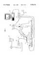
- the substrate 10may be silicon dioxide, glass, lithium niobate or any semi-conducting material used for making electronic components.
- the substratehas an upper planar surface 12, and rests on a support 14 forming part of an xy translation stage 16.
- a container 18 containing curable light guide forming liquid 20, having a nozzle 22,is mounted on an arm 24 of a z-axis actuator 26, which is lowered to dispense liquid and raised during re-positioning of the nozzle.
- the z-axis actuator 26 and xy translation stage 16together form a means for controllably changing the spatial relationship of the nozzle to the substrate.
- the z-axis actuator 26regulates the height of the nozzle above the substrate 10, while the xy translation stage regulates the horizontal location of the nozzle 22 on the substrate 10.
- Flow of liquid 20 from the container 18 and nozzle 22is regulated by means of a dispenser 28.
- the volume of curable light guide forming liquid dispensed per unit lenght of light guide, and hence the width of the light guide,is controlled through a combination of translation speed and pressure in the dispenser. The greater the speed, and/or the lower the pressure, the narrower the light guide.
- the dispenseroperates by applying a regulated air pressure to the surface of the liquid contained in the syringe, forcing the liquid through the dispensing tip 30 of the nozzle 22.
- the xy translation stage 16 and z-axis actuator 26are controlled by controller 32.
- Control signals for the controller 32may be supplied by joystick 34 or by computer 36, for example controlled according to the program filed with the Patent and Trademark Office as a microfiche appendix.
- the curable light guide forming liquid 20is preferably cured using liquid curing radiation, such as from UV source 38 with light guide 42 for delivering the light to the desired location.
- the source 38 of liquid curing radiationmay also be moved over the surface of the substrate in a linear pattern by using the xy translation state.
- a microscope 44may be used to inspect the manufacturing process.
- the nozzle 22is preferably formed from a tube of internal diameter less than about 100 ⁇ m (as for example 50 ⁇ m), but may consist simply of a small aperture in a container.
- a syringe having barrel inside diameter 1 cm with a 50 ⁇ m inside diameter tiphas been found successful.
- a capillary tubemay also be used as the nozzle 22 with liquid supplied from a pump (not shown). In such an instance, only the capillary need be moved, rather than the entire nozzle.
- An alternative embodimentis shown in FIG. 5, in which the nozzle 22 is formed of a first central tube 46 and a second outer tube 48 disposed about the first central tube 46 to form an annulus between them.
- the container 18has separate compartments, one compartment 52 connected to the first central tube 46 and the other compartment 54 connected to the second outer tube 48.
- a curable light guide forming liquidis a liquid having the property that under known conditions, as for example exposure to ultraviolet light, it may undergo reactions that solidify the liquid to yield a material that is at least partially transparent to light and that is capable of guiding light, which typically requires only that the liquid have a boundary and be in a medium with lower index of refraction.
- the index of refraction of the polymer or other curable light guide forming liquidshould be greater than the index of refraction of the substrate or a cladding layer on the substrate.
- a light guidemay be formed on the substrate, for example using the apparatus of the invention, by ejecting the curable light guide forming liquid 20 from the nozzle 22 onto the substrate 10 and curing the curable light guide forming liquid 20 to form an optical element. If the nozzle 22 is not moved during dispensing of the liquid 20 from the nozzle 22, then a lens may be formed. For waveguides, however, the nozzle 22 is moved in a linear pattern (as for example shown in FIG. 2, with the arrow A showing direction of movement) over the surface 12 of the substrate 10 to form a waveguide 56. The liquid 20 must be cured to a solid state, thus forming a waveguide having the linear pattern.
- Curingis preferably achieved by exposing the liquid 20 to ultraviolet radiation immediately after dispensing of the liquid 20 from the nozzle 22.
- the inside of the container 18should be coated with a UV blocking material 58 to prevent curing of the liquid 20 inside the container 18 during dispensing.
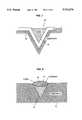
- a light guidemay be formed by exposing only a central portion of the liquid 20 to curing radiation 62 thus forming a narrow strip waveguide region 64.
- the radiation 62may be focused using a lens 66 to reduce the size of the cured region.
- the uncured remainder of the liquid 20may be removed using conventional solvents.
- a cladding 68 for the waveguide 56may be formed by ejecting a second curable light guide forming liquid 70 onto the waveguide core 70.
- the cladding liquid 70should be formed of a material with lower refractive index than the core 72. If the substrate 10 does not have suitable optical properties, a buffer layer 11 may be used to provide the necessary optical properties.
- a waveguide 56may be formed by simultaneously dispensing a core 74 and cladding 76 using a nozzle 22 having central aperture 46 and an annular aperture 48.
- an optical elementmay be formed by directly ejecting a curable light guide forming liquid 20 into a groove 78 formed, as by anisotropic etching, in a semiconductor substrate 10.
- a groove 78may be constructed with sidewalls defined by crystal planes and are therefore extremely smooth.
- the core liquidcan be dispensed directly into the v-groove if the substrate is transparent and has a lower refractive index. If this is not the case, a suitable cladding layer must be formed on the surface of the substrate and on the v-groove walls.
- the optical elementis a waveguide 56, formed of a core by moving the nozzle 22 along the groove 78, while in FIG.
- a cladding 76 of curable cladding forming liquid(lower index of refraction) is first ejected into a groove 78, and then a core 74 (higher index of refraction) deposited on top of the cladding 76, in each case by moving the nozzle 22 along the groove while dispensing liquid.
- a light guidemay be formed with reflective out-of-plane taps 84.
- Taps 84are formed by dispensing drops of reflective material prior to dispensing the waveguide 56. Some of the light propagating in the waveguide 56 will hit the reflective bumps 84 and will radiate upwards. Equal amounts of optical power can be tapped out of the waveguide by grading the size of the bumps; increasing their size as the power in the guide drops.
- a waveguide 57may be formed in layers and have staggered reflective ends 86 for out-of-plane coupling.
- Each waveguide layer 56is formed by dispensing curable light guide forming liquid in a linear pattern and then curing the liquid.
- Each successive waveguide layerfollows the same path to create the stack.
- Small lenses 88may be formed on the under side of the substrate by turning the substrate over and ejecting the curable light guide forming liquid without moving the nozzle 22. Lenses may be stacked in order to control the lens profile and thus the f-number of the lens.
- Multilayered waveguidesmay also involve the use of two or more polymers of different refractive index. In this case a lower index polymer is first deposited, followed by a higher index core material. Finally, a second cladding layer may be deposited over the waveguide core in order to reduce the waveguide propagation losses and protect it from damage.
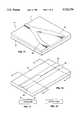
- a branched waveguide pattern or splitter 90may be formed by first dispensing one arm 82 of the branch and then immediately dispensing the other arm 84.
- a silicon dioxide layer 11forms a smooth lower cladding.
- Each branchis formed of an S-bend waveguide.
- a parallel waveguide splittermay be formed by dispensing two closely spaced but separated straight linear waveguides 92 and 94 on a substrate 10 using the same liquid 20 and then curing them.
- the input ends(FIG. 13) are then joined by dispensing the same light guide forming liquid between and connecting the two waveguides 92 and 94 in like manner, to yield connected waveguides at one end (FIG. 13) and divided waveguides at the other end (FIG. 14).
- the dispensing tip 30 of the nozzle 22is first moved to a starting position, the tip 30 is lowered to a height either in contact with, or just above, the substrate surface.
- the vertical position of the substrate surfacemay be memorized by the computer 36 and reset by the user.
- Dispensing of liquidis preferably set to begin when the tip 30 reaches the bottom of its travel and the substrate 10 is then positioned through a linear pattern that may be specified in software or controlled through movement of the joystick 34.
- the dispenseris turned off and the tip 30 is raised.
- the dispense tip 30can then be re-positioned to another location to begin another waveguide branch. For optimal results the dispense tip 30 should be angled as shown in FIG.
- Use of an ultraviolet light sourceincreases the height-to-width ratio of the waveguide 56 (allowing less settling time for the liquid) and prevents contaminants from being introduced while the waveguide 56 is in the liquid state.
- the curing lightis confined to a spot several millimeters in diameter in close proximity to the dispensing tip 30.
- the controller board 32may be used to turn the light on or off.
- the tip 30should be either in contact with the substrate surface or slightly above it.
- the curing sourceshould be placed so that the edge of the UV spot is within a few millimeters of the dispensing tip but is not close enough to cause clogging.
- the light spotshould be large enough so that when forming bends the liquid waveguide still passes under the UV light.
- the core materialmust be optically transparent and have a higher refractive index that the surrounding material. If the substrate 10 is not transparent at the desired optical wavelength or has a high refractive index, a buffer layer 11 must be used between the core and the substrate in order to prevent excessive waveguide losses (See FIGS. 3 and 4).
- the upper cladding materialmay be air or a low index curable liquid.
- the latteris preferred since it protects the waveguide from dirt and/or damage.
- the height-to-width ratio of the waveguidedepends on the viscosity of the liquid, the properties of the surface layer, and the time elapsed before curing.
- the embodiment of FIG. 4is suitable for forming small waveguides suitable for single mode operation, and can be fabricated by selectively dispensing the liquid and then using a focused UV beam to cure only the middle portion. This eliminates the need for the spin coating step which is used in the standard laser writing technique and replaces it with a more selective process.
- Complex structuressuch as 1 ⁇ N or N ⁇ N splitters and combiners may be fabricated by repetitive movement of the dispenser tip 30, which makes the system amenable to automation. If an input and output point are specified, the location of the waveguide branches may be automatically calculated.
- FIG. 15shows waveguide loss measurement for single pass dispensed waveguide on planar substrate. Losses of 0.45 dB/cm at 633 nm were measured by monitoring the scattered power along the length of the waveguide.
- FIG. 16shows waveguide loss measurement for a double pass dispensed waveguide on planar substrate (same polymer used for each pass). Losses of 0.5 dB/cm at 633 nm were measured by monitoring the scattered power along the length of the waveguide. Comparing this result to that in FIG. 15 we can see that there is no significant penalty in the quality of waveguides formed using the multistep technique.
- FIG. 17shows waveguide loss measurement for double pass dispensed waveguide on planar substrate consisting of a high index polymer clad from above by a lower index polymer. Losses of 0.17 dB/cm at 633 nm were measured by monitoring the scattered power along the length of the waveguide.
- FIG. 18shows the intensity distribution at output of the parallel waveguide splitter of FIGS. 12, 13 and 14.
- the waveguidesshould not include any sharp bends and should be continuous and smooth.
- the xy translation stageshould provide at least 1 mm/sec travel speed.
- the waveguide forming processshould occur in a clean environment.
- Splittersshould be dispensed from output to input to reduce effects of surface tension.
- Input sectionshould be cured on last pass only.
- Waveguide endsshould be cleaved if using butt-coupling to fibers.
- input and output fibersshould be secured with cores aligned to substrate surface prior to waveguide fabrication. Waveguides can then be dispensed from fiber to fiber, with the liquid attaching directly to the fiber ends thereby eliminating air gaps. This results in good refractive index matching between fiber and waveguide.
- Y-splittersdue to effects of liquid surface tension during dispensing of second waveguide branch. This can be offset by making the splitter geometry slightly asymmetric. Waveguide cross-section exhibits a low height-to-width ratio when liquid is allowed to settle to steady state before curing. Higher ratios can be obtained by curing immediately after dispensing or by a multistep technique. Y-splitter junctions should be sharp in order to minimize excess losses. This can be achieved by immediate curing. Measures must be taken to prevent formation of liquid beads on the dispensing tip. A slight vacuum may be applied to the dispensing tip when the dispenser is in the OFF state to prevent bead formation.
- the computer described in this applicationmay be a NeXTStation running NeXTStep operating system version 2.1 or higher, available from NeXT Computer Inc., or compatible
- the controllermay be a Newport/Klinger MotionMaster 2000 with A/D, D/A option
- the actuatormay be a Newport/Klinger BMCC series with 76:1 gears
- the translation stagesmay be Newport/Klinger MR series with 63 mm travel
- the dispensermay be an EFD Inc.
- model 900model 900
- the UV sourcemay be an Ultracure 100ss, available from EFOS Inc., all of which products are commonly commercially avaiable.
Landscapes
- Engineering & Computer Science (AREA)
- Physics & Mathematics (AREA)
- Optics & Photonics (AREA)
- Mechanical Engineering (AREA)
- Microelectronics & Electronic Packaging (AREA)
- General Physics & Mathematics (AREA)
- Chemical & Material Sciences (AREA)
- Materials Engineering (AREA)
- Manufacturing & Machinery (AREA)
- Health & Medical Sciences (AREA)
- Ophthalmology & Optometry (AREA)
- Optical Integrated Circuits (AREA)
Abstract
Description
This application is a division of application Ser. No. 08/204,517 filed Mar. 2, 1994, U.S. Pat. No. 5,534,101.
A microfiche appendix consisting of two microfiche and 107 frames forms part of this patent document. The microfiche appendix contains software used to control apparatus used in an implementation of the method of the invention.
This invention relates to methods and apparatus for making integrated optical light guides on substrates.
A portion of the disclosure of this patent document contains material which is subject to copyright protection. The copyright owner has no objection to the facsimile reproduction by anyone of the patent document, as it appears in the Patent and Trademark Office patent file or records, but otherwise reserves all copyright rights whatsoever.
Hybrid integration of photonic and electronic components provides a lower cost alternative to fully monolithic integration. Individual components can be fabricated using preferred materials and techniques and then assembled on a common substrate or carrier. Optical light guides are required for broadband interconnections between the optical and/or optoelectronic devices. To be economically viable these light guides must be low cost and easily manufactured.
As used in this specification, a light guide is a material that is at least partially transparent to light and is capable of guiding light, as for example a lens or a waveguide.
An optical waveguide is comprised of a region of high refractive index material surrounded by materials of lower refractive index. Optical waveguides have been fabricated on a variety of substrates including semiconductors, glass, Lithium Niobate and the like. They are typically formed by first preparing a low-loss planar slab and then defining the waveguide regions using one of a variety of techniques. These techniques include: (1) wet chemical etching, laser-assisted etching, or reactive ion etching (all of which remove material in specific areas to form waveguide ridges); (2) ion bombardment or ion exchange, which create a molecular disorder to alter the refractive index; (3) photopolymerization of organic polymers; (4) photobleaching of organic dyes in polymers; and (5) injection molding.
The processes described above typically require the use of a mask which contains the layout of the waveguides. Modifications to the layout therefore require the fabrication of a new mask which is time consuming and adds expense. Computer-controlled direct write systems are more suitable for rapid prototyping of optical waveguides. Several groups have reported laser writing techniques which selectively cure, through a photochemical process, waveguide regions from a film of liquid polymer see Krchnavek et al., Laser direct writing of channel waveguides using spin-on polymers, J. of Applied Physics, vol. 66, no. 11, 1989!. These systems require that a uniform film be first deposited over the entire substrate. Following the laser writing procedure, the remaining unexposed material is removed. The dimensions of the waveguide are determined by the size of the focused spot used to cure the material. To achieve small features the light source must produce a good quality beam (near Gaussian) which can be tightly focused. This typically requires the use of an expensive UV laser source. In addition, the incident energy level of the light source must be carefully controlled in order to rapidly cure the waveguides without degrading the optical properties.
The inventors have found a simple yet surprisingly effective technique of forming optical elements on a surface of a material. In one aspect of the invention, there is provided a method of forming an optical light guide on the surface of a substrate by ejecting a first curable light guide forming liquid from a nozzle onto the substrate and curing the first curable light guide forming liquid to form an optical element on the surface of the substrate. A waveguide may be formed by moving the nozzle in a linear pattern over the surface of the substrate while ejecting the first curable light guide forming liquid from the nozzle. Curing the first curable light guide forming liquid may include exposing the curable light guide forming liquid to ultraviolet (UV) radiation, and the radiation may be applied to only a small portion of the liquid. A multilayered waveguide may be formed by ejecting a second light guide forming liquid onto the first and curing it. A core and cladding may be formed simultaneously by ejecting core forming liquid from an inner tube and cladding forming liquid from an annulus about the inner tube. The light guide may be formed in a groove or on a planar surface, and a splitter may be formed by branching a second waveguide from a first, or by laying out two parallel waveguides and connecting them.
In a further aspect of the invention, there is provided apparatus for forming a light guide on a substrate. The apparatus preferably includes an xy movable support for the substrate, and a container having a nozzle, the nozzle being movable in relation to the substrate, and a dispenser to regulate dispensing of liquid from the container. Liquid curing radiation may be provided through a source of UV light. According to one aspect of the invention, the nozzle may be formed of a first central tube and a second outer tube disposed about the first central tube to form an annulus between them, the container having separate compartments, one connected to the first central tube and the other connected to the second outer tube.
The apparatus and method allow selective writing of optical light guides. The core of the light guide may be dispensed and cured in a single step with no further processing required (ie. no removal of excess material). The light guide dimensions are determined primarily by the volume of liquid dispensed per unit length of the light guide. An inexpensive light source may therefore be used for curing since there is no requirement for a small focused spot. The same apparatus is also used to form refractive microlenses by depositing small droplets of photocurable polymer.
In the case of planar substrates, the light guides are formed by selective deposition which eliminates the need for preforms, etching, or lift-off. No processing masks are required since the light guide layouts are defined by scalable software routines. This makes the technique particularly attractive for rapid prototyping applications. In comparison with other direct-write schemes, the technique eliminates the requirement for spin coating and excess polymer removal and replaces the ultraviolet laser with an inexpensive light source. Waveguides may also be formed by dispensing a light guide forming liquid into a v-groove in the substrate. These polymer-filled v-groove waveguides require the use of anisotropic etching to form the grooves but offer better control of waveguide cross-section and compatibility with fiber alignment grooves.
There will now be described preferred embodiments of the invention, with reference to the drawings, by way of illustration, in which like numerals denote like elements and in which:
FIG. 1 is a schematic showing an embodiment of an apparatus according to the invention;
FIG. 2 is a side view of a dispensing tip in the process of carrying out an embodiment of the method of the invention;
FIG. 3 is a cross-sectional schematic illustrating a waveguide made according to the method of the invention illustrated in FIG. 2;
FIG. 4 is a cross-section illustrating a manner of carrying out a curing step in the method of the invention;
FIG. 5 is a side view of a dispensing tip in the process of carrying out a further embodiment of the method of the invention;
FIG. 6 is a cross-sectional schematic illustrating a waveguide made according to the method of the invention illustrated in FIG. 5;
FIGS. 7 and 8 illustrate waveguides made in accordance with the invention in which the waveguides are formed in grooves in a substrate;
FIG. 9 is a side view illustrating the manner of propagation of light in a waveguide made according to the invention;
FIG. 10 is a cross-section showing multilayered waveguides made according to the invention;
FIG. 11 is a perspective view of a Y-splitter made according to the invention;
FIG. 12 is a perspective view of a parallel waveguide splitter;
FIG. 13 is a cross-section along theline 13--13 in FIG. 12;
FIG. 14 is a cross-section along theline 14--14 in FIG. 12;
FIGS. 15, 16 and 17 show waveguide losses for several embodiments of the invention; and
FIG. 18 shows an intensity distribution at output of a parallel waveguide splitter made in accordance with the invention.
Referring to FIGS. 1, 2 and 3, there is shown an apparatus according to the invention for forming a light guide on asubstrate 10. Thesubstrate 10 may be silicon dioxide, glass, lithium niobate or any semi-conducting material used for making electronic components. The substrate has an upperplanar surface 12, and rests on asupport 14 forming part of anxy translation stage 16. Acontainer 18 containing curable lightguide forming liquid 20, having anozzle 22, is mounted on anarm 24 of a z-axis actuator 26, which is lowered to dispense liquid and raised during re-positioning of the nozzle. The z-axis actuator 26 andxy translation stage 16 together form a means for controllably changing the spatial relationship of the nozzle to the substrate. The z-axis actuator 26 regulates the height of the nozzle above thesubstrate 10, while the xy translation stage regulates the horizontal location of thenozzle 22 on thesubstrate 10. Flow of liquid 20 from thecontainer 18 andnozzle 22 is regulated by means of adispenser 28. The volume of curable light guide forming liquid dispensed per unit lenght of light guide, and hence the width of the light guide, is controlled through a combination of translation speed and pressure in the dispenser. The greater the speed, and/or the lower the pressure, the narrower the light guide. The dispenser operates by applying a regulated air pressure to the surface of the liquid contained in the syringe, forcing the liquid through the dispensingtip 30 of thenozzle 22. Thexy translation stage 16 and z-axis actuator 26 are controlled bycontroller 32. Control signals for thecontroller 32 may be supplied byjoystick 34 or bycomputer 36, for example controlled according to the program filed with the Patent and Trademark Office as a microfiche appendix. The curable lightguide forming liquid 20 is preferably cured using liquid curing radiation, such as fromUV source 38 withlight guide 42 for delivering the light to the desired location. Thesource 38 of liquid curing radiation may also be moved over the surface of the substrate in a linear pattern by using the xy translation state. Amicroscope 44 may be used to inspect the manufacturing process.
Thenozzle 22 is preferably formed from a tube of internal diameter less than about 100 μm (as for example 50 μm), but may consist simply of a small aperture in a container. A syringe having barrel insidediameter 1 cm with a 50 μm inside diameter tip has been found successful. A capillary tube may also be used as thenozzle 22 with liquid supplied from a pump (not shown). In such an instance, only the capillary need be moved, rather than the entire nozzle. An alternative embodiment is shown in FIG. 5, in which thenozzle 22 is formed of a firstcentral tube 46 and a secondouter tube 48 disposed about the firstcentral tube 46 to form an annulus between them. Thecontainer 18 has separate compartments, onecompartment 52 connected to the firstcentral tube 46 and theother compartment 54 connected to the secondouter tube 48.
The curable lightguide forming liquid 20 is preferably a UV curable polymer (n between 1.5 and 1.6) such asNorland™ 68 optical adhesive (n=1.54) that cures with low shrinkage when exposed to ultraviolet light. In this patent document, a curable light guide forming liquid is a liquid having the property that under known conditions, as for example exposure to ultraviolet light, it may undergo reactions that solidify the liquid to yield a material that is at least partially transparent to light and that is capable of guiding light, which typically requires only that the liquid have a boundary and be in a medium with lower index of refraction.
The index of refraction of the polymer or other curable light guide forming liquid, should be greater than the index of refraction of the substrate or a cladding layer on the substrate. A suitable cladding material is silicon dioxide having an index of refraction of n=1.46. If thesubstrate 10 is unsuitable as a cladding material, abuffer layer 11 may be formed by vapour deposition of silicon dioxide on thesubstrate 10. Thebuffer layer 11 or the substrate itself thus acts as the lower cladding layer for a waveguide deposited on the substrate. Alternatively, a two-stage dispensing technique may be used in which a low index cladding forming material is first dispensed and cured and a second higher index light guide forming liquid is then deposited on top.
A light guide may be formed on the substrate, for example using the apparatus of the invention, by ejecting the curable light guide forming liquid 20 from thenozzle 22 onto thesubstrate 10 and curing the curable lightguide forming liquid 20 to form an optical element. If thenozzle 22 is not moved during dispensing of the liquid 20 from thenozzle 22, then a lens may be formed. For waveguides, however, thenozzle 22 is moved in a linear pattern (as for example shown in FIG. 2, with the arrow A showing direction of movement) over thesurface 12 of thesubstrate 10 to form awaveguide 56. The liquid 20 must be cured to a solid state, thus forming a waveguide having the linear pattern. Curing is preferably achieved by exposing the liquid 20 to ultraviolet radiation immediately after dispensing of the liquid 20 from thenozzle 22. The inside of thecontainer 18 should be coated with aUV blocking material 58 to prevent curing of the liquid 20 inside thecontainer 18 during dispensing.
As shown in FIG. 4, a light guide may be formed by exposing only a central portion of the liquid 20 to curingradiation 62 thus forming a narrowstrip waveguide region 64. Theradiation 62 may be focused using alens 66 to reduce the size of the cured region. The uncured remainder of the liquid 20 may be removed using conventional solvents.
As shown in FIG. 3, acladding 68 for thewaveguide 56 may be formed by ejecting a second curable lightguide forming liquid 70 onto thewaveguide core 70. Thecladding liquid 70 should be formed of a material with lower refractive index than thecore 72. If thesubstrate 10 does not have suitable optical properties, abuffer layer 11 may be used to provide the necessary optical properties. As illustrated in FIGS. 5 and 6, awaveguide 56 may be formed by simultaneously dispensing acore 74 andcladding 76 using anozzle 22 havingcentral aperture 46 and anannular aperture 48.
As shown in FIGS. 7 and 8, an optical element may be formed by directly ejecting a curable lightguide forming liquid 20 into agroove 78 formed, as by anisotropic etching, in asemiconductor substrate 10. Such agroove 78 may be constructed with sidewalls defined by crystal planes and are therefore extremely smooth. The core liquid can be dispensed directly into the v-groove if the substrate is transparent and has a lower refractive index. If this is not the case, a suitable cladding layer must be formed on the surface of the substrate and on the v-groove walls. In FIG. 7, the optical element is awaveguide 56, formed of a core by moving thenozzle 22 along thegroove 78, while in FIG. 8, acladding 76 of curable cladding forming liquid (lower index of refraction) is first ejected into agroove 78, and then a core 74 (higher index of refraction) deposited on top of thecladding 76, in each case by moving thenozzle 22 along the groove while dispensing liquid.
As shown in FIG. 9, a light guide may be formed with reflective out-of-plane taps 84.Taps 84 are formed by dispensing drops of reflective material prior to dispensing thewaveguide 56. Some of the light propagating in thewaveguide 56 will hit thereflective bumps 84 and will radiate upwards. Equal amounts of optical power can be tapped out of the waveguide by grading the size of the bumps; increasing their size as the power in the guide drops.
As shown in FIG. 10, awaveguide 57 may be formed in layers and have staggered reflective ends 86 for out-of-plane coupling. Eachwaveguide layer 56 is formed by dispensing curable light guide forming liquid in a linear pattern and then curing the liquid. Each successive waveguide layer follows the same path to create the stack.Small lenses 88 may be formed on the under side of the substrate by turning the substrate over and ejecting the curable light guide forming liquid without moving thenozzle 22. Lenses may be stacked in order to control the lens profile and thus the f-number of the lens.
If a single polymer is used to form a stacked multilayered waveguide, the result is a composite waveguide cross-section with increased height-to-width ratio that couples light more efficiently to optical fiber. Multilayered waveguides may also involve the use of two or more polymers of different refractive index. In this case a lower index polymer is first deposited, followed by a higher index core material. Finally, a second cladding layer may be deposited over the waveguide core in order to reduce the waveguide propagation losses and protect it from damage.
As shown in FIG. 11, a branched waveguide pattern orsplitter 90 may be formed by first dispensing onearm 82 of the branch and then immediately dispensing theother arm 84. Asilicon dioxide layer 11 forms a smooth lower cladding. Each branch is formed of an S-bend waveguide.
As shown in FIGS. 12, 13 and 14, a parallel waveguide splitter may be formed by dispensing two closely spaced but separated straightlinear waveguides substrate 10 using thesame liquid 20 and then curing them. The input ends (FIG. 13) are then joined by dispensing the same light guide forming liquid between and connecting the twowaveguides
To fabricate a waveguide branch the dispensingtip 30 of thenozzle 22 is first moved to a starting position, thetip 30 is lowered to a height either in contact with, or just above, the substrate surface. The vertical position of the substrate surface may be memorized by thecomputer 36 and reset by the user. Dispensing of liquid is preferably set to begin when thetip 30 reaches the bottom of its travel and thesubstrate 10 is then positioned through a linear pattern that may be specified in software or controlled through movement of thejoystick 34. When the end point of the linear pattern ofwaveguide 56 is reached the dispenser is turned off and thetip 30 is raised. The dispensetip 30 can then be re-positioned to another location to begin another waveguide branch. For optimal results the dispensetip 30 should be angled as shown in FIG. 2, preferably at 45°. Use of an ultraviolet light source increases the height-to-width ratio of the waveguide 56 (allowing less settling time for the liquid) and prevents contaminants from being introduced while thewaveguide 56 is in the liquid state. The curing light is confined to a spot several millimeters in diameter in close proximity to the dispensingtip 30. Thecontroller board 32 may be used to turn the light on or off.
During dispensing thetip 30 should be either in contact with the substrate surface or slightly above it. The curing source should be placed so that the edge of the UV spot is within a few millimeters of the dispensing tip but is not close enough to cause clogging. The light spot should be large enough so that when forming bends the liquid waveguide still passes under the UV light. The core material must be optically transparent and have a higher refractive index that the surrounding material. If thesubstrate 10 is not transparent at the desired optical wavelength or has a high refractive index, abuffer layer 11 must be used between the core and the substrate in order to prevent excessive waveguide losses (See FIGS. 3 and 4). The upper cladding material may be air or a low index curable liquid. The latter is preferred since it protects the waveguide from dirt and/or damage. The height-to-width ratio of the waveguide depends on the viscosity of the liquid, the properties of the surface layer, and the time elapsed before curing. The embodiment of FIG. 4 is suitable for forming small waveguides suitable for single mode operation, and can be fabricated by selectively dispensing the liquid and then using a focused UV beam to cure only the middle portion. This eliminates the need for the spin coating step which is used in the standard laser writing technique and replaces it with a more selective process.
Complex structures such as 1×N or N×N splitters and combiners may be fabricated by repetitive movement of thedispenser tip 30, which makes the system amenable to automation. If an input and output point are specified, the location of the waveguide branches may be automatically calculated.
Waveguide widths of less than 100 μm have been obtained by using the process of the invention, with excellent uniformity over several centimeters in length. FIG. 15 shows waveguide loss measurement for single pass dispensed waveguide on planar substrate. Losses of 0.45 dB/cm at 633 nm were measured by monitoring the scattered power along the length of the waveguide. FIG. 16 shows waveguide loss measurement for a double pass dispensed waveguide on planar substrate (same polymer used for each pass). Losses of 0.5 dB/cm at 633 nm were measured by monitoring the scattered power along the length of the waveguide. Comparing this result to that in FIG. 15 we can see that there is no significant penalty in the quality of waveguides formed using the multistep technique. These waveguides offer the benefit of improved coupling to optical fibers and better alignment tolerance. FIG. 17 shows waveguide loss measurement for double pass dispensed waveguide on planar substrate consisting of a high index polymer clad from above by a lower index polymer. Losses of 0.17 dB/cm at 633 nm were measured by monitoring the scattered power along the length of the waveguide. FIG. 18 shows the intensity distribution at output of the parallel waveguide splitter of FIGS. 12, 13 and 14.
The waveguides should not include any sharp bends and should be continuous and smooth. The xy translation stage should provide at least 1 mm/sec travel speed. The waveguide forming process should occur in a clean environment. Splitters should be dispensed from output to input to reduce effects of surface tension. Input section should be cured on last pass only. Waveguide ends should be cleaved if using butt-coupling to fibers. For best results, input and output fibers should be secured with cores aligned to substrate surface prior to waveguide fabrication. Waveguides can then be dispensed from fiber to fiber, with the liquid attaching directly to the fiber ends thereby eliminating air gaps. This results in good refractive index matching between fiber and waveguide. Slight asymmetry is usually observed in Y-splitters due to effects of liquid surface tension during dispensing of second waveguide branch. This can be offset by making the splitter geometry slightly asymmetric. Waveguide cross-section exhibits a low height-to-width ratio when liquid is allowed to settle to steady state before curing. Higher ratios can be obtained by curing immediately after dispensing or by a multistep technique. Y-splitter junctions should be sharp in order to minimize excess losses. This can be achieved by immediate curing. Measures must be taken to prevent formation of liquid beads on the dispensing tip. A slight vacuum may be applied to the dispensing tip when the dispenser is in the OFF state to prevent bead formation.
The computer described in this application may be a NeXTStation running NeXTStep operating system version 2.1 or higher, available from NeXT Computer Inc., or compatible, the controller may be a Newport/Klinger MotionMaster 2000 with A/D, D/A option, the actuator may be a Newport/Klinger BMCC series with 76:1 gears, the translation stages may be Newport/Klinger MR series with 63 mm travel, the dispenser may be an EFD Inc., model 900 and the UV source may be an Ultracure 100ss, available from EFOS Inc., all of which products are commonly commercially avaiable.
A person skilled in the art could make immaterial modifications to the invention described and claimed in this patent without departing from the essence of the invention.
Claims (15)
1. Apparatus for forming a light guide on a substrate, the substrate having a surface, the apparatus comprising:
a support for the substrate;
a container having a nozzle;
an xy translation stage, the substrate being supported on the xy translation stage for translational movement in a plane defined by x and y axes;
a z-axis actuator, the container being mounted on the z-axis actuator for movement by the z-axis actuator in a direction perpendicular to the plane defined by the x and y axes from a position close to the substrate to a position away from the substrate;
a source of liquid curing radiation mounted to provide liquid curing radiation in the direction of the substrate; and
means to regulate dispensing of liquid from the container.
2. The apparatus of claim 1 in which the nozzle is formed of a first central tube and a second outer tube disposed about the first central tube to form an annulus between them, the container having separate compartments, one connected to the first central tube and the other connected to the second outer tube.
3. The apparatus of claim 1 further comprising means to move the source of liquid curing radiation over the surface of the substrate in a linear pattern.
4. A method of forming an optical element on a substrate used for making electronic components, the substrate having a surface layer, comprising the steps of:
ejecting a first curable light guide forming liquid from a nozzle onto the substrate, while the nozzle is in contact with or slightly above the substrate; and
curing the first curable light guide forming liquid to form an optical element on the surface of the substrate, the optical element forming a light guide for light passing through or along the substrate.
5. The method of claim 4 in which the first curable light guide forming liquid is continuously ejected from the nozzle onto the surface layer in a defined pattern, the optical element forming a light guide having the defined pattern for light passing through or along the substrate.
6. The method of claim 5 in which the defined pattern is a linear pattern, thereby forming a first optical element having the linear pattern.
7. The method of claim 6 in which the nozzle includes a central aperture and an annular aperture formed about the central aperture, the method further including ejecting a second curable light guide forming liquid from the annular aperture while ejecting the first curable light guide forming liquid.
8. The method of claim 5 in which curing the first curable light guide forming liquid includes exposing the first curable light guide forming liquid to ultraviolet radiation.
9. The method of claim 8 in which only a central portion of the liquid is exposed to curing radiation.
10. The method of claim 5 further comprising:
ejecting a second curable light guide forming liquid onto the optical element and curing the second curable light guide forming liquid to form a stacked optical element.
11. The method of claim 5 further including ejecting a second curable light guide forming liquid, having a lower index of refraction than that of the first curable light guide forming liquid, onto the waveguide and curing the second curable light guide forming liquid, to form a cladding for the waveguide.
12. The method of claim 5 in which the first curable light guide forming liquid is ejected into a groove in the substrate.
13. The method of claim 5 further including forming a branched waveguide pattern.
14. The method of claim 13 in which the branched waveguide pattern is formed by forming a first linear waveguide by the method of claim 7 using a first curable light guide forming liquid and forming a second linear waveguide parallel to the first linear waveguide by the method of claim 7 using the first curable light guide forming liquid and ejecting further of the first curable light guide forming liquid between and connecting the first and second linear waveguide.
15. The method of claim 4 in which the nozzle is not moved while ejecting the first curable light guide forming liquid, whereby a lens is formed.
Priority Applications (1)
| Application Number | Priority Date | Filing Date | Title |
|---|---|---|---|
| US08/676,832US5723176A (en) | 1994-03-02 | 1996-07-08 | Method and apparatus for making optical components by direct dispensing of curable liquid |
Applications Claiming Priority (2)
| Application Number | Priority Date | Filing Date | Title |
|---|---|---|---|
| US08/204,517US5534101A (en) | 1994-03-02 | 1994-03-02 | Method and apparatus for making optical components by direct dispensing of curable liquid |
| US08/676,832US5723176A (en) | 1994-03-02 | 1996-07-08 | Method and apparatus for making optical components by direct dispensing of curable liquid |
Related Parent Applications (1)
| Application Number | Title | Priority Date | Filing Date |
|---|---|---|---|
| US08/204,517DivisionUS5534101A (en) | 1994-03-02 | 1994-03-02 | Method and apparatus for making optical components by direct dispensing of curable liquid |
Publications (1)
| Publication Number | Publication Date |
|---|---|
| US5723176Atrue US5723176A (en) | 1998-03-03 |
Family
ID=22758231
Family Applications (2)
| Application Number | Title | Priority Date | Filing Date |
|---|---|---|---|
| US08/204,517Expired - Fee RelatedUS5534101A (en) | 1994-03-02 | 1994-03-02 | Method and apparatus for making optical components by direct dispensing of curable liquid |
| US08/676,832Expired - Fee RelatedUS5723176A (en) | 1994-03-02 | 1996-07-08 | Method and apparatus for making optical components by direct dispensing of curable liquid |
Family Applications Before (1)
| Application Number | Title | Priority Date | Filing Date |
|---|---|---|---|
| US08/204,517Expired - Fee RelatedUS5534101A (en) | 1994-03-02 | 1994-03-02 | Method and apparatus for making optical components by direct dispensing of curable liquid |
Country Status (1)
| Country | Link |
|---|---|
| US (2) | US5534101A (en) |
Cited By (91)
| Publication number | Priority date | Publication date | Assignee | Title |
|---|---|---|---|---|
| US6106622A (en)* | 1997-12-16 | 2000-08-22 | Eastman Kodak Company | Forming optical structures on receivers |
| EP1151839A1 (en)* | 2000-05-01 | 2001-11-07 | Sony Chemicals Corporation | Process for producing ridgy resin film and recording medium |
| US6343171B1 (en) | 1998-10-09 | 2002-01-29 | Fujitsu Limited | Systems based on opto-electronic substrates with electrical and optical interconnections and methods for making |
| US20020027300A1 (en)* | 2000-02-24 | 2002-03-07 | Hartmann Daniel M. | Precision fabrication of diverse polymer microstructures by use of the hydrophobic effect, including microlens arrays, microlenses self-aligned to optical fibers, conductive bump bonds self-aligned to bump pads, and bonds between mutually perpendicular substrates |
| US20020039624A1 (en)* | 2000-10-04 | 2002-04-04 | Dainippon Screen Mfg. Co., Ltd. | Method and apparatus for forming barrier ribs for use in flat panel displays |
| US20020094496A1 (en)* | 2000-07-17 | 2002-07-18 | Choi Byung J. | Method and system of automatic fluid dispensing for imprint lithography processes |
| US20020093122A1 (en)* | 2000-08-01 | 2002-07-18 | Choi Byung J. | Methods for high-precision gap and orientation sensing between a transparent template and substrate for imprint lithography |
| US20020150398A1 (en)* | 2000-08-21 | 2002-10-17 | Choi Byung J. | Flexure based macro motion translation stage |
| US20020196510A1 (en)* | 2001-04-04 | 2002-12-26 | Hietala Vincent Mark | Method and system for decoding multilevel signals |
| US20030030873A1 (en)* | 2001-05-09 | 2003-02-13 | Quellan, Inc. | High-speed adjustable multilevel light modulation |
| US20030048070A1 (en)* | 2001-09-13 | 2003-03-13 | Dainippon Screen Mfg. Co., Ltd. | Method and apparatus for forming barrier ribs for use in flat panel displays, and back plates for flat panel displays manufactured by this method |
| US20030072050A1 (en)* | 2001-03-29 | 2003-04-17 | Quellan, Inc. | Multilevel pulse position modulation for efficient fiber optic communication |
| US20030156655A1 (en)* | 2002-02-15 | 2003-08-21 | Quellan, Inc. | Multi-level signal clock recovery technique |
| US6611635B1 (en) | 1998-10-09 | 2003-08-26 | Fujitsu Limited | Opto-electronic substrates with electrical and optical interconnections and methods for making |
| US20030169195A1 (en)* | 2002-03-08 | 2003-09-11 | Quellan, Inc. | High-speed analog-to-digital converter using a unique gray code |
| US20030198478A1 (en)* | 2002-04-23 | 2003-10-23 | Quellan, Inc. | Method and system for generating and decoding a bandwidth efficient multi-level signal |
| US20030215577A1 (en)* | 2002-05-16 | 2003-11-20 | Willson Carlton Grant | Method and system for fabricating nanoscale patterns in light curable compositions using an electric field |
| US20030226886A1 (en)* | 2002-06-10 | 2003-12-11 | Takashi Kakinuma | Business card information management system |
| US6669801B2 (en) | 2000-01-21 | 2003-12-30 | Fujitsu Limited | Device transfer method |
| US20040007799A1 (en)* | 2002-07-11 | 2004-01-15 | Choi Byung Jin | Formation of discontinuous films during an imprint lithography process |
| US20040012433A1 (en)* | 2002-07-15 | 2004-01-22 | Quellan, Inc. | Adaptive noise filtering and equalization for optimal high speed multilevel signal decoding |
| US6684007B2 (en) | 1998-10-09 | 2004-01-27 | Fujitsu Limited | Optical coupling structures and the fabrication processes |
| US20040022888A1 (en)* | 2002-08-01 | 2004-02-05 | Sreenivasan Sidlgata V. | Alignment systems for imprint lithography |
| US6690845B1 (en) | 1998-10-09 | 2004-02-10 | Fujitsu Limited | Three-dimensional opto-electronic modules with electrical and optical interconnections and methods for making |
| US6696220B2 (en) | 2000-10-12 | 2004-02-24 | Board Of Regents, The University Of Texas System | Template for room temperature, low pressure micro-and nano-imprint lithography |
| US20040038552A1 (en)* | 2002-08-23 | 2004-02-26 | Watts Michael P.C. | Method for fabricating bulbous-shaped vias |
| US6706546B2 (en) | 1998-10-09 | 2004-03-16 | Fujitsu Limited | Optical reflective structures and method for making |
| US20040065976A1 (en)* | 2002-10-04 | 2004-04-08 | Sreenivasan Sidlgata V. | Method and a mold to arrange features on a substrate to replicate features having minimal dimensional variability |
| US20040089979A1 (en)* | 2002-11-13 | 2004-05-13 | Molecular Imprints, Inc. | Method of reducing pattern distortions during imprint lithography processes |
| US6736898B2 (en)* | 1998-11-05 | 2004-05-18 | Basf Aktiengesellschaft | Method and means of producing cured coating films |
| US20040112153A1 (en)* | 2002-12-12 | 2004-06-17 | Molecular Imprints, Inc. | Method and system for determining characteristics of substrates employing fluid geometries |
| US20040124566A1 (en)* | 2002-07-11 | 2004-07-01 | Sreenivasan Sidlgata V. | Step and repeat imprint lithography processes |
| US6785447B2 (en) | 1998-10-09 | 2004-08-31 | Fujitsu Limited | Single and multilayer waveguides and fabrication process |
| US20040168613A1 (en)* | 2003-02-27 | 2004-09-02 | Molecular Imprints, Inc. | Composition and method to form a release layer |
| US20040170770A1 (en)* | 2003-02-27 | 2004-09-02 | Molecular Imprints, Inc. | Method to reduce adhesion between a polymerizable layer and a substrate employing a fluorine-containing layer |
| US6805902B1 (en)* | 2000-02-28 | 2004-10-19 | Microfab Technologies, Inc. | Precision micro-optical elements and the method of making precision micro-optical elements |
| US20040241324A1 (en)* | 2002-07-09 | 2004-12-02 | Molecular Imprints, Inc. | System for dispensing liquids |
| US20040256764A1 (en)* | 2003-06-17 | 2004-12-23 | University Of Texas System Board Of Regents | Method to reduce adhesion between a conformable region and a pattern of a mold |
| US20040257561A1 (en)* | 2000-11-24 | 2004-12-23 | Takao Nakagawa | Apparatus and method for sampling |
| US6845184B1 (en) | 1998-10-09 | 2005-01-18 | Fujitsu Limited | Multi-layer opto-electronic substrates with electrical and optical interconnections and methods for making |
| US20050030884A1 (en)* | 2003-08-07 | 2005-02-10 | Quellan, Inc. | Method and system for crosstalk cancellation |
| US20050061773A1 (en)* | 2003-08-21 | 2005-03-24 | Byung-Jin Choi | Capillary imprinting technique |
| US20050064641A1 (en)* | 1994-09-26 | 2005-03-24 | Semiconductor Energy Laboratory Co., Ltd. | Solution applying apparatus and method |
| US6873087B1 (en) | 1999-10-29 | 2005-03-29 | Board Of Regents, The University Of Texas System | High precision orientation alignment and gap control stages for imprint lithography processes |
| US20050067379A1 (en)* | 2003-09-25 | 2005-03-31 | Molecular Imprints, Inc. | Imprint lithography template having opaque alignment marks |
| US20050072755A1 (en)* | 2003-10-02 | 2005-04-07 | University Of Texas System Board Of Regents | Single phase fluid imprint lithography method |
| US20050076831A1 (en)* | 2001-05-30 | 2005-04-14 | Allen Gilliard | Method and apparatus for applying a coating to an ophthalmic lens |
| EP1531347A1 (en)* | 2003-11-13 | 2005-05-18 | Forschungszentrum Karlsruhe GmbH | Process and equipment for manufacturing of liquid optical waveguides |
| US20050106321A1 (en)* | 2003-11-14 | 2005-05-19 | Molecular Imprints, Inc. | Dispense geometery to achieve high-speed filling and throughput |
| US6908861B2 (en) | 2002-07-11 | 2005-06-21 | Molecular Imprints, Inc. | Method for imprint lithography using an electric field |
| US6916584B2 (en) | 2002-08-01 | 2005-07-12 | Molecular Imprints, Inc. | Alignment methods for imprint lithography |
| US20050160011A1 (en)* | 2004-01-20 | 2005-07-21 | Molecular Imprints, Inc. | Method for concurrently employing differing materials to form a layer on a substrate |
| US20050156353A1 (en)* | 2004-01-15 | 2005-07-21 | Watts Michael P. | Method to improve the flow rate of imprinting material |
| US6921615B2 (en) | 2000-07-16 | 2005-07-26 | Board Of Regents, The University Of Texas System | High-resolution overlay alignment methods for imprint lithography |
| US20050160934A1 (en)* | 2004-01-23 | 2005-07-28 | Molecular Imprints, Inc. | Materials and methods for imprint lithography |
| US20050180520A1 (en)* | 2003-12-22 | 2005-08-18 | Quellan, Inc. | Method and system for slicing a communication signal |
| US20050187339A1 (en)* | 2004-02-23 | 2005-08-25 | Molecular Imprints, Inc. | Materials for imprint lithography |
| US20050192421A1 (en)* | 2004-02-27 | 2005-09-01 | Molecular Imprints, Inc. | Composition for an etching mask comprising a silicon-containing material |
| US20050189676A1 (en)* | 2004-02-27 | 2005-09-01 | Molecular Imprints, Inc. | Full-wafer or large area imprinting with multiple separated sub-fields for high throughput lithography |
| US20050226353A1 (en)* | 2003-11-17 | 2005-10-13 | Quellan, Inc. | Method and system for antenna interference cancellation |
| US20050274219A1 (en)* | 2004-06-01 | 2005-12-15 | Molecular Imprints, Inc. | Method and system to control movement of a body for nano-scale manufacturing |
| US20050276919A1 (en)* | 2004-06-01 | 2005-12-15 | Molecular Imprints, Inc. | Method for dispensing a fluid on a substrate |
| US20050275311A1 (en)* | 2004-06-01 | 2005-12-15 | Molecular Imprints, Inc. | Compliant device for nano-scale manufacturing |
| US20060121728A1 (en)* | 2004-12-07 | 2006-06-08 | Molecular Imprints, Inc. | Method for fast filling of templates for imprint lithography using on template dispense |
| US20060145398A1 (en)* | 2004-12-30 | 2006-07-06 | Board Of Regents, The University Of Texas System | Release layer comprising diamond-like carbon (DLC) or doped DLC with tunable composition for imprint lithography templates and contact masks |
| US20060178157A1 (en)* | 2004-12-14 | 2006-08-10 | Quellan, Inc. | Method and system for reducing signal interference |
| US20060201419A1 (en)* | 1999-10-12 | 2006-09-14 | Toto Ltd. | Apparatus for forming composite structures |
| US7173551B2 (en) | 2000-12-21 | 2007-02-06 | Quellan, Inc. | Increasing data throughput in optical fiber transmission systems |
| US20070060059A1 (en)* | 2004-12-14 | 2007-03-15 | Quellan, Inc. | Method and system for automatic control in an interference cancellation device |
| US20070064923A1 (en)* | 2003-08-07 | 2007-03-22 | Quellan, Inc. | Method and system for signal emulation |
| US20070222654A1 (en)* | 2001-03-29 | 2007-09-27 | Quellan, Inc. | Increasing data throughput in optical fiber transmission systems |
| US20070231981A1 (en)* | 2006-04-03 | 2007-10-04 | Molecular Imprints, Inc. | Patterning a Plurality of Fields on a Substrate to Compensate for Differing Evaporation Times |
| US20070228593A1 (en)* | 2006-04-03 | 2007-10-04 | Molecular Imprints, Inc. | Residual Layer Thickness Measurement and Correction |
| US20070253495A1 (en)* | 2006-04-26 | 2007-11-01 | Quellan, Inc. | Method and system for reducing radiated emissions from a communications channel |
| US20080014367A1 (en)* | 2006-05-01 | 2008-01-17 | Rpo Pty Limited | Low Volatility Polymers for Two-Stage Deposition Processes |
| US20080097065A1 (en)* | 2004-02-27 | 2008-04-24 | Molecular Imprints, Inc. | Composition for an etching mask comprising a silicon-containing material |
| CN100395098C (en)* | 2005-09-16 | 2008-06-18 | 上海电力学院 | Three-dimensional printing molding equipment and method |
| US20080141862A1 (en)* | 2003-10-02 | 2008-06-19 | Molecular Imprints, Inc. | Single Phase Fluid Imprint Lithography Method |
| US20080274333A1 (en)* | 2007-04-27 | 2008-11-06 | Toto Ltd. | Composite structure and production method thereof |
| US20090037004A1 (en)* | 2000-10-12 | 2009-02-05 | Molecular Imprints, Inc. | Method and System to Control Movement of a Body for Nano-Scale Manufacturing |
| FR2934902A1 (en)* | 2008-08-05 | 2010-02-12 | Franck Andre Marie Guigan | Printed optical element e.g. microlens, fabricating method for e.g. optical circuit, involves depositing liquid substance on substrate by opposition of fabrication techniques comprising deposition of solid substance |
| US20100047452A1 (en)* | 2008-08-21 | 2010-02-25 | National Taiwan University | Capillary coating devices and methods |
| US7934144B2 (en) | 2002-11-12 | 2011-04-26 | Quellan, Inc. | High-speed analog-to-digital conversion with improved robustness to timing uncertainty |
| US20110116152A1 (en)* | 2008-05-13 | 2011-05-19 | Franck Guigan | Printed Optical Members |
| US20110151202A1 (en)* | 2009-12-18 | 2011-06-23 | Feinstein Casey J | Controllable Placement of Liquid Adhesive on Substrate |
| CN102141650A (en)* | 2009-12-03 | 2011-08-03 | 三星电子株式会社 | Optical device and manufacturing method thereof |
| US20110206381A1 (en)* | 2010-02-25 | 2011-08-25 | Samsung Electronics Co., Ltd. | Optical serializing/deserializing apparatus and method and method of manufacturing same |
| US8840235B2 (en) | 2010-06-07 | 2014-09-23 | Luxexcel Holding Bv. | Print head, upgrade kit for a conventional inkjet printer, inkjet printer and method for printing optical structures |
| US9192960B2 (en) | 2011-12-13 | 2015-11-24 | 3M Innovative Properties Company | Contact coating by use of a manifold provided with capillary tubes |
| US20170031038A1 (en)* | 2015-07-31 | 2017-02-02 | General Electric Company | Light guide array for pet detector fabrication methods and apparatus |
| US10365413B2 (en) | 2009-02-14 | 2019-07-30 | Luxexcel Holding B.V. | Device for directing light beams, illustration device, method for producing a device and an illustration device |
Families Citing this family (42)
| Publication number | Priority date | Publication date | Assignee | Title |
|---|---|---|---|---|
| US6769618B1 (en) | 1992-02-12 | 2004-08-03 | Lenscard U.S., Llc | Wallet card with a magnifying lens and light |
| US5856661A (en)* | 1993-02-12 | 1999-01-05 | Universal Magnifier Llc | Credit card with magnifying lens formed with a radiation-curable resin |
| US6176430B1 (en) | 1992-02-12 | 2001-01-23 | Lenscard U.S. Llc | Method for making a wallet card with an integral magnifying lens |
| US6817532B2 (en)* | 1992-02-12 | 2004-11-16 | Lenscard U.S., Llc | Wallet card with built-in light |
| EP0807017B1 (en)* | 1995-02-02 | 1999-10-20 | Novartis AG | Process for the manufacture of moulded articles that are partly coloured or have regions of different colours |
| JP3819095B2 (en)* | 1996-01-05 | 2006-09-06 | 富士ゼロックス株式会社 | Optical transmission line forming method, optical transmission line forming apparatus, and optical circuit |
| US6355198B1 (en)* | 1996-03-15 | 2002-03-12 | President And Fellows Of Harvard College | Method of forming articles including waveguides via capillary micromolding and microtransfer molding |
| DE19631736A1 (en)* | 1996-08-06 | 1998-02-12 | Stm Sensor Technologie Muenche | Method and device for manufacturing lenses of micro-optical systems and light transmitter / light receiver system |
| DE19633407A1 (en)* | 1996-08-19 | 1998-02-26 | Fraunhofer Ges Forschung | Device and method for applying photoresist to non-flat base body surfaces for photolithographic processes |
| JP2877125B2 (en)* | 1997-02-14 | 1999-03-31 | 日本電気株式会社 | Waveguide type optical arrester |
| US5932151A (en)* | 1997-09-29 | 1999-08-03 | Imation Corp. | Method of making a flexible lens |
| US6002524A (en)* | 1997-09-29 | 1999-12-14 | Imation Corp. | Flexible lens |
| US6108025A (en)* | 1997-09-29 | 2000-08-22 | Eastman Kodak Company | Optical scanner system having a laser beam power attentuation mechanism |
| US6057537A (en)* | 1997-09-29 | 2000-05-02 | Eastman Kodak Company | Optical scanner feedback system having a reflected cylinder lens |
| JP3482849B2 (en) | 1997-12-16 | 2004-01-06 | 富士ゼロックス株式会社 | Optical transmission path forming device |
| US5952018A (en)* | 1998-03-18 | 1999-09-14 | Eastman Kodak Company | Injection mold cavity and method for making the same |
| US6039553A (en)* | 1998-12-02 | 2000-03-21 | 3M Innovative Properties Company | Apparatus for molding light extraction structures onto a light guide |
| US6094287A (en)* | 1998-12-03 | 2000-07-25 | Eastman Kodak Company | Wobble correcting monogon scanner for a laser imaging system |
| US6692573B1 (en)* | 2000-06-01 | 2004-02-17 | Agilent Technologies, Inc. | Automated pitch button dispensing station and method |
| JP2003107263A (en)* | 2001-09-26 | 2003-04-09 | Sumitomo Bakelite Co Ltd | Method for manufacturing optical waveguide |
| US20030230323A1 (en)* | 2002-06-14 | 2003-12-18 | Taiwan Semiconductor Manufacturing Co., Ltd. | Apparatus and method for improving scrubber cleaning |
| US7024065B2 (en)* | 2002-07-09 | 2006-04-04 | Lucent Technologies Inc. | Optical waveguide device and method of manufacture therefor |
| JP3987404B2 (en)* | 2002-09-27 | 2007-10-10 | セイコーエプソン株式会社 | Optical waveguide and manufacturing method thereof, circuit board, optical module, and optical transmission device |
| KR20040048312A (en)* | 2002-12-02 | 2004-06-07 | 롬 앤드 하스 일렉트로닉 머트어리얼즈, 엘.엘.씨 | Methods of forming waveguides and waveguides formed therefrom |
| US20040151828A1 (en)* | 2003-02-04 | 2004-08-05 | Anis Zribi | Method for fabrication and alignment of micro and nanoscale optics using surface tension gradients |
| US7024082B2 (en)* | 2003-05-16 | 2006-04-04 | Eastman Kodak Company | Apparatus and method for forming an optical converter |
| JP3998204B2 (en)* | 2003-09-17 | 2007-10-24 | 壽一 久保 | Optical fiber wiring method and apparatus |
| TW200720772A (en)* | 2005-11-18 | 2007-06-01 | Hon Hai Prec Ind Co Ltd | Method of producing light guide plate, method for making mold of light guide plate and exploitation process of light guide plate |
| WO2007128039A1 (en)* | 2006-05-01 | 2007-11-15 | Rpo Pty Limited | Waveguide materials for optical touch screens |
| US7811640B2 (en)* | 2006-05-02 | 2010-10-12 | Rpo Pty Limited | Methods for fabricating polymer optical waveguides on large area panels |
| FR2901614A1 (en)* | 2006-05-23 | 2007-11-30 | St Microelectronics Rousset | METHOD FOR MANUFACTURING LENSES, IN PARTICULAR FOR CMOS IMAGER |
| US10090076B2 (en)* | 2009-06-22 | 2018-10-02 | Condalign As | Anisotropic conductive polymer material |
| JP6125431B2 (en)* | 2010-12-15 | 2017-05-10 | コンダリン エーエス | Method for forming a UV curable conductive composition and composition formed thereby |
| JP6038787B2 (en)* | 2011-06-27 | 2016-12-07 | 学校法人慶應義塾 | Manufacturing method of optical waveguide |
| DE102014215061A1 (en)* | 2014-07-31 | 2016-02-04 | Fraunhofer-Gesellschaft zur Förderung der angewandten Forschung e.V. | Micromechanical component and process for its preparation |
| CN104345359B (en)* | 2014-10-28 | 2017-01-18 | 京东方科技集团股份有限公司 | Micro lens array, manufacturing method of micro lens array, image obtaining device and display device |
| JP6147442B2 (en)* | 2014-11-07 | 2017-06-14 | 古河電気工業株式会社 | Method for manufacturing coated optical fiber |
| US20180065317A1 (en)* | 2016-09-06 | 2018-03-08 | Cc3D Llc | Additive manufacturing system having in-situ fiber splicing |
| US10857726B2 (en)* | 2017-01-24 | 2020-12-08 | Continuous Composites Inc. | Additive manufacturing system implementing anchor curing |
| US20200001557A1 (en)* | 2017-01-27 | 2020-01-02 | Keio University | Method for manufacturing gi optical waveguide |
| CN107364131B (en)* | 2017-08-29 | 2019-03-08 | 南京熊果三维科技有限公司 | A kind of inside and outside Double-igniting 3D printer |
| CN112848282B (en)* | 2021-01-07 | 2021-11-26 | 芯体素(杭州)科技发展有限公司 | Organic optical waveguide preparation method based on embedded 3D printing |
Citations (19)
| Publication number | Priority date | Publication date | Assignee | Title |
|---|---|---|---|---|
| US4693543A (en)* | 1983-07-08 | 1987-09-15 | Hitachi, Ltd. | Optical integrated circuit |
| US4921321A (en)* | 1989-04-27 | 1990-05-01 | American Telephone And Telegraph Company | Silicon network polymers |
| US4934774A (en)* | 1989-06-08 | 1990-06-19 | Northern Telecom Limited | Optical waveguide and method for its manufacture |
| US4958895A (en)* | 1988-06-24 | 1990-09-25 | Gec-Marconi Limited | Optical waveguides |
| US5054872A (en)* | 1990-03-16 | 1991-10-08 | Ibm Corporation | Polymeric optical waveguides and methods of forming the same |
| US5110514A (en)* | 1989-05-01 | 1992-05-05 | Soane Technologies, Inc. | Controlled casting of a shrinkable material |
| US5134681A (en)* | 1990-02-13 | 1992-07-28 | Thomson-Csf | Integrated optic waveguide and fabrication method |
| US5138687A (en)* | 1989-09-26 | 1992-08-11 | Omron Corporation | Rib optical waveguide and method of manufacturing the same |
| US5170461A (en)* | 1991-12-11 | 1992-12-08 | Hoechst Celanese Corp. | Polymeric electrooptic waveguide devices using a polymeric substrate |
| US5178978A (en)* | 1990-09-06 | 1993-01-12 | The United States Of America As Represented By The Secretary Of The Air Force | Fabricating integrated optics |
| US5185835A (en)* | 1991-03-14 | 1993-02-09 | Corning Incorporated | Fiber attachment means for integrated optical component |
| US5196041A (en)* | 1991-09-17 | 1993-03-23 | The Charles Stark Draper Laboratory, Inc. | Method of forming an optical channel waveguide by gettering |
| US5208884A (en)* | 1990-03-23 | 1993-05-04 | Hoechst Aktiengesellschaft | New multicompatible optical coupler produced by injection molding |
| US5208136A (en)* | 1990-09-06 | 1993-05-04 | The United States Of America As Represented By The Secretary Of The Air Force | Fabricating of integrated optics |
| US5224197A (en)* | 1990-09-06 | 1993-06-29 | The United States Of America As Represented By The Secretary Of The Air Force | Integrated optics using photodarkened polystyrene |
| US5231683A (en)* | 1991-10-11 | 1993-07-27 | United Technologies Corporation | Attaching optical fibers to integrated optic chips |
| US5231682A (en)* | 1988-06-09 | 1993-07-27 | British Telecommunications Public Limited Company | Method of mounting an optical fibre |
| US5303141A (en)* | 1991-01-03 | 1994-04-12 | International Business Machines Corporation | Model generation system having closed-loop extrusion nozzle positioning |
| US5498444A (en)* | 1994-02-28 | 1996-03-12 | Microfab Technologies, Inc. | Method for producing micro-optical components |
- 1994
- 1994-03-02USUS08/204,517patent/US5534101A/ennot_activeExpired - Fee Related
- 1996
- 1996-07-08USUS08/676,832patent/US5723176A/ennot_activeExpired - Fee Related
Patent Citations (19)
| Publication number | Priority date | Publication date | Assignee | Title |
|---|---|---|---|---|
| US4693543A (en)* | 1983-07-08 | 1987-09-15 | Hitachi, Ltd. | Optical integrated circuit |
| US5231682A (en)* | 1988-06-09 | 1993-07-27 | British Telecommunications Public Limited Company | Method of mounting an optical fibre |
| US4958895A (en)* | 1988-06-24 | 1990-09-25 | Gec-Marconi Limited | Optical waveguides |
| US4921321A (en)* | 1989-04-27 | 1990-05-01 | American Telephone And Telegraph Company | Silicon network polymers |
| US5110514A (en)* | 1989-05-01 | 1992-05-05 | Soane Technologies, Inc. | Controlled casting of a shrinkable material |
| US4934774A (en)* | 1989-06-08 | 1990-06-19 | Northern Telecom Limited | Optical waveguide and method for its manufacture |
| US5138687A (en)* | 1989-09-26 | 1992-08-11 | Omron Corporation | Rib optical waveguide and method of manufacturing the same |
| US5134681A (en)* | 1990-02-13 | 1992-07-28 | Thomson-Csf | Integrated optic waveguide and fabrication method |
| US5054872A (en)* | 1990-03-16 | 1991-10-08 | Ibm Corporation | Polymeric optical waveguides and methods of forming the same |
| US5208884A (en)* | 1990-03-23 | 1993-05-04 | Hoechst Aktiengesellschaft | New multicompatible optical coupler produced by injection molding |
| US5178978A (en)* | 1990-09-06 | 1993-01-12 | The United States Of America As Represented By The Secretary Of The Air Force | Fabricating integrated optics |
| US5208136A (en)* | 1990-09-06 | 1993-05-04 | The United States Of America As Represented By The Secretary Of The Air Force | Fabricating of integrated optics |
| US5224197A (en)* | 1990-09-06 | 1993-06-29 | The United States Of America As Represented By The Secretary Of The Air Force | Integrated optics using photodarkened polystyrene |
| US5303141A (en)* | 1991-01-03 | 1994-04-12 | International Business Machines Corporation | Model generation system having closed-loop extrusion nozzle positioning |
| US5185835A (en)* | 1991-03-14 | 1993-02-09 | Corning Incorporated | Fiber attachment means for integrated optical component |
| US5196041A (en)* | 1991-09-17 | 1993-03-23 | The Charles Stark Draper Laboratory, Inc. | Method of forming an optical channel waveguide by gettering |
| US5231683A (en)* | 1991-10-11 | 1993-07-27 | United Technologies Corporation | Attaching optical fibers to integrated optic chips |
| US5170461A (en)* | 1991-12-11 | 1992-12-08 | Hoechst Celanese Corp. | Polymeric electrooptic waveguide devices using a polymeric substrate |
| US5498444A (en)* | 1994-02-28 | 1996-03-12 | Microfab Technologies, Inc. | Method for producing micro-optical components |
Non-Patent Citations (21)
| Title |
|---|
| "Luminite Lettering Compound Adds Colored Glow to Signs", Technology Today, Nov., 1993. |
| Computer Controlled Pressure Dispensed Multimode Polymer Waveguides, Barrie P. Keyworth, James N. McMullin, R. Narendra, R. Ian MacDonald, IEEE Transactions on Components, Packaging, and Manufacturing Technology Part B, vol. 18, No. 3, Aug. 1995, pp. 572 577.* |
| Computer-Controlled Pressure-Dispensed Multimode Polymer Waveguides, Barrie P. Keyworth, James N. McMullin, R. Narendra, R. Ian MacDonald, IEEE Transactions on Components, Packaging, and Manufacturing Technology--Part B, vol. 18, No. 3, Aug. 1995, pp. 572-577. |
| Direct Dispensing of Polymer Waveguides on Silicon Substrates, B.P. Keyworth, R. Narendra, J.N. McMullin, R.I. MacDonald, Copyright 1993, TR Labs, 11 pages, unpublished intnernal report of TR Labs disclosed to sponsors.* |
| Direct Dispensing of Polymer Waveguides on Silicon Substrates, B.P. Keyworth, R. Narendra, J.N. McMullin, R.I. MacDonald, Copyright 1993, TR Labs, 12 pages, CITR Meeting, Oct., 1993, unpublished internal report of TR Labs disclosed to sponsors.* |
| Direct Dispensing of Polymer Waveguides on Silicon Substrates, B.P. Keyworth, R. Narendra, J.N. McMullin, R.I. MacDonald, presented at IEEE Lasers and Electro Optics Society Summer Topical, Santa Barbara, California, Jul. 26 28, 1993, 6 pages.* |
| Direct Dispensing of Polymer Waveguides on Silicon Substrates, B.P. Keyworth, R. Narendra, J.N. McMullin, R.I. MacDonald, presented at IEEE Lasers and Electro-Optics Society Summer Topical, Santa Barbara, California, Jul. 26-28, 1993, 6 pages. |
| Dispensed Polymer Microlenses, B.P. Keyworth, J.N. McMullin, D. Corazza, L. Mabbott, T. Neufeld, T. Rosadiuk, Poster presentation at Optical Society of America Annual Meeting, Portland, Oregon, Sep. 12, 1995, 11 pages.* |
| Dispensed Waveguides and Free Space Integration Technology by Jean Michel Maltais, Jul. 12, 1993, 27 pages, unpublished internal report of TR Labs.* |
| Dispensed Waveguides and Free Space Integration Technology by Jean-Michel Maltais, Jul. 12, 1993, 27 pages, unpublished internal report of TR Labs. |
| Free Space Optical Components for Optical BackPlane to Waveguide Coupling, B.P. Keyworth, T. Neufeld, J.N. McMullin, R.I. MacDonald, Poster presentation at CITR annual meeting, Aug., 1994, 6 pages.* |
| Free-Space Optical Components for Optical BackPlane-to-Waveguide Coupling, B.P. Keyworth, T. Neufeld, J.N. McMullin, R.I. MacDonald, Poster presentation at CITR annual meeting, Aug., 1994, 6 pages. |
| Laser direct writing of channel waveguides using spin on polymers, Robert R. Krchnavek, Gail R. Lalk, Davis H. Hartman, J. Appl. Phys. 66(11) 1 Dec. 1989, pp. 5156 5160.* |
| Laser direct writing of channel waveguides using spin-on polymers, Robert R. Krchnavek, Gail R. Lalk, Davis H. Hartman, J. Appl. Phys. 66(11) 1 Dec. 1989, pp. 5156-5160. |
| Luminite Lettering Compound Adds Colored Glow to Signs , Technology Today, Nov., 1993.* |
| Optoelectronic Packaging Concepts, R.I. MacDonald, B.P. Keyworth, 1994 CITR Annual Meeting, Aug. 29, 1994, 14 pages, unpublished internal report of TR Labs disclosed to sponsors.* |
| Optoelectronic Packaging Concepts, R.I. MacDonald, B.P. Keyworth, J.N. McMulline, R. Narendra, J.M. Maltais, k D. Olsen, CITR Jan., 1994, McMaster, Copyright 1994, 24 pages, unpublished internal report of TR Labs disclosed to sponsors.* |
| Optoelectronic Packaging Concepts, Research Progress: Jun. 93 - Aug. 94, unpublished internal CITR report submitted Sep., 1994, 4 pages. |
| Optoelectronic Packaging Concepts, Research Progress: Jun. 93 Aug. 94, unpublished internal CITR report submitted Sep., 1994, 4 pages.* |
| Radiant cured polymer optical waveguides on printed circuit boards for photonic interconnection use, Hartman et al, Appl. Opt., 28,40 1 Jan. 1989, pp. 40 47.* |
| Radiant cured polymer optical waveguides on printed circuit boards for photonic interconnection use, Hartman et al, Appl. Opt., 28,40 1 Jan. 1989, pp. 40-47. |
Cited By (172)
| Publication number | Priority date | Publication date | Assignee | Title |
|---|---|---|---|---|
| US20050064641A1 (en)* | 1994-09-26 | 2005-03-24 | Semiconductor Energy Laboratory Co., Ltd. | Solution applying apparatus and method |
| US7271109B2 (en) | 1994-09-26 | 2007-09-18 | Semiconductor Energy Laboratory Co., Ltd. | Solution applying apparatus and method |
| US6106622A (en)* | 1997-12-16 | 2000-08-22 | Eastman Kodak Company | Forming optical structures on receivers |
| US6611635B1 (en) | 1998-10-09 | 2003-08-26 | Fujitsu Limited | Opto-electronic substrates with electrical and optical interconnections and methods for making |
| US6343171B1 (en) | 1998-10-09 | 2002-01-29 | Fujitsu Limited | Systems based on opto-electronic substrates with electrical and optical interconnections and methods for making |
| US6845184B1 (en) | 1998-10-09 | 2005-01-18 | Fujitsu Limited | Multi-layer opto-electronic substrates with electrical and optical interconnections and methods for making |
| US6785447B2 (en) | 1998-10-09 | 2004-08-31 | Fujitsu Limited | Single and multilayer waveguides and fabrication process |
| US6706546B2 (en) | 1998-10-09 | 2004-03-16 | Fujitsu Limited | Optical reflective structures and method for making |
| US6690845B1 (en) | 1998-10-09 | 2004-02-10 | Fujitsu Limited | Three-dimensional opto-electronic modules with electrical and optical interconnections and methods for making |
| US6684007B2 (en) | 1998-10-09 | 2004-01-27 | Fujitsu Limited | Optical coupling structures and the fabrication processes |
| US6736898B2 (en)* | 1998-11-05 | 2004-05-18 | Basf Aktiengesellschaft | Method and means of producing cured coating films |
| US20100148389A1 (en)* | 1999-10-12 | 2010-06-17 | Toto Ltd. | Composite structure forming method |
| US20080241556A1 (en)* | 1999-10-12 | 2008-10-02 | Toto Ltd. | Composite structure and method for forming the same |
| US20060201419A1 (en)* | 1999-10-12 | 2006-09-14 | Toto Ltd. | Apparatus for forming composite structures |
| US7993701B2 (en) | 1999-10-12 | 2011-08-09 | Toto Ltd. | Composite structure forming method |
| US7736731B2 (en) | 1999-10-12 | 2010-06-15 | National Institute Of Advanced Industrial Science And Technology | Composite structure and method for forming the same |
| US7553376B2 (en)* | 1999-10-12 | 2009-06-30 | Toto Ltd. | Apparatus for forming composite structures |
| US6873087B1 (en) | 1999-10-29 | 2005-03-29 | Board Of Regents, The University Of Texas System | High precision orientation alignment and gap control stages for imprint lithography processes |
| US6669801B2 (en) | 2000-01-21 | 2003-12-30 | Fujitsu Limited | Device transfer method |
| US20020027300A1 (en)* | 2000-02-24 | 2002-03-07 | Hartmann Daniel M. | Precision fabrication of diverse polymer microstructures by use of the hydrophobic effect, including microlens arrays, microlenses self-aligned to optical fibers, conductive bump bonds self-aligned to bump pads, and bonds between mutually perpendicular substrates |
| US7771630B2 (en)* | 2000-02-24 | 2010-08-10 | The Regents Of The University Of California | Precise fabrication of polymer microlens arrays |
| US6805902B1 (en)* | 2000-02-28 | 2004-10-19 | Microfab Technologies, Inc. | Precision micro-optical elements and the method of making precision micro-optical elements |
| EP1151839A1 (en)* | 2000-05-01 | 2001-11-07 | Sony Chemicals Corporation | Process for producing ridgy resin film and recording medium |
| US6811851B2 (en) | 2000-05-01 | 2004-11-02 | Sony Chemicals Corp. | Process for producing ridgy resin film and recording medium |
| US6921615B2 (en) | 2000-07-16 | 2005-07-26 | Board Of Regents, The University Of Texas System | High-resolution overlay alignment methods for imprint lithography |
| US9223202B2 (en) | 2000-07-17 | 2015-12-29 | Board Of Regents, The University Of Texas System | Method of automatic fluid dispensing for imprint lithography processes |
| US20020094496A1 (en)* | 2000-07-17 | 2002-07-18 | Choi Byung J. | Method and system of automatic fluid dispensing for imprint lithography processes |
| US20080199816A1 (en)* | 2000-07-17 | 2008-08-21 | The University Of Texas Board Of Regents | Method of Automatic Fluid Dispensing for Imprint Lithography Processes |
| US20020093122A1 (en)* | 2000-08-01 | 2002-07-18 | Choi Byung J. | Methods for high-precision gap and orientation sensing between a transparent template and substrate for imprint lithography |
| US6954275B2 (en) | 2000-08-01 | 2005-10-11 | Boards Of Regents, The University Of Texas System | Methods for high-precision gap and orientation sensing between a transparent template and substrate for imprint lithography |
| US20020150398A1 (en)* | 2000-08-21 | 2002-10-17 | Choi Byung J. | Flexure based macro motion translation stage |
| US8016277B2 (en) | 2000-08-21 | 2011-09-13 | Board Of Regents, The University Of Texas System | Flexure based macro motion translation stage |
| US20020039624A1 (en)* | 2000-10-04 | 2002-04-04 | Dainippon Screen Mfg. Co., Ltd. | Method and apparatus for forming barrier ribs for use in flat panel displays |
| US20090037004A1 (en)* | 2000-10-12 | 2009-02-05 | Molecular Imprints, Inc. | Method and System to Control Movement of a Body for Nano-Scale Manufacturing |
| US6696220B2 (en) | 2000-10-12 | 2004-02-24 | Board Of Regents, The University Of Texas System | Template for room temperature, low pressure micro-and nano-imprint lithography |
| US20040257561A1 (en)* | 2000-11-24 | 2004-12-23 | Takao Nakagawa | Apparatus and method for sampling |
| US7173551B2 (en) | 2000-12-21 | 2007-02-06 | Quellan, Inc. | Increasing data throughput in optical fiber transmission systems |
| US20070222654A1 (en)* | 2001-03-29 | 2007-09-27 | Quellan, Inc. | Increasing data throughput in optical fiber transmission systems |
| US7307569B2 (en) | 2001-03-29 | 2007-12-11 | Quellan, Inc. | Increasing data throughput in optical fiber transmission systems |
| US7149256B2 (en) | 2001-03-29 | 2006-12-12 | Quellan, Inc. | Multilevel pulse position modulation for efficient fiber optic communication |
| US7352824B2 (en) | 2001-03-29 | 2008-04-01 | Quellan, Inc. | Multilevel pulse position modulation for efficient fiber optic communication |
| US20030072050A1 (en)* | 2001-03-29 | 2003-04-17 | Quellan, Inc. | Multilevel pulse position modulation for efficient fiber optic communication |
| US20020196510A1 (en)* | 2001-04-04 | 2002-12-26 | Hietala Vincent Mark | Method and system for decoding multilevel signals |
| US7215721B2 (en) | 2001-04-04 | 2007-05-08 | Quellan, Inc. | Method and system for decoding multilevel signals |
| US20070171998A1 (en)* | 2001-04-04 | 2007-07-26 | Quellan, Inc. | Method and system for decoding multilevel signals |
| US7602860B2 (en) | 2001-04-04 | 2009-10-13 | Quellan, Inc. | Method and system for decoding multilevel signals |
| US20030030873A1 (en)* | 2001-05-09 | 2003-02-13 | Quellan, Inc. | High-speed adjustable multilevel light modulation |
| US20070032869A1 (en)* | 2001-05-30 | 2007-02-08 | Allen Gilliard | Method and apparatus for applying a coating to an ophthalmic lens |
| US20050076831A1 (en)* | 2001-05-30 | 2005-04-14 | Allen Gilliard | Method and apparatus for applying a coating to an ophthalmic lens |
| US20030048070A1 (en)* | 2001-09-13 | 2003-03-13 | Dainippon Screen Mfg. Co., Ltd. | Method and apparatus for forming barrier ribs for use in flat panel displays, and back plates for flat panel displays manufactured by this method |
| US7212580B2 (en) | 2002-02-15 | 2007-05-01 | Quellan, Inc. | Multi-level signal clock recovery technique |
| US20030156655A1 (en)* | 2002-02-15 | 2003-08-21 | Quellan, Inc. | Multi-level signal clock recovery technique |
| US6816101B2 (en) | 2002-03-08 | 2004-11-09 | Quelian, Inc. | High-speed analog-to-digital converter using a unique gray code |
| US20030169195A1 (en)* | 2002-03-08 | 2003-09-11 | Quellan, Inc. | High-speed analog-to-digital converter using a unique gray code |
| US20030198478A1 (en)* | 2002-04-23 | 2003-10-23 | Quellan, Inc. | Method and system for generating and decoding a bandwidth efficient multi-level signal |
| US6964793B2 (en) | 2002-05-16 | 2005-11-15 | Board Of Regents, The University Of Texas System | Method for fabricating nanoscale patterns in light curable compositions using an electric field |
| US20030215577A1 (en)* | 2002-05-16 | 2003-11-20 | Willson Carlton Grant | Method and system for fabricating nanoscale patterns in light curable compositions using an electric field |
| US20030226886A1 (en)* | 2002-06-10 | 2003-12-11 | Takashi Kakinuma | Business card information management system |
| US20040241324A1 (en)* | 2002-07-09 | 2004-12-02 | Molecular Imprints, Inc. | System for dispensing liquids |
| US7252715B2 (en) | 2002-07-09 | 2007-08-07 | Molecular Imprints, Inc. | System for dispensing liquids |
| US6926929B2 (en) | 2002-07-09 | 2005-08-09 | Molecular Imprints, Inc. | System and method for dispensing liquids |
| US7077992B2 (en) | 2002-07-11 | 2006-07-18 | Molecular Imprints, Inc. | Step and repeat imprint lithography processes |
| US6932934B2 (en) | 2002-07-11 | 2005-08-23 | Molecular Imprints, Inc. | Formation of discontinuous films during an imprint lithography process |
| US20040007799A1 (en)* | 2002-07-11 | 2004-01-15 | Choi Byung Jin | Formation of discontinuous films during an imprint lithography process |
| US20040124566A1 (en)* | 2002-07-11 | 2004-07-01 | Sreenivasan Sidlgata V. | Step and repeat imprint lithography processes |
| US6908861B2 (en) | 2002-07-11 | 2005-06-21 | Molecular Imprints, Inc. | Method for imprint lithography using an electric field |
| US8311168B2 (en) | 2002-07-15 | 2012-11-13 | Quellan, Inc. | Adaptive noise filtering and equalization for optimal high speed multilevel signal decoding |
| US20040012433A1 (en)* | 2002-07-15 | 2004-01-22 | Quellan, Inc. | Adaptive noise filtering and equalization for optimal high speed multilevel signal decoding |
| US20100040180A1 (en)* | 2002-07-15 | 2010-02-18 | Andrew Joo Kim | Adaptive noise filtering and equalization for optimal high speed multilevel signal decoding |
| US7035361B2 (en) | 2002-07-15 | 2006-04-25 | Quellan, Inc. | Adaptive noise filtering and equalization for optimal high speed multilevel signal decoding |
| US7573966B2 (en) | 2002-07-15 | 2009-08-11 | Quellan, Inc. | Adaptive noise filtering and equalization for optimal high speed multilevel signal decoding |
| US7070405B2 (en) | 2002-08-01 | 2006-07-04 | Molecular Imprints, Inc. | Alignment systems for imprint lithography |
| US20040022888A1 (en)* | 2002-08-01 | 2004-02-05 | Sreenivasan Sidlgata V. | Alignment systems for imprint lithography |
| US6916584B2 (en) | 2002-08-01 | 2005-07-12 | Molecular Imprints, Inc. | Alignment methods for imprint lithography |
| US20040038552A1 (en)* | 2002-08-23 | 2004-02-26 | Watts Michael P.C. | Method for fabricating bulbous-shaped vias |
| US7071088B2 (en) | 2002-08-23 | 2006-07-04 | Molecular Imprints, Inc. | Method for fabricating bulbous-shaped vias |
| US8349241B2 (en) | 2002-10-04 | 2013-01-08 | Molecular Imprints, Inc. | Method to arrange features on a substrate to replicate features having minimal dimensional variability |
| US20040065976A1 (en)* | 2002-10-04 | 2004-04-08 | Sreenivasan Sidlgata V. | Method and a mold to arrange features on a substrate to replicate features having minimal dimensional variability |
| US7934144B2 (en) | 2002-11-12 | 2011-04-26 | Quellan, Inc. | High-speed analog-to-digital conversion with improved robustness to timing uncertainty |
| US20040089979A1 (en)* | 2002-11-13 | 2004-05-13 | Molecular Imprints, Inc. | Method of reducing pattern distortions during imprint lithography processes |
| US6929762B2 (en) | 2002-11-13 | 2005-08-16 | Molecular Imprints, Inc. | Method of reducing pattern distortions during imprint lithography processes |
| US20040112153A1 (en)* | 2002-12-12 | 2004-06-17 | Molecular Imprints, Inc. | Method and system for determining characteristics of substrates employing fluid geometries |
| US6871558B2 (en) | 2002-12-12 | 2005-03-29 | Molecular Imprints, Inc. | Method for determining characteristics of substrate employing fluid geometries |
| US7452574B2 (en) | 2003-02-27 | 2008-11-18 | Molecular Imprints, Inc. | Method to reduce adhesion between a polymerizable layer and a substrate employing a fluorine-containing layer |
| US20040168613A1 (en)* | 2003-02-27 | 2004-09-02 | Molecular Imprints, Inc. | Composition and method to form a release layer |
| US20040170770A1 (en)* | 2003-02-27 | 2004-09-02 | Molecular Imprints, Inc. | Method to reduce adhesion between a polymerizable layer and a substrate employing a fluorine-containing layer |
| US7157036B2 (en) | 2003-06-17 | 2007-01-02 | Molecular Imprints, Inc | Method to reduce adhesion between a conformable region and a pattern of a mold |
| US20040256764A1 (en)* | 2003-06-17 | 2004-12-23 | University Of Texas System Board Of Regents | Method to reduce adhesion between a conformable region and a pattern of a mold |
| US20070064923A1 (en)* | 2003-08-07 | 2007-03-22 | Quellan, Inc. | Method and system for signal emulation |
| US20050030884A1 (en)* | 2003-08-07 | 2005-02-10 | Quellan, Inc. | Method and system for crosstalk cancellation |
| US8605566B2 (en) | 2003-08-07 | 2013-12-10 | Quellan, Inc. | Method and system for signal emulation |
| US7804760B2 (en) | 2003-08-07 | 2010-09-28 | Quellan, Inc. | Method and system for signal emulation |
| US8068406B2 (en) | 2003-08-07 | 2011-11-29 | Quellan, Inc. | Method and system for crosstalk cancellation |
| US20060159002A1 (en)* | 2003-08-07 | 2006-07-20 | Quellan, Inc. | Method and system for crosstalk cancellation |
| US7050388B2 (en) | 2003-08-07 | 2006-05-23 | Quellan, Inc. | Method and system for crosstalk cancellation |
| US7626916B2 (en) | 2003-08-07 | 2009-12-01 | Quellan, Inc. | Method and system for crosstalk cancellation |
| US20100039923A1 (en)* | 2003-08-07 | 2010-02-18 | Quellan, Inc. | Method and System for Crosstalk Cancellation |
| US20110069604A1 (en)* | 2003-08-07 | 2011-03-24 | Quellan, Inc. | Method and System for Signal Emulation |
| US20050061773A1 (en)* | 2003-08-21 | 2005-03-24 | Byung-Jin Choi | Capillary imprinting technique |
| US7442336B2 (en) | 2003-08-21 | 2008-10-28 | Molecular Imprints, Inc. | Capillary imprinting technique |
| US7136150B2 (en) | 2003-09-25 | 2006-11-14 | Molecular Imprints, Inc. | Imprint lithography template having opaque alignment marks |
| US20050067379A1 (en)* | 2003-09-25 | 2005-03-31 | Molecular Imprints, Inc. | Imprint lithography template having opaque alignment marks |
| US20080141862A1 (en)* | 2003-10-02 | 2008-06-19 | Molecular Imprints, Inc. | Single Phase Fluid Imprint Lithography Method |
| US20050072755A1 (en)* | 2003-10-02 | 2005-04-07 | University Of Texas System Board Of Regents | Single phase fluid imprint lithography method |
| US8211214B2 (en) | 2003-10-02 | 2012-07-03 | Molecular Imprints, Inc. | Single phase fluid imprint lithography method |
| US7090716B2 (en) | 2003-10-02 | 2006-08-15 | Molecular Imprints, Inc. | Single phase fluid imprint lithography method |
| DE10352974B3 (en)* | 2003-11-13 | 2005-06-02 | Forschungszentrum Karlsruhe Gmbh | Process for the preparation of liquid optical waveguides |
| EP1531347A1 (en)* | 2003-11-13 | 2005-05-18 | Forschungszentrum Karlsruhe GmbH | Process and equipment for manufacturing of liquid optical waveguides |
| US20050106321A1 (en)* | 2003-11-14 | 2005-05-19 | Molecular Imprints, Inc. | Dispense geometery to achieve high-speed filling and throughput |
| US20050226353A1 (en)* | 2003-11-17 | 2005-10-13 | Quellan, Inc. | Method and system for antenna interference cancellation |
| US7729431B2 (en) | 2003-11-17 | 2010-06-01 | Quellan, Inc. | Method and system for antenna interference cancellation |
| US7366244B2 (en) | 2003-11-17 | 2008-04-29 | Quellan, Inc. | Method and system for antenna interference cancellation |
| US20080146183A1 (en)* | 2003-11-17 | 2008-06-19 | Quellan, Inc. | Method and system for antenna interference cancellation |
| US7123676B2 (en) | 2003-11-17 | 2006-10-17 | Quellan, Inc. | Method and system for antenna interference cancellation |
| US8576939B2 (en) | 2003-12-22 | 2013-11-05 | Quellan, Inc. | Method and system for slicing a communication signal |
| US20050180520A1 (en)* | 2003-12-22 | 2005-08-18 | Quellan, Inc. | Method and system for slicing a communication signal |
| US7616700B2 (en) | 2003-12-22 | 2009-11-10 | Quellan, Inc. | Method and system for slicing a communication signal |
| US20100027709A1 (en)* | 2003-12-22 | 2010-02-04 | Quellan, Inc. | Method And System For Slicing A Communication Signal |
| US20050156353A1 (en)* | 2004-01-15 | 2005-07-21 | Watts Michael P. | Method to improve the flow rate of imprinting material |
| US20050160011A1 (en)* | 2004-01-20 | 2005-07-21 | Molecular Imprints, Inc. | Method for concurrently employing differing materials to form a layer on a substrate |
| US20050160934A1 (en)* | 2004-01-23 | 2005-07-28 | Molecular Imprints, Inc. | Materials and methods for imprint lithography |
| US8076386B2 (en) | 2004-02-23 | 2011-12-13 | Molecular Imprints, Inc. | Materials for imprint lithography |
| US20050187339A1 (en)* | 2004-02-23 | 2005-08-25 | Molecular Imprints, Inc. | Materials for imprint lithography |
| US7122079B2 (en) | 2004-02-27 | 2006-10-17 | Molecular Imprints, Inc. | Composition for an etching mask comprising a silicon-containing material |
| US20050192421A1 (en)* | 2004-02-27 | 2005-09-01 | Molecular Imprints, Inc. | Composition for an etching mask comprising a silicon-containing material |
| US20050189676A1 (en)* | 2004-02-27 | 2005-09-01 | Molecular Imprints, Inc. | Full-wafer or large area imprinting with multiple separated sub-fields for high throughput lithography |
| US20080097065A1 (en)* | 2004-02-27 | 2008-04-24 | Molecular Imprints, Inc. | Composition for an etching mask comprising a silicon-containing material |
| US7906180B2 (en) | 2004-02-27 | 2011-03-15 | Molecular Imprints, Inc. | Composition for an etching mask comprising a silicon-containing material |
| US20050274219A1 (en)* | 2004-06-01 | 2005-12-15 | Molecular Imprints, Inc. | Method and system to control movement of a body for nano-scale manufacturing |
| US20050276919A1 (en)* | 2004-06-01 | 2005-12-15 | Molecular Imprints, Inc. | Method for dispensing a fluid on a substrate |
| US20050275311A1 (en)* | 2004-06-01 | 2005-12-15 | Molecular Imprints, Inc. | Compliant device for nano-scale manufacturing |
| US8647554B2 (en) | 2004-06-15 | 2014-02-11 | Molecular Imprints, Inc. | Residual layer thickness measurement and correction |
| US20100286811A1 (en)* | 2004-06-15 | 2010-11-11 | Molecular Imprints, Inc. | Residual Layer Thickness Measurement and Correction |
| US20060121728A1 (en)* | 2004-12-07 | 2006-06-08 | Molecular Imprints, Inc. | Method for fast filling of templates for imprint lithography using on template dispense |
| US7281919B2 (en) | 2004-12-07 | 2007-10-16 | Molecular Imprints, Inc. | System for controlling a volume of material on a mold |
| US20060121141A1 (en)* | 2004-12-07 | 2006-06-08 | Molecular Imprints, Inc. | System for controlling a volume of material on a mold |
| US7811505B2 (en) | 2004-12-07 | 2010-10-12 | Molecular Imprints, Inc. | Method for fast filling of templates for imprint lithography using on template dispense |
| US20090170438A1 (en)* | 2004-12-14 | 2009-07-02 | Quellan, Inc. | Method and system for reducing signal interference |
| US7725079B2 (en) | 2004-12-14 | 2010-05-25 | Quellan, Inc. | Method and system for automatic control in an interference cancellation device |
| US8503940B2 (en) | 2004-12-14 | 2013-08-06 | Quellan, Inc. | Reducing signal interference |
| US20070060059A1 (en)* | 2004-12-14 | 2007-03-15 | Quellan, Inc. | Method and system for automatic control in an interference cancellation device |
| US8135350B2 (en) | 2004-12-14 | 2012-03-13 | Quellan, Inc. | System for reducing signal interference |
| US20060178157A1 (en)* | 2004-12-14 | 2006-08-10 | Quellan, Inc. | Method and system for reducing signal interference |
| US7522883B2 (en) | 2004-12-14 | 2009-04-21 | Quellan, Inc. | Method and system for reducing signal interference |
| US8005430B2 (en) | 2004-12-14 | 2011-08-23 | Quellan Inc. | Method and system for reducing signal interference |
| US20060145398A1 (en)* | 2004-12-30 | 2006-07-06 | Board Of Regents, The University Of Texas System | Release layer comprising diamond-like carbon (DLC) or doped DLC with tunable composition for imprint lithography templates and contact masks |
| CN100395098C (en)* | 2005-09-16 | 2008-06-18 | 上海电力学院 | Three-dimensional printing molding equipment and method |
| US20070228593A1 (en)* | 2006-04-03 | 2007-10-04 | Molecular Imprints, Inc. | Residual Layer Thickness Measurement and Correction |
| US8142850B2 (en) | 2006-04-03 | 2012-03-27 | Molecular Imprints, Inc. | Patterning a plurality of fields on a substrate to compensate for differing evaporation times |
| US20070231981A1 (en)* | 2006-04-03 | 2007-10-04 | Molecular Imprints, Inc. | Patterning a Plurality of Fields on a Substrate to Compensate for Differing Evaporation Times |
| US9252983B2 (en) | 2006-04-26 | 2016-02-02 | Intersil Americas LLC | Method and system for reducing radiated emissions from a communications channel |
| US20070253495A1 (en)* | 2006-04-26 | 2007-11-01 | Quellan, Inc. | Method and system for reducing radiated emissions from a communications channel |
| US20080014367A1 (en)* | 2006-05-01 | 2008-01-17 | Rpo Pty Limited | Low Volatility Polymers for Two-Stage Deposition Processes |
| US8529993B2 (en) | 2006-05-01 | 2013-09-10 | Zetta Research andDevelopment LLC—RPO Series | Low volatility polymers for two-stage deposition processes |
| US20080274333A1 (en)* | 2007-04-27 | 2008-11-06 | Toto Ltd. | Composite structure and production method thereof |
| US8114473B2 (en) | 2007-04-27 | 2012-02-14 | Toto Ltd. | Composite structure and production method thereof |
| US8472118B2 (en) | 2008-05-13 | 2013-06-25 | Franck Guigan | Printed optical members |
| US20110116152A1 (en)* | 2008-05-13 | 2011-05-19 | Franck Guigan | Printed Optical Members |
| EP3185051A2 (en) | 2008-05-13 | 2017-06-28 | Franck Guigan | Printed optical members |
| FR2934902A1 (en)* | 2008-08-05 | 2010-02-12 | Franck Andre Marie Guigan | Printed optical element e.g. microlens, fabricating method for e.g. optical circuit, involves depositing liquid substance on substrate by opposition of fabrication techniques comprising deposition of solid substance |
| US20100047452A1 (en)* | 2008-08-21 | 2010-02-25 | National Taiwan University | Capillary coating devices and methods |
| US8257794B2 (en)* | 2008-08-21 | 2012-09-04 | National Taiwan University | Capillary coating devices and methods |
| US10365413B2 (en) | 2009-02-14 | 2019-07-30 | Luxexcel Holding B.V. | Device for directing light beams, illustration device, method for producing a device and an illustration device |
| CN102141650B (en)* | 2009-12-03 | 2016-06-01 | 三星电子株式会社 | Optical device and method for manufacturing the same |
| US8791405B2 (en) | 2009-12-03 | 2014-07-29 | Samsung Electronics Co., Ltd. | Optical waveguide and coupler apparatus and method of manufacturing the same |
| CN102141650A (en)* | 2009-12-03 | 2011-08-03 | 三星电子株式会社 | Optical device and manufacturing method thereof |
| US20110151202A1 (en)* | 2009-12-18 | 2011-06-23 | Feinstein Casey J | Controllable Placement of Liquid Adhesive on Substrate |
| US20110206381A1 (en)* | 2010-02-25 | 2011-08-25 | Samsung Electronics Co., Ltd. | Optical serializing/deserializing apparatus and method and method of manufacturing same |
| US8840235B2 (en) | 2010-06-07 | 2014-09-23 | Luxexcel Holding Bv. | Print head, upgrade kit for a conventional inkjet printer, inkjet printer and method for printing optical structures |
| US9192960B2 (en) | 2011-12-13 | 2015-11-24 | 3M Innovative Properties Company | Contact coating by use of a manifold provided with capillary tubes |
| US20170031038A1 (en)* | 2015-07-31 | 2017-02-02 | General Electric Company | Light guide array for pet detector fabrication methods and apparatus |
| US9753151B2 (en)* | 2015-07-31 | 2017-09-05 | General Electric Company | Light guide array for pet detector fabrication methods and apparatus |
Also Published As
| Publication number | Publication date |
|---|---|
| US5534101A (en) | 1996-07-09 |
Similar Documents
| Publication | Publication Date | Title |
|---|---|---|
| US5723176A (en) | Method and apparatus for making optical components by direct dispensing of curable liquid | |
| US5985084A (en) | Organic optical components and preparation thereof | |
| EP0715726B1 (en) | Polymer microstructures which facilitate fiber optic to waveguide coupling | |
| US6807330B2 (en) | Optical switch using an optical waveguide | |
| US7050691B2 (en) | Optical waveguide and method of manufacturing the same | |
| US5114513A (en) | Optical device and manufacturing method thereof | |
| US7539384B2 (en) | Optical waveguide and method of manufacturing the same | |
| US9333717B2 (en) | Method of making a waveguide and a waveguide made thereby | |
| EP0911658B1 (en) | Fabrication method of wavegiude structures with optical components | |
| JPH0688915A (en) | Planar lightguide and manufacture thereof | |
| CA2198491A1 (en) | A method of making an optical waveguide to fibre convector using a free-standing, flexible waveguide sheet | |
| KR20020039336A (en) | Polymer gripping elements for optical fiber splicing | |
| US6037105A (en) | Optical waveguide device fabricating method | |
| KR100872244B1 (en) | Process for producing filmy optical waveguide | |
| CA2116875C (en) | Method and apparatus for making optical components by direct dispensing of curable liquid | |
| AU2004283172A1 (en) | Waveguide forming methods and waveguides fabricated therefrom | |
| Keyworth et al. | Computer-controlled pressure-dispensed multimode polymer waveguides | |
| KR890012174A (en) | Optical waveguide device, element for manufacturing same and device and method for manufacturing element | |
| JPH0312612A (en) | Connection element between optical elements | |
| US6826344B2 (en) | Optical element and method of fabrication thereof | |
| JPH01134310A (en) | Production of light guide | |
| JPS5988714A (en) | Manufacture of optical waveguide | |
| JP3614047B2 (en) | Large area waveguide film and manufacturing method thereof | |
| CA2213327A1 (en) | Improvements in microlens fabrication | |
| Narendra et al. | Novel optical MEMS device technology for optical networking |
Legal Events
| Date | Code | Title | Description |
|---|---|---|---|
| AS | Assignment | Owner name:TELECOMMUNICATION RESEARCH LABORATORIES, CANADA Free format text:ASSIGNMENT OF ASSIGNORS INTEREST;ASSIGNORS:KEYWORTH, BARRIE PETER;MCMULLIN, JAMES NEIL;REEL/FRAME:008214/0322 Effective date:19960829 | |
| FEPP | Fee payment procedure | Free format text:PAYOR NUMBER ASSIGNED (ORIGINAL EVENT CODE: ASPN); ENTITY STATUS OF PATENT OWNER: LARGE ENTITY | |
| CC | Certificate of correction | ||
| REMI | Maintenance fee reminder mailed | ||
| FPAY | Fee payment | Year of fee payment:4 | |
| SULP | Surcharge for late payment | ||
| REMI | Maintenance fee reminder mailed | ||
| LAPS | Lapse for failure to pay maintenance fees | ||
| STCH | Information on status: patent discontinuation | Free format text:PATENT EXPIRED DUE TO NONPAYMENT OF MAINTENANCE FEES UNDER 37 CFR 1.362 | |
| FP | Lapsed due to failure to pay maintenance fee | Effective date:20060303 |