US5721568A - Font ROM control circuit for on-screen display - Google Patents
Font ROM control circuit for on-screen displayDownload PDFInfo
- Publication number
- US5721568A US5721568AUS08/495,876US49587695AUS5721568AUS 5721568 AUS5721568 AUS 5721568AUS 49587695 AUS49587695 AUS 49587695AUS 5721568 AUS5721568 AUS 5721568A
- Authority
- US
- United States
- Prior art keywords
- character
- address
- color data
- outputting
- outputted
- Prior art date
- Legal status (The legal status is an assumption and is not a legal conclusion. Google has not performed a legal analysis and makes no representation as to the accuracy of the status listed.)
- Expired - Lifetime
Links
Images

Classifications
- G—PHYSICS
- G09—EDUCATION; CRYPTOGRAPHY; DISPLAY; ADVERTISING; SEALS
- G09G—ARRANGEMENTS OR CIRCUITS FOR CONTROL OF INDICATING DEVICES USING STATIC MEANS TO PRESENT VARIABLE INFORMATION
- G09G5/00—Control arrangements or circuits for visual indicators common to cathode-ray tube indicators and other visual indicators
- G09G5/22—Control arrangements or circuits for visual indicators common to cathode-ray tube indicators and other visual indicators characterised by the display of characters or indicia using display control signals derived from coded signals representing the characters or indicia, e.g. with a character-code memory
- G09G5/222—Control of the character-code memory
Definitions
- the present inventionrelates to a font ROM (Read Only Memory) control circuit for an on-screen display, and particularly to an improved font ROM control circuit for an on-screen display capable of performing a function of an on-screen display RAM using an address ROM by storing a coded character address and a coded character color data in a plurality of address ROMs, respectively, and to selectively output a data, thereby to cope with an increasing needs of an on-screen display RAM having a large space.
- ROMRead Only Memory
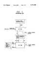
- a conventional font ROM control circuit for an on-screen display RAMincludes an address signal generation circuit 1 for outputting a readout address signal ADDR, an on-screen display RAM 2 for storing the character address CA and the character color data CCD of the record address signal ADDW and a record data DATA which are outputted from a central processing unit CPU and for outputting a character address signal CA and a character color data CCD in accordance with a readout address signal ADDR outputted from the address signal generation circuit 1, a column selection signal generation circuit 3 for outputting column selection signals CS1 through CSn in accordance with the character address signal CA outputted from the on-screen display RAM 2, a row selection signal generation circuit 4 for outputting row selection signals RS1 through RSn by counting a horizontal synchronous signal Hsync, and a font ROM 5 for storing the font data FD which is to be displayed and for outputting a font data FD in accordance with column selection signals CS1 through CSn outputted from the column selection signal generation circuit 3
- the character address which is to be displayed and the character color dataare outputted after the entire space of the on-screen display RAM 2 is selected using a readout address signal ADDR after recording a character address and a character color data.
- the central processing unit CPUoperates in accordance with a source program previously set in a ROM (not shown) and stores the character data into the on-screen display RAM 2. That is, when the recording data and a record address signal ADDW are outputted to the on-screen display RAM 2, the on-screen display RAM 2 stores the character address CA and the character color data CCD of the record data in accordance with a record address signal ADDW outputted from the central processing unit CPU.
- the on-screen display RAM 2outputs the character color data CCD and the character address CA to the output control circuit and the column selection signal generation circuit 3, respectively.
- the column selection signal generation circuit 3receives the character address CA and outputs the column selection signals CS1 through CSn to the font ROM 5, and the row selection signal generation circuit 4 counts the horizontal synchronous signal Hsync and outputs the row selection signals RS1 through RSn to the font ROM 5.
- the font ROM 5outputs the font data, which are selected by the column selection signals CS1 through CSn outputted from the column selection signal generation circuit 3 and by the row selection signals RS1 through RSn, to the output control circuit.
- the character color data CCD outputted from the on-screen display RAM 2 and the font data FD outputted from the font ROMare outputted to the CRT of a television through the output control circuit.
- the conventional font ROM control circuit for an on-screen displayhas disadvantages in that the capacity of a central processing unit should be big to meet an increasing capacity of an on-screen display RAM and the time and the entire applied program for recording the character data in an on-screen display as well as the capacity of a ROM should be big as the use of applied programs increase.
- It is another object of the present invention to provide an improved font ROM control circuit for an on-screen displaywhich includes an address signal generation circuit for outputting a readout address signal; an on-screen display RAM for storing a character address and a character color data of a character data in according to a record address signal outputted from a central processing unit and for outputting a previously stored character address and a character color data in accordance with a readout address signal; an address ROM for outputting character addresses and character color data in accordance with a readout address signal outputted from the address generation circuit; a memory selection register for outputting a memory selection signal so as to select a character address and for outputting a color memory selection signal so as to select a character color data; and a multiplexer for selecting character addresses and character color data outputted from the on-screen display ROM and the address ROM, respectively, in accordance with a memory selection signal and a character memory selection signal which are outputted from the memory selection register and for outputting the selected character addresses and character color data to a column selection signal
- FIG. 1is a block diagram of a conventional font ROM control circuit for an on-screen display.
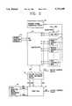
- FIG. 2is a block diagram of a font ROM control circuit for an on-screen display according to the present invention.
- FIG. 3is a view showing a memory selection register of FIG. 2 in detail.
- FIG. 4is a view showing a construction of a multiplexer of FIG. 2.
- a font ROM control circuit for an on-screen displayincludes an address signal generation circuit 10 for outputting an address signal to read out data, an on-screen display RAM 11 for storing a record address signal ADDW outputted from a central processing unit and for outputting a character color data CCDO) (shown as CO in FIGS. 2 and 4) and a character address CAO (shown as AO in FIGS. 2 and 4) in accordance with a readout address signal ADDR outputted from the address signal generation circuit 10, an address ROM 12 for storing a character address CA and a character color data CCD in a coded form and for outputting character addresses CA1 through CAn (shown as A1-An in FIGS.
- a memory selection register 13for outputting a character memory selection signal CMS to select a character color data CCD and a memory selection signal MS to select a character address CA
- a multiplexer 14for selecting a character address CAO outputted from the on-screen display RAM 11 and character addresses CA1 through CAn outputted from the address ROM 12 in accordance with a memory selection signal MS outputted from the memory selection register 13 and for outputting the selected signal to the column selection signal generation circuit 15, and for selecting a character color data CCDO outputted from the on-screen display RAM 11 and character color data CCD1 through CCDn outputted from the address ROM 12 in accordance with a character memory selection signal CMS outputted from the memory selection register 13 and for outputting the selected signals to the output control circuit, a column selection signal generation circuit 15 for outputting column selection signals CS1 through CSn in
- the address ROM 12includes ⁇ n ⁇ address ROMs 1 through n each storing a character address CA and a character color data CCD, in which an address ROM has the same number of the address as the memory size of the on-screen display RAM 11.
- the memory selection register 13includes 8-bit registers MS0 through MS6, CMS, of which the 8-bit register MS0 through MS6 have a memory selection signal MS for selecting a character address CA and the 8-bit register CMS has a character memory selection signal CMS for selecting a character color data CDD.
- the multiplexer 14includes a first multiplexer 144 for outputting character addresses CA0 through CAn in accordance with a memory selection signal MS outputted from the memory selection register 13, and a second multiplexer 145 for outputting character color data CCD0 through CCDn in accordance with a color memory selection signal CMS outputted from the memory selection register 13.
- a character address CA and a character color data CCDare stored in the ROM 12 in accordance with the source program.
- the central processing unit CPUoutputs a record address signal ADDW and a character data to the on-screen display RAM 11 and records a character address CA and a character color data CCD in the on-screen display RAM 11 in accordance with a record address signal ADDW.
- a readout address signal ADDRis outputted to the on-screen display RAM 11 and the address ROM 12, and the on-screen display RAM 11 outputs a character color data CCD0 and a character address CA0, and the address ROM 12 outputs character address CA1 through CAn and character color data CCD1 through CCDn to the multiplexer 14.
- a memory selection signal MS for selecting character addresses CA0 through CAn and a color memory selection signal CMS for selecting character color data CCA1 through CCDnare outputted to the multiplexer 14.
- the multiplexer 14outputs a character color data CCD and a character address CA to the output control circuit and the column selection signal generation circuit 15, respectively, which are selected by the memory selection signal MS and the character memory selection signal CMS outputted from the memory selection register 13 among the character addresses CA0 through CAn and the character color data CCD0 through CCDn outputted from the on-screen display RAM 11 and the address ROM 12, respectively.
- the column selection signal generation circuit 15receives the character address CA and outputs the column selection signals CS1 through CSn to the font ROM 17, and the row selection signal generation circuit 16 counts the horizontal synchronous signal Hsync and output the row selection signals RS1 through RSn to the font ROM 17.
- the font ROM 17stores the font data FD which is displayed in accordance with a program and outputs the font data FD selected by the column selection signals CS1 through CSn outputted from the column selection signal generation circuit 15 and the row selection signals RS1 through RSn outputted from the row selection signal generation circuit 16 to the output control circuit.
- the character color data CCD outputted from the multiplexer 14 and the font data FD outputted from the font ROM 17are combined by the output control circuit and are outputted to the CRT of the television.
- the font ROM control circuit for an on-screen displayis directed to provide an address ROM capable of recording data on and reading out from the on-screen RAM by providing a plurality of address ROMs in which a character address and character color data are stored in a coded form so as to implement one on-screen display to an address ROM, thereby to cope with an increasing needs of an on-screen display RAM having a large space.
Landscapes
- Engineering & Computer Science (AREA)
- Physics & Mathematics (AREA)
- Computer Hardware Design (AREA)
- General Physics & Mathematics (AREA)
- Theoretical Computer Science (AREA)
- Controls And Circuits For Display Device (AREA)
Abstract
Description
Claims (4)
Priority Applications (2)
| Application Number | Priority Date | Filing Date | Title |
|---|---|---|---|
| US08/495,876US5721568A (en) | 1995-06-28 | 1995-06-28 | Font ROM control circuit for on-screen display |
| JP7163428AJP2986716B2 (en) | 1995-06-28 | 1995-06-29 | Font ROM control circuit for on-screen display |
Applications Claiming Priority (2)
| Application Number | Priority Date | Filing Date | Title |
|---|---|---|---|
| US08/495,876US5721568A (en) | 1995-06-28 | 1995-06-28 | Font ROM control circuit for on-screen display |
| JP7163428AJP2986716B2 (en) | 1995-06-28 | 1995-06-29 | Font ROM control circuit for on-screen display |
Publications (1)
| Publication Number | Publication Date |
|---|---|
| US5721568Atrue US5721568A (en) | 1998-02-24 |
Family
ID=26488870
Family Applications (1)
| Application Number | Title | Priority Date | Filing Date |
|---|---|---|---|
| US08/495,876Expired - LifetimeUS5721568A (en) | 1995-06-28 | 1995-06-28 | Font ROM control circuit for on-screen display |
Country Status (2)
| Country | Link |
|---|---|
| US (1) | US5721568A (en) |
| JP (1) | JP2986716B2 (en) |
Cited By (7)
| Publication number | Priority date | Publication date | Assignee | Title |
|---|---|---|---|---|
| DE10129918A1 (en)* | 2001-06-21 | 2003-01-02 | Micronas Gmbh | Procedure for selecting pixel data |
| US20040165114A1 (en)* | 2003-01-09 | 2004-08-26 | Toshihiko Maruoka | On-screen display device |
| US20040233198A1 (en)* | 2003-03-05 | 2004-11-25 | Kabushiki Kaisha Toshiba | Font memory for display |
| US20050073523A1 (en)* | 2003-10-07 | 2005-04-07 | Canon Kabushiki Kaisha | Display unit, and apparatus having a display function |
| US20050174314A1 (en)* | 2004-02-06 | 2005-08-11 | Nec Electronics Corporation | Controller driver and display panel driving method |
| US20060039018A1 (en)* | 2004-08-23 | 2006-02-23 | Young-Chan Kim | Apparatus and method to provide OSD |
| US20070041404A1 (en)* | 2005-08-08 | 2007-02-22 | Ravi Palanki | Code division multiplexing in a single-carrier frequency division multiple access system |
Citations (6)
| Publication number | Priority date | Publication date | Assignee | Title |
|---|---|---|---|---|
| US4595996A (en)* | 1983-04-25 | 1986-06-17 | Sperry Corporation | Programmable video display character control circuit using multi-purpose RAM for display attributes, character generator, and refresh memory |
| US4737779A (en)* | 1983-08-29 | 1988-04-12 | Ing. C. Olivetti & C., S.P.A. | Data processing apparatus with dot character generator |
| US4864518A (en)* | 1986-09-04 | 1989-09-05 | Minolta Camera Kabushiki Kaisha | Proportional spacing display apparatus |
| US4954979A (en)* | 1985-08-22 | 1990-09-04 | Unisys Corporation | Personal computer with multiple independent CRT displays of ideographic and/or ASCII characters having loadable font memory for storing digital representations of subset or special characters |
| US5367317A (en)* | 1992-10-21 | 1994-11-22 | Mitsubishi Denki Kabushiki Kaisha | Screen display device |
| US5467109A (en)* | 1989-08-18 | 1995-11-14 | Nec Corporation | Circuit for generating data of a letter to be displayed on a screen |
Family Cites Families (3)
| Publication number | Priority date | Publication date | Assignee | Title |
|---|---|---|---|---|
| JPS5654484A (en)* | 1979-10-11 | 1981-05-14 | Nippon Electric Co | Character display unit |
| JPS5774781A (en)* | 1980-10-29 | 1982-05-11 | Ando Electric | Multiple division character indicating method |
| JPS5917585A (en)* | 1982-07-21 | 1984-01-28 | 株式会社日立製作所 | Character generator readout method |
- 1995
- 1995-06-28USUS08/495,876patent/US5721568A/ennot_activeExpired - Lifetime
- 1995-06-29JPJP7163428Apatent/JP2986716B2/ennot_activeExpired - Fee Related
Patent Citations (6)
| Publication number | Priority date | Publication date | Assignee | Title |
|---|---|---|---|---|
| US4595996A (en)* | 1983-04-25 | 1986-06-17 | Sperry Corporation | Programmable video display character control circuit using multi-purpose RAM for display attributes, character generator, and refresh memory |
| US4737779A (en)* | 1983-08-29 | 1988-04-12 | Ing. C. Olivetti & C., S.P.A. | Data processing apparatus with dot character generator |
| US4954979A (en)* | 1985-08-22 | 1990-09-04 | Unisys Corporation | Personal computer with multiple independent CRT displays of ideographic and/or ASCII characters having loadable font memory for storing digital representations of subset or special characters |
| US4864518A (en)* | 1986-09-04 | 1989-09-05 | Minolta Camera Kabushiki Kaisha | Proportional spacing display apparatus |
| US5467109A (en)* | 1989-08-18 | 1995-11-14 | Nec Corporation | Circuit for generating data of a letter to be displayed on a screen |
| US5367317A (en)* | 1992-10-21 | 1994-11-22 | Mitsubishi Denki Kabushiki Kaisha | Screen display device |
Cited By (12)
| Publication number | Priority date | Publication date | Assignee | Title |
|---|---|---|---|---|
| DE10129918A1 (en)* | 2001-06-21 | 2003-01-02 | Micronas Gmbh | Procedure for selecting pixel data |
| DE10129918B4 (en)* | 2001-06-21 | 2006-05-11 | Micronas Gmbh | Method for selecting pixel data |
| US20040165114A1 (en)* | 2003-01-09 | 2004-08-26 | Toshihiko Maruoka | On-screen display device |
| US7170564B2 (en)* | 2003-01-09 | 2007-01-30 | Matsushita Electric Industrial Co., Ltd. | On-screen display device |
| US20040233198A1 (en)* | 2003-03-05 | 2004-11-25 | Kabushiki Kaisha Toshiba | Font memory for display |
| US7218327B2 (en)* | 2003-03-05 | 2007-05-15 | Kabushiki Kaisha Toshiba | Font memory for a display |
| US20050073523A1 (en)* | 2003-10-07 | 2005-04-07 | Canon Kabushiki Kaisha | Display unit, and apparatus having a display function |
| US20050174314A1 (en)* | 2004-02-06 | 2005-08-11 | Nec Electronics Corporation | Controller driver and display panel driving method |
| US7495677B2 (en)* | 2004-02-06 | 2009-02-24 | Nec Electronics Corporation | Controller driver and display panel driving method |
| US20060039018A1 (en)* | 2004-08-23 | 2006-02-23 | Young-Chan Kim | Apparatus and method to provide OSD |
| EP1782178A4 (en)* | 2004-08-23 | 2009-07-22 | Samsung Electronics Co Ltd | METHOD AND APPARATUS FOR CREATING ON-SCREEN DISPLAY |
| US20070041404A1 (en)* | 2005-08-08 | 2007-02-22 | Ravi Palanki | Code division multiplexing in a single-carrier frequency division multiple access system |
Also Published As
| Publication number | Publication date |
|---|---|
| JPH0916151A (en) | 1997-01-17 |
| JP2986716B2 (en) | 1999-12-06 |
Similar Documents
| Publication | Publication Date | Title |
|---|---|---|
| US5129059A (en) | Graphics processor with staggered memory timing | |
| US4168488A (en) | Image rotation apparatus | |
| US4486856A (en) | Cache memory and control circuit | |
| JPS646477B2 (en) | ||
| US6195078B1 (en) | Parallel mode on-screen display system | |
| JPH0210434B2 (en) | ||
| EP0492840B1 (en) | Videographics display system | |
| US5721568A (en) | Font ROM control circuit for on-screen display | |
| US4933764A (en) | Improved teletext decoder which accommodates an increased number of character codes | |
| JP2697800B2 (en) | Display system | |
| US5107254A (en) | Address producing circuit for zoom function | |
| JPH06237422A (en) | Character display device | |
| EP0274439B1 (en) | Display system for plural display areas on one screen | |
| US4692759A (en) | Apparatus for modifying the appearance of the points of an image on the screen of a graphic image display console | |
| JPH0711915B2 (en) | Semiconductor memory device | |
| EP0420291B1 (en) | Display control device | |
| US6111615A (en) | Address generating and mapping device of video capture system | |
| US5812829A (en) | Image display control system and memory control capable of freely forming display images in various desired display modes | |
| EP0149511A2 (en) | Display memory circuit | |
| KR0148867B1 (en) | Font ROM Selection Circuit | |
| JPH0213317B2 (en) | ||
| KR960012690B1 (en) | Font-rom control circuit of osd | |
| JP2591064B2 (en) | Teletext broadcast receiver | |
| JPH0511475B2 (en) | ||
| JP2858831B2 (en) | Bitmap display method |
Legal Events
| Date | Code | Title | Description |
|---|---|---|---|
| AS | Assignment | Owner name:LG SEMICON CO., LTD., KOREA, REPUBLIC OF Free format text:ASSIGNMENT OF ASSIGNORS INTEREST;ASSIGNOR:KIM, HO HYUN;REEL/FRAME:007597/0091 Effective date:19950619 | |
| FEPP | Fee payment procedure | Free format text:PAYOR NUMBER ASSIGNED (ORIGINAL EVENT CODE: ASPN); ENTITY STATUS OF PATENT OWNER: LARGE ENTITY | |
| STCF | Information on status: patent grant | Free format text:PATENTED CASE | |
| FPAY | Fee payment | Year of fee payment:4 | |
| AS | Assignment | Owner name:HYNIX SEMICONDUCTOR INC., KOREA, REPUBLIC OF Free format text:CHANGE OF NAME;ASSIGNOR:LG SEMICON CO., LTD.;REEL/FRAME:015246/0634 Effective date:19990726 | |
| AS | Assignment | Owner name:MAGNACHIP SEMICONDUCTOR, LTD., KOREA, REPUBLIC OF Free format text:ASSIGNMENT OF ASSIGNORS INTEREST;ASSIGNOR:HYNIX SEMICONDUCTOR, INC.;REEL/FRAME:016216/0649 Effective date:20041004 | |
| FPAY | Fee payment | Year of fee payment:8 | |
| AS | Assignment | Owner name:U.S. BANK NATIONAL ASSOCIATION, AS COLLATERAL TRUS Free format text:AFTER-ACQUIRED INTELLECTUAL PROPERTY KUN-PLEDGE AGREEMENT;ASSIGNOR:MAGNACHIP SEMICONDUCTOR, LTD.;REEL/FRAME:022277/0133 Effective date:20090217 | |
| AS | Assignment | Owner name:HYUNDAI MICRO ELECTRONICS CO., LTD. (BRANCH OFFICE Free format text:CORRECTIVE ASSIGNMENT TO CORRECT THE RECEIVING PARTY DATA PREVIOUSLY RECORDED ON REEL 015246 FRAME 0634;ASSIGNOR:LG SEMICON CO., LTD.;REEL/FRAME:022703/0582 Effective date:19990726 | |
| AS | Assignment | Owner name:HYUNDAI ELECTRONICS INDUSTRIES CO., LTD., GEORGIA Free format text:MERGER;ASSIGNOR:HYUNDAI MICRO ELECTRONICS CO., LTD.;REEL/FRAME:022742/0478 Effective date:19991014 Owner name:HYNIX SEMICONDUCTOR INC., KOREA, REPUBLIC OF Free format text:CHANGE OF NAME;ASSIGNOR:HYUNDAI ELECTRONICS INDUSTRIES CO., LTD.;REEL/FRAME:022742/0555 Effective date:20010329 | |
| AS | Assignment | Owner name:HYUNDAI ELECTRONICS INDUSTRIES CO., LTD., KOREA, R Free format text:CORRECTIVE ASSIGNMENT TO CORRECT THE COUNTRY IN THE ADDRESS OF THE RECEIVING PARTY PREVIOUSLY RECORDED ON REEL 022742 FRAME 0478;ASSIGNOR:HYUNDAI MICRO ELECTRONICS CO., LTD.;REEL/FRAME:022746/0279 Effective date:19991014 | |
| AS | Assignment | Owner name:CROSSTEK CAPITAL, LLC, DELAWARE Free format text:ASSIGNMENT OF ASSIGNORS INTEREST;ASSIGNOR:MAGNACHIP SEMICONDUCTOR, LTD.;REEL/FRAME:022764/0270 Effective date:20090514 Owner name:CROSSTEK CAPITAL, LLC,DELAWARE Free format text:ASSIGNMENT OF ASSIGNORS INTEREST;ASSIGNOR:MAGNACHIP SEMICONDUCTOR, LTD.;REEL/FRAME:022764/0270 Effective date:20090514 | |
| AS | Assignment | Owner name:MAGNACHIP SEMICONDUCTOR, LTD., KOREA, REPUBLIC OF Free format text:PARTIAL RELEASE OF SECURITY INTEREST;ASSIGNOR:U.S. BANK NATIONAL ASSOCIATION, AS COLLATERAL TRUSTEE;REEL/FRAME:023075/0054 Effective date:20090527 Owner name:MAGNACHIP SEMICONDUCTOR, LTD.,KOREA, REPUBLIC OF Free format text:PARTIAL RELEASE OF SECURITY INTEREST;ASSIGNOR:U.S. BANK NATIONAL ASSOCIATION, AS COLLATERAL TRUSTEE;REEL/FRAME:023075/0054 Effective date:20090527 | |
| AS | Assignment | Owner name:YAT-SEN HOLDINGS, LLC, DELAWARE Free format text:ASSIGNMENT OF ASSIGNORS INTEREST;ASSIGNOR:CROSSTEK CAPITAL, LLC;REEL/FRAME:023094/0034 Effective date:20090812 | |
| FPAY | Fee payment | Year of fee payment:12 | |
| FEPP | Fee payment procedure | Free format text:PAYER NUMBER DE-ASSIGNED (ORIGINAL EVENT CODE: RMPN); ENTITY STATUS OF PATENT OWNER: LARGE ENTITY | |
| AS | Assignment | Owner name:INTELLECTUAL VENTURES II LLC, DELAWARE Free format text:MERGER;ASSIGNOR:YAT-SEN HOLDINGS, LLC;REEL/FRAME:025467/0090 Effective date:20101207 |