US5721430A - Passive and active infrared analysis gas sensors and applicable multichannel detector assembles - Google Patents
Passive and active infrared analysis gas sensors and applicable multichannel detector assemblesDownload PDFInfo
- Publication number
- US5721430A US5721430AUS08/583,993US58399396AUS5721430AUS 5721430 AUS5721430 AUS 5721430AUS 58399396 AUS58399396 AUS 58399396AUS 5721430 AUS5721430 AUS 5721430A
- Authority
- US
- United States
- Prior art keywords
- detector
- infrared
- substrate
- filter
- thermopile
- Prior art date
- Legal status (The legal status is an assumption and is not a legal conclusion. Google has not performed a legal analysis and makes no representation as to the accuracy of the status listed.)
- Expired - Fee Related
Links
Images


Classifications
- G—PHYSICS
- G01—MEASURING; TESTING
- G01N—INVESTIGATING OR ANALYSING MATERIALS BY DETERMINING THEIR CHEMICAL OR PHYSICAL PROPERTIES
- G01N21/00—Investigating or analysing materials by the use of optical means, i.e. using sub-millimetre waves, infrared, visible or ultraviolet light
- G01N21/17—Systems in which incident light is modified in accordance with the properties of the material investigated
- G01N21/59—Transmissivity
- G01N21/61—Non-dispersive gas analysers
- G—PHYSICS
- G01—MEASURING; TESTING
- G01N—INVESTIGATING OR ANALYSING MATERIALS BY DETERMINING THEIR CHEMICAL OR PHYSICAL PROPERTIES
- G01N21/00—Investigating or analysing materials by the use of optical means, i.e. using sub-millimetre waves, infrared, visible or ultraviolet light
- G01N21/17—Systems in which incident light is modified in accordance with the properties of the material investigated
- G01N21/25—Colour; Spectral properties, i.e. comparison of effect of material on the light at two or more different wavelengths or wavelength bands
- G01N21/31—Investigating relative effect of material at wavelengths characteristic of specific elements or molecules, e.g. atomic absorption spectrometry
- G01N21/35—Investigating relative effect of material at wavelengths characteristic of specific elements or molecules, e.g. atomic absorption spectrometry using infrared light
- G01N21/3504—Investigating relative effect of material at wavelengths characteristic of specific elements or molecules, e.g. atomic absorption spectrometry using infrared light for analysing gases, e.g. multi-gas analysis
- G01N21/3518—Devices using gas filter correlation techniques; Devices using gas pressure modulation techniques
- G—PHYSICS
- G01—MEASURING; TESTING
- G01N—INVESTIGATING OR ANALYSING MATERIALS BY DETERMINING THEIR CHEMICAL OR PHYSICAL PROPERTIES
- G01N21/00—Investigating or analysing materials by the use of optical means, i.e. using sub-millimetre waves, infrared, visible or ultraviolet light
- G01N21/17—Systems in which incident light is modified in accordance with the properties of the material investigated
- G01N21/25—Colour; Spectral properties, i.e. comparison of effect of material on the light at two or more different wavelengths or wavelength bands
- G01N21/31—Investigating relative effect of material at wavelengths characteristic of specific elements or molecules, e.g. atomic absorption spectrometry
- G01N21/35—Investigating relative effect of material at wavelengths characteristic of specific elements or molecules, e.g. atomic absorption spectrometry using infrared light
- G01N21/3504—Investigating relative effect of material at wavelengths characteristic of specific elements or molecules, e.g. atomic absorption spectrometry using infrared light for analysing gases, e.g. multi-gas analysis
Definitions
- the present inventiongenerally relates to the field of gas sensing devices. More particularly, the present invention relates to gas detectors capable of measuring the concentrations of one or more gases using a characteristic infrared absorption band of the gas to be detected.
- NDIRnondispersive infrared
- gas analyzersutilize the principle that various gases exhibit substantial absorption at characteristic wavelengths in the infrared radiation spectrum.
- a narrow-band optical or infrared transmission filteris used to isolate the wavelength band of interest in NDIR gas analyzers.
- a prism or diffraction gratingis used in gas analyzers relying on dispersive techniques.
- the NDIR techniquewhich is generally classified as a non-interactive gas analysis technique, offers a number of advantages over previous interactive types of gas measurement methods including electrochemical fuel cell, sintered semiconductor (tin dioxide), catalytic (platinum bead) and thermal conductivity. These advantages include speed of response, gas detection specificity, long term measurement stability, reduced maintenance, and greater specificity. Moreover, in some cases the interactive gas sensor can be poisoned into a nonfunctional state. Depending on the application, this could place human life at risk.
- Interactive gas sensorsare generally nonspecific because the reagent being used to determine the concentration of the desired gas may react with other gases that are present. This will naturally result in false readings. Further, if the equilibrium of the reaction between the nonspecific gas and the reagent is such that the gas and reagent remain reacted even after the partial pressure of the gas drops in the environment being monitored, the sensor will no longer function properly and is poisoned.
- the response time for NDIR gas sensorsis typically shorter than that for interactive gas sensors because the kinetics of the reaction between the sample gas and reagent controls how quickly the reactive type sensor can detect a change in the concentration of the gas in the environment being monitored.
- NDIR gas analyzershave not enjoyed wide spread application because of their complexity and high cost of implementation.
- NDIR gas analyzerstypically included an infrared source, a motor-driven mechanical chopper to modulate the source, a pump to push or pull gas through a sample chamber, a narrow bandpass interference filter, a sensitive infrared detector plus expensive infrared optics and windows to focus the infrared energy from the source onto the detector.
- the low-cost NDIR techniqueemploys a diffusion-type gas sample chamber of the type disclosed in U.S. Pat. No. 5,163,332, issued in Nov. 17, 1992, to the present applicant, and hereby incorporated by reference.
- This diffusion-type gas sample chambereliminates the need for: expensive optics, mechanical choppers, and a pump for pushing or pulling the gas into the sample chamber.
- a number of applications for the NDIR techniquewhich were previously considered impractical because of cost and complexity, have been opened.
- a goal of the present inventionis to further advance the technique of infrared gas analysis by providing a compact, reliable, low cost, and low power infrared gas sensor using infrared absorption.
- Another goal of the present inventionis to provide infrared detector assemblies which can be used in the infrared gas sensors according to the present invention.
- the present inventionis directed toward an infrared gas sensor for detecting the concentration of one or more predetermined gases using a novel infrared gas analysis technique referred to as passive infrared analysis (PIA).
- PIApassive infrared analysis
- the PIA technique of the present inventionis simpler than the NDIR gas analysis techniques known to date in that it does not require an "active" infrared source, nor does it require a structurally defined sample chamber.
- small, solid-state, low-cost and low power gas sensorscan be constructed to meet a host of special applications hitherto impossible using presently available NDIR gas analyzers.
- the present inventionrecognizes that all objects greater than 0 kelvin emit radiation.
- the present inventiontakes advantage of this fact by using ordinary objects, such as walls, ceilings, floors, etc. as a "passive" source of infrared radiation.
- These "passive" infrared radiation sourcescan be effectively used in some cases to replace the "active" infrared radiation sources that have been used almost exclusively hitherto in all NDIR gas analyzers.
- the "active" infrared source used in conventional NDIR gas sensorsis typically a heated and very hot object (500°-1000° C.) such as nichrome wire imbedded in alumina ceramic (Nerst glower) or a resistive tungsten wire of a small incandescent light bulb. These sources are characterized as “active” sources because they are powered by the gas sensor.
- a “passive” sourceis any object that is above 0 kelvin, but which is not powered by the gas detector power supply.
- Typical passive infrared sources that will be used by the infrared gas sensor of the present inventioninclude walls, carpets, tile floors, ceilings, and furnace walls to name just a few.
- the passive infrared sources which can be used by the gas sensor of the present inventionare virtually unlimited.
- the temperature of the passive infrared sourceshould be greater than the temperature of the gas to be measured. That is to say that the law of detailed balance must be observed.
- the temperature of active infrared sourcesis very high, the source area is typically quite small. A source area on the order of a few mm 2 is not uncommon.
- the temperature of typical indoor passive infrared sourceis only about 300K or -25° C., if the utilized source area is approximately 1000 times larger than that of conventional infrared sources, then using Planck's equation it can be shown that the spectral radiant emittance for the passive infrared source is comparable to that of conventional active sources in the spectral region from 3 to 20 microns.
- the passive infrared source area required for proper gas detectionwill depend on the temperature range expected from the passive infrared source.
- the passive infrared sourcemust be characterized.
- a detector assemblyis provided that is capable of measuring the spectral emittance from the selected passive infrared source at two different spectral bands.
- the spectral bands used for characterizing the sourceare preferably "neutral" spectral bands.
- Neutral spectral bandsare spectral bands which are chosen so that they are not absorbed, or only moderately absorbed, by any of the gases that are typically found in the environment to be monitored.
- the ratio of outputs measured at the two neutral spectral bandscan be used to uniquely determine the temperature of the passive infrared source assuming the two neutral spectral bands are close enough so that the variation of the emissivity function for the source is insignificant.
- the detector assemblyTo determine the concentration of the gas to be detected, the detector assembly also measures the amount of incident radiation at a "non-neutral" spectral band that coincides with an absorption band of the gas to be measured. This output, therefore, is indicative of the concentration of the gas within the angle subtended by the detector assembly to the passive infrared source.
- the concentration of the gas within the angle subtended by the detector assembly to the passive infrared sourcecan be determined.
- a passive source infrared gas detectorwhich uses an ambient temperature source, higher in temperature than the surrounding gas, and the space between the detector assembly and the source as the sample chamber.
- the gas detectorcomprises an infrared detector assembly for producing a first output, a second output, and a third output, the first output being indicative of the radiation received by the detector assembly at a first non-neutral spectral band which is absorbable by a preselected gas to be detected, the second output being indicative of the radiation received by the detector assembly at a first neutral spectral band from the passive infrared source, and the third output being indicative of the radiation received by the detector assembly at a second neutral spectral band from the passive infrared source.
- Signal processing meansare included for manipulating the three outputs to determine the concentration of the gas being monitored.
- the infrared gas detectorcan be used to monitor the concentration of a plurality of gases.
- a passive source infrared gas detectorwhich comprises:
- an infrared detector assemblycomprising
- a first sensor, a second sensor, and a third sensordisposed to receive radiation through the port for producing a first output, a second output, and a third output indicative of the radiation incident on the first sensor, second sensor, and third sensor, respectively,
- a first narrow bandpass filterinterposed between the port and the first sensor, the first narrow band bass filter producing an output therefrom indicative of the radiation incident on the first bandpass filter at a first non-neutral spectral band which is absorbable by a preselected gas to be detected
- a second narrow bandpass filterinterposed between the port and the second sensor, the second narrow bandpass filter producing an output therefrom indicative of the radiation incident on the second bandpass filter at a first neutral spectral band
- a third narrow bandpass filterinterposed between the port and the third sensor, the third narrow bandpass filter producing an output therefrom indicative of the radiation incident on the third bandpass filter at a second neutral spectral band
- thermo measuring meansfor producing an output corresponding to the ambient temperature of the first, second, and third sensors
- signal processing meansadapted to receive the outputs from the first sensor, second sensor, third sensor, and temperature measuring means and for sampling and at least temporarily storing the outputs of the first sensor, second sensor, third sensor, and temperature measuring means at preset intervals, the signal processing means including means for
- the infrared gas sensor according to the present inventionuses a passive infrared source in a novel PIA technique which effectively eliminates the need for a hot "active" infrared source that is used in conventional NDIR gas measurement devices. Furthermore, in the PIA technique employed in the infrared gas sensor of the present invention, the space between the passive infrared source, for example a certain portion of a wall, and the detector assembly becomes the sample chamber. In other words, the present invention not only eliminates the "active" infrared source, but it also eliminates the need for the sample chamber used in conventional NDIR gas analyzers.
- the power consumption of a infrared gas sensor according to the present inventioncan be significantly reduced, thus making the simple passive infrared gas sensor of the present invention battery operable for an extended period of time. Moreover, the size of the sensor can be reduced because a structurally defined gas chamber is no longer necessary.
- PDApassive infrared analysis
- a passive source infrared detector assemblycomprising: a detector housing having a port for receiving infrared radiation therethrough; a substrate mounted within the detector housing, the substrate having three apertures therein to transmit radiation entering the detector assembly therethrough; a first, a second and a third thermopile detector fabricated on the bottom side of the substrate, the hot junctions of each thermopile detector positioned over one of the apertures in the substrate so as to receive radiation transmitted through the aperture, and the cold junctions of each thermopile detector positioned over the substrate; a first interference bandpass filter mounted on the top side of the substrate so that the first filter covers the aperture above the first detector and the first filter is interposed between the port and the first detector, the first interference bandpass filter designed to pass incident radiation at a first non-neutral spectral band which is absorbable by a preselected gas to be monitored; a second interference bandpass filter mounted on the top side of the substrate so that the second filter covers the aperture above the second detector and the second filter is interposed between the port and
- an infrared detector assemblycomprising: a detector housing having a port for receiving infrared radiation therethrough; a substrate mounted within the detector housing, the substrate having three apertures therein to transmit radiation entering the detector assembly therethrough; a first, a second and a third thermopile detector fabricated on the bottom side of the substrate, the hot junctions of each thermopile detester positioned over one of the apertures in the substrate so as to receive radiation transmitted through the aperture, and the cold junctions of each thermopile detector positioned over the substrate; a first interference bandpass filter mounted on the top side of the substrate so that the first filter covers the aperture above the first detector and the first filter is interposed between the port and the first detector, the first interference bandpass filter designed to pass incident radiation at a first spectral band; a second interference bandpass filter
- an active infrared light sourcecan be operatively mounted within the detector assembly.
- the infrared detector assemblycan be used in NDIR applications employing an active source to detect up to as many gases as there are thermopile/filter combinations in the infrared detector assembly by appropriately selecting the spectral bands passed by the respective bandpass filters to pass wavelengths at which the desired gases to be detected strongly absorb infrared radiation. If fewer gases need be detected than the number of thermopile/filter combinations, the unneeded detector channels can be disabled.
- FIG. 1shows a preferred embodiment of the present invention depicting the detector assembly, the passive infrared source (wall) and the intervening space between the passive infrared source and the detector assembly constituting the sample chamber.
- FIG. 2is a graph showing the spectral radiant emittance of a black body at temperatures 100°-1,000° K.
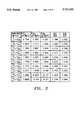
- FIG. 3is a table depicting the value of the ratio of the spectral radiant emittances for 0.1 micron spectral bands having center wavelengths of 5.00 and 3.91 microns as a function of the temperature of the "passive" infrared source.
- the emissivity values for both spectral bandsare assumed to be the same.
- FIG. 4is an exploded view of a detector assembly according to an embodiment of the present invention.
- FIG. 5is an oblique view showing a partial cutaway of the detector assembly illustrated in FIG. 4.
- FIG. 6shows an alternate preferred embodiment for the current invention depicting the actual use of a portion of a wall as the "passive" infrared source and the use of a convex spherical reflector to increase the original field of view (FOV) of the detector assembly.
- FOVfield of view
- FIG. 7shows a schematic drawing for the signal processing circuits for a preferred embodiment of the present invention.
- FIG. 8shows the circuit schematic for the signal processor according to another embodiment of the present invention.
- FIG. 9is a transverse cross sectional view taken along line 9--9 of FIG. 10 of another embodiment of a detector assembly according to the present invention.
- FIG. 10is a longitudinal cross sectional view of a detector assembly according to the embodiment in FIG. 9 taken along line 10--10.
- FIG. 11is an oblique view of the substrate and interference bandpass filters depicted in FIGS. 9 and 10.
- FIG. 12is a top view of the substrate used in the detector assembly embodiment illustrated in FIGS. 9 and 10.
- FIG. 13is an enlarged bottom view of the substrate used in the detector assembly embodiment illustrated in FIGS. 9 and 10 showing thermopiles manufactured thereon.
- FIG. 14is an illustration of a preferred construction of an interference bandpass filter for use in detector assemblies according to the present invention.
- FIG. 15is an illustration of a filter mounting fixture for use in detector assemblies according to the present invention.
- FIG. 16is a partial cross sectional view through the substrate illustrated in FIGS. 9-11 showing the filter mounting fixture of FIG. 15 in actual use.
- FIG. 17is an exploded view of a detector assembly according to another embodiment of the present invention.
- FIG. 18is an oblique view showing a partial cutaway of the detector assembly illustrated in FIG. 17.
- FIG. 19is a passive infrared analysis gas sensor according to another embodiment of the present invention.
- FIG. 20illustrates the detector assembly shown in FIGS. 17 and 18 in use in an NDIR gas sensor according to the present invention.
- FIG. 1depicts a detector assembly 3 comprising one signal detector 4 equipped with a narrow bandpass interference filter F 1 (not shown) whose center wavelength (CWL) L 1 coincides with the absorption band of the gas to be measured.
- detector assembly 3includes two source characterizing detectors 5 and 6 equipped respectively with narrow bandpass filters F 2 and F 3 (not shown) whose CWL's L 2 and L 3 , do not coincide with any known gases or vapors commonly found in the atmosphere.
- narrow bandpass filters F 2 and F 3not coincide with any known gases or vapors commonly found in the atmosphere.
- neutral wavelengthscan be found at 3.91 ⁇ m, 5.00 ⁇ m, and 9.00 ⁇ m.
- the CWL and the full width at half maximum (FWHM) values for the interference filter associated with detector 4are chosen to be 4.67 ⁇ m and 0.1 ⁇ m, respectively.
- the CWL and FWHM for the interference bandpass filter associated with detector 4are set at 4.26 and 0.1 ⁇ m, respectively.
- this techniquehas application to many other gases that have an absorption band in the infrared, including H 2 O and Total Volatile Organic Chemicals (TVOC's).
- the CWL L 1 of the interference filter F 1 associated with detector 4will be selected so that it falls as close as possible to the middle of the absorption band being used for the gas of interest. This will ensure that the maximum amount of radiation at the spectral band being monitored is absorbed by the gas, thus increasing the sensitivity and accuracy of the detector.
- gases which are very strong absorbers like CO 2it may be necessary to shift the CWL L 1 of the interference filter F 1 for detector 4 to ode side of the absorption band so that not as much light is absorbed at the spectral band being monitored. Such a shift should be considered when very long pathlengths are being used or when the concentration of the gas is very high. This technique can be used to prevent the detector from becoming starved for light within the range of gas concentrations to be monitored.
- the FWHM of interference filter F 1 associated with detector 4is preferably selected so that it is about 0.1 ⁇ m so that the detector has a high degree of specificity.
- other band widthsmay be selected depending on the width of the absorption band of the gas being monitored and the degree of specificity desired for the detector.
- L 2 and L 3 of the neutral spectral bands chosen for interference filters F 2 and F 3should be selected as close in spectral position as possible to L 1 . Although it is not necessary, it is also desirable for L 1 to fall between L 2 and L 3 .
- L 2 and L 3can be chosen to be 3.91 ⁇ m and 5.00 ⁇ m; respectively.
- L 2 and L 3can be chosen to be 3.91 ⁇ m and 9.00 ⁇ m.
- the FWHM of F 2 and F 3is preferably set at about 0.1 ⁇ m.
- the width of the spectral band passed by F 2 and F 3should be narrow enough that it does not overlap with an absorption line of a gas that would be found in the atmosphere.
- thermopile detectors 4are all preferably thermopile detectors. However, as those skilled in the art would recognize, other infrared detectors may be used in the present invention, including Platinum Silicide Schottky photodiodes.
- the field of view (FOV) of the detector assembly 3is determined by the aperture collar 7 attached to the detector assembly as shown in FIG. 1.
- the detector assembly 3subtends an area 8 (corresponding to area A) of the wall 9 which is used as the passive infrared source for the present invention.
- the effective sample path length S of the present infrared gas sensoris defined by the distance between the detector plane 10 of the detector assembly 3 and the wall 9.
- the sample path length S for the present inventionis, therefore, an extremely useful variable.
- the low concentration detection of a gas with an extremely weak absorption bandcan be accommodated by making the path length S very long (several meters) in order to attain adequate modulation for such a detection.
- the path length Sshould be set depending on the amount of modulation desired. For example, when a very strong absorber such as CO 2 is being monitored, shorter path lengths should be considered. However, if the desired application calls for detection of gas concentrations in the ppb range, then longer path lengths may be called for.
- path lengths between 5 inches and 10 feetwill typically be adequate, with most path lengths being between about 5 inches and 6 feet.
- the output V 1 of the signal detector 4is used to determine the concentration of the gas to be measured.
- the output V 1 of detector 4depends upon a number of factors. First and foremost, it is a function of the temperature T and the emissivity ⁇ of the passive infrared source 8 as governed by the spectral radiant emittance formula depicted in Equation 1! below. Furthermore, V 1 also depends upon system optical throughput, or attenuation, expressed as G (see Equation 1! below) and the concentration of the to-be-measured gas found between the detector assembly 3 and the passive infrared source 8. The concentration of the gas to-be-measured determines the value of the modulation factor M as shown in Equation 1! below.
- Detectors 5 and 6which are equipped with neutral filters F 2 and F 3 , are used to dynamically characterize the passive infrared source 8 and the environment in real time for the signal channel monitored by detector 4.
- the ratio Z of the outputs of detectors 5 and 6uniquely determines the temperature of source 8.
- the instantaneous values for the source emissivity ⁇ , system optical throughput (or attenuation) Gcan also be quickly determined using Equation 1! below and comparing the actual outputs with stored values of the respective outputs at the temperature T 0 and emissivity ⁇ 0 of a reference black body source measured while the system was initialized.
- the values for T, ⁇ and Gare continually updated in real time for the output of signal detector 4, enabling the latter to establish the concentration of the gas to be measured.
- the presently disclosed simple infrared gas sensoris also capable of rejecting the influence of stray radiation by virtue of the fact that the passive infrared source 8 is generally never a good reflector. Hence the amount of stray radiation that can find its way into the FOV of the optical system is minimal. Furthermore, unless the stray radiation happens to be in the spectral band defined by the filters of the detector assembly, namely L 2 and L 3 , they will be rejected. Even if they have energy within the spectral pass band of the sensor optical system, the emissivity is likely to be rather smooth and constant. In such a case, the neutral detectors will simply treat such stray radiation as an increase in the passive infrared source temperature 8 with the correct information related to the signal detector for proper processing.
- FIG. 2shows the spectral radiant emittance of a black body source at temperatures ranging from 100K to 1,000K.
- the infrared sourceis normally maintained at a constant and relatively high temperature (750-1,000K), and thus its spectral radiant emittance is typically represented by one of the curves above 700K in FIG. 2 dependent upon its absolute temperature.
- the present inventionrelies on infrared radiation from passive infrared sources.
- the black body curves around 300Kwill typically reflect the radiant emittance of the typical sources used with the present invention. Such is the case with the wall 9 in FIG. 1.
- the two narrow spectral bands 1 and 2 illustrated in FIG. 2are centered at 3.91 ⁇ m and at 5.00 ⁇ m, which, as discussed above, are desirable wavelength bands for neutral detectors 5 and 6 when monitoring CO or CO 2 . Because the bands illustrated in FIG. 2 correspond to the neutral spectral bands allowed to pass filters F 2 and F 3 , they would preferably have a FWHM of 0.1 ⁇ m.
- the ratio (Z) of the spectral radiant emittances at these two wavelength bandsuniquely determines the black body temperature.
- the only assumption made in this assertionis that the emissivity of the "passive" infrared source is approximately the same within the spectral band bounded by 3.91 ⁇ m and 5.00 ⁇ m. For almost all indoor walls which are either painted, wall-papered or wood-paneled, this is a good assumption.
- the passive source 8Before determining the concentration of the gas being monitored, the passive source 8 must be characterized.
- the manner whereby the detectors 5 and 6 dynamically characterize the temperature and the emissivity of the passive infrared source 8 for the signal channel 4is described as follows. For purposes of this discussion, detectors 4, 5, and 6 will be referenced as detectors D 1 , D 2 , and D 3 .
- R(T 0 , ⁇ 0 , L i )The Spectral Radiant Emittance of the passive infrared source (Watt cm -1 ⁇ -1 ), which is defined as ⁇ 0 ( ⁇ ) multiplied by the spectral radiant emittance of a black body as defined by Planck's Law as
- a 0Area of passive infrared source
- MModulation by the gas to be measured.
- the Planckian black body radiation physics together with the Wien's displacement lawstipulate that the ratio of the spectral radiant emittances at two spectral positions, when appropriately spaced, uniquely determines the temperature of a particular black body source in certain parts of the Planckian black body domain.
- the present inventiontakes advantage of this fact and recognizes that in the spectral regions between 3-15 microns and black body temperatures between 250-350K, such a ratio can indeed uniquely determine the temperature of the black body.
- the present value V 2 or V 3 of the respective neutral detector outputscan be used to deduce by calculations the changes (if any) for the other parameters, grouped together as a product, in Equation 1! above, namely the change in emissivity ⁇ of the passive infrared source 8 from ⁇ 0 , the change in the system optical throughput G and the change in the detector responsivity due to aging of the detector itself.
- the ratio of the outputs Z of these two detectorscan be used to characterize in real time the temperature of the passive infrared source 8. It is important to point out that since the changes in the other parameters in Equation 1! above, namely ⁇ , G and r are substantially the same for the two neutral detector channels, the value of the ratio Z, which is the only parameter needed to determine uniquely the temperature of passive infrared source 8, can always be obtained firsthand.
- the individual preset values of the signal and neutral detector outputs(V 10 , V 20 , V 30 , T 0 , and ⁇ 0 ) can be used to further assess, via calculations, any changes in the other parameters in Equation 1!. Since the parameters needed to determine the concentration of the gas to-be-measured from the signal channel detector output in Equation 1! are T, ⁇ , G, r and M, and since the first four parameters are dynamically characterized by the two neutral detector channels for the signal detector channel, the present invention, as illustrated in the present embodiment, is capable of accurately measuring the concentration of gas without the need for an active infrared source and the accompanying gas sample chamber.
- FIG. 3illustrates how the ratio of the spectral radiant emittances at 3.91 ⁇ m and 5.00 ⁇ m varies as a function of the passive infrared source temperature from 5° C. (278K) to 45° C. (318K).
- the emissivity ⁇is assumed to be 1 at both 3.91 ⁇ m and 5.00 ⁇ m.
- the curves themselvesare smooth and there is a very respectable difference in the value of the ratio as a function of the black body temperatures.
- Equation 1An example of how the concentration of the gas to-be-measured would be calculated from the outputs of V 1 , V 2 , and V 3 from detectors 4, 5, and 6 under a given set of circumstances using Equation 1! is now provided.
- the reference conditions for this exampleare defined as follows:
- T 0298° K or 25° C.
- the constantis the same for each detector channel and remains unchanged throughout the calculation in the present example, because a i is the same for each detector and the sample path length is set by design.
- the signal detector D 1has a CWL of 4.67 ⁇ m corresponding to the absorption band of carbon monoxide
- the neutral detector D 2has a CWL of 3.91 ⁇ m
- the neutral detector D 3has a CWL of 5.00 ⁇ m
- the measured voltage outputs from Detectors D 1 , D 2 and D 3 at initializationare as follows using Equation 1! and the table given in FIG. 3:
- V 105.4507 ⁇ 10 -5 A 0 r i CG 0 M volts
- V 201.7758 ⁇ 10 -5 YG 0 M volts
- V 307.6655 ⁇ 10 -5 YG 0 M volts
- the gas sensoris initialized by measuring the voltage outputs of each detector when no carbon monoxide is present and then when a known concentration of carbon monoxide gas is present within the field of view of the detector assembly. In this manner, a calibration curve for the gas sensor can be obtained as one skilled in the art would recognize.
- the sensoris ready to make real time measurements. For the present example, assume the following situation is encountered.
- the temperature of the passive infrared sourcehas increased to 308° K or 35° C. and the emissivity ⁇ of the passive infrared source 8 is 0.8.
- the optical attenuation factor Gis new 0.9; in other words there is now a 10% attenuation of the signal from the passive infrared source 8.
- the concentration of the carbon monoxide gas present within the field of view of the gas sensorcauses a 2% modulation in the signal detected by the signal detector D 1 .
- the modulation factor Mdecreases from 1.00 to 0.98 for the signal detector.
- the interference filters for the neutral channel detectorshave been appropriately selected to avoid the absorption bands of carbon monoxide and other gases which may be found in the environment being monitored.
- the table in FIG. 3was used to obtain the spectral radiant emittances for each of the wavelengths being monitored.
- the first step in determining the concentration of the carbon monoxide gas, or other gas to-be-measuredis to calculate the ratio Z of the outputs from the two reference detectors: ##EQU4##
- the temperature of the passive infrared source 8is determined to be 35° C. As stated above, it has been assumed that the area of the passive infrared source 8 and the optical arrangement remain unchanged during the example.
- the new voltage output for the neutral channel detector D 2should be the initiation value of 1.7758 ⁇ 10 -5 Y volts multiplied by the ratio (2.6517/1.7758), which equals 2.6517 ⁇ 10 -5 Y volts. Since the two voltages are not the same, it is known that the emissivity ⁇ or attenuation G or both are different than the initialization conditions.
- the product ⁇ Gcan be calculated as follows: ##EQU5## It should be noted that if the product of the emissivity ⁇ 0 and attenuation G 0 during initialization is less than 1.0, then the initialization value would need to be normalized to what it would be for an emissivity ⁇ 0 of 1.0 and an attenuation G 0 of 1.0. In this way, the ratio of the two voltage outputs will result in the product of the instantaneous value of the ⁇ G factor.
- the same informationcan also be deduced from using the output voltage from the other neutral detector monitoring the 5.00 ⁇ m channel.
- a corrected output voltage at the 4.67 ⁇ m, or signal, channelcan be calculated from the measured output of detector D 1 as follows:
- the output voltageis corrected for the ⁇ G factor and for temperature.
- the ratio of this corrected voltage output and the initiation voltage outputgives the modulation factor M as follows:
- the first step of the procedureis to obtain the temperature of the new passive infrared source 8 by calculating the ratio of the two reference detectors.
- the second stepis to compare the measured value for either of the two neutral channels with its initiation value and deduce the " ⁇ G" factor. Both of these pieces of information are then used to correct for the measured output from the signal detector D 1 at 4.67 microns. The ratio of this corrected value and stored initiation value for the signal detector D 1 will then yield the modulation factor.
- the modulation factoris used to give the concentrations of the gas present by using a calibration curve, which can be stored in the signal processing circuitry as is known in the art.
- the radiant emittance of the passive infrared sourceis a function of the area under the black body curves defined by Planck's Law multiplied by the emissivity ⁇ of the source, which will typically be the same for each of the neutral channels.
- the PIA gas sensor described in connection with FIGS. 1-3therefore, can alternatively be designed so that the FWHM of W 2 and W 3 of F 2 and F 3 (i.e., the neutral channels) are set so that their corresponding detectors measure the spectral radiant emittance from the passive infrared source 8 over a several micron band rather than the 0.1 ⁇ m band suggested above.
- the spectral bands passed by each of the neutral interference filterscan also overlap one another in such a system. The only limitations on such a configuration is that the two neutral detectors cannot measure the spectral radiant emittance for identical spectral bands and the emissivity ⁇ of the passive infrared source should be relatively constant over each of the spectral bands.
- the two neutral detectorscannot measure the spectral radiant emittance for identical spectral bands because the ratio Z would always be one in such situations.
- the emissivity ⁇ of the passive infrared sourceshould be relatively constant to ensure that this factor cancels out when calculating the ratio Z, thus enabling the temperature T of the passive infrared source to be determined directly from the ratio of the outputs from the two neutral channels.
- the FWHM W 2 of interference filter F 2can be set to pass light between 8 and 14 ⁇ m so that the detector 5 will measure the total amount of energy emitted by the passive source over this spectral band. If the spectral band passed by interference filter F 3 is narrower than that passed by F 2 then the ratio of the amount of energy detected by detectors 5 and 6 can still be used to uniquely determine the temperature of the passive infrared source 8 in real time as described above.
- Bandpass filter F 3preferably passes a spectral band of light that is approximately half the width that bandpass filter F 2 passes; thus, F 3 could be designed to pass the spectral radiant emittance from the passive infrared source falling within the range of 9.5 ⁇ m and 12.5 ⁇ m.
- the advantage of designing the neutral channels in this manneris that significantly more energy will be detected by detectors 5 and 6, respectively. This improves the signal to noise ratio for the detector, thereby permitting a more accurate characterization of the passive infrared source.
- the infrared gas detector according to FIG. 1can be used to monitor the concentration of a plurality of gases simply by adding additional detectors D i to the detector assembly 3 and appropriately selecting the CWL of interference filter F i to correspond to the characteristic absorption band of the gas desired to be monitored.
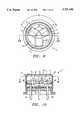
- FIGS. 4 and 5The construction of a detector assembly 3 according to one embodiment of the present invention is illustrated in FIGS. 4 and 5. As illustrated, the detector assembly is produced on a detector housing 31 such as a TO-5 can.
- the infrared detectors 4, 5 and 6are mounted on a housing base 30 of the TO-5 can 31. Infrared detectors 4, 5 and 6 are in close proximity to one another so that the field of view of each detector overlaps substantially with one another.
- detectors 4, 5 and 6are preferably thermopiles due to the fact that thermopiles do not require any power, have a linear output, and have a very good signal to noise ratio. Although not required, it is also preferable to tie the reference junctions of each of the three detectors to the same thermal heat sink.
- Filter mount 32is disposed on top of housing base 30 so that the only radiation which can enter the space between the filter mount 32 and housing base 30 is the radiation that enters through the three apertures 34 located in filter mount 32. Apertures 34 are located in filter mount 32 so that each aperture is in axial alignment with one of the detectors.
- Interference bandpass filters F 1 , F 2 and F 3cover apertures 34 so that they are interposed between the respective detector and the passive infrared light source. Furthermore, by covering the three apertures 34 located in filter mount 32 with interference filters F 1 , F 2 and F 3 , it is ensured that the only radiation that can enter the space between the filter mount 32 and the housing base 30 is that of the desired spectral bands. Divider 40 is used to prevent light of one spectral band from coming in contact with an infrared detector intended to measure light from a different spectral band.
- the CWL and FWHM of bandpass filters F 1 , F 2 and F 3are set as described in connection with FIGS. 1-3.
- the lid 42 to TO-5 can 31acts as aperture collar 7 and thus defines the FOV for the detector assembly 3.
- the top of lid 42comprises a light transmissive window 44.
- window 44is equally transmissive for each of the spectral bands being monitored. Window materials which have relatively uniform transmission qualities over the range of 1 ⁇ m to 10 ⁇ m include silicon, CaF 2 , and BaF 2 . CaF 2 and BaF 2 are particularly preferred materials because of their high transmissivity in this range.
- window 44may be eliminated altogether.
- the detector assembly 3 illustrated in FIGS. 4 and 5can be hermetically sealed and thus increase the life expectancy for the detector assembly. Further, as dust and grease build up on the detector assembly 3, the output signal corresponding to the spectral bands will begin to drop. If the attenuation of the signal becomes too large, the infrared gas detector will not function properly. However, by including window 44 in detector assembly 3, the original signal strength can be easily restored by cleaning window 44. This is not possible if window 44 is omitted.
- a TO-8 or larger packagecan be selected. For instance, such a platform might be used if the ability to monitor a plurality of gases is desired.
- detector assembly 3includes three infrared detectors 4, 5, and 6 that have been formed on substrate 50 mounted within detector housing 31.
- Detector housing 31is preferably a TO-5 can, comprised of a housing base 30, and a lid 42.
- Lid 42includes an aperture collar 7 which defines a port for receiving radiation into the detector assembly. The FOV of the detector assembly 3 is, therefore, limited by the aperture collar 7.
- Lid 42also preferably includes a light transmissive window 44 which fits within or covers the port defined by the aperture collar 7. Light transmissive window 44 is bonded to the lid 42 so that when lid 42 is attached to base 30, infrared detectors 4, 5, and 6 are hermetically sealed within detector assembly 3.
- Infrared detectors 4, 5, and 6are supported on a substrate 50 which, in the present embodiment, is made out of a semiconductor material such as Si, Ge, GaAs or the like. Because of their close proximity, the field of view of detectors 4, 5, and 6 overlap substantially.
- infrared detectors 4, 5, and 6are preferably thin film or silicon micromachined thermopiles.
- Thermopiles 4, 5, and 6each span an aperture 52 formed in the substrate 50.
- Apertures 52function as windows through which the radiation that is passed by bandpass filters F 1 , F 2 , and F 3 is detected.
- thin film or micromachined thermopile detectors 4, 5, and 6are manufactured on the bottom side of substrate 50 and may employ any of a number of suitable patterns.
- FIG. 13is an enlarged view of the bottom side of substrate 50 and illustrates one suitable pattern that could be employed for thin film or micromachined thermopile detectors 4, 5, and 6.
- a top view of substrate 50is provided in FIG. 12.
- thermopile detectors 4, 5, and 6are preferably supported on a thin electrically insulating diaphragm 54 that spans each of the apertures 52 formed in substrate 50 and the cold junctions 62 are positioned over the thick substrate 50. While the three apertures 52 are preferably spanned by a thin electrically insulating diaphragm 54, the thermopile detectors can also be self-supporting.
- infrared radiation from the passive infrared sourceenters the detector housing 31 through window 44.
- the infrared radiationthen strikes interference bandpass filters F 1 , F 2 , and F 3 , each of which passes radiation within a predefined spectral band.
- the radiation passing the interference filters F 1 , F 2 , and F 3then strikes the diaphragm 54, or hot junctions 60 if the thermopiles are self-supporting, where it is detected by infrared thermopile detectors 4, 5, and 6, respectively.
- the top side of the electrically insulating diaphragm 54can be coated with a thin film of bismuth oxide or carbon black during packaging so that the aperture areas absorb incident radiation more efficiently. If the thermopile detectors 4, 5, and 6 are self-supporting, then the side of hot junctions 60 upon which radiation is incident can be coated with bismuth oxide or carbon black directly.
- substrate 50acts as a heat sink to sustain the temperature of the cold junctions 62 of each of the detectors at a common temperature.
- substrate 50provides mechanical support to the device.
- thermopile detectors 4, 5 and 6formed thereon
- three separate substrates each having one infrared thermopile detector manufactured thereoncould be used in place of the substrate 50 described in the present embodiment.
- Electrically insulating diaphragm 54may be made from a number of suitable materials well known in the art, including a thin plastic film such as MYLAR®, which is a trademark for polyester film, or an inorganic dielectric layer such as silicon oxide, silicon nitride, or a multilayer structure comprised of both.
- a thin plastic filmsuch as MYLAR®, which is a trademark for polyester film
- an inorganic dielectric layersuch as silicon oxide, silicon nitride, or a multilayer structure comprised of both.
- the electrically insulating diaphragm 54is a thin inorganic dielectric layer because such layers can be easily fabricated using well known semiconductor manufacturing processes, and, as a result, more sensitive thermopile detectors can be fabricated on substrate 50. Moreover, the manufacturability of the entire device is improved significantly.
- substrate 50will have on-chip circuit capabilities characteristic of devices based on the full range of silicon integrated circuit technology; thus, the signal processing electronics for detectors 4, 5, and 6 can, if desired, be included on substrate 50.
- thermopile detectors 4, 5, and 6 on the bottom side of substrate 50are well known in the thermopile and infrared detector arts.
- One method suitable for producing thermopile detectors 4, 5, and 6 using semiconductor processing techniquesis disclosed in U.S. Pat. No. 5,100,479, issued Mar. 31, 1992, hereby incorporated by reference.
- output leads 56are connected to the output pads 64 of each of the thermopile detectors 4, 5, and 6 at bonding regions 58 using solder or other well known materials. Because the reference junctions of detectors 4, 5, and 6 are thermally shunted to one another, it is possible for the reference junctions for each of the detectors 4, 5, and 6 to share a common output pad. As a result, only four output leads would be required rather than six to communicate the output of the detectors.
- the output leads 56typically connect the detectors 4, 5, and 6 to signal processing electronics. As mentioned above, however, the signal processing electronics can be included directly on substrate 50 in which case output leads 56 would be connected to the input and output pads of the signal processing electronics, rather than the output pads from the infrared thermopile detectors 4, 5, and 6.
- a temperature sensing elementis preferably constructed on substrate 50 near cold junctions 62 of one of the thermopile detectors.
- the temperature sensing elementmonitors the temperature of substrate 50 in the area of the cold junctions and thus the temperature it measures is representative of the temperature of the cold junctions 62.
- the output from the temperature sensing element 53is communicated to the signal processing electronics so that the signal processing electronics can compensate for the influence of the ambient temperature of the cold junctions of the thermopile detectors.
- Temperature sensing element 53is preferably a thermistor, but other temperature sensing elements can also be used such as diodes, transistors, and the like.
- interference bandpass filters F 1 , F 2 , and F 3are mounted on the top of substrate 50 so that they each cover one of the apertures 52 in substrate 50.
- the CWL and FWHM of bandpass filters F 1 , F 2 , and F 3are set as described in connection with FIGS. 1-3 above. Because the interference filters cover apertures 52, light entering detector assembly 3 through window 44 must first pass through filter F 1 , F 2 , or F 3 before reaching infrared detector 4, 5, or 6, respectively.
- infrared detector 45, or 6, respectively.
- the light passing through one of the filtersis isolated from the light passing through one of the other filters. This prevents cross talk between each of the detector channels. Therefore, the light that reaches infrared detectors 4, 5, and 6 from the passive infrared source 8 is the light falling within the spectral band intended to be measured by the particular detector.
- the filters F 1 , F 2 , and F 3are secured to substrate 50 using a thermally conductive material, such as thermally conductive epoxy.
- a thermally conductive materialsuch as thermally conductive epoxy.
- interference bandpass filters F 1 , F 2 , and F 3are each above 0K they give off a certain amount of infrared radiation.
- the total radiant flux incident at a detector due to its filter, which normally has a temperature close to that of ambient,is a function of how well the filter is thermally shunted to the reference or cold junctions 62 of the detector.
- a thermopileis nothing more than a large number of thermocouples wired in series to increase the output voltage of the device. Thus, how well a filter is thermally shunted to the reference junctions of its thermopile detector can effect the output voltage of the detector.
- the radiant flux incident at the thermopile detectorincludes an undesirable bias from the filter that diminishes the modulation of the desired signal from the passive infrared source 8 that passes through the filter from the outside to the hot junctions of the thermopile.
- the ratio of the useable to the non-useable signal at the hot junctionsis given by the ratio of the spectral radiant emittance of the passive infrared source 8 at the spectral band passed by the interference filter to the spectral radiant emittances given off by the filter at all wavelengths.
- the filteris always somewhat shunted to the reference electrode of the thermopile detector and the ratio of useable signal to the non-useable signal is around 0.1 to 0.2.
- the present detector assembly embodimentspecifically eliminates, as much as possible, the unwanted radiant flux coming at the thermopile detector from the filter. This is done by providing a very efficient thermal shunt between the reference (cold) junctions 62 of the thermopile detectors 4, 5, and 6 and their corresponding interference filters F 1 , F 2 , and F 3 . This in effect nulls out the influence of the filter to the signal (hot) junctions 60 of the detector, thus rendering the radiation passed by the filters from the passive infrared source 8 the only source of the radiation that is measured by the thermopile detectors. Needless to say, this is the only radiation that is important, and it is now usefully isolated for processing by the thermopile detector.
- a heat sinking metallic grid 68can be deposited on one or both sides of the interference filters F i as shown in FIG. 14.
- the metal used for the gridshould have a high thermal conductivity. Gold is particularly well suited for this purpose.
- a heat sinking metallic grid 68can be incorporated into a mounting fixture 70. The thermal conductivity of metallic grid 68 can be improved by coating the grid with gold.
- Mounting fixture 70comprises a grid portion 68 and a raised lip portion 72.
- Interference filter F i(corresponding to filters F 1 , F 2 , or F 3 ) sits in the recess formed by the raised lip 72.
- filter F iis preferably bonded to mounting fixture 70 using a thermally conductive material, such as thermally conductive epoxy.
- the mounting fixtureis then bonded, using a thermally conductive material, to the top of substrate 50 to cover aperture 52.
- FIG. 16is a partial cross sectional view through substrate 50 at one of the thermopile detectors D i corresponding to detectors 4, 5, or 6.
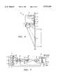
- Detector assembly 79includes three infrared detectors 4, 5, and 6 (not shown) formed on semiconductor substrate 80 mounted within detector housing 31.
- Infrared detectors 4, 5, and 6are thin film or micromachined infrared thermopile detectors formed on the bottom side of substrate 80 as described in connection with the detector assembly embodiment illustrated in FIGS. 9-13.
- substrate 80 of the present embodiment and substrate 50 of the embodiment illustrated in FIGS. 9-13is that substrate 80 includes a raised rim 82 surrounding each of the three apertures 52 formed in the substrate. Raised rims 82 provide additional thermal mass to maintain the temperature of the reference (cold) junctions of the thermopiles 4, 5, and 6 at the same temperature.
- the added thermal massis desirable in the present embodiment, because the detector assembly 79 according to the present embodiment also includes an active infrared light source 84 operatively mounted within the detector housing 31.
- a temperature sensing element 53(not shown) is preferably constructed on substrate 50 near the cold junctions of one of the thermopile detectors in order to monitor the temperature of the cold junctions and provide that information to the signal processing electronics.
- Infrared light source 84provides added flexibility to detector assembly 79. Namely, it permits the three channel detector assembly 79 to be used in a traditional NDIR gas sensor having an active infrared light source, or, alternatively, if infrared light source 84 is disabled, detector assembly 79 can be used in a passive infrared gas sensor according to the present invention.
- detector assembly 79is used in an NDIR gas sensor the added thermal mass provided by the raised rims 82 helps maintain the temperature of the reference junctions at as uniform of temperature as possible when the active infrared light source 84 is cycling on and off. This is helpful in maintaining the sensitivity of the detectors to the modulation in their signal due to the presence of a gas, or gases, being monitored in the sample path of the detectors.
- Detector housing 31 in the present embodimentis a TO-5 can, comprised of a housing base 30, and a lid 42.
- Lid 42includes an aperture collar 7 which defines a port for receiving radiation into the detector assembly. The FOV of the detector assembly 79 is limited by the aperture collar 7. Because of their close proximity, the FOV of detectors 4, 5, and 6 overlap substantially.
- Lid 42also preferably includes a light transmissive window 44 which fits within or covers the port defined by the aperture collar 7. Light transmissive window 44 is bonded to the lid 42 so that when lid 42 is attached to base 30, infrared detectors 4, 5, and 6 are hermetically sealed within detector housing 31.
- the material used for window 44should be selected as described in connection with the detector assembly embodiments illustrated in FIGS. 4 and 5 and 9-16.
- Interference bandpass filters F 1 , F 2 , and F 3are mounted on the top of raised rims 82 so that they each cover one of the apertures 52 in substrate 80.
- the CWL and FWHM of bandpass filters F 1 , F 2 , and F 3are set as described in connection with FIGS. 1-3 above. Because the interference filters cover apertures 52, light entering detector housing 31 through window 44 must first pass through filter F 1 , F 2 , or F 3 before reaching infrared detector 4, 5, or 6, respectively.
- filter F 1 , F 2 , or F 3must first pass through filter F 1 , F 2 , or F 3 before reaching infrared detector 4, 5, or 6, respectively.
- the light that reaches infrared detectors 4, 5, and 6 from the passive infrared source 8--or from the active infrared source 84 if the detector assembly is being used in a conventional NDIR gas sensor--is the light falling within the spectral band intended to be measured by the particular detector.
- Interference bandpass filters F 1 , F 2 , and F 3are bonded to the top of raised rims 82 surrounding apertures 52 using a thermally conductive material, such as thermally conductive epoxy.
- a thermally conductive materialsuch as thermally conductive epoxy.
- a heat sinking metallic grid 68can be deposited on one or both sides of the interference filters F i as shown in FIG. 14.
- the metal used for the gridshould have a high thermal conductivity. Gold is particularly well suited for this purpose.
- a heat sinking metallic grid 68can be incorporated into a filter mounting fixture 70.
- Mounting fixture 70comprises a grid portion 68 and a raised lip portion 72.
- an interference filter F i(corresponding to filters F 1 , F 2 , and F 3 ) sits in the recess formed by the raised lip 72.
- filter F iis preferably bonded to mounting fixture 70 using a thermally conductive material, such as thermally conductive epoxy.
- the mounting fixtureis then bonded, using a thermally conductive material, to the top of one of the raised rims 72 to cover aperture 52.
- Substrate mounting fixtures 86are connected to the output pads (not shown) of each of the thermopile detectors 4, 5, and 6 at bonding regions 88 using solder or other well known materials. As the reference junctions of the detectors 4, 5, and 6 share a common output pad in the present embodiment, only four substrate mounting fixtures 86 are required to communicate the outputs of the detectors. Substrate mounting fixtures 86 are insulated from the base 30 of detector housing 31 because they are mounted on an electrically insulative substrate 90, which is preferably made out of a material selected from the group consisting of aluminum oxide and beryllium oxide. The output signal from detectors 4, 5, and 6 is communicated through substrate mounting fixtures 86, via wire bonds 94, to the signal processing electronics 92. Signal processing electronics 92 can comprise a plurality of microchips diebonded to insulative substrate 90 or a single microchip diebonded to insulative substrate 90. Output leads 56 are connected to the input and output of the signal processing electronics 92 via wire bonds 96.
- Signal processing electronics 92includes a source driver 98 for driving active infrared source 84 at a known frequency.
- Source driver 98drives active infrared source 84 through wire bonds 97.
- the manner in which active infrared source 84 should be driven by source driver 98 for conventional NDIR applicationsis well known in the art and need not be explained further herein.
- detector assembly 79has been illustrated as including signal processing electronics 92 diebonded on insulative substrate 90, signal processing electronics 92 could be incorporated directly on semiconductor substrate 80.
- output leads 56could be connected directly to the outputs of detectors 4, 5, and 6 using solder or other well known materials. The output leads 56 would, in this situation, connect the outputs of infrared thermopile detectors 4, 5, and 6 to signal processing circuitry on the exterior to the detector assembly 79.
- infrared radiation from the passive infrared source 8enters the detector housing 31 through window 44.
- the infrared radiationthen strikes interference bandpass filters F 1 , F 2 , and F 3 , each of which passes radiation within a predefined spectral band.
- the radiation passing the interference filters F 1 , F 2 , and F 3then strikes the inorganic dielectric membrane (not shown) spanning each of the apertures, or hot junctions if the thermopiles are self-supporting, where it is detected by infrared thermopile detectors 4, 5, and 6, respectively.
- the outputs from each of the detectorsis then communicated to the signal processing electronics where it is processed in accordance with the description of the passive infrared gas sensor provided above in connection with FIGS. 1-3.
- the sensitivity of detectors 4, 5, and 6 to incident radiationcan be improved by coating the top side of the dielectric membrane (not shown) with a thin film of bismuth oxide or carbon black during packaging so that the aperture areas absorb incident radiation more efficiently. If the thermopile detectors 4, 5, and 6 are self-supporting, then the side of the hot junctions upon which radiation is incident can be coated with bismuth oxide or carbon black directly.
- detector assembly 79also includes an active passive infrared source, it can be utilized in an NDIR gas sensor.
- detector assembly 79in an NDIR gas sensor according to the present invention is described in detail below.
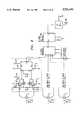
- FIG. 6shows the actual implementation of a preferred embodiment of a PIA gas sensor 33 according to the present invention.
- the detector assembly 3is mounted directly on the printed circuit board (PCB) 11 which also is a mount for the signal processing electronics 12, siren 13 for sounding an alarm and a battery power source 14.
- Battery power source 14is preferably a lithium battery, which should provide sufficient power to operate the system from 1 to 2 years.
- the present PIA gas sensoris illustrated as employing detector assembly 3, detector assembly 79 described in connection with FIGS. 17 and 18 can also be employed in the present embodiment.
- Spherical reflector 15which is affixed rigidly to the detector assembly 3, is used to increase the FOV of the detector assembly 3.
- the sample path length for the gas sensor in this caseis again defined by the distance between the detector assembly 3 and the passive infrared source 8, which is defined as a portion of the wall 9.
- the PCB 11 carrying all the components described earlieris housed in an enclosure 16 for protection from handling and external environments when being used to implement the PIA technique of the present invention.
- the FOV of detector assembly 3can similarly be enhanced by using a refractive optics system instead of reflective optics system. Reflective optics are preferred, however, because of their cost.
- FIG. 7shows the schematic drawing for the signal processing circuits according to a preferred embodiment for the present invention.
- the signal processing circuits illustrated in FIG. 7can be used in conjunction with any of the detector assembly embodiments described above.
- thermopile detectorsare thermopile detectors and their reference junctions are tied thermally to the same heat sink 20.
- One of the major advantages of the thermopile detectorsis their linear output (scalable linearly with temperature from 0° to 70° C.).
- the outputs of the detectors 17, 18 and 19can be corrected for environmental temperature changes by sensing the same at the common reference junction heat sink 20 using microprocessor 21.
- detector assembly 3Although the present embodiment is illustrated as employing detector assembly 3, detector assembly 79 described in connection with FIGS. 17 and 18 can also be employed in the present embodiment.
- each of the three detectors outputsare subsequently switched with the same duty factor by a low noise multiplexer 22 controlled by the microprocessor 21 to the differential input of the same low noise preamplifier 23.
- the amplified signalsare then converted by an A/D converter 24 before being fed into the microprocessor 21 for signal processing.
- the concentration of the gascan be monitored based on a predetermined function programmed into microprocessor 21. The concentration can be outputted or displayed using cable 25 or in some cases an alarm signal can also be generated by the microprocessor 21 using cable 26.
- Microprocessor 21is of the low power type and contains enough RAM, ROM and EEprom for appropriately processing the signals originated by the detector assembly 3.
- the versatility of the passive infrared gas detectors of the present inventioncould be further enhanced by adding a distance measuring device to the gas detector.
- the distance measuring devicecould be of the contact or non-contact type.
- itcould comprise a laser diode with a sensor as is well known in the art.
- the output of the distance measuring devicewould be communicated to the signal processor so that the appropriate sample path length S can be inserted into Equation 1! when calculating the concentration of the gas.
- the change in the path lengthis not required for calculating the ratio of the outputs from the two neutral channels, because this factor would cancel out since it would be the same for both detectors.
- the gas detectorcan include a switch so that the user can enter preset pathlengths.
- the switchmight include path length settings increasing by one foot increments so that the user can measure and enter the appropriate path length for the set up in which the gas detector of the present invention is being used.
- the selection of a particular path lengthis communicated to the microprocessor 21 so that it knows the appropriate path length to use in calculating the concentration of the gas in the sample volume.
- a data entry padcan be used so that the user can enter any desired path length and the microprocessor 21 will compensate accordingly during its calculations.
- FIG. 8is a circuit schematic for a signal processor according to another embodiment of the present invention.
- the structure of the circuitis determined by the low level of the expected signals, in the order of 5 to 85 ⁇ Volt.
- the amplifiersare constructed in the form of instrumentation, amplifiers which have a very high common mode signal rejection, because for operation in the home near 60 Hz power wiring large signals may be induced magnetically. Magnetic shielding of the detectors and circuits should reduce this.
- the detectors and circuit componentsshould also be protected from rapid temperature changes which can produce thermocouple signals in the components.
- the thermal and mechanical designare very important to allow the full capabilities of the electronic circuit.
- U1forms the input part of the instrumentation amplifier. It was selected for its very low input offset voltage, about 0.5 ⁇ V, and very low change of that voltage with temperature.
- the two feedback resistors R2 and R3should be matched to better than 0.1%, and should have temperature coefficients of 10 ppm/deg C. or better.
- the gain of this circuitis determined by the ratio of R2 and R3 to R1, about 500.
- the noise level for dc to 10 Hzis about 2 ⁇ V pp. This is higher than is desirable, but it can be filtered later.
- the low input offset and drift with temperatureare more important to obtain proper processing of the sampled outputs.
- the input noise level of the output part of the circuitis much lower, about 0.28 ⁇ V, but the offset is much higher, about 50 uV, and with a larger temperature coefficient.
- U2is actually another instrumentation amplifier. It is used to provide a stable high gain of about 400. It is used because it is less expensive than another amplifier and four accurate gain setting resistors.
- the expected outputis from one to two volts or more, depending on the input radiation to the detector. The gains of the preamps for the other two detectors are lower since more radiation is expected at the longer wavelengths of those detectors.
- the rest of the signal processingcould be handled in many different ways, one implementation is shown as an example.
- the three signal channels and one temperature sensor near the detectorsare selected by a multiplexer, and their value converted to a frequency by a voltage to frequency converter.
- the frequency outputcan be processed easily by a microprocessor ( ⁇ P), to determine the temperature of the scene viewed, the temperature of the detectors, and then the absorption due to CO gas, or other gas to be measured, from the expected signals at those temperatures.
- ⁇ Pmicroprocessor
- Passive infrared gas sensor 110 illustrated in FIG. 19comprises a passive infrared source 112, a three channel infrared detector assembly 3 centered in the middle of passive infrared source 112 and having a port 118 for receiving infrared radiation therethrough, and a concave mirror 120 spaced apart from and facing the port 118 of the detector assembly 3 and the passive infrared source 112.
- Passive infrared source 112is preferably concave to increase the surface area of the infrared source within the field of view of the concave mirror 120 facing the passive infrared source.
- passive infrared source 112comprises an infrared black surface 116 that has been applied to the surface of a nonconductive member 114.
- Infrared black surface 116can comprise a number of materials, including black chrome oxide, bismuth oxide and carbon black.
- Nonconductive member 114is comprised out of a plurality of plastic panels due to the light weight and ease of manufacture associated with plastic. As would be obvious to those skilled in the art, member 114 could also be made out of a unitary piece of plastic or other electrically insulative material.
- Mirror 120can be any concave reflective surface so as to increase the field of view of the detector assembly.
- concave mirror 120has as low of an emissivity as possible, so that all of the infrared radiation being received through port 118 in detector assembly 3 is produced by the passive infrared source 112.
- the passive infrared source 112should be large enough to fill the field of view of the concave mirror.
- the space between the passive infrared source and detector on one hand and the concave mirror on the other handdefines the sample chamber of the passive infrared gas sensor 110 according to the present invention.
- Infrared radiation emitted by the passive infrared source 112is reflected off concave mirror 120 into detector assembly 120 through port 118.
- the sample path length of the passive infrared gas sensor 110is at least twice the distance between the detector assembly 3 and the concave mirror 120. This permits the gas sensor 110 to have twice the sensitivity of passive infrared gas sensor in which the passive source is opposing the detector assembly.
- gas sensor 110can have the same sensitivity using half the space.
- detector assembly 79 described in connection with FIGS. 17 and 18also includes an active infrared source; thus, detector assembly 79 can be directly employed in an NDIR gas sensor.
- One potential NDIR gas sensor arrangement according to the present inventionis illustrated in FIG. 20.
- the NDIR gas sensor of FIG. 20comprises an elongated hollow tube 100 having a closed end 102 and an open end 104.
- the tube 100is composed of a metal and has a circular cross section. In other embodiments, the cross section is square.
- Inner surfaces of tube 100, including the inner surface of closed end 102,are specularly reflective.
- the metal tube 100is gastight and therefore filtering apertures, of which the filtering aperture 106 is typical, are provided at spaced locations along the tube 100 to permit the gas being monitored to enter and to leave the space within the tube.
- Each of the filtering apertures 106is covered by a semipermeable membrane 108.
- the exact number, location, and disposition of the filtering aperturesis not crucial, although some arrangements may be more optimal than others.
- Three channel detector assembly 79is mounted in the open end of hollow tube 100 in such a manner as to close off the open end and prevent gas from entering or exiting through the open end of tube 100. Because the active infrared source 84 is utilized in the present invention, detectors 5 and 6, which are used as neutral detectors to characterize the temperature of the passive infrared source 8 when the detector assembly 79 is used in a passive infrared gas sensor according to the present invention, are not required.
- detector assembly 79can be used to monitor the concentration of up to three different gases in the present embodiment by simply selecting bandpass filters F 1 , F 2 , and F 3 that pass spectral bands at three different wavelengths at which three different gases to be detected strongly absorb radiation and at which other gases that might be present do not absorb. If fewer than three gases need be detected, the unneeded detector channels can be disabled. This adds a great deal of flexibility to the NDIR gas sensor according to the present invention.
- the concentration of the gases to be detected within the sample chamberis determined by the extent to which they absorb radiation emitted from the active infrared source 84.
- detector assembly 79By inserting detector assembly 79 into the open end of tube 100 window first as illustrated in FIG. 19, detectors 4, 5, and 6, interference bandpass filters F 1 , F 2 , and F 3 , and active infrared source 84 located within detector assembly 79 are arranged so that they are all facing the inner surface of closed end 102.
- some of the radiation emitted by active infrared source 84is reflected, either directly or indirectly, from the inner surface of the closed end 102 back to the detectors 4, 5, and 6 where it is detected.
- the amount of radiation detected at the spectral bands monitored by detectors 4, 5, and 6can then be used to determine the concentration of the gases being monitored within the sample chamber defined by the space within tube 100 using techniques well known in the art.
- the purpose of the semipermeable membrane 108is to prevent airborne particles larger than a predetermined size from entering the space within the tube 100, while at the same time not interfering appreciably with the free diffusion of the gas to be monitored into and out of the space within the tube 100.
- the unwanted particlesinclude minute droplets of moisture or oil and also include fine particulate matter such as particles of dust or smoke. If these unwanted airborne particles were to enter the space within the tube 100, they would deposit themselves onto the specularly reflective surfaces thereby reducing the reflectivity and destroying its specular nature. The unwanted particles would also deposit onto the window 44 of detector assembly 79 reducing the transmission of radiation. All of these problems are eliminated through the use of the semipermeable membrane which, in the preferred embodiment prevents airborne particles larger than 0.3 microns from entering the space within tube 100.
Landscapes
- Physics & Mathematics (AREA)
- Spectroscopy & Molecular Physics (AREA)
- Health & Medical Sciences (AREA)
- Life Sciences & Earth Sciences (AREA)
- Chemical & Material Sciences (AREA)
- Analytical Chemistry (AREA)
- Biochemistry (AREA)
- General Health & Medical Sciences (AREA)
- General Physics & Mathematics (AREA)
- Immunology (AREA)
- Pathology (AREA)
- Investigating Or Analysing Materials By Optical Means (AREA)
- Spectrometry And Color Measurement (AREA)
- Photometry And Measurement Of Optical Pulse Characteristics (AREA)
Abstract
Description
Sample Path length S= A/OM!*
V.sub.10 =R(T.sub.0, ε.sub.0, L.sub.i)A.sub.0 W.sub.i r.sub.i (a.sub.i /(2πS.sup.2))GM volts Equation 1!
i=1, 2 or 3;
(2πhc.sup.2 λ.sup.-5)/(exp(ch/k.sub.B λT)-1);
V.sub.i =R(T, ε, L.sub.i)AW.sub.i r.sub.i (a.sub.i /(2πS.sup.2))GM volts
5.3802×10.sup.-5 Y volts (5.4507/7.6250)×(1/0.72) =5.3417×10.sup.-5 Y volts
5.3417×10.sup.-5 Y/5.4507×10.sup.-5 Y=0.98.
Claims (38)
Priority Applications (9)
| Application Number | Priority Date | Filing Date | Title |
|---|---|---|---|
| US08/583,993US5721430A (en) | 1995-04-13 | 1996-01-10 | Passive and active infrared analysis gas sensors and applicable multichannel detector assembles |
| BR9612406-7ABR9612406A (en) | 1996-01-10 | 1996-12-26 | Passive infrared analysis gas sensors and applicable multi-channel detector mounts |
| KR1019980705299AKR19990077161A (en) | 1996-01-10 | 1996-12-26 | Passive infrared analysis gas sensor and its multichannel detector assembly |
| AU14314/97AAU1431497A (en) | 1996-01-10 | 1996-12-26 | Passive infrared analysis gas sensors and applicable multichannel detector assemblies |
| CN96199608ACN1216108A (en) | 1996-01-10 | 1996-12-26 | Passive infrared analysis gas sensors and applicable multichannel detector assemblies |
| JP09525251AJP2000503122A (en) | 1996-01-10 | 1996-12-26 | Passive infrared analysis gas sensor and multi-channel detector using it |
| PCT/US1996/020796WO1997025613A1 (en) | 1996-01-10 | 1996-12-26 | Passive infrared analysis gas sensors and applicable multichannel detector assemblies |
| CA002242293ACA2242293A1 (en) | 1996-01-10 | 1996-12-26 | Passive infrared analysis gas sensors and applicable multichannel detector assemblies |
| EP96944541AEP0888532A1 (en) | 1996-01-10 | 1996-12-26 | Passive infrared analysis gas sensors and applicable multichannel detector assemblies |
Applications Claiming Priority (2)
| Application Number | Priority Date | Filing Date | Title |
|---|---|---|---|
| US08/422,507US5650624A (en) | 1995-04-13 | 1995-04-13 | Passive infrared analysis gas sensor |
| US08/583,993US5721430A (en) | 1995-04-13 | 1996-01-10 | Passive and active infrared analysis gas sensors and applicable multichannel detector assembles |
Related Parent Applications (1)
| Application Number | Title | Priority Date | Filing Date |
|---|---|---|---|
| US08/422,507Continuation-In-PartUS5650624A (en) | 1995-04-13 | 1995-04-13 | Passive infrared analysis gas sensor |
Publications (1)
| Publication Number | Publication Date |
|---|---|
| US5721430Atrue US5721430A (en) | 1998-02-24 |
Family
ID=24335453
Family Applications (1)
| Application Number | Title | Priority Date | Filing Date |
|---|---|---|---|
| US08/583,993Expired - Fee RelatedUS5721430A (en) | 1995-04-13 | 1996-01-10 | Passive and active infrared analysis gas sensors and applicable multichannel detector assembles |
Country Status (9)
| Country | Link |
|---|---|
| US (1) | US5721430A (en) |
| EP (1) | EP0888532A1 (en) |
| JP (1) | JP2000503122A (en) |
| KR (1) | KR19990077161A (en) |
| CN (1) | CN1216108A (en) |
| AU (1) | AU1431497A (en) |
| BR (1) | BR9612406A (en) |
| CA (1) | CA2242293A1 (en) |
| WO (1) | WO1997025613A1 (en) |
Cited By (86)
| Publication number | Priority date | Publication date | Assignee | Title |
|---|---|---|---|---|
| US6040579A (en)* | 1997-02-28 | 2000-03-21 | Em Microelectronic-Marin Sa | Thermoelectric sensor |
| US6107925A (en)* | 1993-06-14 | 2000-08-22 | Edwards Systems Technology, Inc. | Method for dynamically adjusting criteria for detecting fire through smoke concentration |
| US6155160A (en)* | 1998-06-04 | 2000-12-05 | Hochbrueckner; Kenneth | Propane detector system |
| US6326611B1 (en)* | 1999-09-28 | 2001-12-04 | Raytheon Company | Integrated multiple sensor package |
| US6465961B1 (en)* | 2001-08-24 | 2002-10-15 | Cao Group, Inc. | Semiconductor light source using a heat sink with a plurality of panels |
| US6469303B1 (en)* | 2000-05-17 | 2002-10-22 | Rae Systems, Inc. | Non-dispersive infrared gas sensor |
| US20030007539A1 (en)* | 2001-07-06 | 2003-01-09 | Sell John E. | Hermetically sealed external cavity laser system and method |
| US6542659B2 (en)* | 2000-12-01 | 2003-04-01 | Axsun Technologies, Inc. | Optical spectrum analyzer with beam switch array |
| US6614051B1 (en) | 2002-05-10 | 2003-09-02 | Applied Materials, Inc. | Device for monitoring substrate charging and method of fabricating same |
| US6617175B1 (en)* | 2002-05-08 | 2003-09-09 | Advanced Technology Materials, Inc. | Infrared thermopile detector system for semiconductor process monitoring and control |
| US20040058488A1 (en)* | 2002-05-08 | 2004-03-25 | Arno Jose I. | Monitoring system comprising infrared thermopile detetor |
| WO2004027397A1 (en)* | 2002-09-17 | 2004-04-01 | Robert Bosch Gmbh | Detection device and device for measuring the concentration of a substance |
| US20040109156A1 (en)* | 2002-04-10 | 2004-06-10 | Baker Hughes Incorporated | Method and apparatus for a downhole refractometer and attenuated reflectance spectrometer |
| US20040211900A1 (en)* | 2003-04-23 | 2004-10-28 | Johnson Timothy J. | Methods and systems for remote detection of gases |
| US6828560B2 (en)* | 2002-01-31 | 2004-12-07 | Delphi Technologies, Inc. | Integrated light concentrator |
| US6841781B2 (en)* | 1999-06-23 | 2005-01-11 | Patrick J. Toomey | Water detection and source identification methods for structures using electromagnetic radiation spectroscopy |
| US20050017206A1 (en)* | 2003-07-25 | 2005-01-27 | Tice Lee D. | Chamber for gas detector |
| DE102004015439A1 (en)* | 2004-03-30 | 2005-06-23 | Robert Bosch Gmbh | Apparatus for detecting gas (especially carbon dioxide) concentration has a reflector together with a single chip carrying both the radiation source and the receiver |
| US20050173635A1 (en)* | 2004-02-09 | 2005-08-11 | Smith Patrick G. | Gas detector |
| FR2866115A1 (en)* | 2004-02-09 | 2005-08-12 | Denso Corp | INFRARED DETECTOR HAVING AN INFRARED SENSOR AND A HOUSING |
| US20050179102A1 (en)* | 2003-04-24 | 2005-08-18 | Kurt Weiblen | Chip assembly in a premold housing |
| US6940600B1 (en) | 1999-04-22 | 2005-09-06 | Shimadzu Research Laboratory (Europe) Ltd. | Apparatus and method for measuring decay in intensity of electromagnetic radiation in multipass spectrometry |
| US20050263705A1 (en)* | 2004-05-31 | 2005-12-01 | Tdk Corporation | Carbon dioxide concentration measuring device, method of measuring carbon dioxide concentration and burning appliance |
| US20060217896A1 (en)* | 2003-03-28 | 2006-09-28 | Advanced Technology Materials, Inc. | Photometrically modulated delivery of reagents |
| US7176460B1 (en)* | 2005-11-21 | 2007-02-13 | Airware, Inc. | Passive NDIR gas sensor fire detector |
| US20070057187A1 (en)* | 2003-02-27 | 2007-03-15 | Christian Krummel | Device for detecting and device for measuring the concentration of a substance |
| US20070063145A1 (en)* | 2005-09-21 | 2007-03-22 | Oliver Kierse | Radiation sensor device and method |
| US20070078431A1 (en)* | 2005-09-30 | 2007-04-05 | Sherwood Services Ag | Administration feeding set and flow control apparatus with secure loading features |
| US7214939B1 (en)* | 2005-11-21 | 2007-05-08 | Airware, Inc. | Ultra low power NDIR carbon dioxide sensor fire detector |
| US20070102639A1 (en)* | 2003-12-02 | 2007-05-10 | Cutler Christopher S | Gas sensor |
| US20070108388A1 (en)* | 2005-01-26 | 2007-05-17 | Analog Devices, Inc. | Die temperature sensors |
| US20070114412A1 (en)* | 2005-11-21 | 2007-05-24 | Wong Jacob Y | Ultra low power NDIR gas sensor fire detector |
| US20070120060A1 (en)* | 2005-01-26 | 2007-05-31 | Analog Device, Inc. | Thermal sensor with thermal barrier |
| US20070138395A1 (en)* | 2005-01-26 | 2007-06-21 | Analog Devices, Inc. | Sensor |
| US20070144903A1 (en)* | 2005-12-27 | 2007-06-28 | Tzong-Sheng Lee | Packaging structure of gas detector and method for making the same |
| US20070208306A1 (en)* | 2006-03-02 | 2007-09-06 | Sherwood Services Ag | Pumping apparatus with secure loading features |
| US20070208304A1 (en)* | 2006-03-02 | 2007-09-06 | Sherwood Services Ag | Enteral feeding pump and feeding set therefor |
| US20070208307A1 (en)* | 2006-03-02 | 2007-09-06 | Sherwood Services Ag | Method for using a pump set having secure loading features |
| US20070208305A1 (en)* | 2006-03-02 | 2007-09-06 | Sherwood Services Ag | Pump set with secure loading features |
| US20070229293A1 (en)* | 2006-03-20 | 2007-10-04 | Gary Martino | Techniques for Smoke Detection |
| US20080006775A1 (en)* | 2006-06-22 | 2008-01-10 | Arno Jose I | Infrared gas detection systems and methods |
| US20080062703A1 (en)* | 2001-08-24 | 2008-03-13 | Cao Group, Inc. | Light Bulb Utilizing a Replaceable LED Light Source |
| US20080202209A1 (en)* | 2005-01-26 | 2008-08-28 | Analog Devices, Inc. | Sensor |
| US20080310167A1 (en)* | 2007-05-25 | 2008-12-18 | Victor Zaderej | Interconnect device which forms a heat sink and electrical connections between a heat generating device and a power source |
| US7560686B2 (en) | 2006-12-11 | 2009-07-14 | Tyco Healthcare Group Lp | Pump set and pump with electromagnetic radiation operated interlock |
| US20100050744A1 (en)* | 2008-08-26 | 2010-03-04 | Honeywell International Inc. | Multi-sensor Gas Detectors |
| US20100082011A1 (en)* | 2008-09-29 | 2010-04-01 | Tyco Healthcare Group Lp | Fluid detection in an enteral feeding set |
| US20100096643A1 (en)* | 2001-08-24 | 2010-04-22 | Cao Group, Inc. | Semiconductor light source for illuminating a physical space including a 3-dimensional lead frame |
| US7711496B2 (en) | 2003-03-28 | 2010-05-04 | Advanced Technology Materials, Inc. | Photometrically modulated delivery of reagents |
| US7722562B2 (en) | 2006-03-02 | 2010-05-25 | Tyco Healthcare Group Lp | Pump set with safety interlock |
| US20100187964A1 (en)* | 2008-05-01 | 2010-07-29 | Cao Group, Inc. | LED Lighting Device |
| US20100207502A1 (en)* | 2009-02-17 | 2010-08-19 | Densen Cao | LED Light Bulbs for Space Lighting |
| US20100224905A1 (en)* | 2001-08-24 | 2010-09-09 | Cao Group, Inc. | Semiconductor Light Source |
| US20110090505A1 (en)* | 2008-06-04 | 2011-04-21 | Naohiro Kuze | Quantum Infrared Sensor and Quantum Infrared Gas Concentration Meter Using the Same |
| US8003945B1 (en)* | 2010-08-25 | 2011-08-23 | Jacob Y Wong | Intrinsically safe NDIR gas sensor in a can |
| US8021336B2 (en) | 2007-01-05 | 2011-09-20 | Tyco Healthcare Group Lp | Pump set for administering fluid with secure loading features and manufacture of component therefor |
| US20110234082A1 (en)* | 2001-08-24 | 2011-09-29 | Cao Group, Inc. | Light bulb utilizing a replaceable led light source |
| US20110296900A1 (en)* | 2010-06-03 | 2011-12-08 | Honeywell International Inc. | Integrated IR Source and Acoustic Detector for Photoacoustic Gas Sensor |
| US8154274B2 (en) | 2010-05-11 | 2012-04-10 | Tyco Healthcare Group Lp | Safety interlock |
| US20130075615A1 (en)* | 2011-09-23 | 2013-03-28 | Christopher D. Starta | Infrared sensor with multiple sources for gas measurement |
| US8523427B2 (en) | 2008-02-27 | 2013-09-03 | Analog Devices, Inc. | Sensor device with improved sensitivity to temperature variation in a semiconductor substrate |
| WO2014119857A1 (en)* | 2013-02-01 | 2014-08-07 | Samsung Electronics Co., Ltd. | System and method for setting audio output channels of speakers |
| US20140291521A1 (en)* | 2011-06-01 | 2014-10-02 | Meas Deutschland Gmbh | Infrared sensor and use of same |
| US20140291525A1 (en)* | 2013-03-29 | 2014-10-02 | N.E.T. Srl | Variable geometry optical gas detector |
| CN104122235A (en)* | 2013-04-25 | 2014-10-29 | 北京格宝应用技术有限公司 | Detection device and method for olefin gas |
| DE102013104964A1 (en)* | 2013-05-14 | 2014-11-20 | Micro-Hybrid Electronic Gmbh | Hermetically gas-tight optoelectronic or electro-optical component and method for its production |
| US20150369669A1 (en)* | 2014-06-19 | 2015-12-24 | Melexis Technologies Nv | Infrared sensor with sensor temperature compensation |
| US9285306B2 (en) | 2010-11-01 | 2016-03-15 | Gas Sensing Solutions Ltd. | Temperature calibration methods and apparatus for optical absorption gas sensors, and optical absorption gas sensors thereby calibrated |
| US9329121B2 (en) | 2009-04-17 | 2016-05-03 | Danfoss Ixa A/S | Sensor utilizing band pass filters |
| US9340878B2 (en) | 2009-05-29 | 2016-05-17 | Entegris, Inc. | TPIR apparatus for monitoring tungsten hexafluoride processing to detect gas phase nucleation, and method and system utilizing same |
| WO2017220381A1 (en)* | 2016-06-21 | 2017-12-28 | Heimann Sensor Gmbh | Thermopile infrared individual sensor for measuring temperature or detecting gas |
| US9927379B2 (en)* | 2014-03-18 | 2018-03-27 | Mettler-Toledo Gmbh | Thermoanalytical sensor, and method of manufacturing the sensor |
| US10107743B2 (en) | 2014-07-04 | 2018-10-23 | Murata Manufacturing Co., Ltd. | Thermal infrared sensor and gas measuring apparatus |
| US20180348021A1 (en)* | 2015-11-25 | 2018-12-06 | Minimax Gmbh & Co. Kg | Explosion-protected housing for means for transmitting and receiving electromagnetic radiation |
| US10502682B2 (en) | 2016-10-28 | 2019-12-10 | Drägerwerk AG & Co. KGaA | Device for determining the concentration of at least one gas component in a breathing gas mixture |
| CN111982850A (en)* | 2020-08-20 | 2020-11-24 | 成都安可信电子股份有限公司 | Detection device and method for infrared anti-acetic acid interference of sensor array |
| US11079318B2 (en)* | 2016-03-10 | 2021-08-03 | Todos Technologies Ltd. | Gas sensing device and a method for sensing gas |
| US20210309445A1 (en)* | 2016-09-12 | 2021-10-07 | Altria Client Services Llc | Aerosol-generating system |
| US20210381972A1 (en)* | 2018-10-12 | 2021-12-09 | Amphenol Thermometrics, Inc. | Ndir sensor, sampling method and system for breath analysis |
| CN113915532A (en)* | 2021-10-26 | 2022-01-11 | 浙江华章科技有限公司 | Integrated modular flow detection equipment |
| US20220146410A1 (en)* | 2020-11-12 | 2022-05-12 | Dräger Safety AG & Co. KGaA | Device and process for detecting a gas, especially a hydrocarbon |
| US20220244241A1 (en)* | 2019-06-25 | 2022-08-04 | Senseair Ab | Multi wavelength breath analyzing system and method |
| EP4276444A1 (en)* | 2022-05-13 | 2023-11-15 | Valstybinis Moksliniu Tyrimu Institutas Fiziniu Ir Technologijos Mokslu Centras | Optical co2 concentration meter based on ir light absorption in gas |
| EP4372338A1 (en)* | 2022-11-18 | 2024-05-22 | Instituto Nacional De Tecnica Aeroespacial "Esteban Terradas" | Infrared sensor |
| WO2024201074A1 (en)* | 2023-03-31 | 2024-10-03 | Servomex Group Limited | Method and apparatus for use in optical gas absorption measurements |
| US12207022B2 (en) | 2023-04-03 | 2025-01-21 | Championx Llc | Optical gas imaging camera with navigation and targeting control, learning and operating methods for the camera, and compliance auditing system |
Families Citing this family (37)
| Publication number | Priority date | Publication date | Assignee | Title |
|---|---|---|---|---|
| JP3785326B2 (en) | 2001-02-21 | 2006-06-14 | 株式会社堀場製作所 | Photodetector |
| KR100729228B1 (en)* | 2001-12-12 | 2007-06-15 | 삼성전자주식회사 | Gas detection device inside the facility |
| JP2004198214A (en)* | 2002-12-18 | 2004-07-15 | Denso Corp | Raindrop and light detecting device |
| KR100579489B1 (en) | 2003-12-11 | 2006-05-12 | 이진우 | Biomaterial measuring device and manufacturing method |
| JP2005208009A (en)* | 2004-01-26 | 2005-08-04 | Denso Corp | Infrared detection type gas sensor |
| DE102004028433B4 (en) | 2004-06-14 | 2006-08-31 | Danfoss A/S | IR sensor, especially CO2 sensor |
| KR100734551B1 (en)* | 2006-11-14 | 2007-07-02 | 주식회사 가스트론 | Infrared flammable gas detector |
| KR100838255B1 (en)* | 2007-02-02 | 2008-06-17 | 충주대학교 산학협력단 | Magnetic Temperature Compensated Non-Dispersive Infrared Gas Sensor |
| DE102007046451B4 (en) | 2007-09-28 | 2011-08-25 | Pyreos Ltd. | High resolution thermal radiation detection apparatus, method of making and using the apparatus |
| JP2009128111A (en)* | 2007-11-21 | 2009-06-11 | Yazaki Corp | Light receiving unit and concentration measuring device |
| JP5562538B2 (en)* | 2008-08-21 | 2014-07-30 | 矢崎総業株式会社 | Concentration measuring device |
| RU2499235C2 (en)* | 2009-04-17 | 2013-11-20 | Данфосс Икса А/С | Gas sensor using band-pass filters to measure source temperature |
| DE102009021829A1 (en)* | 2009-05-19 | 2010-11-25 | Siemens Aktiengesellschaft | NDIR dual-jet gas analyzer and method for determining the concentration of a sample gas component in a gas mixture by means of such a gas analyzer |
| DE102009036114B3 (en)* | 2009-08-05 | 2010-09-02 | Dräger Safety AG & Co. KGaA | Infrared-optical gas measurement device for use in warning- and alarm system for monitoring concentration of e.g. explosive gas in industry, has split washers or perforated disks arranged in region of gas inlet opening |
| JP2011112509A (en)* | 2009-11-26 | 2011-06-09 | Nippon Ceramic Co Ltd | Thermopile infrared detector |
| JP2011169644A (en)* | 2010-02-16 | 2011-09-01 | Hamamatsu Photonics Kk | Light detector |
| CN102478456B (en)* | 2010-11-24 | 2014-03-19 | 海洋王照明科技股份有限公司 | Work fixture for measuring light transmittance of optical filter |
| US20130023782A1 (en)* | 2011-07-18 | 2013-01-24 | General Electric Company | Gas sensor, analyzer and method for measuring oxygen concentration of a respiratory gas |
| CN102435578B (en)* | 2011-09-21 | 2013-09-11 | 河南汉威电子股份有限公司 | Full-scale range infrared gas detector and measuring method thereof |
| CN102590133B (en)* | 2012-03-01 | 2013-12-11 | 深圳市赛宝伦计算机技术有限公司 | Online monitoring instrument |
| CN102608063B (en)* | 2012-04-10 | 2014-03-26 | 河南汉威电子股份有限公司 | Measurement method for CO gas of three-channel infrared gas sensor |
| CN102881120B (en)* | 2012-10-09 | 2014-07-23 | 宁波宇宏电气有限公司 | Gas leakage alarm controller with intelligent alarm threshold value and control method thereof |
| CN102998061B (en)* | 2012-11-26 | 2015-10-21 | 中国科学技术大学 | A kind of diffusion type SF6 Leakage Gas monitoring device and method |
| CN104937385B (en) | 2013-01-21 | 2017-11-03 | 松下知识产权经营株式会社 | Infrared detection element, infrared detector and infrared gas sensor |
| JP5676688B2 (en)* | 2013-06-11 | 2015-02-25 | Necソリューションイノベータ株式会社 | Optical unit and optical analyzer |
| JP6353227B2 (en)* | 2014-01-16 | 2018-07-04 | 日本特殊陶業株式会社 | Gas sensor control device and infrared analysis type gas concentration detection device |
| CN104359852A (en)* | 2014-11-25 | 2015-02-18 | 云南无线电有限公司 | CO, CO2 and SO2 three-component infrared integrated gas sensor |
| ES2578985B1 (en)* | 2014-12-30 | 2017-05-22 | Abengoa Solar New Technologies, S.A. | Temperature measurement equipment for parabolic trough solar collector tubes and temperature measurement method. |
| DE102015212870A1 (en) | 2015-07-09 | 2017-01-12 | Robert Bosch Gmbh | Sensor device for measuring a fluid concentration and use of the sensor device |
| CN105928626A (en)* | 2016-06-20 | 2016-09-07 | 苏州华徕光电仪器有限公司 | Pyroelectric infrared sensor |
| EP3144663B1 (en)* | 2016-11-18 | 2020-06-17 | Sensirion AG | Gas sensor module |
| CN108224497A (en)* | 2016-12-13 | 2018-06-29 | 众智光电科技股份有限公司 | electromagnetic oven with temperature sensing function |
| CN110535435B (en)* | 2019-08-12 | 2021-12-28 | 华为数字能源技术有限公司 | Method, device and system for detecting battery piece of photovoltaic power station |
| WO2021131574A1 (en)* | 2019-12-26 | 2021-07-01 | 株式会社堀場製作所 | Infrared detector and gas analyzer |
| JP7616868B2 (en)* | 2020-11-13 | 2025-01-17 | 旭化成エレクトロニクス株式会社 | Gas concentration calculation method and gas concentration measurement device |
| CN113340840A (en)* | 2021-07-13 | 2021-09-03 | 国网安徽省电力有限公司电力科学研究院 | C4F7N mixed gas infrared spectrum multifunctional detection device |
| JP2023162821A (en)* | 2022-04-27 | 2023-11-09 | ミツミ電機株式会社 | Optical gas sensor device |
Citations (27)
| Publication number | Priority date | Publication date | Assignee | Title |
|---|---|---|---|---|
| US3032655A (en)* | 1958-03-05 | 1962-05-01 | Romans Gleason | Method of detecting pipe line leaks |
| US3662171A (en)* | 1970-09-21 | 1972-05-09 | Textron Inc | Methane gas detection system using infrared |
| US3793525A (en)* | 1973-01-02 | 1974-02-19 | Philco Ford Corp | Dual cell non-dispersive gas analyzer |
| US3811776A (en)* | 1973-02-26 | 1974-05-21 | Environmental Res & Tech | Gas analyzer |
| US4456919A (en)* | 1980-12-30 | 1984-06-26 | Horiba, Ltd. | Thermopile type detector with temperature sensor for cold junction |
| US4500207A (en)* | 1981-11-14 | 1985-02-19 | Ferranti, Plc | Non-dispersive optical determination of gas concentration |
| US4520265A (en)* | 1983-09-06 | 1985-05-28 | Southern California Gas Co. | Method and apparatus for accurate remote monitoring of gases |
| US4527896A (en)* | 1982-03-04 | 1985-07-09 | Mikron Instrument Company, Inc. | Infrared transducer-transmitter for non-contact temperature measurement |
| US4578762A (en)* | 1983-07-01 | 1986-03-25 | Tri-Med Inc. | Self-calibrating carbon dioxide analyzer |
| US4694173A (en)* | 1985-10-09 | 1987-09-15 | Hibshman Corporation | Nondispersive gas analyzer having no moving parts |
| US4709150A (en)* | 1986-03-18 | 1987-11-24 | Burough Irvin G | Method and apparatus for detecting gas |
| US4722612A (en)* | 1985-09-04 | 1988-02-02 | Wahl Instruments, Inc. | Infrared thermometers for minimizing errors associated with ambient temperature transients |
| US4765752A (en)* | 1985-03-05 | 1988-08-23 | Land Infrared Limited | Radiation thermometers |
| US4772790A (en)* | 1986-10-14 | 1988-09-20 | Teledyne Industries, Inc. | Non-dispersive optical gas analyzer |
| US4790324A (en)* | 1984-10-23 | 1988-12-13 | Intelligent Medical Systems, Inc. | Method and apparatus for measuring internal body temperature utilizing infrared emissions |
| US4980847A (en)* | 1984-03-07 | 1990-12-25 | Omron Tateisi Electronics Co. | Temperature measuring device |
| US5026992A (en)* | 1989-09-06 | 1991-06-25 | Gaztech Corporation | Spectral ratioing technique for NDIR gas analysis using a differential temperature source |
| US5041723A (en)* | 1989-09-30 | 1991-08-20 | Horiba, Ltd. | Infrared ray detector with multiple optical filters |
| US5060508A (en)* | 1990-04-02 | 1991-10-29 | Gaztech Corporation | Gas sample chamber |
| US5095913A (en)* | 1989-09-01 | 1992-03-17 | Critikon, Inc. | Shutterless optically stabilized capnograph |
| US5100479A (en)* | 1990-09-21 | 1992-03-31 | The Board Of Regents Acting For And On Behalf Of The University Of Michigan | Thermopile infrared detector with semiconductor supporting rim |
| US5165796A (en)* | 1990-12-07 | 1992-11-24 | Ag Processing Technologies, Inc. | Bichannel radiation detection apparatus |
| US5186541A (en)* | 1991-10-21 | 1993-02-16 | Gentri Controls, Inc. | Non-contact infrared temperature sensing system |
| US5222389A (en)* | 1990-04-02 | 1993-06-29 | Gaztech International Corporation | Multi-channel gas sample chamber |
| US5326173A (en)* | 1993-01-11 | 1994-07-05 | Alcan International Limited | Apparatus and method for remote temperature measurement |
| US5340986A (en)* | 1991-11-18 | 1994-08-23 | Gaztech International Corporation | Diffusion-type gas sample chamber |
| US5444249A (en)* | 1994-02-14 | 1995-08-22 | Telaire Systems, Inc. | NDIR gas sensor |
Family Cites Families (2)
| Publication number | Priority date | Publication date | Assignee | Title |
|---|---|---|---|---|
| US3801949A (en)* | 1973-03-08 | 1974-04-02 | Rca Corp | Thermal detector and method of making the same |
| US5650624A (en)* | 1995-04-13 | 1997-07-22 | Engelhard Sensor Technologies, Inc. | Passive infrared analysis gas sensor |
- 1996
- 1996-01-10USUS08/583,993patent/US5721430A/ennot_activeExpired - Fee Related
- 1996-12-26WOPCT/US1996/020796patent/WO1997025613A1/ennot_activeApplication Discontinuation
- 1996-12-26KRKR1019980705299Apatent/KR19990077161A/ennot_activeWithdrawn
- 1996-12-26AUAU14314/97Apatent/AU1431497A/ennot_activeAbandoned
- 1996-12-26BRBR9612406-7Apatent/BR9612406A/ennot_activeApplication Discontinuation
- 1996-12-26CNCN96199608Apatent/CN1216108A/enactivePending
- 1996-12-26EPEP96944541Apatent/EP0888532A1/ennot_activeWithdrawn
- 1996-12-26JPJP09525251Apatent/JP2000503122A/enactivePending
- 1996-12-26CACA002242293Apatent/CA2242293A1/ennot_activeAbandoned
Patent Citations (29)
| Publication number | Priority date | Publication date | Assignee | Title |
|---|---|---|---|---|
| US3032655A (en)* | 1958-03-05 | 1962-05-01 | Romans Gleason | Method of detecting pipe line leaks |
| US3662171A (en)* | 1970-09-21 | 1972-05-09 | Textron Inc | Methane gas detection system using infrared |
| US3793525A (en)* | 1973-01-02 | 1974-02-19 | Philco Ford Corp | Dual cell non-dispersive gas analyzer |
| US3811776A (en)* | 1973-02-26 | 1974-05-21 | Environmental Res & Tech | Gas analyzer |
| US4456919A (en)* | 1980-12-30 | 1984-06-26 | Horiba, Ltd. | Thermopile type detector with temperature sensor for cold junction |
| US4500207A (en)* | 1981-11-14 | 1985-02-19 | Ferranti, Plc | Non-dispersive optical determination of gas concentration |
| US4527896A (en)* | 1982-03-04 | 1985-07-09 | Mikron Instrument Company, Inc. | Infrared transducer-transmitter for non-contact temperature measurement |
| US4527896B1 (en)* | 1982-03-04 | 1990-11-06 | Mikron Instr | |
| US4578762A (en)* | 1983-07-01 | 1986-03-25 | Tri-Med Inc. | Self-calibrating carbon dioxide analyzer |
| US4520265A (en)* | 1983-09-06 | 1985-05-28 | Southern California Gas Co. | Method and apparatus for accurate remote monitoring of gases |
| US4980847A (en)* | 1984-03-07 | 1990-12-25 | Omron Tateisi Electronics Co. | Temperature measuring device |
| US4790324A (en)* | 1984-10-23 | 1988-12-13 | Intelligent Medical Systems, Inc. | Method and apparatus for measuring internal body temperature utilizing infrared emissions |
| US4765752A (en)* | 1985-03-05 | 1988-08-23 | Land Infrared Limited | Radiation thermometers |
| US4722612A (en)* | 1985-09-04 | 1988-02-02 | Wahl Instruments, Inc. | Infrared thermometers for minimizing errors associated with ambient temperature transients |
| US4694173A (en)* | 1985-10-09 | 1987-09-15 | Hibshman Corporation | Nondispersive gas analyzer having no moving parts |
| US4709150A (en)* | 1986-03-18 | 1987-11-24 | Burough Irvin G | Method and apparatus for detecting gas |
| US4772790A (en)* | 1986-10-14 | 1988-09-20 | Teledyne Industries, Inc. | Non-dispersive optical gas analyzer |
| US5095913A (en)* | 1989-09-01 | 1992-03-17 | Critikon, Inc. | Shutterless optically stabilized capnograph |
| US5026992A (en)* | 1989-09-06 | 1991-06-25 | Gaztech Corporation | Spectral ratioing technique for NDIR gas analysis using a differential temperature source |
| US5041723A (en)* | 1989-09-30 | 1991-08-20 | Horiba, Ltd. | Infrared ray detector with multiple optical filters |
| US5060508A (en)* | 1990-04-02 | 1991-10-29 | Gaztech Corporation | Gas sample chamber |
| US5163332A (en)* | 1990-04-02 | 1992-11-17 | Gaztech International Corporation | Gas sample chamber |
| US5222389A (en)* | 1990-04-02 | 1993-06-29 | Gaztech International Corporation | Multi-channel gas sample chamber |
| US5100479A (en)* | 1990-09-21 | 1992-03-31 | The Board Of Regents Acting For And On Behalf Of The University Of Michigan | Thermopile infrared detector with semiconductor supporting rim |
| US5165796A (en)* | 1990-12-07 | 1992-11-24 | Ag Processing Technologies, Inc. | Bichannel radiation detection apparatus |
| US5186541A (en)* | 1991-10-21 | 1993-02-16 | Gentri Controls, Inc. | Non-contact infrared temperature sensing system |
| US5340986A (en)* | 1991-11-18 | 1994-08-23 | Gaztech International Corporation | Diffusion-type gas sample chamber |
| US5326173A (en)* | 1993-01-11 | 1994-07-05 | Alcan International Limited | Apparatus and method for remote temperature measurement |
| US5444249A (en)* | 1994-02-14 | 1995-08-22 | Telaire Systems, Inc. | NDIR gas sensor |
Non-Patent Citations (8)
| Title |
|---|
| Action et al., AIAA Journal , vol. 11, No. 7 (Jul. 1973), pp. 899 900 (Article entitled Remote Measurement of Carbon Monoxide by a Gas Filter Correlation Instrument ).* |
| Action et al., AIAA Journal, vol. 11, No. 7 (Jul. 1973), pp. 899-900 (Article entitled "Remote Measurement of Carbon Monoxide by a Gas Filter Correlation Instrument"). |
| ARMTEC Industries, Inc. brochure regarding Northwoods PS 20 dector (2 pgs.) (undated).* |
| ARMTEC Industries, Inc. brochure regarding Northwoods PS-20 dector (2 pgs.) (undated). |
| Brochure dated Jun. 16, 1993 regarding OAI MIR 100 Thermopile (2 pgs.).* |
| Brochure dated Jun. 16, 1993 regarding OAI MIR-100 Thermopile (2 pgs.). |
| Thermopile MIR 100 Line Catalog Book (6 pgs.).* |
| Thermopile MIR-100 Line Catalog Book (6 pgs.). |
Cited By (175)
| Publication number | Priority date | Publication date | Assignee | Title |
|---|---|---|---|---|
| US6107925A (en)* | 1993-06-14 | 2000-08-22 | Edwards Systems Technology, Inc. | Method for dynamically adjusting criteria for detecting fire through smoke concentration |
| US6040579A (en)* | 1997-02-28 | 2000-03-21 | Em Microelectronic-Marin Sa | Thermoelectric sensor |
| US6155160A (en)* | 1998-06-04 | 2000-12-05 | Hochbrueckner; Kenneth | Propane detector system |
| US6940600B1 (en) | 1999-04-22 | 2005-09-06 | Shimadzu Research Laboratory (Europe) Ltd. | Apparatus and method for measuring decay in intensity of electromagnetic radiation in multipass spectrometry |
| US6841781B2 (en)* | 1999-06-23 | 2005-01-11 | Patrick J. Toomey | Water detection and source identification methods for structures using electromagnetic radiation spectroscopy |
| US6326611B1 (en)* | 1999-09-28 | 2001-12-04 | Raytheon Company | Integrated multiple sensor package |
| US6469303B1 (en)* | 2000-05-17 | 2002-10-22 | Rae Systems, Inc. | Non-dispersive infrared gas sensor |
| US6542659B2 (en)* | 2000-12-01 | 2003-04-01 | Axsun Technologies, Inc. | Optical spectrum analyzer with beam switch array |
| US20030007539A1 (en)* | 2001-07-06 | 2003-01-09 | Sell John E. | Hermetically sealed external cavity laser system and method |
| US6788724B2 (en)* | 2001-07-06 | 2004-09-07 | Intel Corporation | Hermetically sealed external cavity laser system and method |
| US20100096643A1 (en)* | 2001-08-24 | 2010-04-22 | Cao Group, Inc. | Semiconductor light source for illuminating a physical space including a 3-dimensional lead frame |
| US6465961B1 (en)* | 2001-08-24 | 2002-10-15 | Cao Group, Inc. | Semiconductor light source using a heat sink with a plurality of panels |
| US9761775B2 (en) | 2001-08-24 | 2017-09-12 | Epistar Corporation | Semiconductor light source |
| US8201985B2 (en) | 2001-08-24 | 2012-06-19 | Cao Group, Inc. | Light bulb utilizing a replaceable LED light source |
| US8569785B2 (en) | 2001-08-24 | 2013-10-29 | Cao Group, Inc. | Semiconductor light source for illuminating a physical space including a 3-dimensional lead frame |
| US7976211B2 (en) | 2001-08-24 | 2011-07-12 | Densen Cao | Light bulb utilizing a replaceable LED light source |
| US20110234082A1 (en)* | 2001-08-24 | 2011-09-29 | Cao Group, Inc. | Light bulb utilizing a replaceable led light source |
| US20100224905A1 (en)* | 2001-08-24 | 2010-09-09 | Cao Group, Inc. | Semiconductor Light Source |
| US8723212B2 (en) | 2001-08-24 | 2014-05-13 | Cao Group, Inc. | Semiconductor light source |
| US8882334B2 (en) | 2001-08-24 | 2014-11-11 | Cao Group, Inc. | Light bulb utilizing a replaceable LED light source |
| US20080062703A1 (en)* | 2001-08-24 | 2008-03-13 | Cao Group, Inc. | Light Bulb Utilizing a Replaceable LED Light Source |
| US6828560B2 (en)* | 2002-01-31 | 2004-12-07 | Delphi Technologies, Inc. | Integrated light concentrator |
| US20050098729A1 (en)* | 2002-01-31 | 2005-05-12 | Delphi Technologies, Inc. | Integrated light concentrator |
| US20040109156A1 (en)* | 2002-04-10 | 2004-06-10 | Baker Hughes Incorporated | Method and apparatus for a downhole refractometer and attenuated reflectance spectrometer |
| US7016026B2 (en)* | 2002-04-10 | 2006-03-21 | Baker Hughes Incorporated | Method and apparatus for a downhole refractometer and attenuated reflectance spectrometer |
| US6821795B2 (en)* | 2002-05-08 | 2004-11-23 | Advanced Technology Materials, Inc. | Infrared thermopile detector system for semiconductor process monitoring and control |
| US6617175B1 (en)* | 2002-05-08 | 2003-09-09 | Advanced Technology Materials, Inc. | Infrared thermopile detector system for semiconductor process monitoring and control |
| US7723685B2 (en) | 2002-05-08 | 2010-05-25 | Advanced Technology Materials, Inc. | Monitoring system comprising infrared thermopile detector |
| US20090039266A1 (en)* | 2002-05-08 | 2009-02-12 | Advanced Technology Materials, Inc. | Monitoring system comprising infrared thermopile detector |
| US7011614B2 (en) | 2002-05-08 | 2006-03-14 | Advanced Technology Materials, Inc. | Infrared thermopile detector system for semiconductor process monitoring and control |
| US20040121494A1 (en)* | 2002-05-08 | 2004-06-24 | Jose Arno | Infrared thermopile detector system for semiconductor process monitoring and control |
| US7351976B2 (en) | 2002-05-08 | 2008-04-01 | Advanced Technology Materials, Inc. | Monitoring system comprising infrared thermopile detector |
| WO2004010462A3 (en)* | 2002-05-08 | 2004-11-25 | Advanced Tech Materials | Infrared thermopile detector system for semiconductor process monitoring and control |
| US20040058488A1 (en)* | 2002-05-08 | 2004-03-25 | Arno Jose I. | Monitoring system comprising infrared thermopile detetor |
| US7129519B2 (en) | 2002-05-08 | 2006-10-31 | Advanced Technology Materials, Inc. | Monitoring system comprising infrared thermopile detector |
| US20040113080A1 (en)* | 2002-05-08 | 2004-06-17 | Jose Arno | Infrared thermopile detector system for semiconductor process monitoring and control |
| US20060263916A1 (en)* | 2002-05-08 | 2006-11-23 | Jose Arno | Infrared thermopile detector system for semiconductor process monitoring and control |
| US7172918B2 (en) | 2002-05-08 | 2007-02-06 | Advanced Technology Materials, Inc. | Infrared thermopile detector system for semiconductor process monitoring and control |
| US20070200065A1 (en)* | 2002-05-08 | 2007-08-30 | Arno Jose I | Monitoring system comprising infrared thermopile detector |
| US6614051B1 (en) | 2002-05-10 | 2003-09-02 | Applied Materials, Inc. | Device for monitoring substrate charging and method of fabricating same |
| US7795586B2 (en) | 2002-09-17 | 2010-09-14 | Robert Bosch Gmbh | Device for detecting and device for measuring the concentration of a substance |
| WO2004027397A1 (en)* | 2002-09-17 | 2004-04-01 | Robert Bosch Gmbh | Detection device and device for measuring the concentration of a substance |
| DE10243014B4 (en)* | 2002-09-17 | 2010-07-01 | Robert Bosch Gmbh | Device for detecting and measuring the concentration of a substance |
| US20070057187A1 (en)* | 2003-02-27 | 2007-03-15 | Christian Krummel | Device for detecting and device for measuring the concentration of a substance |
| US7373257B2 (en) | 2003-03-28 | 2008-05-13 | Advanced Technology Materials, Inc. | Photometrically modulated delivery of reagents |
| US8244482B2 (en) | 2003-03-28 | 2012-08-14 | Advanced Technology Materials, Inc. | Photometrically modulated delivery of reagents |
| US20100217415A1 (en)* | 2003-03-28 | 2010-08-26 | Advanced Technology Materials, Inc. | Photometrically modulated delivery of reagents |
| US7711496B2 (en) | 2003-03-28 | 2010-05-04 | Advanced Technology Materials, Inc. | Photometrically modulated delivery of reagents |
| US7925450B2 (en) | 2003-03-28 | 2011-04-12 | Advanced Technology Materials, Inc. | Photometrically modulated delivery of reagents |
| US20060217896A1 (en)* | 2003-03-28 | 2006-09-28 | Advanced Technology Materials, Inc. | Photometrically modulated delivery of reagents |
| US7301148B2 (en) | 2003-04-23 | 2007-11-27 | Battelle Memorial Institute | Methods and systems for remote detection of gases |
| US8269170B2 (en) | 2003-04-23 | 2012-09-18 | Battelle Memorial Institute | Methods and systems for remote detection of gases |
| US20040211900A1 (en)* | 2003-04-23 | 2004-10-28 | Johnson Timothy J. | Methods and systems for remote detection of gases |
| US20050179102A1 (en)* | 2003-04-24 | 2005-08-18 | Kurt Weiblen | Chip assembly in a premold housing |
| US7064403B2 (en)* | 2003-04-24 | 2006-06-20 | Robert Bosch Gmbh | Chip assembly in a premold housing |
| US20050017206A1 (en)* | 2003-07-25 | 2005-01-27 | Tice Lee D. | Chamber for gas detector |
| US7034304B2 (en) | 2003-07-25 | 2006-04-25 | Honeywell International, Inc. | Chamber for gas detector |
| US7541587B2 (en)* | 2003-12-02 | 2009-06-02 | City Technology Limited | Gas sensor |
| US20070102639A1 (en)* | 2003-12-02 | 2007-05-10 | Cutler Christopher S | Gas sensor |
| US7132657B2 (en) | 2004-02-09 | 2006-11-07 | Sensor Electronics Corporation | Infrared gas detector |
| FR2866115A1 (en)* | 2004-02-09 | 2005-08-12 | Denso Corp | INFRARED DETECTOR HAVING AN INFRARED SENSOR AND A HOUSING |
| US20050173635A1 (en)* | 2004-02-09 | 2005-08-11 | Smith Patrick G. | Gas detector |
| DE102004015439A1 (en)* | 2004-03-30 | 2005-06-23 | Robert Bosch Gmbh | Apparatus for detecting gas (especially carbon dioxide) concentration has a reflector together with a single chip carrying both the radiation source and the receiver |
| US20050263705A1 (en)* | 2004-05-31 | 2005-12-01 | Tdk Corporation | Carbon dioxide concentration measuring device, method of measuring carbon dioxide concentration and burning appliance |
| US20080202209A1 (en)* | 2005-01-26 | 2008-08-28 | Analog Devices, Inc. | Sensor |
| US7807972B2 (en) | 2005-01-26 | 2010-10-05 | Analog Devices, Inc. | Radiation sensor with cap and optical elements |
| US20070108388A1 (en)* | 2005-01-26 | 2007-05-17 | Analog Devices, Inc. | Die temperature sensors |
| US20070138395A1 (en)* | 2005-01-26 | 2007-06-21 | Analog Devices, Inc. | Sensor |
| US20070120060A1 (en)* | 2005-01-26 | 2007-05-31 | Analog Device, Inc. | Thermal sensor with thermal barrier |
| US7718967B2 (en)* | 2005-01-26 | 2010-05-18 | Analog Devices, Inc. | Die temperature sensors |
| US8487260B2 (en) | 2005-01-26 | 2013-07-16 | Analog Devices, Inc. | Sensor |
| US20070063145A1 (en)* | 2005-09-21 | 2007-03-22 | Oliver Kierse | Radiation sensor device and method |
| US20070078431A1 (en)* | 2005-09-30 | 2007-04-05 | Sherwood Services Ag | Administration feeding set and flow control apparatus with secure loading features |
| US7846131B2 (en) | 2005-09-30 | 2010-12-07 | Covidien Ag | Administration feeding set and flow control apparatus with secure loading features |
| US7335885B2 (en)* | 2005-11-21 | 2008-02-26 | Airwave, Inc. | Ultra low power NDIR gas sensor fire detector |
| US7186979B1 (en)* | 2005-11-21 | 2007-03-06 | Airware, Inc. | Passive NDIR carbon dioxide sensor fire detector |
| US7214939B1 (en)* | 2005-11-21 | 2007-05-08 | Airware, Inc. | Ultra low power NDIR carbon dioxide sensor fire detector |
| US20070114420A1 (en)* | 2005-11-21 | 2007-05-24 | Wong Jacob Y | Ultra low power ndir carbon dioxide sensor fire detector |
| US20070114412A1 (en)* | 2005-11-21 | 2007-05-24 | Wong Jacob Y | Ultra low power NDIR gas sensor fire detector |
| US7176460B1 (en)* | 2005-11-21 | 2007-02-13 | Airware, Inc. | Passive NDIR gas sensor fire detector |
| US20070144903A1 (en)* | 2005-12-27 | 2007-06-28 | Tzong-Sheng Lee | Packaging structure of gas detector and method for making the same |
| US7827851B2 (en)* | 2005-12-27 | 2010-11-09 | Unimems Manufacturing Co., Ltd. | Packaging structure of gas detector and method for making the same |
| US20070208304A1 (en)* | 2006-03-02 | 2007-09-06 | Sherwood Services Ag | Enteral feeding pump and feeding set therefor |
| US7722562B2 (en) | 2006-03-02 | 2010-05-25 | Tyco Healthcare Group Lp | Pump set with safety interlock |
| US20100198144A1 (en)* | 2006-03-02 | 2010-08-05 | Covidien Ag | Method for using a pump set having secure loading features |
| US20100056994A1 (en)* | 2006-03-02 | 2010-03-04 | Covidien Ag | Pumping apparatus with secure loading features |
| US7722573B2 (en) | 2006-03-02 | 2010-05-25 | Covidien Ag | Pumping apparatus with secure loading features |
| US20100198145A1 (en)* | 2006-03-02 | 2010-08-05 | Tyco Healthcare Group Lp | Pump set with safety interlock |
| US20070208306A1 (en)* | 2006-03-02 | 2007-09-06 | Sherwood Services Ag | Pumping apparatus with secure loading features |
| US9402789B2 (en) | 2006-03-02 | 2016-08-02 | Covidien Ag | Pump set having secure loading features |
| US7763005B2 (en) | 2006-03-02 | 2010-07-27 | Covidien Ag | Method for using a pump set having secure loading features |
| US7758551B2 (en) | 2006-03-02 | 2010-07-20 | Covidien Ag | Pump set with secure loading features |
| US20110021979A1 (en)* | 2006-03-02 | 2011-01-27 | Hudson Joseph A | Enteral Feeding Set and Interlock Device Therefor |
| US8142399B2 (en) | 2006-03-02 | 2012-03-27 | Tyco Healthcare Group Lp | Pump set with safety interlock |
| US7927304B2 (en) | 2006-03-02 | 2011-04-19 | Tyco Healthcare Group Lp | Enteral feeding pump and feeding set therefor |
| US8142404B2 (en) | 2006-03-02 | 2012-03-27 | Covidien Ag | Controller for pumping apparatus |
| US8052643B2 (en) | 2006-03-02 | 2011-11-08 | Tyco Healthcare Group Lp | Enteral feeding set and interlock device therefor |
| US8052642B2 (en) | 2006-03-02 | 2011-11-08 | Covidien Ag | Pumping apparatus with secure loading features |
| US20070208305A1 (en)* | 2006-03-02 | 2007-09-06 | Sherwood Services Ag | Pump set with secure loading features |
| US20070208307A1 (en)* | 2006-03-02 | 2007-09-06 | Sherwood Services Ag | Method for using a pump set having secure loading features |
| US7928854B2 (en) | 2006-03-20 | 2011-04-19 | Gary Martino | Techniques for smoke detection |
| US20070229293A1 (en)* | 2006-03-20 | 2007-10-04 | Gary Martino | Techniques for Smoke Detection |
| US20080006775A1 (en)* | 2006-06-22 | 2008-01-10 | Arno Jose I | Infrared gas detection systems and methods |
| US7560686B2 (en) | 2006-12-11 | 2009-07-14 | Tyco Healthcare Group Lp | Pump set and pump with electromagnetic radiation operated interlock |
| US8053721B2 (en) | 2006-12-11 | 2011-11-08 | Tyco Healthcare Group Lp | Pump set and pump with electromagnetic radiation operated interlock |
| US20090264824A1 (en)* | 2006-12-11 | 2009-10-22 | Tyco Healthcare Group Lp | Pump set and pump with electromagnetic radiation operated interlock |
| US8021336B2 (en) | 2007-01-05 | 2011-09-20 | Tyco Healthcare Group Lp | Pump set for administering fluid with secure loading features and manufacture of component therefor |
| US8529511B2 (en) | 2007-01-05 | 2013-09-10 | Covidien Lp | Pump set with secure loading features and related methods therefor |
| US7992294B2 (en) | 2007-05-25 | 2011-08-09 | Molex Incorporated | Method of manufacturing an interconnect device which forms a heat sink and electrical connections between a heat generating device and a power source |
| US20080307646A1 (en)* | 2007-05-25 | 2008-12-18 | Victor Zaderej | Method of manufacturing an interconnect device which forms a heat sink and electrical connections between a heat generating device and a power source |
| US20080310167A1 (en)* | 2007-05-25 | 2008-12-18 | Victor Zaderej | Interconnect device which forms a heat sink and electrical connections between a heat generating device and a power source |
| US8523427B2 (en) | 2008-02-27 | 2013-09-03 | Analog Devices, Inc. | Sensor device with improved sensitivity to temperature variation in a semiconductor substrate |
| US20100187964A1 (en)* | 2008-05-01 | 2010-07-29 | Cao Group, Inc. | LED Lighting Device |
| US8465179B2 (en) | 2008-05-01 | 2013-06-18 | Cao Group, Inc. | LED lighting device |
| US7963667B2 (en) | 2008-05-01 | 2011-06-21 | Stan Thurgood | LED lighting device |
| US20110090505A1 (en)* | 2008-06-04 | 2011-04-21 | Naohiro Kuze | Quantum Infrared Sensor and Quantum Infrared Gas Concentration Meter Using the Same |
| EP2284904A4 (en)* | 2008-06-04 | 2014-03-26 | Asahi Kasei Microdevices Corp | QUANTUM IR SENSOR AND QUANTUM IR GAS CONCENTRATION METER THEREWITH |
| US8803092B2 (en) | 2008-06-04 | 2014-08-12 | Asahi Kasei Microdevices Corporation | Quantum infrared sensor and quantum infrared gas concentration meter using the same |
| US8186201B2 (en)* | 2008-08-26 | 2012-05-29 | Honeywell International Inc. | Multi-sensor gas detectors |
| US20100050744A1 (en)* | 2008-08-26 | 2010-03-04 | Honeywell International Inc. | Multi-sensor Gas Detectors |
| US9642777B2 (en) | 2008-09-29 | 2017-05-09 | Covidien Lp | Fluid detection in an enteral feeding set |
| US20100082011A1 (en)* | 2008-09-29 | 2010-04-01 | Tyco Healthcare Group Lp | Fluid detection in an enteral feeding set |
| US8795225B2 (en) | 2008-09-29 | 2014-08-05 | Covidien Lp | Fluid detection in an enteral feeding set |
| US8653723B2 (en) | 2009-02-17 | 2014-02-18 | Cao Group, Inc. | LED light bulbs for space lighting |
| US20100207502A1 (en)* | 2009-02-17 | 2010-08-19 | Densen Cao | LED Light Bulbs for Space Lighting |
| US9329121B2 (en) | 2009-04-17 | 2016-05-03 | Danfoss Ixa A/S | Sensor utilizing band pass filters |
| US9340878B2 (en) | 2009-05-29 | 2016-05-17 | Entegris, Inc. | TPIR apparatus for monitoring tungsten hexafluoride processing to detect gas phase nucleation, and method and system utilizing same |
| US8760146B2 (en) | 2010-05-11 | 2014-06-24 | Covidien Lp | Safety interlock |
| US8154274B2 (en) | 2010-05-11 | 2012-04-10 | Tyco Healthcare Group Lp | Safety interlock |
| US8695402B2 (en)* | 2010-06-03 | 2014-04-15 | Honeywell International Inc. | Integrated IR source and acoustic detector for photoacoustic gas sensor |
| US20110296900A1 (en)* | 2010-06-03 | 2011-12-08 | Honeywell International Inc. | Integrated IR Source and Acoustic Detector for Photoacoustic Gas Sensor |
| US8003945B1 (en)* | 2010-08-25 | 2011-08-23 | Jacob Y Wong | Intrinsically safe NDIR gas sensor in a can |
| US9285306B2 (en) | 2010-11-01 | 2016-03-15 | Gas Sensing Solutions Ltd. | Temperature calibration methods and apparatus for optical absorption gas sensors, and optical absorption gas sensors thereby calibrated |
| US9052235B2 (en)* | 2011-06-01 | 2015-06-09 | Meas Deutschland Gmbh | Infrared sensor and use of same |
| US20140291521A1 (en)* | 2011-06-01 | 2014-10-02 | Meas Deutschland Gmbh | Infrared sensor and use of same |
| US9678010B2 (en)* | 2011-09-23 | 2017-06-13 | Msa Technology, Llc | Infrared sensor with multiple sources for gas measurement |
| US8785857B2 (en)* | 2011-09-23 | 2014-07-22 | Msa Technology, Llc | Infrared sensor with multiple sources for gas measurement |
| US20140306112A1 (en)* | 2011-09-23 | 2014-10-16 | Msa Technology, Llc. | Infrared sensor with multiple sources for gas measurement |
| US20130075615A1 (en)* | 2011-09-23 | 2013-03-28 | Christopher D. Starta | Infrared sensor with multiple sources for gas measurement |
| WO2014119857A1 (en)* | 2013-02-01 | 2014-08-07 | Samsung Electronics Co., Ltd. | System and method for setting audio output channels of speakers |
| US9297758B2 (en)* | 2013-03-29 | 2016-03-29 | N.E.T. Srl | Variable geometry optical gas detector |
| US20140291525A1 (en)* | 2013-03-29 | 2014-10-02 | N.E.T. Srl | Variable geometry optical gas detector |
| CN104122235A (en)* | 2013-04-25 | 2014-10-29 | 北京格宝应用技术有限公司 | Detection device and method for olefin gas |
| DE102013104964A1 (en)* | 2013-05-14 | 2014-11-20 | Micro-Hybrid Electronic Gmbh | Hermetically gas-tight optoelectronic or electro-optical component and method for its production |
| US10845047B2 (en) | 2013-05-14 | 2020-11-24 | Micro-Hybrid Electronic Gmbh | Hermetically gastight optoelectronic or electro-optical component and method for producing the same |
| US9927379B2 (en)* | 2014-03-18 | 2018-03-27 | Mettler-Toledo Gmbh | Thermoanalytical sensor, and method of manufacturing the sensor |
| US9267847B2 (en)* | 2014-06-19 | 2016-02-23 | Melexis Technologies Nv | Infrared sensor with sensor temperature compensation |
| US20150369669A1 (en)* | 2014-06-19 | 2015-12-24 | Melexis Technologies Nv | Infrared sensor with sensor temperature compensation |
| US10107743B2 (en) | 2014-07-04 | 2018-10-23 | Murata Manufacturing Co., Ltd. | Thermal infrared sensor and gas measuring apparatus |
| US11821757B2 (en)* | 2015-11-25 | 2023-11-21 | Minimax Gmbh | Explosion-protected housing for means for transmitting and receiving electromagnetic radiation |
| US20180348021A1 (en)* | 2015-11-25 | 2018-12-06 | Minimax Gmbh & Co. Kg | Explosion-protected housing for means for transmitting and receiving electromagnetic radiation |
| US11079318B2 (en)* | 2016-03-10 | 2021-08-03 | Todos Technologies Ltd. | Gas sensing device and a method for sensing gas |
| US20190265105A1 (en)* | 2016-06-21 | 2019-08-29 | Heimann Sensor Gmbh | Thermopile infrared individual sensor for measuring temperature or detecting gas |
| US10794768B2 (en)* | 2016-06-21 | 2020-10-06 | Heimann Sensor Gmbh | Thermopile infrared individual sensor for measuring temperature or detecting gas |
| WO2017220381A1 (en)* | 2016-06-21 | 2017-12-28 | Heimann Sensor Gmbh | Thermopile infrared individual sensor for measuring temperature or detecting gas |
| US11945644B2 (en)* | 2016-09-12 | 2024-04-02 | Altria Client Services Llc | Aerosol-generating system |
| US20210309445A1 (en)* | 2016-09-12 | 2021-10-07 | Altria Client Services Llc | Aerosol-generating system |
| EP3315947B1 (en)* | 2016-10-28 | 2021-04-07 | Drägerwerk AG & Co. KGaA | Device for determining the concentration of at least one gas component in a breathing gas mixture |
| US10502682B2 (en) | 2016-10-28 | 2019-12-10 | Drägerwerk AG & Co. KGaA | Device for determining the concentration of at least one gas component in a breathing gas mixture |
| US11674900B2 (en)* | 2018-10-12 | 2023-06-13 | Amphenol Thermometrics, Inc. | NDIR sensor, sampling method and system for breath analysis |
| US20210381972A1 (en)* | 2018-10-12 | 2021-12-09 | Amphenol Thermometrics, Inc. | Ndir sensor, sampling method and system for breath analysis |
| US11598723B2 (en)* | 2018-10-12 | 2023-03-07 | Amphenol Thermometrics, Inc. | NDIR sensor, sampling method and system for breath analysis |
| US20220244241A1 (en)* | 2019-06-25 | 2022-08-04 | Senseair Ab | Multi wavelength breath analyzing system and method |
| CN111982850A (en)* | 2020-08-20 | 2020-11-24 | 成都安可信电子股份有限公司 | Detection device and method for infrared anti-acetic acid interference of sensor array |
| CN111982850B (en)* | 2020-08-20 | 2023-11-21 | 成都安可信电子股份有限公司 | Detection device and method for infrared anti-acetic acid interference by sensor array |
| US20220146410A1 (en)* | 2020-11-12 | 2022-05-12 | Dräger Safety AG & Co. KGaA | Device and process for detecting a gas, especially a hydrocarbon |
| US11841317B2 (en)* | 2020-11-12 | 2023-12-12 | Dräger Safety AG & Co. KGaA | Device and process for detecting a gas, especially a hydrocarbon |
| CN113915532A (en)* | 2021-10-26 | 2022-01-11 | 浙江华章科技有限公司 | Integrated modular flow detection equipment |
| CN113915532B (en)* | 2021-10-26 | 2023-11-03 | 浙江华章科技有限公司 | Packaging modularization flow detection equipment |
| EP4276444A1 (en)* | 2022-05-13 | 2023-11-15 | Valstybinis Moksliniu Tyrimu Institutas Fiziniu Ir Technologijos Mokslu Centras | Optical co2 concentration meter based on ir light absorption in gas |
| LT7040B (en)* | 2022-05-13 | 2023-12-27 | Valstybinis mokslinių tyrimų institutas Fizinių ir technologijos mokslų centras | Optical CO2 concentration meter based on gas absorption |
| EP4372338A1 (en)* | 2022-11-18 | 2024-05-22 | Instituto Nacional De Tecnica Aeroespacial "Esteban Terradas" | Infrared sensor |
| WO2024105222A1 (en)* | 2022-11-18 | 2024-05-23 | Instituto Nacional De Técnica Aeroespacial "Esteban Terradas" | Infrared sensor |
| WO2024201074A1 (en)* | 2023-03-31 | 2024-10-03 | Servomex Group Limited | Method and apparatus for use in optical gas absorption measurements |
| US12207022B2 (en) | 2023-04-03 | 2025-01-21 | Championx Llc | Optical gas imaging camera with navigation and targeting control, learning and operating methods for the camera, and compliance auditing system |
Also Published As
| Publication number | Publication date |
|---|---|
| BR9612406A (en) | 1999-12-28 |
| JP2000503122A (en) | 2000-03-14 |
| WO1997025613A1 (en) | 1997-07-17 |
| AU1431497A (en) | 1997-08-01 |
| CA2242293A1 (en) | 1997-07-17 |
| CN1216108A (en) | 1999-05-05 |
| KR19990077161A (en) | 1999-10-25 |
| EP0888532A1 (en) | 1999-01-07 |
| EP0888532A4 (en) | 1999-01-07 |
Similar Documents
| Publication | Publication Date | Title |
|---|---|---|
| US5721430A (en) | Passive and active infrared analysis gas sensors and applicable multichannel detector assembles | |
| US5650624A (en) | Passive infrared analysis gas sensor | |
| US8467051B2 (en) | Widely-tunable semiconductor source integrated in windowed hermetic package | |
| US5444249A (en) | NDIR gas sensor | |
| US5834777A (en) | NDIR gas sensor | |
| US10168211B1 (en) | Fully integrated gas concentration sensor | |
| US11988600B2 (en) | Gas sensor MEMS structures and methods of fabrication thereof | |
| US5464983A (en) | Method and apparatus for determining the concentration of a gas | |
| KR100395460B1 (en) | Ndir instrument | |
| EP0993602B1 (en) | Micromachined opto-thermal gas sensor | |
| US6989549B2 (en) | Optical gas sensor | |
| US5874737A (en) | Gas analyzer | |
| CN102460122B (en) | Sensors using bandpass filters | |
| US6642522B2 (en) | Optical gas sensor | |
| WO2004023113A1 (en) | Gas sensors | |
| WO2018106193A1 (en) | Gas sensor mems structures and methods of fabrication thereof | |
| US4627284A (en) | Ultraviolet absorption hygrometer | |
| Ashraf et al. | Evaluation of a CO 2 sensitive thermopile with an integrated multilayered infrared absorber by using a long path length NDIR platform | |
| MXPA98005660A (en) | Gas sensors by passive and active infrared analysis and assemblies multiple channel detectors aplicab | |
| JP2001324382A (en) | Infrared detector | |
| Mattsson et al. | Experimental evaluation of a thermopile detector with SU-8 membrane in a carbon dioxide meter setup | |
| KR20000051474A (en) | optical type gas detector | |
| Wiegleb | IR Absorption Photometer | |
| Daly et al. | MEMS-based sensor system for environmental monitoring |
Legal Events
| Date | Code | Title | Description |
|---|---|---|---|
| AS | Assignment | Owner name:ENGELHARD SENSOR TECHNOLOGIES, INC., CALIFORNIA Free format text:ASSIGNMENT OF ASSIGNORS INTEREST;ASSIGNOR:TELAIRE SYSTEMS, INC.;REEL/FRAME:008206/0432 Effective date:19960920 | |
| AS | Assignment | Owner name:EDWARDS SYSTEMS TECHNOLOGY, INC., CONNECTICUT Free format text:ASSIGNMENT OF ASSIGNORS INTEREST;ASSIGNORS:ENGELHARD CORPORATION;ENGELHARD SENSOR TECHNOLOGIES;REEL/FRAME:010742/0069 Effective date:20000208 | |
| FEPP | Fee payment procedure | Free format text:PAYOR NUMBER ASSIGNED (ORIGINAL EVENT CODE: ASPN); ENTITY STATUS OF PATENT OWNER: LARGE ENTITY Free format text:PAYER NUMBER DE-ASSIGNED (ORIGINAL EVENT CODE: RMPN); ENTITY STATUS OF PATENT OWNER: LARGE ENTITY | |
| AS | Assignment | Owner name:EDWARDS SYTEMS TECHNOLOGY, INC., CONNECTICUT Free format text:ASSIGNMENT OF ASSIGNORS INTEREST;ASSIGNORS:ENGELHARD SENSOR TECHNOLOGIES, INC.;ENGELHARD CORPORATION;REEL/FRAME:011369/0402 Effective date:20000208 | |
| AS | Assignment | Owner name:GSBS DEVELOPMENT CORPORATION, MICHIGAN Free format text:ASSIGNMENT OF ASSIGNORS INTEREST;ASSIGNOR:EDWARDS SYSTEMS TECHNOLOGY, INC.;REEL/FRAME:011770/0577 Effective date:20010430 | |
| AS | Assignment | Owner name:EDWARDS SYSTEMS TECHNOLOGY, INC., MICHIGAN Free format text:CORRECTIVE ASSIGNMENT TO CORRECT THE ASSIGNEE'S NAME, PREVIOUSLY RECORDED AT REEL 011770 FRAME 0577;ASSIGNOR:EDWARDS SYSTEMS TECHNOLOGY, INC.;REEL/FRAME:012119/0093 Effective date:20010430 | |
| REMI | Maintenance fee reminder mailed | ||
| LAPS | Lapse for failure to pay maintenance fees | ||
| STCH | Information on status: patent discontinuation | Free format text:PATENT EXPIRED DUE TO NONPAYMENT OF MAINTENANCE FEES UNDER 37 CFR 1.362 | |
| FP | Lapsed due to failure to pay maintenance fee | Effective date:20020224 |