US5720098A - Method for making a probe preserving a uniform stress distribution under deflection - Google Patents
Method for making a probe preserving a uniform stress distribution under deflectionDownload PDFInfo
- Publication number
- US5720098A US5720098AUS08/440,521US44052195AUS5720098AUS 5720098 AUS5720098 AUS 5720098AUS 44052195 AUS44052195 AUS 44052195AUS 5720098 AUS5720098 AUS 5720098A
- Authority
- US
- United States
- Prior art keywords
- tip
- probe
- edge
- beam portion
- point
- Prior art date
- Legal status (The legal status is an assumption and is not a legal conclusion. Google has not performed a legal analysis and makes no representation as to the accuracy of the status listed.)
- Expired - Fee Related
Links
- 239000000523sampleSubstances0.000titleclaimsabstractdescription117
- 238000000034methodMethods0.000titleclaimsabstractdescription24
- 238000009826distributionMethods0.000titleclaimsabstractdescription10
- 238000012360testing methodMethods0.000claimsdescription33
- 238000005201scrubbingMethods0.000claimsdescription9
- 238000007493shaping processMethods0.000claimsdescription3
- 239000004020conductorSubstances0.000claims2
- 238000000576coating methodMethods0.000description5
- 238000013461designMethods0.000description5
- 235000012431wafersNutrition0.000description5
- 239000011248coating agentSubstances0.000description4
- 238000004519manufacturing processMethods0.000description3
- 230000008569processEffects0.000description3
- 229910000531Co alloyInorganic materials0.000description2
- 238000010276constructionMethods0.000description2
- 230000007774longtermEffects0.000description2
- 230000003252repetitive effectEffects0.000description2
- 229910000679solderInorganic materials0.000description2
- 238000005476solderingMethods0.000description2
- VYZAMTAEIAYCRO-UHFFFAOYSA-NChromiumChemical compound[Cr]VYZAMTAEIAYCRO-UHFFFAOYSA-N0.000description1
- 238000005299abrasionMethods0.000description1
- 230000009471actionEffects0.000description1
- 238000004026adhesive bondingMethods0.000description1
- 238000013459approachMethods0.000description1
- 239000000919ceramicSubstances0.000description1
- 229910010293ceramic materialInorganic materials0.000description1
- 229910052804chromiumInorganic materials0.000description1
- 239000011651chromiumSubstances0.000description1
- 238000005520cutting processMethods0.000description1
- 230000002950deficientEffects0.000description1
- 238000009713electroplatingMethods0.000description1
- 239000012535impuritySubstances0.000description1
- 230000010354integrationEffects0.000description1
- 238000005304joiningMethods0.000description1
- 210000003127kneeAnatomy0.000description1
- 238000012986modificationMethods0.000description1
- 230000004048modificationEffects0.000description1
- 239000002991molded plasticSubstances0.000description1
- 230000004044responseEffects0.000description1
- 230000000284resting effectEffects0.000description1
- 229910052703rhodiumInorganic materials0.000description1
- 239000010948rhodiumSubstances0.000description1
- MHOVAHRLVXNVSD-UHFFFAOYSA-Nrhodium atomChemical compound[Rh]MHOVAHRLVXNVSD-UHFFFAOYSA-N0.000description1
- 239000007787solidSubstances0.000description1
- 238000004544sputter depositionMethods0.000description1
- 238000009827uniform distributionMethods0.000description1
Images


Classifications
- H—ELECTRICITY
- H01—ELECTRIC ELEMENTS
- H01R—ELECTRICALLY-CONDUCTIVE CONNECTIONS; STRUCTURAL ASSOCIATIONS OF A PLURALITY OF MUTUALLY-INSULATED ELECTRICAL CONNECTING ELEMENTS; COUPLING DEVICES; CURRENT COLLECTORS
- H01R13/00—Details of coupling devices of the kinds covered by groups H01R12/70 or H01R24/00 - H01R33/00
- H01R13/02—Contact members
- H01R13/22—Contacts for co-operating by abutting
- H01R13/24—Contacts for co-operating by abutting resilient; resiliently-mounted
- H01R13/2464—Contacts for co-operating by abutting resilient; resiliently-mounted characterized by the contact point
- G—PHYSICS
- G01—MEASURING; TESTING
- G01R—MEASURING ELECTRIC VARIABLES; MEASURING MAGNETIC VARIABLES
- G01R1/00—Details of instruments or arrangements of the types included in groups G01R5/00 - G01R13/00 and G01R31/00
- G01R1/02—General constructional details
- G01R1/06—Measuring leads; Measuring probes
- G01R1/067—Measuring probes
- G01R1/06711—Probe needles; Cantilever beams; "Bump" contacts; Replaceable probe pins
- G01R1/06733—Geometry aspects
- G01R1/06738—Geometry aspects related to tip portion
- H—ELECTRICITY
- H01—ELECTRIC ELEMENTS
- H01R—ELECTRICALLY-CONDUCTIVE CONNECTIONS; STRUCTURAL ASSOCIATIONS OF A PLURALITY OF MUTUALLY-INSULATED ELECTRICAL CONNECTING ELEMENTS; COUPLING DEVICES; CURRENT COLLECTORS
- H01R12/00—Structural associations of a plurality of mutually-insulated electrical connecting elements, specially adapted for printed circuits, e.g. printed circuit boards [PCB], flat or ribbon cables, or like generally planar structures, e.g. terminal strips, terminal blocks; Coupling devices specially adapted for printed circuits, flat or ribbon cables, or like generally planar structures; Terminals specially adapted for contact with, or insertion into, printed circuits, flat or ribbon cables, or like generally planar structures
- H01R12/70—Coupling devices
- H01R12/71—Coupling devices for rigid printing circuits or like structures
- H01R12/712—Coupling devices for rigid printing circuits or like structures co-operating with the surface of the printed circuit or with a coupling device exclusively provided on the surface of the printed circuit
- H01R12/714—Coupling devices for rigid printing circuits or like structures co-operating with the surface of the printed circuit or with a coupling device exclusively provided on the surface of the printed circuit with contacts abutting directly the printed circuit; Button contacts therefore provided on the printed circuit
- Y—GENERAL TAGGING OF NEW TECHNOLOGICAL DEVELOPMENTS; GENERAL TAGGING OF CROSS-SECTIONAL TECHNOLOGIES SPANNING OVER SEVERAL SECTIONS OF THE IPC; TECHNICAL SUBJECTS COVERED BY FORMER USPC CROSS-REFERENCE ART COLLECTIONS [XRACs] AND DIGESTS
- Y10—TECHNICAL SUBJECTS COVERED BY FORMER USPC
- Y10T—TECHNICAL SUBJECTS COVERED BY FORMER US CLASSIFICATION
- Y10T29/00—Metal working
- Y10T29/49—Method of mechanical manufacture
- Y10T29/49002—Electrical device making
- Y10T29/49117—Conductor or circuit manufacturing
- Y10T29/49204—Contact or terminal manufacturing
Definitions
- the present inventionrelates to the field of testing electrical circuitry using testing devices with contact probes, and in particular to the design of such probes for achieving uniform stress distribution under deflection.
- Probe cards or testing devicesare crucial for efficient manufacture of electronic circuits. These devices enable one to test and isolate defective circuits during production. Probe cards are frequently employed for functional testing of integrated circuits on wafers before cutting and mounting them inside an IC chip package. The arbitrary positions and enormous number of contact pads in such circuits, especially in the very large scale integration domain, impose stringent requirements on probe cards.
- the probe card's contacting elements, probe needles or probesare affected by these conditions.
- the probeis repetitively driven against the pads on wafers under test. The distance by which the probes are moved towards the pads is commonly called overdrive.
- the probeWhen driven against the pad the probe undergoes a deflection and its tip executes a lateral movement.
- the lateral scrubbing of the tiphelps to remove an insulating oxide layer formed on the surface of the pad. This ensures proper electrical contact between the probe and the pad. Otherwise, the contact resistance between the probe and the pad would prevent the passage of electrical signals necessary for testing.
- Clarke et al.present a probe formed from a molded plastic and equipped with a conductive contact tip.
- the body of the probeis cantilevered and designed such that the contact tip scrubs the surface of the pad of a device under test when overdrive is applied.
- the probe designed according to the inventionmaintains a uniform stress while the probe is deflected and its tip describes a scrubbing motion due to applied overdrive. Uniform stress distribution will prevent the loss of planarity, breaking of probes, and deformations due to fatigue. Furthermore, the design of the invention extends the life of the probes.
- Yet another object of the inventionis to provide a low-cost and simple method for making and mounting probes designed according to the invention.
- the stress experienced by probesis alleviated through a suitable design of the probe.
- the inventionpresents a method for making a probe which preserves a uniform stress distribution when experiencing a deflection due to an overdrive applied to the probe.
- the probehas a top edge, a bottom edge, a tip, and a distal end opposite the tip.
- the overdrivecauses the tip to contact a pad of a circuit under test with a test force F.
- a beam portion of the probeis defined by selecting an inflection point along the top edge, such that the beam portion is contained between the tip and the inflection point, and the bottom edge below the beam portion is approximately straight.
- the curvature of the top edge of the beam portionis fitted to a parabola, such that the test force F applied to the tip distributes itself uniformly in the probe and produces a deflection of the beam portion of the probe and a scrubbing motion of the tip.
- a reference width Wis defined between said inflection point and said bottom edge, and the reference width W is used to calculate the parabola in accordance with the following equation: ##EQU1## wherein b is the thickness of the probe, ⁇ is the stress, and x varies from 0 to the length L of the bee portion.
- the shape of the tipis also predetermined.
- the tiphas an outer edge, an inner edge, and a point of contact at the location where the outer and inner edges join. From the end point of the top edge to the point of contact the tip length is equal to T.
- the inner edgeis approximately straight and the curvature of the outer edge is fitted to a second parabola calculated from a reference breadth M defined between the end point of the top edge and the inner edge.
- the equation for calculating this second parabolais analogous to the first one.
- the breadth m(x) of the second parabolais computed as follows: ##EQU2## wherein b is the thickness of the probe, ⁇ is the stress, and x varies from 0 to length T of the tip.
- F 1is the component of the test force normal to the tip.
- the probeis mounted in a support structure having a groove for receiving the probe such that the beam portion is free to move vertically in the groove and constrained laterally to prevent side-buckling.
- the support structureis preferably made of a ceramic.
- the probeis preferably mounted inside the groove by its distal portion either by bonding or soldering to the wall of the groove.
- the probe produced in accordance with the method of the inventionhas a locating tab positioned at the inflection point and the support structure has a slot aligned with the locating tab, such that the locating tab is positioned inside the slot.
- FIG. 1Ais a side view of a probe according to the invention.
- FIG. 1Bis a detailed side view of the tip of the probe of FIG. 1A.
- FIG. 2is a sectional perspective view of a probe according to the invention located in a support structure.
- FIG. 3is a side view of the probe of FIG. 2 undergoing deflection.
- FIG. 4is a side view of a tip of the probe of FIG. 3 describing a scrubbing motion.
- FIG. 5is a side view of the beam portion of another probe according to the invention.
- FIG. 6is a top view of probes according to the invention mounted in a support structure.
- FIG. 7is a perspective view of probes arranged to perform a test.
- FIG. 8is a side view of a coated probe tip.
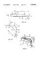
- probe 10designed according to the method of the invention is shown in FIG. 1A.
- probe 10has a bottom edge 12, a top edge 14, a tip 16, and a distal end 18.
- Bottom edge 12is approximately straight while top edge 14 is curved.
- the curvature of top edge 14is fitted to a parabola between tip 16 and an inflection point 19.
- the end of top edge 14 and commencement of tip 16is marked by an end point 15.
- End point 15is collinear with bottom edge 12, as indicated by the extension of bottom edge 12 labelled with Z.
- the computations for determining the appropriate parabolaare set forth below.
- Probe 10has a reference width, W, computed between inflection point 19 and bottom edge 12. Furthermore, the part of probe 10 between inflection point 19 and tip 16 defines a beam section 20 of length L.
- the length, L, of beam section 20is around 60 mil.
- Lcan range from 30 to 200 mil or beyond, however, a significantly longer or shorter beam section 20 is undesirable for mechanical reasons.
- the reference width, Wcustomarily ranges between 2 and 10 mil or more in order to produce sufficient deflection as discussed below.
- FIG. 1Bshows the details of tip 16.
- Tip 16has an outer edge 21 extending from end point 15 to a point of contact 13.
- An inner edge 23 of tip 16continues from point of contact 13 to bottom edge 12 of beam section 20.
- inner edgeis straight opposite outer edge 21, and has a knee section 25 for joining smoothly to bottom edge 12.
- a reference breadth Mis defined between end point 15 and inner edge 23, as shown. The distance between point of contact 13 and end point 15 defines a tip length T.
- FIG. 2illustrates probe 10 being mounted in a groove 26 of a support structure 24.
- Structure 24is preferably made of a ceramic material.
- groove 26can be easily machined by a laser, e.g., excimer laser.
- Probe 10has a width, b, preferably equal to about 1 mil. That is because typical pads which need to be contacted by point of contact 13 during testing can have a width of as little as 2.0 mil and a pitch of 2.9 mil.
- the width and depth of groove 26are sufficient to accommodate probe 10. In this embodiment the width of groove 26 is 1.1 mil and its depth is 5 mils. Distal end 18 of probe 10 is fixed inside groove 26.
- Support structurehas a slot 28 for receiving tab 22.
- slot 28is rectangular to accommodate tab 22 of same shape.
- Distal end 18 of probe 10 and tip 16can be better aligned by using tab 22.
- a vacuumis applied through slot 28.
- Tab 22is drawn into slot 28 and causes probe 10 to align itself properly inside groove 26. Additional disposing of x-y-z, ⁇ arms for grabbing tip 16 or distal end 18 and moving them into proper position can also be used. A persons skilled in the art is conversant with these techniques and devices.
- Probe 10is bonded to the walls of groove 26 once properly aligned. This is preferably done by soldering or adhesive bonding of a part of distal end 18 to the wall of groove 26. Specific bonding techniques are well-known in the art. In bonded probe 10 beam section 20 can move freely up and down over a range of at least 3 mil. Also, beam section 20 is secured against side-buckling by the walls of groove 26. Meanwhile, distal end 18 is rigidly attached inside groove 26.
- bis the thickness of the probe
- ⁇is the stress
- Xis the distance of beam section 20
- Fis the test force experienced by tip 16.
- the shape of tip 16is also predetermined by fitting its outer edge 21 to a second parabola calculated in the same manner as the parabola for beam section 20.
- the breadth m(x) of the second parabolais computed as follows: ##EQU4## wherein b is the thickness of the probe, ⁇ is the stress, and x varies from 0 to length T of tip 16.
- F 1is the component of test force F normal to tip 16, as illustrated in FIG. 1B.
- FIG. 3shows how probe 10 reacts to an overdrive urging tip 16 against a pad 30 on a test wafer 32.
- probe 10hovers over pad 30 as indicated by the solid outline.
- An overdriveis applied in the direction of arrow A. This is done by either lowering structure 24 or raising wafer 32 according to well-known testing methods.
- the F 1 component of force F(see FIG. 1B) will cause tip 16 to perform a scrubbing movement, as shown in FIG. 4. This movement will occur in the direction of arrow B and is typically very short, 1 mil or less. Nonetheless, scrubbing is very important in the testing process because it removes an oxide layer 34 and any impurities (not shown) accumulated on top of pad 32. A good electrical contact between tip 16 and pad 32 is thus guaranteed.
- Probe 10 having a parabolic curvature of beam section 20is very advantageous. It resists fatigue because of uniform stress distribution inside the beam section. Unlike conventional probes, it is not prone to breaking at the point of attachment, and is simple in construction. Furthermore, the life of the probe is extended as well.
- FIG. 5shows another embodiment of a probe 40 according to the invention.
- Probe 40has a top edge 42, a bottom edge 44, a beam portion 46, and a tip 48 with an outer edge 49.
- Tip 48is shown resting on top of pad 30 of wafer 32.
- the essential difference between the preferred embodimentis that the parabolic curvature of top edge 42 and the parabolic curvature of outer edge 49 is approximated by straight sections 50. This is done for practical reasons, since shaping top edge 42 and outer edge 49 to conform to the first and second parabolas can be very difficult.
- each parabolais approximated by two straight sections 50 in the embodiment shown in FIG. 5, any number of such sections can be used. In fact, an entire parabola, e.g., the parabola of top edge 42, can be approximated by one straight section. Otherwise, the operation and advantages of this embodiment are the same as those disclosed for the preferred implementation above.
- FIG. 6illustrates a number of probes 60 with parabolic curvature of top edges 62.
- Probes 60are mounted for carrying out an actual test.
- a test circuit 64 with pads 66is positioned directly under tips 68.
- a support structure 70 with a long slot 72 for receiving tabs 74preserves surmounts probes 60 to provide lateral stability and guide the probes.
- Distal ends 76 of probes 60are attached to a probe card 80 by solder junctions 78.
- FIG. 7depicts the positions of tips 68 more clearly. In particular, grooves 82 are visible in this perspective view. Although all tips 68 appear in the same plane in FIG. 7, in practice deviations of 1.5 mil between the plane of the die and the plane of the probe tips are common. This lack of planarity is compensated by a longer overdrive. In particular, to ensure a 3 mil deflection of beam sections 62 the overdrive should be at least 4.5 mil. The first 1.5 mil will compensate for planarity deviations and the remaining 3 mil will produce the desired deflection and scrubbing.
- tips 68are first sanded after mounting (as described above) to achieve a planarity of 0.3 mil. Because of the parabolic shape of top edges 62 probes 60 will maintain this planarity over a very large number of cycles.
- FIG. 8shows a specially treated tip 90 of a probe 92 according to the invention.
- a coating 94encapsulates tip 90. The addition of such coating can take place after sanding of tip 90. Electroplating, sputtering, or any other suitable processes can be used to deposit coating 94. Conventional, wear-resistant coatings are preferred, e.g., the MP35N cobalt alloy or rhodium.
- the presented probe design method and probes produced according to itshould be viewed as exemplary of the invention. Many modifications to the method are possible. For example, the curvature of the parabolas can be approximated by other geometrical forms than straight sections. Additionally, the support structure with grooves can be left out in cases where side-buckling does not occur. This happens when the thickness of the probe b is sufficiently large to render the probe laterally rigid. In this instance the probe can be mounted on a support structure without grooves according to traditional techniques.
Landscapes
- Measuring Leads Or Probes (AREA)
- Testing Or Measuring Of Semiconductors Or The Like (AREA)
Abstract
Description
Claims (6)
Priority Applications (1)
| Application Number | Priority Date | Filing Date | Title |
|---|---|---|---|
| US08/440,521US5720098A (en) | 1995-05-12 | 1995-05-12 | Method for making a probe preserving a uniform stress distribution under deflection |
Applications Claiming Priority (1)
| Application Number | Priority Date | Filing Date | Title |
|---|---|---|---|
| US08/440,521US5720098A (en) | 1995-05-12 | 1995-05-12 | Method for making a probe preserving a uniform stress distribution under deflection |
Publications (1)
| Publication Number | Publication Date |
|---|---|
| US5720098Atrue US5720098A (en) | 1998-02-24 |
Family
ID=23749086
Family Applications (1)
| Application Number | Title | Priority Date | Filing Date |
|---|---|---|---|
| US08/440,521Expired - Fee RelatedUS5720098A (en) | 1995-05-12 | 1995-05-12 | Method for making a probe preserving a uniform stress distribution under deflection |
Country Status (1)
| Country | Link |
|---|---|
| US (1) | US5720098A (en) |
Cited By (63)
| Publication number | Priority date | Publication date | Assignee | Title |
|---|---|---|---|---|
| US6208155B1 (en)* | 1998-01-27 | 2001-03-27 | Cerprobe Corporation | Probe tip and method for making electrical contact with a solder ball contact of an integrated circuit device |
| US6211687B1 (en)* | 1996-12-02 | 2001-04-03 | Tan Yin Leong | Connector contact fingers for testing integrated circuit packages |
| US6256882B1 (en)* | 1998-07-14 | 2001-07-10 | Cascade Microtech, Inc. | Membrane probing system |
| US6294922B1 (en)* | 1996-02-13 | 2001-09-25 | Nihon Denshizairyo Kabushiki Kaisha | Probe for testing a semiconductor integrated circuit |
| US6352454B1 (en)* | 1999-10-20 | 2002-03-05 | Xerox Corporation | Wear-resistant spring contacts |
| US20020067181A1 (en)* | 1993-11-16 | 2002-06-06 | Formfactor, Inc. | Probe card assembly and kit, and methods of making same |
| US20020075019A1 (en)* | 2000-12-04 | 2002-06-20 | Leonard Hayden | Wafer probe |
| US6426637B1 (en) | 1999-12-21 | 2002-07-30 | Cerprobe Corporation | Alignment guide and signal transmission apparatus and method for spring contact probe needles |
| US6437584B1 (en) | 1996-08-08 | 2002-08-20 | Cascade Microtech, Inc. | Membrane probing system with local contact scrub |
| US6489795B1 (en) | 2001-05-18 | 2002-12-03 | Anthony G. Klele | High-frequency test probe assembly for microcircuits and associated methods |
| US20030006787A1 (en)* | 2000-06-28 | 2003-01-09 | Toshio Kazama | Conductive contact |
| US6511900B2 (en) | 1999-08-24 | 2003-01-28 | Micron Technology, Inc. | Boron incorporated diffusion barrier material |
| US6518181B2 (en) | 1999-04-06 | 2003-02-11 | Micron Technology, Inc. | Conductive material for integrated circuit fabrication |
| US20030090278A1 (en)* | 2001-08-21 | 2003-05-15 | Kenneth Smith | Membrane probing system |
| US6578264B1 (en) | 1999-06-04 | 2003-06-17 | Cascade Microtech, Inc. | Method for constructing a membrane probe using a depression |
| US20030132767A1 (en)* | 2000-02-25 | 2003-07-17 | Tervo Paul A. | Membrane probing system |
| US6615485B2 (en)* | 1993-11-16 | 2003-09-09 | Formfactor, Inc. | Probe card assembly and kit, and methods of making same |
| US6701612B2 (en) | 1993-11-16 | 2004-03-09 | Formfactor, Inc. | Method and apparatus for shaping spring elements |
| US6788080B1 (en) | 2003-05-15 | 2004-09-07 | Seymour Lenz | Test probe assembly for circuits, circuit element arrays, and associated methods |
| US6812692B2 (en)* | 2001-08-30 | 2004-11-02 | Murata Manufacturing Co., Ltd | Inspection terminal for inspecting electronic chip component, and inspection method and inspection apparatus using the same |
| US6836962B2 (en)* | 1993-11-16 | 2005-01-04 | Formfactor, Inc. | Method and apparatus for shaping spring elements |
| US20050035777A1 (en)* | 1997-05-28 | 2005-02-17 | Randy Schwindt | Probe holder for testing of a test device |
| US20050083074A1 (en)* | 2003-10-20 | 2005-04-21 | Industrial Technology Research Institute | Integrated probe module for LCD panel light inspection |
| US6937037B2 (en) | 1995-11-09 | 2005-08-30 | Formfactor, Et Al. | Probe card assembly for contacting a device with raised contact elements |
| US20060006889A1 (en)* | 2004-07-07 | 2006-01-12 | Kenneth Smith | Probe head having a membrane suspended probe |
| US20060006887A1 (en)* | 2004-07-09 | 2006-01-12 | January Kister | Cantilever probe with dual plane fixture and probe apparatus therewith |
| US7161363B2 (en) | 2002-05-23 | 2007-01-09 | Cascade Microtech, Inc. | Probe for testing a device under test |
| US20070007974A1 (en)* | 2005-07-05 | 2007-01-11 | Jinn-Tong Chiu | Method for reducing integral stress of a vertical probe with specific structure |
| US20070152686A1 (en)* | 2004-05-21 | 2007-07-05 | January Kister | Knee probe having increased scrub motion |
| US7271603B2 (en) | 2003-05-23 | 2007-09-18 | Cascade Microtech, Inc. | Shielded probe for testing a device under test |
| USD553030S1 (en)* | 2005-10-21 | 2007-10-16 | Toptronic Limited | Instrument for detecting which electrical plug is connected to a particular circuit breaker |
| US7285969B2 (en) | 2002-11-13 | 2007-10-23 | Cascade Microtech, Inc. | Probe for combined signals |
| US20070285085A1 (en)* | 2006-06-12 | 2007-12-13 | Cascade Microtech, Inc. | Differential signal probing system |
| US20070285111A1 (en)* | 2006-06-12 | 2007-12-13 | Cascade Microtech, Inc. | Test structure and probe for differential signals |
| US20080001612A1 (en)* | 2004-05-21 | 2008-01-03 | January Kister | Probes with self-cleaning blunt skates for contacting conductive pads |
| US20080068035A1 (en)* | 2006-09-14 | 2008-03-20 | Microprobe, Inc. | Knee probe having reduced thickness section for control of scrub motion |
| US20080088327A1 (en)* | 2006-10-11 | 2008-04-17 | January Kister | Probe cards employing probes having retaining portions for potting in a potting region |
| US7420381B2 (en) | 2004-09-13 | 2008-09-02 | Cascade Microtech, Inc. | Double sided probing structures |
| US7427868B2 (en) | 2003-12-24 | 2008-09-23 | Cascade Microtech, Inc. | Active wafer probe |
| US7443186B2 (en) | 2006-06-12 | 2008-10-28 | Cascade Microtech, Inc. | On-wafer test structures for differential signals |
| US7449899B2 (en) | 2005-06-08 | 2008-11-11 | Cascade Microtech, Inc. | Probe for high frequency signals |
| US20090102495A1 (en)* | 2007-10-19 | 2009-04-23 | January Kister | Vertical guided probe array providing sideways scrub motion |
| US7535247B2 (en) | 2005-01-31 | 2009-05-19 | Cascade Microtech, Inc. | Interface for testing semiconductors |
| US20090201041A1 (en)* | 2007-04-10 | 2009-08-13 | Microprobe, Inc. | Vertical Probe Array Arranged to Provide Space Transformation |
| US20090224787A1 (en)* | 2008-03-05 | 2009-09-10 | Promos Technologies Inc. | Probing apparatus for measuring electrical properties of integrated circuit devices on semiconductor wafer |
| US7609077B2 (en) | 2006-06-09 | 2009-10-27 | Cascade Microtech, Inc. | Differential signal probe with integral balun |
| US7619419B2 (en) | 2005-06-13 | 2009-11-17 | Cascade Microtech, Inc. | Wideband active-passive differential signal probe |
| US20090293274A1 (en)* | 2008-05-29 | 2009-12-03 | January Kister | Probe bonding method having improved control of bonding material |
| US7656172B2 (en) | 2005-01-31 | 2010-02-02 | Cascade Microtech, Inc. | System for testing semiconductors |
| US20100085069A1 (en)* | 2008-10-06 | 2010-04-08 | Smith Kenneth R | Impedance optimized interface for membrane probe application |
| US20100109691A1 (en)* | 2005-12-07 | 2010-05-06 | Microprobe, Inc. | Low Profile Probe Having Improved Mechanical Scrub and Reduced Contact Inductance |
| US7723999B2 (en) | 2006-06-12 | 2010-05-25 | Cascade Microtech, Inc. | Calibration structures for differential signal probing |
| US20100127725A1 (en)* | 2008-11-21 | 2010-05-27 | Smith Kenneth R | Replaceable coupon for a probing apparatus |
| US20100176832A1 (en)* | 2007-10-19 | 2010-07-15 | Microprobe, Inc. | Vertical Guided Layered Probe |
| US20100182031A1 (en)* | 2004-05-21 | 2010-07-22 | Microprobe, Inc. | Layered Probes With Core |
| US20100220752A1 (en)* | 2009-03-02 | 2010-09-02 | Polaronyx, Inc. | 810 nm Ultra-Short Pulsed Fiber Laser |
| US20110006796A1 (en)* | 2006-10-11 | 2011-01-13 | Microprobe, Inc. | Probe retention arrangement |
| US7876114B2 (en) | 2007-08-08 | 2011-01-25 | Cascade Microtech, Inc. | Differential waveguide probe |
| US20110062978A1 (en)* | 2004-05-21 | 2011-03-17 | Microprobe, Inc. | Multiple contact probes |
| USRE43503E1 (en) | 2006-06-29 | 2012-07-10 | Microprobe, Inc. | Probe skates for electrical testing of convex pad topologies |
| US8373428B2 (en) | 1993-11-16 | 2013-02-12 | Formfactor, Inc. | Probe card assembly and kit, and methods of making same |
| USRE44407E1 (en) | 2006-03-20 | 2013-08-06 | Formfactor, Inc. | Space transformers employing wire bonds for interconnections with fine pitch contacts |
| US9476911B2 (en) | 2004-05-21 | 2016-10-25 | Microprobe, Inc. | Probes with high current carrying capability and laser machining methods |
Citations (5)
| Publication number | Priority date | Publication date | Assignee | Title |
|---|---|---|---|---|
| US3599093A (en)* | 1969-04-28 | 1971-08-10 | Rca Corp | Apparatus including a wire tipped probe for testing semiconductor wafers |
| US3812311A (en)* | 1972-12-11 | 1974-05-21 | Electronic Memories & Magnetic | Miniature type switch probe for testing integrated circuit assemblies or the like |
| DE3014127A1 (en)* | 1979-05-09 | 1980-11-27 | Elektromat Veb | Probe for testing semiconductor chips - is made from cold workable material formed into taper with perpendicular contact tip at narrowest end |
| US4618821A (en)* | 1983-09-19 | 1986-10-21 | Lenz Seymour S | Test probe assembly for microelectronic circuits |
| US5457882A (en)* | 1991-11-12 | 1995-10-17 | International Business Machines Corporation | Method of making conductive molded tip head assembly |
- 1995
- 1995-05-12USUS08/440,521patent/US5720098A/ennot_activeExpired - Fee Related
Patent Citations (5)
| Publication number | Priority date | Publication date | Assignee | Title |
|---|---|---|---|---|
| US3599093A (en)* | 1969-04-28 | 1971-08-10 | Rca Corp | Apparatus including a wire tipped probe for testing semiconductor wafers |
| US3812311A (en)* | 1972-12-11 | 1974-05-21 | Electronic Memories & Magnetic | Miniature type switch probe for testing integrated circuit assemblies or the like |
| DE3014127A1 (en)* | 1979-05-09 | 1980-11-27 | Elektromat Veb | Probe for testing semiconductor chips - is made from cold workable material formed into taper with perpendicular contact tip at narrowest end |
| US4618821A (en)* | 1983-09-19 | 1986-10-21 | Lenz Seymour S | Test probe assembly for microelectronic circuits |
| US5457882A (en)* | 1991-11-12 | 1995-10-17 | International Business Machines Corporation | Method of making conductive molded tip head assembly |
Cited By (169)
| Publication number | Priority date | Publication date | Assignee | Title |
|---|---|---|---|---|
| US8373428B2 (en) | 1993-11-16 | 2013-02-12 | Formfactor, Inc. | Probe card assembly and kit, and methods of making same |
| US6836962B2 (en)* | 1993-11-16 | 2005-01-04 | Formfactor, Inc. | Method and apparatus for shaping spring elements |
| US6701612B2 (en) | 1993-11-16 | 2004-03-09 | Formfactor, Inc. | Method and apparatus for shaping spring elements |
| US20020067181A1 (en)* | 1993-11-16 | 2002-06-06 | Formfactor, Inc. | Probe card assembly and kit, and methods of making same |
| US6615485B2 (en)* | 1993-11-16 | 2003-09-09 | Formfactor, Inc. | Probe card assembly and kit, and methods of making same |
| US7086149B2 (en) | 1993-11-16 | 2006-08-08 | Formfactor, Inc. | Method of making a contact structure with a distinctly formed tip structure |
| US6937037B2 (en) | 1995-11-09 | 2005-08-30 | Formfactor, Et Al. | Probe card assembly for contacting a device with raised contact elements |
| US6294922B1 (en)* | 1996-02-13 | 2001-09-25 | Nihon Denshizairyo Kabushiki Kaisha | Probe for testing a semiconductor integrated circuit |
| US6300783B1 (en)* | 1996-02-13 | 2001-10-09 | Nihon Denshizairyo Kabushiki Kaisha | Probe, manufacture of same, and vertically operative type probe card assembly employing same |
| US6437584B1 (en) | 1996-08-08 | 2002-08-20 | Cascade Microtech, Inc. | Membrane probing system with local contact scrub |
| US20090224783A1 (en)* | 1996-08-08 | 2009-09-10 | Cascade Microtech, Inc. | Membrane probing system with local contact scrub |
| US7893704B2 (en) | 1996-08-08 | 2011-02-22 | Cascade Microtech, Inc. | Membrane probing structure with laterally scrubbing contacts |
| US7109731B2 (en) | 1996-08-08 | 2006-09-19 | Cascade Microtech, Inc. | Membrane probing system with local contact scrub |
| US7541821B2 (en) | 1996-08-08 | 2009-06-02 | Cascade Microtech, Inc. | Membrane probing system with local contact scrub |
| US20020135388A1 (en)* | 1996-08-08 | 2002-09-26 | Gleason K. Reed | Membrane probing system with local contact scrub |
| US6927585B2 (en) | 1996-08-08 | 2005-08-09 | Cascade Microtech, Inc. | Membrane probing system with local contact scrub |
| US20050231223A1 (en)* | 1996-08-08 | 2005-10-20 | Cascade Microtech, Inc. | Membrane probing system with local contact scrub |
| US6211687B1 (en)* | 1996-12-02 | 2001-04-03 | Tan Yin Leong | Connector contact fingers for testing integrated circuit packages |
| US20050035777A1 (en)* | 1997-05-28 | 2005-02-17 | Randy Schwindt | Probe holder for testing of a test device |
| US7504842B2 (en) | 1997-05-28 | 2009-03-17 | Cascade Microtech, Inc. | Probe holder for testing of a test device |
| US6208155B1 (en)* | 1998-01-27 | 2001-03-27 | Cerprobe Corporation | Probe tip and method for making electrical contact with a solder ball contact of an integrated circuit device |
| US20070283555A1 (en)* | 1998-07-14 | 2007-12-13 | Cascade Microtech, Inc. | Membrane probing system |
| US6860009B2 (en) | 1998-07-14 | 2005-03-01 | Cascade Microtech, Inc. | Probe construction using a recess |
| US7400155B2 (en) | 1998-07-14 | 2008-07-15 | Cascade Microtech, Inc. | Membrane probing system |
| US20050136562A1 (en)* | 1998-07-14 | 2005-06-23 | Reed Gleason | Membrane probing system |
| US6256882B1 (en)* | 1998-07-14 | 2001-07-10 | Cascade Microtech, Inc. | Membrane probing system |
| US6708386B2 (en)* | 1998-07-14 | 2004-03-23 | Cascade Microtech, Inc. | Method for probing an electrical device having a layer of oxide thereon |
| US8451017B2 (en)* | 1998-07-14 | 2013-05-28 | Cascade Microtech, Inc. | Membrane probing method using improved contact |
| US7266889B2 (en) | 1998-07-14 | 2007-09-11 | Cascade Microtech, Inc. | Membrane probing system |
| US20040093716A1 (en)* | 1998-07-14 | 2004-05-20 | Reed Gleason | Membrane probing system |
| US7761986B2 (en) | 1998-07-14 | 2010-07-27 | Cascade Microtech, Inc. | Membrane probing method using improved contact |
| US20040154155A1 (en)* | 1998-07-14 | 2004-08-12 | Reed Gleason | Membrane probing system |
| US20100271060A1 (en)* | 1998-07-14 | 2010-10-28 | Cascade Microtech, Inc. | Membrane probing method using improved contact |
| US7681312B2 (en) | 1998-07-14 | 2010-03-23 | Cascade Microtech, Inc. | Membrane probing system |
| US20070245536A1 (en)* | 1998-07-14 | 2007-10-25 | Cascade Microtech,, Inc. | Membrane probing system |
| US6825677B2 (en) | 1998-07-14 | 2004-11-30 | Cascade Microtech, Inc. | Membrane probing system |
| US6518181B2 (en) | 1999-04-06 | 2003-02-11 | Micron Technology, Inc. | Conductive material for integrated circuit fabrication |
| US20040201398A1 (en)* | 1999-04-06 | 2004-10-14 | Hu Yungjun Jeff | Conductive material for integrated circuit fabrication |
| US6781365B2 (en) | 1999-04-06 | 2004-08-24 | Micron Technology, Inc. | Conductive material for integrated circuit fabrication |
| US20050225340A1 (en)* | 1999-04-06 | 2005-10-13 | Hu Yungjun J | Conductive material for integrated circuit fabrication |
| US6765398B2 (en)* | 1999-04-06 | 2004-07-20 | Micron Technology Inc. | Conductive material for integrated circuit fabrication |
| US7046029B2 (en) | 1999-04-06 | 2006-05-16 | Micron Technology, Inc. | Conductive material for integrated circuit fabrication |
| US6870380B2 (en) | 1999-04-06 | 2005-03-22 | Micron Technology Inc | Conductive material for integrated circuit fabrication |
| US20030183949A1 (en)* | 1999-04-06 | 2003-10-02 | Hu Yungjun Jeff | Conductive material for integrated circuit fabrication |
| US6906547B2 (en) | 1999-04-06 | 2005-06-14 | Micron Technology Inc. | Conductive material for integrated circuit fabrication |
| US6699781B2 (en) | 1999-04-06 | 2004-03-02 | Micron Technology Inc. | Conductive material for integrated circuit fabrication |
| US20030183521A1 (en)* | 1999-04-06 | 2003-10-02 | Hu Yungjun Jeff | Conductive material for integrated circuit fabrication |
| US6646456B2 (en)* | 1999-04-06 | 2003-11-11 | Micron Technology Inc. | Conductive material for integrated circuit fabrication |
| US6578264B1 (en) | 1999-06-04 | 2003-06-17 | Cascade Microtech, Inc. | Method for constructing a membrane probe using a depression |
| US7178236B2 (en) | 1999-06-04 | 2007-02-20 | Cascade Microtech, Inc. | Method for constructing a membrane probe using a depression |
| US7533462B2 (en) | 1999-06-04 | 2009-05-19 | Cascade Microtech, Inc. | Method of constructing a membrane probe |
| US20040082156A1 (en)* | 1999-08-24 | 2004-04-29 | Agarwal Vishnu K. | Boron incorporated diffusion barrier material |
| US6630391B2 (en) | 1999-08-24 | 2003-10-07 | Micron Technology, Inc. | Boron incorporated diffusion barrier material |
| US20050266624A1 (en)* | 1999-08-24 | 2005-12-01 | Agarwal Vishnu K | Boron incorporated diffusion barrier material |
| US6635939B2 (en) | 1999-08-24 | 2003-10-21 | Micron Technology, Inc. | Boron incorporated diffusion barrier material |
| US6911381B2 (en) | 1999-08-24 | 2005-06-28 | Micron Technology Inc. | Boron incorporated diffusion barrier material |
| US20040080002A1 (en)* | 1999-08-24 | 2004-04-29 | Agarwal Vishnu K. | Boron incorporated diffusion barrier material |
| US7084504B2 (en) | 1999-08-24 | 2006-08-01 | Micron Technology, Inc. | Boron incorporated diffusion barrier material |
| US6511900B2 (en) | 1999-08-24 | 2003-01-28 | Micron Technology, Inc. | Boron incorporated diffusion barrier material |
| US7271092B2 (en) | 1999-08-24 | 2007-09-18 | Micron Technology, Inc. | Boron incorporated diffusion barrier material |
| US20060261421A1 (en)* | 1999-08-24 | 2006-11-23 | Agarwal Vishnu K | Boron incorporated diffusion barrier material |
| US6352454B1 (en)* | 1999-10-20 | 2002-03-05 | Xerox Corporation | Wear-resistant spring contacts |
| US6426637B1 (en) | 1999-12-21 | 2002-07-30 | Cerprobe Corporation | Alignment guide and signal transmission apparatus and method for spring contact probe needles |
| US7403025B2 (en) | 2000-02-25 | 2008-07-22 | Cascade Microtech, Inc. | Membrane probing system |
| US20050007131A1 (en)* | 2000-02-25 | 2005-01-13 | Cascade Microtech, Inc. | Membrane probing system |
| US6838890B2 (en) | 2000-02-25 | 2005-01-04 | Cascade Microtech, Inc. | Membrane probing system |
| US20050248359A1 (en)* | 2000-02-25 | 2005-11-10 | Cascade Microtech, Inc. | Membrane probing system |
| US20030132767A1 (en)* | 2000-02-25 | 2003-07-17 | Tervo Paul A. | Membrane probing system |
| US7148711B2 (en) | 2000-02-25 | 2006-12-12 | Cascade Microtech, Inc. | Membrane probing system |
| US6930498B2 (en) | 2000-02-25 | 2005-08-16 | Cascade Microtech, Inc. | Membrane probing system |
| US20030006787A1 (en)* | 2000-06-28 | 2003-01-09 | Toshio Kazama | Conductive contact |
| US7456646B2 (en) | 2000-12-04 | 2008-11-25 | Cascade Microtech, Inc. | Wafer probe |
| US7495461B2 (en) | 2000-12-04 | 2009-02-24 | Cascade Microtech, Inc. | Wafer probe |
| US7761983B2 (en) | 2000-12-04 | 2010-07-27 | Cascade Microtech, Inc. | Method of assembling a wafer probe |
| US20020075019A1 (en)* | 2000-12-04 | 2002-06-20 | Leonard Hayden | Wafer probe |
| US7688097B2 (en) | 2000-12-04 | 2010-03-30 | Cascade Microtech, Inc. | Wafer probe |
| US7233160B2 (en) | 2000-12-04 | 2007-06-19 | Cascade Microtech, Inc. | Wafer probe |
| US6489795B1 (en) | 2001-05-18 | 2002-12-03 | Anthony G. Klele | High-frequency test probe assembly for microcircuits and associated methods |
| US20030090278A1 (en)* | 2001-08-21 | 2003-05-15 | Kenneth Smith | Membrane probing system |
| US7355420B2 (en) | 2001-08-21 | 2008-04-08 | Cascade Microtech, Inc. | Membrane probing system |
| US7492175B2 (en) | 2001-08-21 | 2009-02-17 | Cascade Microtech, Inc. | Membrane probing system |
| US6812692B2 (en)* | 2001-08-30 | 2004-11-02 | Murata Manufacturing Co., Ltd | Inspection terminal for inspecting electronic chip component, and inspection method and inspection apparatus using the same |
| US7518387B2 (en) | 2002-05-23 | 2009-04-14 | Cascade Microtech, Inc. | Shielded probe for testing a device under test |
| US7304488B2 (en) | 2002-05-23 | 2007-12-04 | Cascade Microtech, Inc. | Shielded probe for high-frequency testing of a device under test |
| US7161363B2 (en) | 2002-05-23 | 2007-01-09 | Cascade Microtech, Inc. | Probe for testing a device under test |
| US7489149B2 (en) | 2002-05-23 | 2009-02-10 | Cascade Microtech, Inc. | Shielded probe for testing a device under test |
| US7436194B2 (en) | 2002-05-23 | 2008-10-14 | Cascade Microtech, Inc. | Shielded probe with low contact resistance for testing a device under test |
| US7482823B2 (en) | 2002-05-23 | 2009-01-27 | Cascade Microtech, Inc. | Shielded probe for testing a device under test |
| US7453276B2 (en) | 2002-11-13 | 2008-11-18 | Cascade Microtech, Inc. | Probe for combined signals |
| US7285969B2 (en) | 2002-11-13 | 2007-10-23 | Cascade Microtech, Inc. | Probe for combined signals |
| US7417446B2 (en) | 2002-11-13 | 2008-08-26 | Cascade Microtech, Inc. | Probe for combined signals |
| US6788080B1 (en) | 2003-05-15 | 2004-09-07 | Seymour Lenz | Test probe assembly for circuits, circuit element arrays, and associated methods |
| US7498829B2 (en) | 2003-05-23 | 2009-03-03 | Cascade Microtech, Inc. | Shielded probe for testing a device under test |
| US7271603B2 (en) | 2003-05-23 | 2007-09-18 | Cascade Microtech, Inc. | Shielded probe for testing a device under test |
| US7501842B2 (en) | 2003-05-23 | 2009-03-10 | Cascade Microtech, Inc. | Shielded probe for testing a device under test |
| US7898273B2 (en) | 2003-05-23 | 2011-03-01 | Cascade Microtech, Inc. | Probe for testing a device under test |
| US7619429B2 (en)* | 2003-10-20 | 2009-11-17 | Industrial Technology Research Institute | Integrated probe module for LCD panel light inspection |
| US20050083074A1 (en)* | 2003-10-20 | 2005-04-21 | Industrial Technology Research Institute | Integrated probe module for LCD panel light inspection |
| US7427868B2 (en) | 2003-12-24 | 2008-09-23 | Cascade Microtech, Inc. | Active wafer probe |
| US7759953B2 (en) | 2003-12-24 | 2010-07-20 | Cascade Microtech, Inc. | Active wafer probe |
| US20100182030A1 (en)* | 2004-05-21 | 2010-07-22 | Microprobe, Inc. | Knee Probe Having Reduced Thickness Section for Control of Scrub Motion |
| US7759949B2 (en) | 2004-05-21 | 2010-07-20 | Microprobe, Inc. | Probes with self-cleaning blunt skates for contacting conductive pads |
| US20080001612A1 (en)* | 2004-05-21 | 2008-01-03 | January Kister | Probes with self-cleaning blunt skates for contacting conductive pads |
| US8111080B2 (en) | 2004-05-21 | 2012-02-07 | Microprobe, Inc. | Knee probe having reduced thickness section for control of scrub motion |
| US9316670B2 (en) | 2004-05-21 | 2016-04-19 | Formfactor, Inc. | Multiple contact probes |
| US20100182031A1 (en)* | 2004-05-21 | 2010-07-22 | Microprobe, Inc. | Layered Probes With Core |
| US7733101B2 (en) | 2004-05-21 | 2010-06-08 | Microprobe, Inc. | Knee probe having increased scrub motion |
| US20070152686A1 (en)* | 2004-05-21 | 2007-07-05 | January Kister | Knee probe having increased scrub motion |
| US8988091B2 (en) | 2004-05-21 | 2015-03-24 | Microprobe, Inc. | Multiple contact probes |
| US20110062978A1 (en)* | 2004-05-21 | 2011-03-17 | Microprobe, Inc. | Multiple contact probes |
| US9097740B2 (en) | 2004-05-21 | 2015-08-04 | Formfactor, Inc. | Layered probes with core |
| US9476911B2 (en) | 2004-05-21 | 2016-10-25 | Microprobe, Inc. | Probes with high current carrying capability and laser machining methods |
| US20080157795A1 (en)* | 2004-07-07 | 2008-07-03 | Cascade Microtech, Inc. | Probe head having a membrane suspended probe |
| US7368927B2 (en) | 2004-07-07 | 2008-05-06 | Cascade Microtech, Inc. | Probe head having a membrane suspended probe |
| US20060006889A1 (en)* | 2004-07-07 | 2006-01-12 | Kenneth Smith | Probe head having a membrane suspended probe |
| US7514944B2 (en) | 2004-07-07 | 2009-04-07 | Cascade Microtech, Inc. | Probe head having a membrane suspended probe |
| US8203353B2 (en) | 2004-07-09 | 2012-06-19 | Microprobe, Inc. | Probes with offset arm and suspension structure |
| US7091729B2 (en) | 2004-07-09 | 2006-08-15 | Micro Probe | Cantilever probe with dual plane fixture and probe apparatus therewith |
| US20060006887A1 (en)* | 2004-07-09 | 2006-01-12 | January Kister | Cantilever probe with dual plane fixture and probe apparatus therewith |
| US20100289512A1 (en)* | 2004-07-09 | 2010-11-18 | Microprobe, Inc. | Probes with offset arm and suspension structure |
| US8013623B2 (en) | 2004-09-13 | 2011-09-06 | Cascade Microtech, Inc. | Double sided probing structures |
| US7420381B2 (en) | 2004-09-13 | 2008-09-02 | Cascade Microtech, Inc. | Double sided probing structures |
| US7535247B2 (en) | 2005-01-31 | 2009-05-19 | Cascade Microtech, Inc. | Interface for testing semiconductors |
| US7656172B2 (en) | 2005-01-31 | 2010-02-02 | Cascade Microtech, Inc. | System for testing semiconductors |
| US7940069B2 (en) | 2005-01-31 | 2011-05-10 | Cascade Microtech, Inc. | System for testing semiconductors |
| US7898281B2 (en) | 2005-01-31 | 2011-03-01 | Cascade Mircotech, Inc. | Interface for testing semiconductors |
| US7449899B2 (en) | 2005-06-08 | 2008-11-11 | Cascade Microtech, Inc. | Probe for high frequency signals |
| US7619419B2 (en) | 2005-06-13 | 2009-11-17 | Cascade Microtech, Inc. | Wideband active-passive differential signal probe |
| US20070007974A1 (en)* | 2005-07-05 | 2007-01-11 | Jinn-Tong Chiu | Method for reducing integral stress of a vertical probe with specific structure |
| USD553030S1 (en)* | 2005-10-21 | 2007-10-16 | Toptronic Limited | Instrument for detecting which electrical plug is connected to a particular circuit breaker |
| US8415963B2 (en) | 2005-12-07 | 2013-04-09 | Microprobe, Inc. | Low profile probe having improved mechanical scrub and reduced contact inductance |
| US7944224B2 (en) | 2005-12-07 | 2011-05-17 | Microprobe, Inc. | Low profile probe having improved mechanical scrub and reduced contact inductance |
| US20100109691A1 (en)* | 2005-12-07 | 2010-05-06 | Microprobe, Inc. | Low Profile Probe Having Improved Mechanical Scrub and Reduced Contact Inductance |
| USRE44407E1 (en) | 2006-03-20 | 2013-08-06 | Formfactor, Inc. | Space transformers employing wire bonds for interconnections with fine pitch contacts |
| US7609077B2 (en) | 2006-06-09 | 2009-10-27 | Cascade Microtech, Inc. | Differential signal probe with integral balun |
| US7764072B2 (en) | 2006-06-12 | 2010-07-27 | Cascade Microtech, Inc. | Differential signal probing system |
| US7723999B2 (en) | 2006-06-12 | 2010-05-25 | Cascade Microtech, Inc. | Calibration structures for differential signal probing |
| US7443186B2 (en) | 2006-06-12 | 2008-10-28 | Cascade Microtech, Inc. | On-wafer test structures for differential signals |
| US7403028B2 (en) | 2006-06-12 | 2008-07-22 | Cascade Microtech, Inc. | Test structure and probe for differential signals |
| US20070285085A1 (en)* | 2006-06-12 | 2007-12-13 | Cascade Microtech, Inc. | Differential signal probing system |
| US20070285111A1 (en)* | 2006-06-12 | 2007-12-13 | Cascade Microtech, Inc. | Test structure and probe for differential signals |
| US7750652B2 (en) | 2006-06-12 | 2010-07-06 | Cascade Microtech, Inc. | Test structure and probe for differential signals |
| USRE43503E1 (en) | 2006-06-29 | 2012-07-10 | Microprobe, Inc. | Probe skates for electrical testing of convex pad topologies |
| US7659739B2 (en) | 2006-09-14 | 2010-02-09 | Micro Porbe, Inc. | Knee probe having reduced thickness section for control of scrub motion |
| US20080068035A1 (en)* | 2006-09-14 | 2008-03-20 | Microprobe, Inc. | Knee probe having reduced thickness section for control of scrub motion |
| US8907689B2 (en) | 2006-10-11 | 2014-12-09 | Microprobe, Inc. | Probe retention arrangement |
| US7786740B2 (en) | 2006-10-11 | 2010-08-31 | Astria Semiconductor Holdings, Inc. | Probe cards employing probes having retaining portions for potting in a potting region |
| US9310428B2 (en) | 2006-10-11 | 2016-04-12 | Formfactor, Inc. | Probe retention arrangement |
| US20110006796A1 (en)* | 2006-10-11 | 2011-01-13 | Microprobe, Inc. | Probe retention arrangement |
| US20080088327A1 (en)* | 2006-10-11 | 2008-04-17 | January Kister | Probe cards employing probes having retaining portions for potting in a potting region |
| US20090201041A1 (en)* | 2007-04-10 | 2009-08-13 | Microprobe, Inc. | Vertical Probe Array Arranged to Provide Space Transformation |
| US7952377B2 (en) | 2007-04-10 | 2011-05-31 | Microprobe, Inc. | Vertical probe array arranged to provide space transformation |
| US8324923B2 (en) | 2007-04-10 | 2012-12-04 | Microprobe, Inc. | Vertical probe array arranged to provide space transformation |
| US9274143B2 (en) | 2007-04-10 | 2016-03-01 | Formfactor, Inc. | Vertical probe array arranged to provide space transformation |
| US7876114B2 (en) | 2007-08-08 | 2011-01-25 | Cascade Microtech, Inc. | Differential waveguide probe |
| US8723546B2 (en) | 2007-10-19 | 2014-05-13 | Microprobe, Inc. | Vertical guided layered probe |
| US20090102495A1 (en)* | 2007-10-19 | 2009-04-23 | January Kister | Vertical guided probe array providing sideways scrub motion |
| US20100176832A1 (en)* | 2007-10-19 | 2010-07-15 | Microprobe, Inc. | Vertical Guided Layered Probe |
| US7671610B2 (en) | 2007-10-19 | 2010-03-02 | Microprobe, Inc. | Vertical guided probe array providing sideways scrub motion |
| US20090224787A1 (en)* | 2008-03-05 | 2009-09-10 | Promos Technologies Inc. | Probing apparatus for measuring electrical properties of integrated circuit devices on semiconductor wafer |
| US8230593B2 (en) | 2008-05-29 | 2012-07-31 | Microprobe, Inc. | Probe bonding method having improved control of bonding material |
| US20090293274A1 (en)* | 2008-05-29 | 2009-12-03 | January Kister | Probe bonding method having improved control of bonding material |
| US20100085069A1 (en)* | 2008-10-06 | 2010-04-08 | Smith Kenneth R | Impedance optimized interface for membrane probe application |
| US7888957B2 (en) | 2008-10-06 | 2011-02-15 | Cascade Microtech, Inc. | Probing apparatus with impedance optimized interface |
| US8410806B2 (en) | 2008-11-21 | 2013-04-02 | Cascade Microtech, Inc. | Replaceable coupon for a probing apparatus |
| US20100127725A1 (en)* | 2008-11-21 | 2010-05-27 | Smith Kenneth R | Replaceable coupon for a probing apparatus |
| US9429638B2 (en) | 2008-11-21 | 2016-08-30 | Cascade Microtech, Inc. | Method of replacing an existing contact of a wafer probing assembly |
| US10267848B2 (en) | 2008-11-21 | 2019-04-23 | Formfactor Beaverton, Inc. | Method of electrically contacting a bond pad of a device under test with a probe |
| US20100220752A1 (en)* | 2009-03-02 | 2010-09-02 | Polaronyx, Inc. | 810 nm Ultra-Short Pulsed Fiber Laser |
Similar Documents
| Publication | Publication Date | Title |
|---|---|---|
| US5720098A (en) | Method for making a probe preserving a uniform stress distribution under deflection | |
| US5742174A (en) | Membrane for holding a probe tip in proper location | |
| KR100911676B1 (en) | Contactor, its manufacturing method and test method using contactor | |
| US5773987A (en) | Method for probing a semiconductor wafer using a motor controlled scrub process | |
| CN1103052C (en) | Test Cards with Vertical Probes | |
| US5506515A (en) | High-frequency probe tip assembly | |
| US6529021B1 (en) | Self-scrub buckling beam probe | |
| US5489749A (en) | Semiconductor connection components and method with releasable lead support | |
| US6072324A (en) | Method for testing semiconductor packages using oxide penetrating test contacts | |
| US6100708A (en) | Probe card and wafer testing method using the same | |
| US5917240A (en) | Semiconductor device socket | |
| US7548082B2 (en) | Inspection probe | |
| US20100176832A1 (en) | Vertical Guided Layered Probe | |
| JPH07287952A (en) | Trace interconnect for electrical signals | |
| US6759858B2 (en) | Integrated circuit test probe having ridge contact | |
| KR20170128352A (en) | Contact probe for test head | |
| US3826984A (en) | Measuring device for the dynamic measurement of semiconductor parameters and method of making such a device | |
| KR101019554B1 (en) | Probe and its manufacturing method | |
| US5338223A (en) | Hybrid wafer probe | |
| US20050162177A1 (en) | Multi-signal single beam probe | |
| KR100455499B1 (en) | Probe for inspecting semiconductor device and method of manufacturing the same | |
| JP2811295B2 (en) | Vertical probe card | |
| JPH0837212A (en) | Probe head and test using the probe head | |
| US6825558B2 (en) | Carrier module for μ-BGA type device | |
| JP3356680B2 (en) | Lead frame, semiconductor device, and method of manufacturing semiconductor device |
Legal Events
| Date | Code | Title | Description |
|---|---|---|---|
| AS | Assignment | Owner name:PROBE TECHNOLOGY, CALIFORNIA Free format text:ASSIGNMENT OF ASSIGNORS INTEREST;ASSIGNORS:KISTER, JANUARY;LOBACZ, JERZY;REEL/FRAME:007610/0964 Effective date:19950512 | |
| FEPP | Fee payment procedure | Free format text:PAT HLDR NO LONGER CLAIMS SMALL ENT STAT AS SMALL BUSINESS (ORIGINAL EVENT CODE: LSM2); ENTITY STATUS OF PATENT OWNER: LARGE ENTITY | |
| FPAY | Fee payment | Year of fee payment:4 | |
| REMI | Maintenance fee reminder mailed | ||
| FPAY | Fee payment | Year of fee payment:8 | |
| SULP | Surcharge for late payment | Year of fee payment:7 | |
| AS | Assignment | Owner name:K&S INTERCONNECT, INC., DELAWARE Free format text:MERGER;ASSIGNOR:PROBE TECHNOLOGY CORPORATION;REEL/FRAME:017125/0042 Effective date:20010501 | |
| AS | Assignment | Owner name:SV PROBE PTE LTD., SINGAPORE Free format text:ASSIGNMENT OF ASSIGNORS INTEREST;ASSIGNORS:KULICKE AND SOFFA INDUSTRIES, INC.;K&S INTERCONNECT, INC.;REEL/FRAME:017519/0082 Effective date:20060303 | |
| REMI | Maintenance fee reminder mailed | ||
| LAPS | Lapse for failure to pay maintenance fees | ||
| STCH | Information on status: patent discontinuation | Free format text:PATENT EXPIRED DUE TO NONPAYMENT OF MAINTENANCE FEES UNDER 37 CFR 1.362 | |
| FP | Lapsed due to failure to pay maintenance fee | Effective date:20100224 |