US5719449A - Flip-chip integrated circuit with improved testability - Google Patents
Flip-chip integrated circuit with improved testabilityDownload PDFInfo
- Publication number
- US5719449A US5719449AUS08/724,129US72412996AUS5719449AUS 5719449 AUS5719449 AUS 5719449AUS 72412996 AUS72412996 AUS 72412996AUS 5719449 AUS5719449 AUS 5719449A
- Authority
- US
- United States
- Prior art keywords
- pads
- integrated circuit
- metal layer
- substrate
- chip
- Prior art date
- Legal status (The legal status is an assumption and is not a legal conclusion. Google has not performed a legal analysis and makes no representation as to the accuracy of the status listed.)
- Expired - Lifetime
Links
Images


Classifications
- H—ELECTRICITY
- H01—ELECTRIC ELEMENTS
- H01L—SEMICONDUCTOR DEVICES NOT COVERED BY CLASS H10
- H01L24/00—Arrangements for connecting or disconnecting semiconductor or solid-state bodies; Methods or apparatus related thereto
- H01L24/01—Means for bonding being attached to, or being formed on, the surface to be connected, e.g. chip-to-package, die-attach, "first-level" interconnects; Manufacturing methods related thereto
- H01L24/10—Bump connectors ; Manufacturing methods related thereto
- H—ELECTRICITY
- H01—ELECTRIC ELEMENTS
- H01L—SEMICONDUCTOR DEVICES NOT COVERED BY CLASS H10
- H01L22/00—Testing or measuring during manufacture or treatment; Reliability measurements, i.e. testing of parts without further processing to modify the parts as such; Structural arrangements therefor
- H01L22/30—Structural arrangements specially adapted for testing or measuring during manufacture or treatment, or specially adapted for reliability measurements
- H01L22/32—Additional lead-in metallisation on a device or substrate, e.g. additional pads or pad portions, lines in the scribe line, sacrificed conductors
- H—ELECTRICITY
- H01—ELECTRIC ELEMENTS
- H01L—SEMICONDUCTOR DEVICES NOT COVERED BY CLASS H10
- H01L24/00—Arrangements for connecting or disconnecting semiconductor or solid-state bodies; Methods or apparatus related thereto
- H01L24/01—Means for bonding being attached to, or being formed on, the surface to be connected, e.g. chip-to-package, die-attach, "first-level" interconnects; Manufacturing methods related thereto
- H01L24/10—Bump connectors ; Manufacturing methods related thereto
- H01L24/12—Structure, shape, material or disposition of the bump connectors prior to the connecting process
- H01L24/13—Structure, shape, material or disposition of the bump connectors prior to the connecting process of an individual bump connector
- H—ELECTRICITY
- H01—ELECTRIC ELEMENTS
- H01L—SEMICONDUCTOR DEVICES NOT COVERED BY CLASS H10
- H01L2224/00—Indexing scheme for arrangements for connecting or disconnecting semiconductor or solid-state bodies and methods related thereto as covered by H01L24/00
- H01L2224/01—Means for bonding being attached to, or being formed on, the surface to be connected, e.g. chip-to-package, die-attach, "first-level" interconnects; Manufacturing methods related thereto
- H01L2224/02—Bonding areas; Manufacturing methods related thereto
- H01L2224/0212—Auxiliary members for bonding areas, e.g. spacers
- H01L2224/02122—Auxiliary members for bonding areas, e.g. spacers being formed on the semiconductor or solid-state body
- H01L2224/02163—Auxiliary members for bonding areas, e.g. spacers being formed on the semiconductor or solid-state body on the bonding area
- H01L2224/02165—Reinforcing structures
- H01L2224/02166—Collar structures
- H—ELECTRICITY
- H01—ELECTRIC ELEMENTS
- H01L—SEMICONDUCTOR DEVICES NOT COVERED BY CLASS H10
- H01L2224/00—Indexing scheme for arrangements for connecting or disconnecting semiconductor or solid-state bodies and methods related thereto as covered by H01L24/00
- H01L2224/01—Means for bonding being attached to, or being formed on, the surface to be connected, e.g. chip-to-package, die-attach, "first-level" interconnects; Manufacturing methods related thereto
- H01L2224/02—Bonding areas; Manufacturing methods related thereto
- H01L2224/03—Manufacturing methods
- H01L2224/039—Methods of manufacturing bonding areas involving a specific sequence of method steps
- H01L2224/0392—Methods of manufacturing bonding areas involving a specific sequence of method steps specifically adapted to include a probing step
- H—ELECTRICITY
- H01—ELECTRIC ELEMENTS
- H01L—SEMICONDUCTOR DEVICES NOT COVERED BY CLASS H10
- H01L2224/00—Indexing scheme for arrangements for connecting or disconnecting semiconductor or solid-state bodies and methods related thereto as covered by H01L24/00
- H01L2224/01—Means for bonding being attached to, or being formed on, the surface to be connected, e.g. chip-to-package, die-attach, "first-level" interconnects; Manufacturing methods related thereto
- H01L2224/02—Bonding areas; Manufacturing methods related thereto
- H01L2224/04—Structure, shape, material or disposition of the bonding areas prior to the connecting process
- H01L2224/0401—Bonding areas specifically adapted for bump connectors, e.g. under bump metallisation [UBM]
- H—ELECTRICITY
- H01—ELECTRIC ELEMENTS
- H01L—SEMICONDUCTOR DEVICES NOT COVERED BY CLASS H10
- H01L2224/00—Indexing scheme for arrangements for connecting or disconnecting semiconductor or solid-state bodies and methods related thereto as covered by H01L24/00
- H01L2224/01—Means for bonding being attached to, or being formed on, the surface to be connected, e.g. chip-to-package, die-attach, "first-level" interconnects; Manufacturing methods related thereto
- H01L2224/02—Bonding areas; Manufacturing methods related thereto
- H01L2224/04—Structure, shape, material or disposition of the bonding areas prior to the connecting process
- H01L2224/05—Structure, shape, material or disposition of the bonding areas prior to the connecting process of an individual bonding area
- H01L2224/05001—Internal layers
- H01L2224/05099—Material
- H01L2224/051—Material with a principal constituent of the material being a metal or a metalloid, e.g. boron [B], silicon [Si], germanium [Ge], arsenic [As], antimony [Sb], tellurium [Te] and polonium [Po], and alloys thereof
- H01L2224/05117—Material with a principal constituent of the material being a metal or a metalloid, e.g. boron [B], silicon [Si], germanium [Ge], arsenic [As], antimony [Sb], tellurium [Te] and polonium [Po], and alloys thereof the principal constituent melting at a temperature of greater than or equal to 400°C and less than 950°C
- H01L2224/05124—Aluminium [Al] as principal constituent
- H—ELECTRICITY
- H01—ELECTRIC ELEMENTS
- H01L—SEMICONDUCTOR DEVICES NOT COVERED BY CLASS H10
- H01L2224/00—Indexing scheme for arrangements for connecting or disconnecting semiconductor or solid-state bodies and methods related thereto as covered by H01L24/00
- H01L2224/01—Means for bonding being attached to, or being formed on, the surface to be connected, e.g. chip-to-package, die-attach, "first-level" interconnects; Manufacturing methods related thereto
- H01L2224/10—Bump connectors; Manufacturing methods related thereto
- H01L2224/12—Structure, shape, material or disposition of the bump connectors prior to the connecting process
- H01L2224/13—Structure, shape, material or disposition of the bump connectors prior to the connecting process of an individual bump connector
- H01L2224/13001—Core members of the bump connector
- H01L2224/13099—Material
- H—ELECTRICITY
- H01—ELECTRIC ELEMENTS
- H01L—SEMICONDUCTOR DEVICES NOT COVERED BY CLASS H10
- H01L2924/00—Indexing scheme for arrangements or methods for connecting or disconnecting semiconductor or solid-state bodies as covered by H01L24/00
- H01L2924/01—Chemical elements
- H01L2924/01013—Aluminum [Al]
- H—ELECTRICITY
- H01—ELECTRIC ELEMENTS
- H01L—SEMICONDUCTOR DEVICES NOT COVERED BY CLASS H10
- H01L2924/00—Indexing scheme for arrangements or methods for connecting or disconnecting semiconductor or solid-state bodies as covered by H01L24/00
- H01L2924/01—Chemical elements
- H01L2924/01015—Phosphorus [P]
- H—ELECTRICITY
- H01—ELECTRIC ELEMENTS
- H01L—SEMICONDUCTOR DEVICES NOT COVERED BY CLASS H10
- H01L2924/00—Indexing scheme for arrangements or methods for connecting or disconnecting semiconductor or solid-state bodies as covered by H01L24/00
- H01L2924/013—Alloys
- H01L2924/014—Solder alloys
- H—ELECTRICITY
- H01—ELECTRIC ELEMENTS
- H01L—SEMICONDUCTOR DEVICES NOT COVERED BY CLASS H10
- H01L2924/00—Indexing scheme for arrangements or methods for connecting or disconnecting semiconductor or solid-state bodies as covered by H01L24/00
- H01L2924/10—Details of semiconductor or other solid state devices to be connected
- H01L2924/11—Device type
- H01L2924/14—Integrated circuits
- H—ELECTRICITY
- H01—ELECTRIC ELEMENTS
- H01L—SEMICONDUCTOR DEVICES NOT COVERED BY CLASS H10
- H01L2924/00—Indexing scheme for arrangements or methods for connecting or disconnecting semiconductor or solid-state bodies as covered by H01L24/00
- H01L2924/30—Technical effects
- H01L2924/301—Electrical effects
- H01L2924/30105—Capacitance
- H—ELECTRICITY
- H01—ELECTRIC ELEMENTS
- H01L—SEMICONDUCTOR DEVICES NOT COVERED BY CLASS H10
- H01L2924/00—Indexing scheme for arrangements or methods for connecting or disconnecting semiconductor or solid-state bodies as covered by H01L24/00
- H01L2924/30—Technical effects
- H01L2924/301—Electrical effects
- H01L2924/30107—Inductance
Definitions
- the present inventionrelates to testing integrated circuits (ICs) that are adapted for flip-chip mounting.
- Integrated circuitshave increasingly required a higher number of interconnects for connection to external circuitry, including signal inputs and outputs, and power supply connections.
- the higher numberhas usually been in the form of an increased number of wire bonding pads (“bondpads”) around the periphery of an IC chip. This has often been obtained as the size of IC chips increases, providing for an increased peripheral area, and also as the density of bondpads has increased, due to a smaller size per bondpad.
- bondpadswire bonding pads
- solder bumpsproblems arise when testing a chip on which solder bumps have been formed.
- the traditional technique of testingis to use a multiplicity of semi-rigid wire probes that are pressed onto the metal (e.g., aluminum) chip bondpads to make electrical contact thereto. Then, input/output signals and power supply voltages may be supplied to the chip being tested. This is referred to as "wafer probing", since the IC chips are still attached to one another on a wafer, which is thereafter sawed apart to form the individual chips.
- wafer probingsince the IC chips are still attached to one another on a wafer, which is thereafter sawed apart to form the individual chips.
- attempting to apply test probes to solder bumps formed on the bondpadsmay be difficult, since the relatively soft solder could in some instances cause the probes to stick to the solder bumps.
- the integrated circuitcomprises two sets of pads formed in the same metal layer, with a first set being used for wafer probing, and a second set for solder bumps.
- the wafer probe padsare placed along each chip edge.
- a second set of pads, the solder bump padsare arranged in rows towards the interior of the chip with respect to the wafer probe pads.
- Metal conductorsconnect each solder bump pad to a corresponding wafer probe pad. Testing of the integrated circuit may be accomplished using the wafer probe pads according to conventional techniques, while mounting of the chip may be accomplished with the solder bump pads using the flip-chip technology.
- FIG. 1shows typical prior-art input/output circuitry and associated signal and power bondpads.
- FIG. 2shows an illustrative embodiment of the locations of wafer probe pads and solder bump pads on a chip, and representative ones of the interconnections therebetween.
- FIGS. 3 and 4show a cross-section of an integrated circuit that implements the invention.
- an output buffer 100that includes CMOS transistors 101 and 102 has an output node 104 that is connected to an I/O test pad 105, which is then connected to an I/O solder bump pad 113 by conductor 116.
- an input buffer 106that includes CMOS transistors 107 and 108 has an input node 109 connected to the test pad 105, and thence to solder bump pad 113.
- V DDis supplied to the buffers via solder bump pad 114, conductor 117, and test pad 111
- V SSis supplied via solder bump pad 115, conductor 118 and test pad 112.
- the test padsmay be formed in same location as conventional bondpads around the periphery of the IC, as more fully explained below.
- the solder bump padsmay then be formed in the interior of the IC if desired.
- a semiconductor substrate 201being p-type in the illustrative case, has formed therein doped (n+) contact regions 202 and 203.
- the contact regionsconnect by conductors (not shown for clarity) to the drain 204, or gate 226, or source 205 of a transistor, which may be an input device or an output device as appropriate, as indicated in FIG. 1.
- Contactis made to the regions 202 and 203 by means of first metal (e.g., aluminum) layer 213 through window openings in the dielectric (e.g., boro-phosphosilicate glass) layer designated as 210, 211 and 212.
- first metale.g., aluminum
- dielectrice.g., boro-phosphosilicate glass
- This first metal layeris in turn contacted by a second metal layer 217 through a via opening 218 located in the dielectric (e.g., boro-phospho tetraethylorthosilicate) layer designated as 215 and 216.
- This second metal layerhas formed thereon a dielectric (e.g., silicon nitride) cap layer designated as 219, 220 and 221. Openings as shown in the cap layer allow access to the metal layer 217, providing for a test pad 222, and also for a solder bump pad 224 that may have formed thereon a solder bump 225.
- the test padmay be used in testing the IC by means of wafer probe 223, whereas the solder bump pad 224 and solder bump 225 may be used for flip-chip mounting of the IC, according to techniques known in the art.
- the test pad, solder bump pad, and the conductor that forms the connection therebetweenare formed in the same metal layer.
- the conductor that forms the connectionmay be located in a different metal layer than the metal layer in which the pads are formed, and connected thereto through vias according to techniques known in the art.
- a two-level metal caseis shown illustratively in FIG. 2, the inventive technique may be used with IC's having additional metal levels. For example, in one commercial CMOS process implemented in 0.35 micron technology, four metal levels are used, with the test pad and solder bump pad being formed in the top (e.g. fourth) metal level.
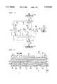
- solder padsare arranged in rows around the periphery of the IC, with five rows shown in the illustrative case.
- Illustrative solder padsare labeled as 301, 302, 303, 304, and 305, with one illustrative pad per row.
- These solder padsallow for a solder bump (not shown) to be applied thereto, so that the IC may be flip-chip mounted to a mounting substrate according to techniques known in the art.
- the present inventionprovides for test pads connected to the solder pads.
- test padsare typically located along the edges of the IC in locations comparable to the conventional wire bonding pads of prior-art ICs.
- the illustrative test pads 306-310are located along the lower edge of the IC (as viewed), and are electrically connected to the corresponding solder pads 301-305, respectively, by means of conductors not shown for clarity. It can be seen that the test pads then provide for the application of test probes to the IC in a conventional manner, so that the IC can be tested prior to mounting.
- solder pad 401is connected to the test pad 406 by means of conductor 411.
- solder pad 402is connected to the test pad 407 by means of conductor 408, and so forth for the other pads shown.
- the test padsmay be staggered along the edge of the IC chip in order to improve linear density.
- the solder pads and test padsare formed in the same conductor (e.g., metal) level.
- the metal conductors that connect the solder pads and the test padsmay be formed in this same conductor level, if desired.
Landscapes
- Engineering & Computer Science (AREA)
- Computer Hardware Design (AREA)
- Microelectronics & Electronic Packaging (AREA)
- Power Engineering (AREA)
- Manufacturing & Machinery (AREA)
- Testing Or Measuring Of Semiconductors Or The Like (AREA)
Abstract
Description
Claims (23)
Priority Applications (1)
| Application Number | Priority Date | Filing Date | Title |
|---|---|---|---|
| US08/724,129US5719449A (en) | 1996-09-30 | 1996-09-30 | Flip-chip integrated circuit with improved testability |
Applications Claiming Priority (1)
| Application Number | Priority Date | Filing Date | Title |
|---|---|---|---|
| US08/724,129US5719449A (en) | 1996-09-30 | 1996-09-30 | Flip-chip integrated circuit with improved testability |
Publications (1)
| Publication Number | Publication Date |
|---|---|
| US5719449Atrue US5719449A (en) | 1998-02-17 |
Family
ID=24909141
Family Applications (1)
| Application Number | Title | Priority Date | Filing Date |
|---|---|---|---|
| US08/724,129Expired - LifetimeUS5719449A (en) | 1996-09-30 | 1996-09-30 | Flip-chip integrated circuit with improved testability |
Country Status (1)
| Country | Link |
|---|---|
| US (1) | US5719449A (en) |
Cited By (55)
| Publication number | Priority date | Publication date | Assignee | Title |
|---|---|---|---|---|
| US5861662A (en)* | 1997-02-24 | 1999-01-19 | General Instrument Corporation | Anti-tamper bond wire shield for an integrated circuit |
| US5962926A (en)* | 1997-09-30 | 1999-10-05 | Motorola, Inc. | Semiconductor device having multiple overlapping rows of bond pads with conductive interconnects and method of pad placement |
| US6008532A (en)* | 1997-10-23 | 1999-12-28 | Lsi Logic Corporation | Integrated circuit package having bond fingers with alternate bonding areas |
| WO2000011718A1 (en)* | 1998-08-22 | 2000-03-02 | Mci Computer Gmbh | Flip-chip type electronic component |
| WO2000039848A3 (en)* | 1998-12-31 | 2000-11-23 | Formfactor Inc | Test method and assembly including a test die for testing a semiconductor product die |
| US6159826A (en)* | 1997-12-29 | 2000-12-12 | Hyundai Electronics Industries Co., Ltd. | Semiconductor wafer and fabrication method of a semiconductor chip |
| US6225702B1 (en)* | 1997-08-29 | 2001-05-01 | Mitsubishi Denki Kabushiki Kaisha | Ball grid array to prevent shorting between a power supply and ground terminal |
| US6303948B1 (en)* | 1996-02-29 | 2001-10-16 | Kabushiki Kaisha Toshiba | Pad layout and lead layout in semiconductor device |
| US6323559B1 (en)* | 1998-06-23 | 2001-11-27 | Lsi Logic Corporation | Hexagonal arrangements of bump pads in flip-chip integrated circuits |
| US6359342B1 (en) | 2000-12-05 | 2002-03-19 | Siliconware Precision Industries Co., Ltd. | Flip-chip bumping structure with dedicated test pads on semiconductor chip and method of fabricating the same |
| US6400170B1 (en)* | 1998-08-26 | 2002-06-04 | Yazaki Corporation | High current examining structure for a circuit protective element |
| US6429029B1 (en) | 1997-01-15 | 2002-08-06 | Formfactor, Inc. | Concurrent design and subsequent partitioning of product and test die |
| US6437431B1 (en)* | 2001-08-07 | 2002-08-20 | Lsi Logic Corporation | Die power distribution system |
| US6445001B2 (en)* | 1996-06-12 | 2002-09-03 | Kabushiki Kaisha Toshiba | Semiconductor device with flip-chip structure and method of manufacturing the same |
| US6448171B1 (en) | 2000-05-05 | 2002-09-10 | Aptos Corporation | Microelectronic fabrication having formed therein terminal electrode structure providing enhanced passivation and enhanced bondability |
| US20020164838A1 (en)* | 2001-05-02 | 2002-11-07 | Moon Ow Chee | Flexible ball grid array chip scale packages and methods of fabrication |
| US6495925B1 (en)* | 1998-11-17 | 2002-12-17 | Infineon Technologies A.G. | Semiconductor chip and a lead frame |
| US6511901B1 (en) | 1999-11-05 | 2003-01-28 | Atmel Corporation | Metal redistribution layer having solderable pads and wire bondable pads |
| US6551844B1 (en) | 1997-01-15 | 2003-04-22 | Formfactor, Inc. | Test assembly including a test die for testing a semiconductor product die |
| US20030089978A1 (en)* | 1999-02-26 | 2003-05-15 | Hitachi, Ltd. | Memory-module and a method of manufacturing the same |
| US20030134450A1 (en)* | 2002-01-09 | 2003-07-17 | Lee Teck Kheng | Elimination of RDL using tape base flip chip on flex for die stacking |
| US20030164551A1 (en)* | 2002-03-04 | 2003-09-04 | Lee Teck Kheng | Method and apparatus for flip-chip packaging providing testing capability |
| US20030164540A1 (en)* | 2002-03-04 | 2003-09-04 | Lee Teck Kheng | Semiconductor die packages with recessed interconnecting structures and methods for assembling the same |
| US20030166312A1 (en)* | 2002-03-04 | 2003-09-04 | Lee Teck Kheng | Methods for assembly and packaging of flip chip configured dice with interposer |
| US20030164548A1 (en)* | 2002-03-04 | 2003-09-04 | Lee Teck Kheng | Flip chip packaging using recessed interposer terminals |
| US20030164543A1 (en)* | 2002-03-04 | 2003-09-04 | Teck Kheng Lee | Interposer configured to reduce the profiles of semiconductor device assemblies and packages including the same and methods |
| US6680544B2 (en)* | 2001-06-13 | 2004-01-20 | Via Technologies, Inc. | Flip-chip bump arrangement for decreasing impedance |
| US20040026782A1 (en)* | 2002-08-09 | 2004-02-12 | Noritaka Anzai | Semiconductor device |
| US20040056367A1 (en)* | 1999-12-30 | 2004-03-25 | Jassowski Michael A. | Semiconductor device inlcluding optimized driver layout for integrated circuit with staggered bond pads |
| US6727597B2 (en)* | 1997-12-12 | 2004-04-27 | Intel Corporation | Integrated circuit device having C4 and wire bond connections |
| US6756251B2 (en) | 2001-08-21 | 2004-06-29 | Micron Technology, Inc. | Method of manufacturing microelectronic devices, including methods of underfilling microelectronic components through an underfill aperture |
| US6762505B2 (en)* | 2001-11-29 | 2004-07-13 | Sun Microsystems | 150 degree bump placement layout for an integrated circuit power grid |
| US20040159957A1 (en)* | 2002-03-04 | 2004-08-19 | Lee Teck Kheng | Interposer substrate and wafer scale interposer substrate member for use with flip-chip configured semiconductor dice |
| US20040198033A1 (en)* | 2002-08-20 | 2004-10-07 | Lee Teck Kheng | Double bumping of flexible substrate for first and second level interconnects |
| US20040203206A1 (en)* | 2002-05-01 | 2004-10-14 | Marvell International Ltd. | Flip chip with novel power and ground arrangement |
| US20040232446A1 (en)* | 1999-01-22 | 2004-11-25 | Renesas Technology Corporation | Semiconductor integrated circuit device and manufacture thereof |
| US20050269718A1 (en)* | 1999-12-30 | 2005-12-08 | Jassowski Michael A | Optimized driver layout for integrated circuits with staggered bond pads |
| US20060049511A1 (en)* | 2004-08-31 | 2006-03-09 | Andre Schaefer | Integrated semiconductor circuit and method for producing an integrated semiconductor circuit |
| US20060097386A1 (en)* | 2002-07-29 | 2006-05-11 | Werner Ertle | Semiconductor wafer with electrically connected contact and test areas |
| US20070045862A1 (en)* | 2005-09-01 | 2007-03-01 | Micron Technology, Inc. | Stacked microelectronic devices and methods for manufacturing microelectronic devices |
| SG130073A1 (en)* | 2005-09-01 | 2007-03-20 | Micron Technology Inc | Stacked microelectronic devices and methods for manufacturing microelectronic devices |
| US20070257352A1 (en)* | 2005-12-29 | 2007-11-08 | Hem Takiar | Test pads on flash memory cards |
| US20080093596A1 (en)* | 2006-10-23 | 2008-04-24 | Ji-Young Shin | Semiconductor Device and Method of Fabricating the Same |
| US20080236882A1 (en)* | 2007-03-30 | 2008-10-02 | Sharp Kabushiki Kaisha | Circuit board and method of manufacturing same |
| US20080308946A1 (en)* | 2007-06-15 | 2008-12-18 | Micron Technology, Inc. | Semiconductor assemblies, stacked semiconductor devices, and methods of manufacturing semiconductor assemblies and stacked semiconductor devices |
| US20090289253A1 (en)* | 2008-05-21 | 2009-11-26 | Stats Chippac, Ltd. | Semiconductor Wafer and Method of Forming Sacrificial Bump Pad for Wafer Probing During Wafer Sort Test |
| WO2010049846A3 (en)* | 2008-10-31 | 2010-06-24 | Nxp B.V. | Semiconductor chip, method of manufacturing a semiconductor chip, and method of testing a semiconductor chip |
| US20100327457A1 (en)* | 2008-02-19 | 2010-12-30 | Liquid Design Systems, Inc. | Semiconductor chip and semiconductor device |
| US20120097432A1 (en)* | 2010-10-21 | 2012-04-26 | E Ink Holdings Inc. | Electrode array |
| US8291368B2 (en) | 2010-04-05 | 2012-10-16 | Freescale Semiconductor, Inc. | Method for reducing surface area of pad limited semiconductor die layout |
| US20140290038A1 (en)* | 2013-03-27 | 2014-10-02 | Bae Systems Information And Electronic Systems Integration Inc. | Method for implementing prompt dose mitigating capacitor |
| US20140332811A1 (en)* | 2013-05-12 | 2014-11-13 | Naveen Kumar | Semiconductor device with bond and probe pads |
| US10158043B2 (en) | 2014-05-30 | 2018-12-18 | Mikro Mesa Technolgy Co., Ltd. | Light-emitting diode and method for manufacturing the same |
| US20190237644A1 (en)* | 2018-01-30 | 2019-08-01 | Mikro Mesa Technology Co., Ltd. | Light emitting device with multi-layer isolation structure |
| WO2021035322A1 (en)* | 2019-08-27 | 2021-03-04 | Ceitec - Centro Nacional De Tecnologia Eletrônica Avançada S.A. | Assembly method for chip with exposed test pads and chip with exposed test pads |
Citations (5)
| Publication number | Priority date | Publication date | Assignee | Title |
|---|---|---|---|---|
| US4488267A (en)* | 1982-05-24 | 1984-12-11 | At&T Bell Laboratories | Integrated circuit chips with removable drivers and/or buffers |
| US5206585A (en)* | 1991-12-02 | 1993-04-27 | At&T Bell Laboratories | Methods for testing integrated circuit devices |
| US5212406A (en)* | 1992-01-06 | 1993-05-18 | Eastman Kodak Company | High density packaging of solid state devices |
| US5334857A (en)* | 1992-04-06 | 1994-08-02 | Motorola, Inc. | Semiconductor device with test-only contacts and method for making the same |
| US5594273A (en)* | 1993-07-23 | 1997-01-14 | Motorola Inc. | Apparatus for performing wafer-level testing of integrated circuits where test pads lie within integrated circuit die but overly no active circuitry for improved yield |
- 1996
- 1996-09-30USUS08/724,129patent/US5719449A/ennot_activeExpired - Lifetime
Patent Citations (5)
| Publication number | Priority date | Publication date | Assignee | Title |
|---|---|---|---|---|
| US4488267A (en)* | 1982-05-24 | 1984-12-11 | At&T Bell Laboratories | Integrated circuit chips with removable drivers and/or buffers |
| US5206585A (en)* | 1991-12-02 | 1993-04-27 | At&T Bell Laboratories | Methods for testing integrated circuit devices |
| US5212406A (en)* | 1992-01-06 | 1993-05-18 | Eastman Kodak Company | High density packaging of solid state devices |
| US5334857A (en)* | 1992-04-06 | 1994-08-02 | Motorola, Inc. | Semiconductor device with test-only contacts and method for making the same |
| US5594273A (en)* | 1993-07-23 | 1997-01-14 | Motorola Inc. | Apparatus for performing wafer-level testing of integrated circuits where test pads lie within integrated circuit die but overly no active circuitry for improved yield |
Non-Patent Citations (6)
| Title |
|---|
| Joel Darnauer et al., "Fast Pad Redistribution from Periphery-IO to Area-IO", 1994 IEEE Multi-Chip Module Conference MCMC-94, Mar. 15-17, 1994, Santa Cruz, California, pp. 38-43. |
| Joel Darnauer et al., Fast Pad Redistribution from Periphery IO to Area IO , 1994 IEEE Multi Chip Module Conference MCMC 94, Mar. 15 17, 1994, Santa Cruz, California, pp. 38 43.* |
| Ray Long Day et al.i, A Silicon on Silicon Multichip Module Technology with Integrated Bipolar Components in the Substrate , 1994 IEEE Multi Chip Module Conference MCMC 94, Mar. 15 17, 1994, Santa Cruz, California, pp. 64 67.* |
| Ray-Long Day et al.i, "A Silicon-on-Silicon Multichip Module Technology with Integrated Bipolar Components in the Substrate", 1994 IEEE Multi-Chip Module Conference MCMC-94,Mar. 15-17, 1994, Santa Cruz, California, pp. 64-67. |
| T.D. Dudderar et al., AT&T Surface Mount Assembly: A New Technology for the Large Volume Fabrication of Cost Effective Flip Chip MCMs , Proceedings of the 1994 International Conference on Multichip Modules, sponsored by IEEE, Apr. 13 15, 1994, Denver, Colorado, pp. 266 272.* |
| T.D. Dudderar et al.,"AT&TμSurface Mount Assembly: A New Technology for the Large Volume Fabrication of Cost Effective Flip-Chip MCMs", Proceedings of the 1994 International Conference on Multichip Modules, sponsored by IEEE,Apr. 13-15, 1994, Denver, Colorado, pp. 266-272. |
Cited By (127)
| Publication number | Priority date | Publication date | Assignee | Title |
|---|---|---|---|---|
| US6303948B1 (en)* | 1996-02-29 | 2001-10-16 | Kabushiki Kaisha Toshiba | Pad layout and lead layout in semiconductor device |
| US6617622B2 (en) | 1996-02-29 | 2003-09-09 | Kabushiki Kaisha Toshiba | Pad layout and lead layout in semiconductor device having a center circuit |
| US6445001B2 (en)* | 1996-06-12 | 2002-09-03 | Kabushiki Kaisha Toshiba | Semiconductor device with flip-chip structure and method of manufacturing the same |
| US20040004216A1 (en)* | 1997-01-15 | 2004-01-08 | Formfactor, Inc. | Test assembly including a test die for testing a semiconductor product die |
| US6429029B1 (en) | 1997-01-15 | 2002-08-06 | Formfactor, Inc. | Concurrent design and subsequent partitioning of product and test die |
| US6551844B1 (en) | 1997-01-15 | 2003-04-22 | Formfactor, Inc. | Test assembly including a test die for testing a semiconductor product die |
| US7557596B2 (en) | 1997-01-15 | 2009-07-07 | Formfactor, Inc. | Test assembly including a test die for testing a semiconductor product die |
| US6825052B2 (en) | 1997-01-15 | 2004-11-30 | Formfactor, Inc. | Test assembly including a test die for testing a semiconductor product die |
| US5861662A (en)* | 1997-02-24 | 1999-01-19 | General Instrument Corporation | Anti-tamper bond wire shield for an integrated circuit |
| US6225702B1 (en)* | 1997-08-29 | 2001-05-01 | Mitsubishi Denki Kabushiki Kaisha | Ball grid array to prevent shorting between a power supply and ground terminal |
| US5962926A (en)* | 1997-09-30 | 1999-10-05 | Motorola, Inc. | Semiconductor device having multiple overlapping rows of bond pads with conductive interconnects and method of pad placement |
| US6008532A (en)* | 1997-10-23 | 1999-12-28 | Lsi Logic Corporation | Integrated circuit package having bond fingers with alternate bonding areas |
| US6727597B2 (en)* | 1997-12-12 | 2004-04-27 | Intel Corporation | Integrated circuit device having C4 and wire bond connections |
| US6531709B1 (en) | 1997-12-29 | 2003-03-11 | Hyundai Electronics Industries Co., Ltd. | Semiconductor wafer and fabrication method of a semiconductor chip |
| US6159826A (en)* | 1997-12-29 | 2000-12-12 | Hyundai Electronics Industries Co., Ltd. | Semiconductor wafer and fabrication method of a semiconductor chip |
| US6323559B1 (en)* | 1998-06-23 | 2001-11-27 | Lsi Logic Corporation | Hexagonal arrangements of bump pads in flip-chip integrated circuits |
| WO2000011718A1 (en)* | 1998-08-22 | 2000-03-02 | Mci Computer Gmbh | Flip-chip type electronic component |
| US6400170B1 (en)* | 1998-08-26 | 2002-06-04 | Yazaki Corporation | High current examining structure for a circuit protective element |
| US6495925B1 (en)* | 1998-11-17 | 2002-12-17 | Infineon Technologies A.G. | Semiconductor chip and a lead frame |
| KR100548103B1 (en)* | 1998-12-31 | 2006-02-02 | 폼팩터, 인크. | Test device including test die for semiconductor product die test and semiconductor product die test method |
| WO2000039848A3 (en)* | 1998-12-31 | 2000-11-23 | Formfactor Inc | Test method and assembly including a test die for testing a semiconductor product die |
| US8629481B2 (en) | 1999-01-22 | 2014-01-14 | Renesas Electronics Corporation | Semiconductor integrated circuit device |
| US20040232446A1 (en)* | 1999-01-22 | 2004-11-25 | Renesas Technology Corporation | Semiconductor integrated circuit device and manufacture thereof |
| US7910922B2 (en) | 1999-01-22 | 2011-03-22 | Renesas Electronics Corporation | Semiconductor integrated circuit device and manufacture thereof |
| US7910960B2 (en) | 1999-01-22 | 2011-03-22 | Renesas Electronics Corporation | Semiconductor integrated circuit device with a fuse circuit |
| US20090230448A1 (en)* | 1999-01-22 | 2009-09-17 | Renesas Technology Corp. | Semiconductor integrated circuit device and manufacture thereof |
| US20110140185A1 (en)* | 1999-01-22 | 2011-06-16 | Renesas Electronics Corporation | Semiconductor integrated circuit device and manufacture thereof |
| US7550763B2 (en) | 1999-01-22 | 2009-06-23 | Renesas Technology Corp. | Semiconductor integrated circuit device and manufacture thereof |
| US20070241330A1 (en)* | 1999-01-22 | 2007-10-18 | Asao Nishimura | Semiconductor integrated circuit device and manufacture thereof |
| US6831294B1 (en)* | 1999-01-22 | 2004-12-14 | Renesas Technology Corp. | Semiconductor integrated circuit device having bump electrodes for signal or power only, and testing pads that are not coupled to bump electrodes |
| US7247879B2 (en) | 1999-01-22 | 2007-07-24 | Renesas Technology Corp. | Semiconductor integrated circuit device having particular testing pad arrangement |
| US7102221B2 (en)* | 1999-02-26 | 2006-09-05 | Hitachi, Ltd. | Memory-Module with an increased density for mounting semiconductor chips |
| US20030089978A1 (en)* | 1999-02-26 | 2003-05-15 | Hitachi, Ltd. | Memory-module and a method of manufacturing the same |
| US6511901B1 (en) | 1999-11-05 | 2003-01-28 | Atmel Corporation | Metal redistribution layer having solderable pads and wire bondable pads |
| US20030119297A1 (en)* | 1999-11-05 | 2003-06-26 | Lam Ken M. | Metal redistribution layer having solderable pads and wire bondable pads |
| US6762117B2 (en)* | 1999-11-05 | 2004-07-13 | Atmel Corporation | Method of fabricating metal redistribution layer having solderable pads and wire bondable pads |
| US6577008B2 (en) | 1999-11-05 | 2003-06-10 | Atmel Corporation | Metal redistribution layer having solderable pads and wire bondable pads |
| US20040056367A1 (en)* | 1999-12-30 | 2004-03-25 | Jassowski Michael A. | Semiconductor device inlcluding optimized driver layout for integrated circuit with staggered bond pads |
| US20050269718A1 (en)* | 1999-12-30 | 2005-12-08 | Jassowski Michael A | Optimized driver layout for integrated circuits with staggered bond pads |
| US6784558B2 (en)* | 1999-12-30 | 2004-08-31 | Intel Corporation | Semiconductor device inlcluding optimized driver layout for integrated circuit with staggered bond pads |
| US6448171B1 (en) | 2000-05-05 | 2002-09-10 | Aptos Corporation | Microelectronic fabrication having formed therein terminal electrode structure providing enhanced passivation and enhanced bondability |
| US6359342B1 (en) | 2000-12-05 | 2002-03-19 | Siliconware Precision Industries Co., Ltd. | Flip-chip bumping structure with dedicated test pads on semiconductor chip and method of fabricating the same |
| US7115986B2 (en) | 2001-05-02 | 2006-10-03 | Micron Technology, Inc. | Flexible ball grid array chip scale packages |
| US20020164838A1 (en)* | 2001-05-02 | 2002-11-07 | Moon Ow Chee | Flexible ball grid array chip scale packages and methods of fabrication |
| US6680544B2 (en)* | 2001-06-13 | 2004-01-20 | Via Technologies, Inc. | Flip-chip bump arrangement for decreasing impedance |
| US6437431B1 (en)* | 2001-08-07 | 2002-08-20 | Lsi Logic Corporation | Die power distribution system |
| US20040224437A1 (en)* | 2001-08-21 | 2004-11-11 | Micron Technology, Inc. | Microelectronic devices including underfill apertures |
| US7087994B2 (en) | 2001-08-21 | 2006-08-08 | Micron Technology, Inc. | Microelectronic devices including underfill apertures |
| US6756251B2 (en) | 2001-08-21 | 2004-06-29 | Micron Technology, Inc. | Method of manufacturing microelectronic devices, including methods of underfilling microelectronic components through an underfill aperture |
| US20060267171A1 (en)* | 2001-08-21 | 2006-11-30 | Micron Technology, Inc. | Semiconductor device modules, semiconductor devices, and microelectronic devices |
| US6762505B2 (en)* | 2001-11-29 | 2004-07-13 | Sun Microsystems | 150 degree bump placement layout for an integrated circuit power grid |
| US8441113B2 (en) | 2002-01-09 | 2013-05-14 | Micron Technology, Inc. | Elimination of RDL using tape base flip chip on flex for die stacking |
| US20080074852A1 (en)* | 2002-01-09 | 2008-03-27 | Micron Technology, Inc. | Elimination of RDL using tape base flip chip on flex for die stacking |
| US20030134450A1 (en)* | 2002-01-09 | 2003-07-17 | Lee Teck Kheng | Elimination of RDL using tape base flip chip on flex for die stacking |
| US7189593B2 (en) | 2002-01-09 | 2007-03-13 | Micron Technology, Inc. | Elimination of RDL using tape base flip chip on flex for die stacking |
| US20040219713A1 (en)* | 2002-01-09 | 2004-11-04 | Micron Technology, Inc. | Elimination of RDL using tape base flip chip on flex for die stacking |
| US7129584B2 (en) | 2002-01-09 | 2006-10-31 | Micron Technology, Inc. | Elimination of RDL using tape base flip chip on flex for die stacking |
| US8125065B2 (en) | 2002-01-09 | 2012-02-28 | Micron Technology, Inc. | Elimination of RDL using tape base flip chip on flex for die stacking |
| US7915718B2 (en) | 2002-03-04 | 2011-03-29 | Micron Technology, Inc. | Apparatus for flip-chip packaging providing testing capability |
| US20040159957A1 (en)* | 2002-03-04 | 2004-08-19 | Lee Teck Kheng | Interposer substrate and wafer scale interposer substrate member for use with flip-chip configured semiconductor dice |
| US20060175690A1 (en)* | 2002-03-04 | 2006-08-10 | Lee Teck K | Interposer configured to reduce the profiles of semiconductor device assemblies, packages including the same, and methods |
| US7534660B2 (en) | 2002-03-04 | 2009-05-19 | Micron Technology, Inc. | Methods for assembly and packaging of flip chip configured dice with interposer |
| US7112520B2 (en) | 2002-03-04 | 2006-09-26 | Micron Technology, Inc. | Semiconductor die packages with recessed interconnecting structures and methods for assembling the same |
| US20030164548A1 (en)* | 2002-03-04 | 2003-09-04 | Lee Teck Kheng | Flip chip packaging using recessed interposer terminals |
| US7122907B2 (en) | 2002-03-04 | 2006-10-17 | Micron Technology, Inc. | Interposer substrate and wafer scale interposer substrate member for use with flip-chip configured semiconductor dice |
| US20060240595A1 (en)* | 2002-03-04 | 2006-10-26 | Lee Teck K | Method and apparatus for flip-chip packaging providing testing capability |
| US20030166312A1 (en)* | 2002-03-04 | 2003-09-04 | Lee Teck Kheng | Methods for assembly and packaging of flip chip configured dice with interposer |
| US20040197955A1 (en)* | 2002-03-04 | 2004-10-07 | Lee Teck Kheng | Methods for assembly and packaging of flip chip configured dice with interposer |
| US7145225B2 (en) | 2002-03-04 | 2006-12-05 | Micron Technology, Inc. | Interposer configured to reduce the profiles of semiconductor device assemblies and packages including the same and methods |
| US20060284312A1 (en)* | 2002-03-04 | 2006-12-21 | Lee Teck K | Flip chip packaging using recessed interposer terminals |
| US7161237B2 (en) | 2002-03-04 | 2007-01-09 | Micron Technology, Inc. | Flip chip packaging using recessed interposer terminals |
| US8269326B2 (en) | 2002-03-04 | 2012-09-18 | Micron Technology, Inc. | Semiconductor device assemblies |
| US7569473B2 (en) | 2002-03-04 | 2009-08-04 | Micron Technology, Inc. | Methods of forming semiconductor assemblies |
| US20110204499A1 (en)* | 2002-03-04 | 2011-08-25 | Micron Technology, Inc. | Semiconductor device assemblies |
| US7230330B2 (en) | 2002-03-04 | 2007-06-12 | Micron Technology, Inc. | Semiconductor die packages with recessed interconnecting structures |
| US20030164540A1 (en)* | 2002-03-04 | 2003-09-04 | Lee Teck Kheng | Semiconductor die packages with recessed interconnecting structures and methods for assembling the same |
| US7087460B2 (en) | 2002-03-04 | 2006-08-08 | Micron Technology, Inc. | Methods for assembly and packaging of flip chip configured dice with interposer |
| US7902648B2 (en) | 2002-03-04 | 2011-03-08 | Micron Technology, Inc. | Interposer configured to reduce the profiles of semiconductor device assemblies, packages including the same, and methods |
| US20070231964A1 (en)* | 2002-03-04 | 2007-10-04 | Micron Technology, Inc. | Methods of forming semiconductor assemblies |
| US20030164543A1 (en)* | 2002-03-04 | 2003-09-04 | Teck Kheng Lee | Interposer configured to reduce the profiles of semiconductor device assemblies and packages including the same and methods |
| US7531906B2 (en) | 2002-03-04 | 2009-05-12 | Micron Technology, Inc. | Flip chip packaging using recessed interposer terminals |
| US20030164551A1 (en)* | 2002-03-04 | 2003-09-04 | Lee Teck Kheng | Method and apparatus for flip-chip packaging providing testing capability |
| US7348215B2 (en) | 2002-03-04 | 2008-03-25 | Micron Technology, Inc. | Methods for assembly and packaging of flip chip configured dice with interposer |
| US6975035B2 (en) | 2002-03-04 | 2005-12-13 | Micron Technology, Inc. | Method and apparatus for dielectric filling of flip chip on interposer assembly |
| US6890794B2 (en)* | 2002-05-01 | 2005-05-10 | Marvell Semiconductor Israel Ltd. | Flip chip with novel power and ground arrangement |
| US6861762B1 (en)* | 2002-05-01 | 2005-03-01 | Marvell Semiconductor Israel Ltd. | Flip chip with novel power and ground arrangement |
| US20040203206A1 (en)* | 2002-05-01 | 2004-10-14 | Marvell International Ltd. | Flip chip with novel power and ground arrangement |
| US8044394B2 (en)* | 2002-07-29 | 2011-10-25 | Infineon Technologies Ag | Semiconductor wafer with electrically connected contact and test areas |
| US8753901B2 (en) | 2002-07-29 | 2014-06-17 | Infineon Technologies Ag | Semiconductor wafer with electrically connected contact and test areas |
| US20060097386A1 (en)* | 2002-07-29 | 2006-05-11 | Werner Ertle | Semiconductor wafer with electrically connected contact and test areas |
| US6982494B2 (en)* | 2002-08-09 | 2006-01-03 | Oki Electric Industry Co., Ltd. | Semiconductor device with signal line having decreased characteristic impedance |
| US7538417B2 (en) | 2002-08-09 | 2009-05-26 | Oki Semiconductor Co., Ltd. | Semiconductor device with signal line having decreased characteristic impedance |
| US7239028B2 (en) | 2002-08-09 | 2007-07-03 | Oki Electric Industry Co., Ltd. | Semiconductor device with signal line having decreased characteristic impedance |
| US20070187824A1 (en)* | 2002-08-09 | 2007-08-16 | Noritaka Anzai | Semiconductor device with signal line having decreased characteristic impedance |
| US20060022354A1 (en)* | 2002-08-09 | 2006-02-02 | Noritaka Anzai | Semiconductor device |
| US20040026782A1 (en)* | 2002-08-09 | 2004-02-12 | Noritaka Anzai | Semiconductor device |
| US20040198033A1 (en)* | 2002-08-20 | 2004-10-07 | Lee Teck Kheng | Double bumping of flexible substrate for first and second level interconnects |
| US7320933B2 (en) | 2002-08-20 | 2008-01-22 | Micron Technology, Inc. | Double bumping of flexible substrate for first and second level interconnects |
| US20060049511A1 (en)* | 2004-08-31 | 2006-03-09 | Andre Schaefer | Integrated semiconductor circuit and method for producing an integrated semiconductor circuit |
| DE102004041961B3 (en)* | 2004-08-31 | 2006-03-30 | Infineon Technologies Ag | Integrated semiconductor circuit with integrated capacitance between Kontaktanscluss and substrate and method for their preparation |
| US7749808B2 (en) | 2005-09-01 | 2010-07-06 | Micron Technology, Inc. | Stacked microelectronic devices and methods for manufacturing microelectronic devices |
| SG130073A1 (en)* | 2005-09-01 | 2007-03-20 | Micron Technology Inc | Stacked microelectronic devices and methods for manufacturing microelectronic devices |
| US20070045862A1 (en)* | 2005-09-01 | 2007-03-01 | Micron Technology, Inc. | Stacked microelectronic devices and methods for manufacturing microelectronic devices |
| US20090011541A1 (en)* | 2005-09-01 | 2009-01-08 | Micron Technology, Inc. | Stacked microelectronic devices and methods for manufacturing microelectronic devices |
| US7485969B2 (en) | 2005-09-01 | 2009-02-03 | Micron Technology, Inc. | Stacked microelectronic devices and methods for manufacturing microelectronic devices |
| US7495255B2 (en)* | 2005-12-29 | 2009-02-24 | Sandisk Corporation | Test pads on flash memory cards |
| US20070257352A1 (en)* | 2005-12-29 | 2007-11-08 | Hem Takiar | Test pads on flash memory cards |
| US20080093596A1 (en)* | 2006-10-23 | 2008-04-24 | Ji-Young Shin | Semiconductor Device and Method of Fabricating the Same |
| US7911804B2 (en)* | 2007-03-30 | 2011-03-22 | Sharp Kabushiki Kaisha | Circuit board and method of manufacturing same |
| US20080236882A1 (en)* | 2007-03-30 | 2008-10-02 | Sharp Kabushiki Kaisha | Circuit board and method of manufacturing same |
| US8994163B2 (en) | 2007-06-15 | 2015-03-31 | Micron Technology, Inc. | Semiconductor assemblies, stacked semiconductor devices, and methods of manufacturing semiconductor assemblies and stacked semiconductor devices |
| US9209166B2 (en) | 2007-06-15 | 2015-12-08 | Micron Technology, Inc. | Semiconductor assemblies, stacked semiconductor devices, and methods of manufacturing semiconductor assemblies and stacked semiconductor devices |
| US20080308946A1 (en)* | 2007-06-15 | 2008-12-18 | Micron Technology, Inc. | Semiconductor assemblies, stacked semiconductor devices, and methods of manufacturing semiconductor assemblies and stacked semiconductor devices |
| US8367471B2 (en) | 2007-06-15 | 2013-02-05 | Micron Technology, Inc. | Semiconductor assemblies, stacked semiconductor devices, and methods of manufacturing semiconductor assemblies and stacked semiconductor devices |
| US20100327457A1 (en)* | 2008-02-19 | 2010-12-30 | Liquid Design Systems, Inc. | Semiconductor chip and semiconductor device |
| US8987014B2 (en)* | 2008-05-21 | 2015-03-24 | Stats Chippac, Ltd. | Semiconductor wafer and method of forming sacrificial bump pad for wafer probing during wafer sort test |
| US20090289253A1 (en)* | 2008-05-21 | 2009-11-26 | Stats Chippac, Ltd. | Semiconductor Wafer and Method of Forming Sacrificial Bump Pad for Wafer Probing During Wafer Sort Test |
| WO2010049846A3 (en)* | 2008-10-31 | 2010-06-24 | Nxp B.V. | Semiconductor chip, method of manufacturing a semiconductor chip, and method of testing a semiconductor chip |
| US8291368B2 (en) | 2010-04-05 | 2012-10-16 | Freescale Semiconductor, Inc. | Method for reducing surface area of pad limited semiconductor die layout |
| US20120097432A1 (en)* | 2010-10-21 | 2012-04-26 | E Ink Holdings Inc. | Electrode array |
| US20140290038A1 (en)* | 2013-03-27 | 2014-10-02 | Bae Systems Information And Electronic Systems Integration Inc. | Method for implementing prompt dose mitigating capacitor |
| US9027226B2 (en)* | 2013-03-27 | 2015-05-12 | Bae Systems Information And Electronic Systems Integration Inc. | Method for implementing prompt dose mitigating capacitor |
| US20140332811A1 (en)* | 2013-05-12 | 2014-11-13 | Naveen Kumar | Semiconductor device with bond and probe pads |
| US10158043B2 (en) | 2014-05-30 | 2018-12-18 | Mikro Mesa Technolgy Co., Ltd. | Light-emitting diode and method for manufacturing the same |
| US20190237644A1 (en)* | 2018-01-30 | 2019-08-01 | Mikro Mesa Technology Co., Ltd. | Light emitting device with multi-layer isolation structure |
| CN110097829A (en)* | 2018-01-30 | 2019-08-06 | 美科米尚技术有限公司 | Display device |
| WO2021035322A1 (en)* | 2019-08-27 | 2021-03-04 | Ceitec - Centro Nacional De Tecnologia Eletrônica Avançada S.A. | Assembly method for chip with exposed test pads and chip with exposed test pads |
Similar Documents
| Publication | Publication Date | Title |
|---|---|---|
| US5719449A (en) | Flip-chip integrated circuit with improved testability | |
| US6278181B1 (en) | Stacked multi-chip modules using C4 interconnect technology having improved thermal management | |
| KR101203220B1 (en) | Method and apparatus for providing structural support for interconnect pad while allowing signal conductance | |
| US6833290B2 (en) | Structure and method of forming a multiple leadframe semiconductor device | |
| JP3772066B2 (en) | Semiconductor device | |
| JP3287346B2 (en) | Semiconductor device | |
| US6617692B2 (en) | Apparatus for implementing selected functionality on an integrated circuit device | |
| US6136620A (en) | Method of manufacture for an integrated circuit having a BIST circuit and bond pads incorporated therein | |
| US7687900B2 (en) | Semiconductor integrated circuit device and fabrication method for the same | |
| US6249136B1 (en) | Bottom side C4 bumps for integrated circuits | |
| JPH09139471A (en) | Auxiliary pad for on-circuit-array probing | |
| US3517278A (en) | Flip chip structure | |
| US5117280A (en) | Plastic package semiconductor device with thermal stress resistant structure | |
| US6020746A (en) | Method and apparatus for probing an integrated circuit through the back side of an integrated circuit die | |
| JPH01155637A (en) | Multichip module | |
| US6500699B1 (en) | Test fixture for future integration | |
| JP3395747B2 (en) | Manufacturing method of semiconductor integrated circuit | |
| JPH08181307A (en) | Field-effect power-element integrated circuit | |
| JPS62183134A (en) | Semiconductor device | |
| JPS6273651A (en) | Semiconductor integrated circuit module | |
| JPH1082834A (en) | Semiconductor integrated circuit | |
| JP2001035993A (en) | Multi-chip module and manufacture thereof | |
| JPS6298633A (en) | semiconductor equipment | |
| KR100196222B1 (en) | Manufacturing method of semiconductor chip | |
| JPS61180470A (en) | Semiconductor integrated circuit device |
Legal Events
| Date | Code | Title | Description |
|---|---|---|---|
| AS | Assignment | Owner name:LUCENT TECHNOLOGIES INC., NEW JERSEY Free format text:ASSIGNMENT OF ASSIGNORS INTEREST;ASSIGNOR:STRAUSS, MARK STEVEN;REEL/FRAME:008252/0076 Effective date:19960930 | |
| FEPP | Fee payment procedure | Free format text:PAYOR NUMBER ASSIGNED (ORIGINAL EVENT CODE: ASPN); ENTITY STATUS OF PATENT OWNER: LARGE ENTITY | |
| STCF | Information on status: patent grant | Free format text:PATENTED CASE | |
| FPAY | Fee payment | Year of fee payment:4 | |
| FPAY | Fee payment | Year of fee payment:8 | |
| FPAY | Fee payment | Year of fee payment:12 | |
| AS | Assignment | Owner name:DEUTSCHE BANK AG NEW YORK BRANCH, AS COLLATERAL AG Free format text:PATENT SECURITY AGREEMENT;ASSIGNORS:LSI CORPORATION;AGERE SYSTEMS LLC;REEL/FRAME:032856/0031 Effective date:20140506 | |
| AS | Assignment | Owner name:AVAGO TECHNOLOGIES GENERAL IP (SINGAPORE) PTE. LTD Free format text:ASSIGNMENT OF ASSIGNORS INTEREST;ASSIGNOR:AGERE SYSTEMS LLC;REEL/FRAME:035059/0001 Effective date:20140804 Owner name:AGERE SYSTEMS LLC, PENNSYLVANIA Free format text:MERGER;ASSIGNOR:AGERE SYSTEMS INC.;REEL/FRAME:035058/0895 Effective date:20120724 Owner name:AGERE SYSTEMS INC., PENNSYLVANIA Free format text:MERGER;ASSIGNOR:AGERE SYSTEMS GUARDIAN CORP.;REEL/FRAME:035058/0884 Effective date:20020822 Owner name:AGERE SYSTEMS GUARDIAN CORP., PENNSYLVANIA Free format text:ASSIGNMENT OF ASSIGNORS INTEREST;ASSIGNOR:LUCENT TECHNOLOGIES INC.;REEL/FRAME:035058/0646 Effective date:20010130 | |
| AS | Assignment | Owner name:LSI CORPORATION, CALIFORNIA Free format text:TERMINATION AND RELEASE OF SECURITY INTEREST IN PATENT RIGHTS (RELEASES RF 032856-0031);ASSIGNOR:DEUTSCHE BANK AG NEW YORK BRANCH, AS COLLATERAL AGENT;REEL/FRAME:037684/0039 Effective date:20160201 Owner name:AGERE SYSTEMS LLC, PENNSYLVANIA Free format text:TERMINATION AND RELEASE OF SECURITY INTEREST IN PATENT RIGHTS (RELEASES RF 032856-0031);ASSIGNOR:DEUTSCHE BANK AG NEW YORK BRANCH, AS COLLATERAL AGENT;REEL/FRAME:037684/0039 Effective date:20160201 | |
| AS | Assignment | Owner name:BANK OF AMERICA, N.A., AS COLLATERAL AGENT, NORTH CAROLINA Free format text:PATENT SECURITY AGREEMENT;ASSIGNOR:AVAGO TECHNOLOGIES GENERAL IP (SINGAPORE) PTE. LTD.;REEL/FRAME:037808/0001 Effective date:20160201 Owner name:BANK OF AMERICA, N.A., AS COLLATERAL AGENT, NORTH Free format text:PATENT SECURITY AGREEMENT;ASSIGNOR:AVAGO TECHNOLOGIES GENERAL IP (SINGAPORE) PTE. LTD.;REEL/FRAME:037808/0001 Effective date:20160201 | |
| AS | Assignment | Owner name:AVAGO TECHNOLOGIES GENERAL IP (SINGAPORE) PTE. LTD., SINGAPORE Free format text:TERMINATION AND RELEASE OF SECURITY INTEREST IN PATENTS;ASSIGNOR:BANK OF AMERICA, N.A., AS COLLATERAL AGENT;REEL/FRAME:041710/0001 Effective date:20170119 Owner name:AVAGO TECHNOLOGIES GENERAL IP (SINGAPORE) PTE. LTD Free format text:TERMINATION AND RELEASE OF SECURITY INTEREST IN PATENTS;ASSIGNOR:BANK OF AMERICA, N.A., AS COLLATERAL AGENT;REEL/FRAME:041710/0001 Effective date:20170119 | |
| AS | Assignment | Owner name:BELL SEMICONDUCTOR, LLC, ILLINOIS Free format text:ASSIGNMENT OF ASSIGNORS INTEREST;ASSIGNORS:AVAGO TECHNOLOGIES GENERAL IP (SINGAPORE) PTE. LTD.;BROADCOM CORPORATION;REEL/FRAME:044886/0766 Effective date:20171208 | |
| AS | Assignment | Owner name:CORTLAND CAPITAL MARKET SERVICES LLC, AS COLLATERA Free format text:SECURITY INTEREST;ASSIGNORS:HILCO PATENT ACQUISITION 56, LLC;BELL SEMICONDUCTOR, LLC;BELL NORTHERN RESEARCH, LLC;REEL/FRAME:045216/0020 Effective date:20180124 | |
| AS | Assignment | Owner name:BELL NORTHERN RESEARCH, LLC, ILLINOIS Free format text:RELEASE BY SECURED PARTY;ASSIGNOR:CORTLAND CAPITAL MARKET SERVICES LLC;REEL/FRAME:059723/0382 Effective date:20220401 Owner name:BELL SEMICONDUCTOR, LLC, ILLINOIS Free format text:RELEASE BY SECURED PARTY;ASSIGNOR:CORTLAND CAPITAL MARKET SERVICES LLC;REEL/FRAME:059723/0382 Effective date:20220401 Owner name:HILCO PATENT ACQUISITION 56, LLC, ILLINOIS Free format text:RELEASE BY SECURED PARTY;ASSIGNOR:CORTLAND CAPITAL MARKET SERVICES LLC;REEL/FRAME:059723/0382 Effective date:20220401 |