US5719417A - Ferroelectric integrated circuit structure - Google Patents
Ferroelectric integrated circuit structureDownload PDFInfo
- Publication number
- US5719417A US5719417AUS08/758,600US75860096AUS5719417AUS 5719417 AUS5719417 AUS 5719417AUS 75860096 AUS75860096 AUS 75860096AUS 5719417 AUS5719417 AUS 5719417A
- Authority
- US
- United States
- Prior art keywords
- layer
- orientation
- integrated circuit
- plt
- ferroelectric
- Prior art date
- Legal status (The legal status is an assumption and is not a legal conclusion. Google has not performed a legal analysis and makes no representation as to the accuracy of the status listed.)
- Expired - Lifetime
Links
Images


Classifications
- H—ELECTRICITY
- H01—ELECTRIC ELEMENTS
- H01L—SEMICONDUCTOR DEVICES NOT COVERED BY CLASS H10
- H01L21/00—Processes or apparatus adapted for the manufacture or treatment of semiconductor or solid state devices or of parts thereof
- H01L21/02—Manufacture or treatment of semiconductor devices or of parts thereof
- H01L21/02104—Forming layers
- H01L21/02107—Forming insulating materials on a substrate
- H01L21/02109—Forming insulating materials on a substrate characterised by the type of layer, e.g. type of material, porous/non-porous, pre-cursors, mixtures or laminates
- H01L21/02112—Forming insulating materials on a substrate characterised by the type of layer, e.g. type of material, porous/non-porous, pre-cursors, mixtures or laminates characterised by the material of the layer
- H01L21/02172—Forming insulating materials on a substrate characterised by the type of layer, e.g. type of material, porous/non-porous, pre-cursors, mixtures or laminates characterised by the material of the layer the material containing at least one metal element, e.g. metal oxides, metal nitrides, metal oxynitrides or metal carbides
- H01L21/02197—Forming insulating materials on a substrate characterised by the type of layer, e.g. type of material, porous/non-porous, pre-cursors, mixtures or laminates characterised by the material of the layer the material containing at least one metal element, e.g. metal oxides, metal nitrides, metal oxynitrides or metal carbides the material having a perovskite structure, e.g. BaTiO3
- H—ELECTRICITY
- H10—SEMICONDUCTOR DEVICES; ELECTRIC SOLID-STATE DEVICES NOT OTHERWISE PROVIDED FOR
- H10D—INORGANIC ELECTRIC SEMICONDUCTOR DEVICES
- H10D1/00—Resistors, capacitors or inductors
- H10D1/60—Capacitors
- H10D1/68—Capacitors having no potential barriers
- H10D1/682—Capacitors having no potential barriers having dielectrics comprising perovskite structures
- H10D1/684—Capacitors having no potential barriers having dielectrics comprising perovskite structures the dielectrics comprising multiple layers, e.g. comprising buffer layers, seed layers or gradient layers
- H—ELECTRICITY
- H01—ELECTRIC ELEMENTS
- H01L—SEMICONDUCTOR DEVICES NOT COVERED BY CLASS H10
- H01L21/00—Processes or apparatus adapted for the manufacture or treatment of semiconductor or solid state devices or of parts thereof
- H01L21/02—Manufacture or treatment of semiconductor devices or of parts thereof
- H01L21/02104—Forming layers
- H01L21/02107—Forming insulating materials on a substrate
- H01L21/02109—Forming insulating materials on a substrate characterised by the type of layer, e.g. type of material, porous/non-porous, pre-cursors, mixtures or laminates
- H01L21/02112—Forming insulating materials on a substrate characterised by the type of layer, e.g. type of material, porous/non-porous, pre-cursors, mixtures or laminates characterised by the material of the layer
- H01L21/02123—Forming insulating materials on a substrate characterised by the type of layer, e.g. type of material, porous/non-porous, pre-cursors, mixtures or laminates characterised by the material of the layer the material containing silicon
- H01L21/02164—Forming insulating materials on a substrate characterised by the type of layer, e.g. type of material, porous/non-porous, pre-cursors, mixtures or laminates characterised by the material of the layer the material containing silicon the material being a silicon oxide, e.g. SiO2
- H—ELECTRICITY
- H01—ELECTRIC ELEMENTS
- H01L—SEMICONDUCTOR DEVICES NOT COVERED BY CLASS H10
- H01L21/00—Processes or apparatus adapted for the manufacture or treatment of semiconductor or solid state devices or of parts thereof
- H01L21/02—Manufacture or treatment of semiconductor devices or of parts thereof
- H01L21/02104—Forming layers
- H01L21/02107—Forming insulating materials on a substrate
- H01L21/02109—Forming insulating materials on a substrate characterised by the type of layer, e.g. type of material, porous/non-porous, pre-cursors, mixtures or laminates
- H01L21/02112—Forming insulating materials on a substrate characterised by the type of layer, e.g. type of material, porous/non-porous, pre-cursors, mixtures or laminates characterised by the material of the layer
- H01L21/02172—Forming insulating materials on a substrate characterised by the type of layer, e.g. type of material, porous/non-porous, pre-cursors, mixtures or laminates characterised by the material of the layer the material containing at least one metal element, e.g. metal oxides, metal nitrides, metal oxynitrides or metal carbides
- H01L21/02175—Forming insulating materials on a substrate characterised by the type of layer, e.g. type of material, porous/non-porous, pre-cursors, mixtures or laminates characterised by the material of the layer the material containing at least one metal element, e.g. metal oxides, metal nitrides, metal oxynitrides or metal carbides characterised by the metal
- H01L21/02189—Forming insulating materials on a substrate characterised by the type of layer, e.g. type of material, porous/non-porous, pre-cursors, mixtures or laminates characterised by the material of the layer the material containing at least one metal element, e.g. metal oxides, metal nitrides, metal oxynitrides or metal carbides characterised by the metal the material containing zirconium, e.g. ZrO2
- H—ELECTRICITY
- H01—ELECTRIC ELEMENTS
- H01L—SEMICONDUCTOR DEVICES NOT COVERED BY CLASS H10
- H01L21/00—Processes or apparatus adapted for the manufacture or treatment of semiconductor or solid state devices or of parts thereof
- H01L21/02—Manufacture or treatment of semiconductor devices or of parts thereof
- H01L21/02104—Forming layers
- H01L21/02107—Forming insulating materials on a substrate
- H01L21/02109—Forming insulating materials on a substrate characterised by the type of layer, e.g. type of material, porous/non-porous, pre-cursors, mixtures or laminates
- H01L21/022—Forming insulating materials on a substrate characterised by the type of layer, e.g. type of material, porous/non-porous, pre-cursors, mixtures or laminates the layer being a laminate, i.e. composed of sublayers, e.g. stacks of alternating high-k metal oxides
- H—ELECTRICITY
- H01—ELECTRIC ELEMENTS
- H01L—SEMICONDUCTOR DEVICES NOT COVERED BY CLASS H10
- H01L21/00—Processes or apparatus adapted for the manufacture or treatment of semiconductor or solid state devices or of parts thereof
- H01L21/02—Manufacture or treatment of semiconductor devices or of parts thereof
- H01L21/02104—Forming layers
- H01L21/02107—Forming insulating materials on a substrate
- H01L21/02225—Forming insulating materials on a substrate characterised by the process for the formation of the insulating layer
- H01L21/0226—Forming insulating materials on a substrate characterised by the process for the formation of the insulating layer formation by a deposition process
- H01L21/02263—Forming insulating materials on a substrate characterised by the process for the formation of the insulating layer formation by a deposition process deposition from the gas or vapour phase
- H01L21/02266—Forming insulating materials on a substrate characterised by the process for the formation of the insulating layer formation by a deposition process deposition from the gas or vapour phase deposition by physical ablation of a target, e.g. sputtering, reactive sputtering, physical vapour deposition or pulsed laser deposition
- H—ELECTRICITY
- H01—ELECTRIC ELEMENTS
- H01L—SEMICONDUCTOR DEVICES NOT COVERED BY CLASS H10
- H01L21/00—Processes or apparatus adapted for the manufacture or treatment of semiconductor or solid state devices or of parts thereof
- H01L21/02—Manufacture or treatment of semiconductor devices or of parts thereof
- H01L21/02104—Forming layers
- H01L21/02107—Forming insulating materials on a substrate
- H01L21/02225—Forming insulating materials on a substrate characterised by the process for the formation of the insulating layer
- H01L21/0226—Forming insulating materials on a substrate characterised by the process for the formation of the insulating layer formation by a deposition process
- H01L21/02263—Forming insulating materials on a substrate characterised by the process for the formation of the insulating layer formation by a deposition process deposition from the gas or vapour phase
- H01L21/02271—Forming insulating materials on a substrate characterised by the process for the formation of the insulating layer formation by a deposition process deposition from the gas or vapour phase deposition by decomposition or reaction of gaseous or vapour phase compounds, i.e. chemical vapour deposition
Definitions
- This inventionrelates to an integrated circuit structure and method of making that structure, and more particularly to a thin layer structure having ferroelectric properties.
- Ferroelectric materialsare presently finding increased application in devices including non-volatile ferroelectric random access memories (NV-FeRAMs), uncooled infrared (IR) detectors, spatial light modulators, and microelectromechanical systems. Many of these applications require optimized ferroelectric properties. Due to the anisotropic nature of ferroelectric materials, such as Pb(Zr,Ti)O 3 (PZT), orientation control may be used to produce thin films or layers with optimized electrical properties.
- NV-FeRAMsnon-volatile ferroelectric random access memories
- IRinfrared
- PZTPb(Zr,Ti)O 3
- orientation controlmay be used to produce thin films or layers with optimized electrical properties.
- Ferroelectric PZTexists in two forms at ambient temperatures: a tetragonal phase, in which the polar vector is aligned parallel to the 001! direction (or c-axis) and a rhombohedral phase in which the polar axis is aligned along the 111! direction.
- anisotropyexists in a number of electric properties, including dielectric constant, remanent polarization, and pyroelectric coefficient.
- Uncooled IR detectorsrequire a high pyroelectric coefficient (p) and low dielectric constant (.di-elect cons.) for maximum voltage responsivity, which is proportional to p/.di-elect cons..
- the maximum pyroelectric coefficientis found along the c-axis.
- the minimum dielectric constantis also found along the c-axis of the crystal. It is thus highly advantageous to control orientation in a thin film or layer such that the c-axis is perpendicular to the plane of the film for a parallel plate capacitor geometry wherein the electrodes lie above and below the film and within parallel planes.
- a film in which the a-axis is oriented perpendicular to the plane of the film for a parallel plate capacitor geometryresults in low pyroelectric coefficient and high dielectric constant, which minimizes voltage responsivity.
- a 111! oriented tetragonal filmrepresents an intermediate case because the average properties of the film can be expressed by resolving the anisotropy into the rectangular coordinates by simple vector algebra.
- rhombohedral ferroelectric PZTmaximum pyroelectric response can be attained in 111! oriented films.
- NV-FeRAMsrequire high remanent polarization to minimize performance requirements of sense amplifiers which read the stored charge.
- low switching voltagesi.e., low coercive fields
- coercive fielddecreases with increasing Zr content, making high Zr compositions desirable.
- a 111! oriented rhombohedral PZT filmmaximizes the remanent polarization
- a 111! oriented tetragonal PZT filmhas a higher polarization than a 100! oriented tetragonal PZT film. This also occurs because the average properties of the film or layer can be expressed by resolving the anisotropy into the rectangular coordinates by simple vector algebra.
- One method to control orientationis by utilizing substrate materials with a coefficient of thermal expansion (CTE) mismatched to that of the ferroelectric film. If the CTE of the substrate is higher than that of the film, the film will be in a state of compression on cooling through the Curie point, (i.e., the temperature where the crystalline phase transforms from the high temperature cubic (paraelectric) state to the low temperature tetragonal (ferroelectric) state. This situation results in a tetragonal film with a preferred 001!orientation. A substrate leading to this orientation must have a CTE larger than the CTE of PZT. MgO is such a substrate material.
- Sisilicon
- Siis the semiconducting substrate of choice for monolithic integration of ferroelectric material with integrated circuits.
- Siliconhas a CTE that is less than that of PZT, so a PZT film deposited on a silicon substrate goes into tension on cooling through the Curie point, resulting in a highly undesirable 100! orientation.
- CTEcoefficient of thermal expansion
- the present invention to control crystal orientation in ferroelectric thin filmsmay in general have advantages for any substrate, since the bottom electrode is typically isolated from the semiconducting substrate by insulating layers that may have adhesion promoting or diffusion barrier properties.
- Substrates of the greatest technological interestare Si, GaAs, Ge, InP and any other semiconductor materials that would allow monolithic integration of the ferroelectric capacitor with transistors fabricated in the same substrate.
- substratessuch as glass or ceramics, or metals, where the transistors reside in another substrate, and are connected to the ferroelectric capacitors in a hybrid configuration.
- Another method for manipulating thin film orientationincludes using seed layers.
- the orientationis very sensitive to changes in A-site/B-site ratio.
- Changing the Pb/Ti ratio in a thin film of PbTiO 3shifts the lattice orientation from 100! for Pb-rich films to 111! for Ti-rich films.
- M. Shimizu, M. Sugiyama, H. Fujisawa, T. Hamano, T. Shiosaki, and K. Matsushige"Effects of the Utilization of a Buffer Layer on the Growth of Pb(Zr,Ti)O 3 Thin Films by Metalorganic Chemical Vapor Deposition, J. Crystal Growth, Vol.
- the 111! oriented seed layer resulting from a low A/B site ratiois useful for depositing thereon a high Zr content ferroelectric film because the polar axis in the high Zr content ferroelectric film is also along the 111! axis.
- PbTiO 3 crystal orientationis influenced by the A-site/B-site ratio
- PZTis not similarly influenced.
- the Ti-rich filmswhich result in the desired 111! lattice orientation, also have a potential to generate oxygen vacancies, as charge compensation for excess Ti. These oxygen vacancies cause undesirable electrical conduction in the perovskite film. Oxygen vacancies may also interact with domain walls to cause fatigue and imprint.
- a ferroelectric layer of PZT with a predetermined crystal lattice orientationcan be deposited over the seed layer.
- the seed layercan be deposited to a sufficient thickness to utilize its own ferroelectric properties.
- the substrate in the foregoing processmay be any suitable material, for example silicon, gallium arsenide, indium phosphide, or germanium.
- the seed layer crystal lattice orientation of the PLT, or seed layeris controlled by a ratio of lead (Pb) plus lanthanum (La) to titanium (Ti) in an A-site to B-site ratio.
- the seed layeris formed of a combination of materials including lead (Pb), lanthanum (La), titanium (Ti) and oxygen (O). Lead and lanthanum occupy A-sites of the crystal lattice structure.
- orientation of the crystal lattice structureis determined by the ratio of lead plus lanthanum to titanium.
- Orientation of the crystal lattice structure of the ferroelectric PZT layeris determined by the orientation of the crystal lattice structure of the seed layer.
- the ferroelectric PZT layeris lead zirconium titanite having a tetragonal or rhombohedral crystalline lattice structure.
- all of the components of the seed layerincluding lead, lanthanum, titanium and oxygen, are deposited simultaneously by chemical vapor deposition (CVD) using dissimilar precursors.
- CVDchemical vapor deposition
- the vaporization of the precursors for transport into the CVD reactormay be accomplished with a single vaporizer or by the use of multiple vaporizers.
- Another aspectis an integrated circuit structure having an adhesion layer deposited on a substrate.
- a conductive layeris deposited over the adhesion layer.
- a seed layeris deposited over the conductive layer with a controlled crystal lattice orientation.
- a ferroelectric layeris deposited over the seed layer causing a predetermined crystal lattice orientation.
- the seed layeris grown to a thickness sufficient to use its intrinsic ferroelectric properties.
- the seed layeris a combination of materials including lead, lanthanum, titanium, and oxygen.
- Lead and lanthanumoccupy A-sites of the crystal lattice structure.
- Titaniumoccupies B-sites. Orientation of the crystal lattice structure is determined by the ratio of lead and lanthanum to titanium in an A-site/B-site ratio.
- FIG. 1shows a cross-sectional view of a silicon substrate with an adhesion layer
- FIG. 2shows the cross-sectional view of FIG. 1 following deposition of a layer of conductive material
- FIG. 3is a cross-sectional view of the structure of FIG. 2 after a layer of seed or PLT material is deposited over the layer of conductive material;
- FIG. 4shows a cross-section of the structure of FIG. 3 following deposition of a layer of ferroelectric PZT material on the seed layer;
- FIG. 5is a schematic drawing of a multiple vaporizer apparatus arranged for simultaneous metalorganic chemical vapor deposition of dissimilar vaporization characteristics precursor materials
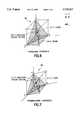
- FIG. 6is a perspective view of a tetragonal crystal lattice orientation of a ferroelectric material
- FIG. 7is a perspective view of a rhombohedral crystal lattice orientation of a ferroelectric material
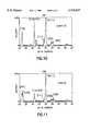
- FIG. 8is an x-ray diffraction (XRD) pattern for a PLT film having an A-site/B-site ratio of 1.03;
- FIG. 9is an x-ray diffraction (XRD) pattern for a PLT film having an A-site/B-site ratio of 0.99;
- FIG. 10is an x-ray diffraction (XRD) pattern for a PZT film having an A/B site ratio of 1.00;
- FIG. 11is an x-ray diffraction (XRD) pattern for a PZT film having an A-site/B-site ratio of 0.87;
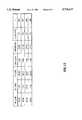
- FIG. 12is a table of illustrative values of parameters for different layers of PLT with various compositions.
- the substrate 25may be a silicon (Si) substrate.
- Other substrate materialsmay also be used as for example GaAs, InP, or Ge.
- the adhesion layeris shown as two separate layers.
- a first layer 31, deposited on top of the substrate 25,is a layer of silicon dioxide (SiO 2 ), which may be native SiO 2 or a deposited layer of SiO 2 , whose thickness may be suitably varied in accordance within the skill of the art.
- the adhesion layer 33is deposited on the substrate for providing material that adheres well to both the silicon substrate 25 and a layer to be deposited on top of the adhesion layer.
- Other non-conductive or conductive materialsmay be used for the adhesion layer 33, for example, Ti, TiO 2 , Zr, Hf, HfO 2 , Ta, Ta 2 O 5 , TiN, TaN, etc.
- the layers 31 and 33may be deposited by well known chemical vapor deposition or physical vapor deposition techniques.
- FIG. 2there is shown the cross-section of the partial device 20 of FIG. 1 upon which a conductive layer 35 is deposited over the top of the layer of zirconium oxide 33 included in the adhesion layer 27.
- the conductive layer 35may be selected from a group of noble metals including, for example, platinum (Pt), rhodium (Rh), and palladium (Pd).
- Ptplatinum
- Rhrhodium
- Pdpalladium
- Non-noble metals and other suitable conductors, such as conductive oxidesmay also be used for the conductive layer 35.
- This conductive layer 35may be deposited to a thickness of approximately 500-3,000 ⁇ by conventional chemical vapor deposition or physical vapor deposition techniques.
- FIG. 3there is shown the cross-section of the device 20 of FIG.
- a seed layer 37that includes lead (Pb), lanthanum (La), titanium (Ti) and oxygen (O) in a material (Pb, La)TiO 3 , generally referred to as PLT.
- the seed layer 37is deposited by a metalorganic chemical vapor deposition (MOCVD) process to a thickness ranging approximately from 100 to 1,500 ⁇ .
- MOCVDmetalorganic chemical vapor deposition
- the A-site/B-site ratio of the PLT materialis controlled precisely during deposition to determine a preferred orientation of the crystalline lattice structure of the seed layer 37.
- the lead and the lanthanumare believed to occupy A-sites in the crystal lattice structure.
- Lanthanumfunctions as a donor dopant La Pb o ! in the lattice because it has a +3 charge and replaces lead which has a +2 charge.
- donor doping of a layer containing Pblowers electrical conductivity in the layer because the donor doping balances Pb deficiency in that layer.
- the Pb deficiencyleads to Pb vacancies V Pb "!.
- the Pb vacanciesIn the absence of acceptor dopants residing in the B-sites A B '!, the Pb vacancies generally are compensated by oxygen vacancies V O oo !. Ionic conduction thus results in such a layer.
- the different layers of the seed layer structurecan be deposited in different chambers or in one chamber.
- PVDphysical vapor deposition
- sputtering or evaporationmay be used for one of the layers, in conjunction with CVD.
- PVDmay be used for all of the layers.
- Different chambersmay be physically separated or may be connected with a vacuum load-lock and the substrates manipulated by a robot (this last configuration is known as a cluster tool).
- a preferred embodimentis for all the layers to be deposited by CVD and in that case multiple chambers may be used, or the different layers may be deposited in a single CVD chamber using multiple vaporizers.
- a PLT seed layerto control the orientation of a PZT film, one technique would be to vaporize Pb and Ti precursors in a vaporizer held at 200° C., to vaporize the La precursor in a vaporizer held at 220° C., and to vaporize the Zr precursor in a vaporizer held at 230° C.
- the PLT seed layerwould be deposited using the first two vaporizers, and Pb/La ratio and the (Pb+La)/Ti ratio of the resulting thin film would be controlled so as to achieve 111! crystal orientation.
- the compositionwould be controlled by manipulating the liquid flow rates to the separate vaporizers and the solution concentrations, as well as the other deposition parameters such as P, gas flow rates, and substrate temperature. Electrical leakage currents in the PLT film would be lower because oxygen anion vacancies would be compensated by the La donor dopant as described above.
- the gaseous La precursor flowwould be diverted to the bypass and the gaseous Zr precursor would be switched to flow to the reactor, enabling deposition of PZT. Fine control of the timing of those switching operations would be needed to achieve the desired composition profile and the optimum electrical and physical properties. Control of the PZT composition would be performed in a manner similar to PLT. Once the PZT film was of sufficient thickness, the gaseous Pb-Ti and Zr precursors would be diverted from the reactor and deposition would be complete. In another embodiment the gaseous La precursor would continue to flow to the reactor, resulting in deposition of PLZT, and the composition of that layer would be controlled as described above for PLT.
- FIG. 4there is shown a cross section of the device 20 of FIG. 3 following deposition of another ferroelectric layer 40 onto the seed layer 37 that includes lead (Pb), zirconium (Zr), titanium (Ti) and oxygen (O) in a material Pb(Zr, Ti)O 3 , generally referred to as PZT.
- the ferroelectric layer 40is deposited by a metalorganic chemical vapor deposition (MOCVD) process to a thickness ranging approximately from 100 ⁇ to 100 ⁇ m depending on the intended device application.
- MOCVDmetalorganic chemical vapor deposition
- FIG. 5there is shown a schematic diagram of a multiple vaporizer apparatus 45 for accomplishing chemical vapor deposition (CVD) of multiple precursor materials that have dissimilar vaporization characteristics.
- CVDchemical vapor deposition
- FIG. 5a schematic diagram of a multiple vaporizer apparatus 45 for accomplishing chemical vapor deposition (CVD) of multiple precursor materials that have dissimilar vaporization characteristics.
- CVDchemical vapor deposition
- FIG. 5Even though some of the precursor materials require vaporization temperature or pressure conditions differing from others to be used in a single layer of material, the apparatus of FIG. 5 can vaporize all of the precursor materials simultaneously for deposition.
- a first vaporizer 50two or more precursors, such as bis-tetramethylheptanedionatolead, Pb(thd) 2 , which is used for depositing lead (Pb) and titanium (Ti) concurrently, are transmitted simultaneously to the first vaporizer.
- the precursorsare transmitted in respective volumes to achieve the desired stoichiometry.
- These precursorshave vaporization characteristics which are sufficiently similar, particularly in their respective temperatures of vaporization, that they are vaporized together in one vaporizer held at a selected temperature.
- a second vaporizer 60is transmitted to a second vaporizer 60. Quantity of the material to be deposited from this precursor is proportioned with the quantities of the materials to be deposited from the first vaporizer 50 to also achieve the desired stoiciometry in the layer of material to be deposited.
- the second vaporizer 60is held at a second selected temperature which is appropriate for vaporizing its precursor.
- a lanthanum precursoris substituted for the zirconium precursor shown in FIG. 5.
- a carrier fluid or fluidsmay be required to transmit the precursors to the vaporizers 50 and 60 and a deposition chamber where the layer of multi-component material is to be deposited all at once on a substrate or on a substrate with one or more layers of material previously deposited thereon.
- CVD reactor 70is shown as an illustrative deposition chamber.
- the multiple vaporizer apparatus 45 of FIG. 5can be used also to deposit two layers of different materials without recharging the supplies of precursor materials.
- the supply lines to the first vaporizer 50may open for flow of two compatible precursors for deposition of a first layer.
- supply lines to the second vaporizer 60may open for flow of one or more precursors that are non-compatible in vaporization with the precursors for the first vaporizer 50. All of the vaporized precursors now flow together into the deposition chamber.
- a second layer of material having a different composition than the first layeris deposited on the first layer.
- the first layeris selected to be a layer of PLT material.
- PLT filmswere deposited by MOCVD using metalorganic precursors dissolved in an organic solvent which were flash vaporized.
- Pb(thd) 2 , La(thd) 3 , and Ti(OiPr) 2 (thd) 2were used as metalorganic precursors.
- the processwas carried out in an oxidizing ambient at reduced pressure at temperatures between 525°-550° C.
- the processcould also be carried out with other metalorganic precursors or alternatively by physical vapor deposition methods, e.g., sputtering or pulsed laser depositon.
- the PLT materialforms a layer of tetragonal crystalline lattice structure with a 111! orientation.
- the PLTis deposited to a thickness in a range between 50 ⁇ and 500 ⁇ .
- the crystalline lattice orientation of the seed layer of PLTaffects both the dielectric constant and the pyroelectric coefficient of the resulting layer.
- the second layeris selected to be a layer of PZT material.
- Pb(thd) 2 , La(thd) 3 , and Ti(OiPr) 2 (thd) 2were used as metalorganic precursors.
- Zr(thd) 4was used with Pb(thd) 2 and Ti(OiPr) 2 (thd) 2 .
- the processwas carried out in an oxidizing ambient at reduced pressure at temperatures between 525°-550° C.
- the processcould also be carried out with other metalorganic precursors or alternatively by physical vapor deposition methods, e.g., sputtering or pulsed laser depositon.
- a carrier gassuch as argon may optionally be employed.
- the first (PLT sources) vaporizerwas held at 200° C.
- the second (PZT sources) vaporizerwas held at a temperature of 230° C.
- the precursorswere transmitted to the vaporizers at flow rates controlled to achieve the desired stoichiometry in the grown film. Such flow rates are very system-dependent.
- Ferroelectric PZT layersmay be deposited by this method to a thicknesses commensurate with the device requirements.
- the layer of PZT materialpreferentially forms either a tetragonal or a rhombohedral crystalline lattice structure with a 111! orientation, depending on the Zr to Ti ratio of the PZT film.
- FIG. 6there is shown a perspective view of a portion of a tetragonal crystalline lattice structure 50.
- the tetragonal crystal latticeprovides the maximum ferroelectric effect when the polar vector (oriented parallel with the c-axis) is oriented perpendicular to parallel plate electrodes.
- a sitesare shown as open circles.
- the B-siteis shown as a solid circle.
- FIG. 7there is a perspective view of a portion of a rhombohedral crystalline lattice structure 60. Again there are six planar faces. Each face is a parallelogram. The axes are not at right angles with one another. For a layer of PZT, the rhombohedral crystalline thin film with a 111! orientation provides maximum ferroelectric effect. Bipoles in such a lattice structure of PZT are oriented in the direction of the heavy arrow. A-sites and B-sites are shown in a similar convention, as in FIG. 6.
- FIGS. 8 through 11depict x-ray diffraction (XRD) patterns for two different compositions of lead (Pb), lanthanum (La), and titanium (Ti) layers and two different compositions of lead (Pb), zirconium (Zr), and titanium (Ti) layers, all of which were deposited on Pt/ZrO 2 /SiO 2 /Si substrates by MOCVD at approximately 525° C.-550° C.
- the substrateis silicon
- the adhesion layeris 500 ⁇ of SiO 2 and 500 ⁇ of ZrO 2 .
- the metal layeris 1000 ⁇ of Pt.
- FIG. 8shows the resulting crystalline lattice orientation for a PLT layer having an A-site/B-site ratio equal to 1.03.
- the diffraction peak that is labeled 100!has a much greater magnitude than the peaks labeled 101! and 111!.
- the crystalline lattice orientation for an A-site/B-site ratio, greater than 1.0is predominantly 100! orientation.
- the resulting crystalline lattice orientation for a PLT layer having an A-site/B-site ratio equal to 0.99is nearly 100% 111! orientation.
- the differention peak labeled 111! by a pointerhas a much grater magnitude than the diffraction peaks labeled 100! and 101! indicating that almost all of the crystal lattice is in the 111! orientation.
- FIG. 9shows the orientation for a crystal lattice except that it is a layer of PZT. There are shown high diffraction peaks for orientations 100! and 110/101! and low peak intensities for the orientations 111!, 002!, and 200!.
- the A-site/B-site ratiois equal to 1.0.
- the A-site/B-site ratiois equal to 0.87 for the examined layer of PZT. All of the diffraction peaks are near the same magnitude.
- the crystalline lattice orientation for a layer of PZT materialdoes not appear to change with variation of its A-site/B-site ratio.
- the fact that the crystal lattice orientation does change in a layer of PLT material with variation of the A-site/B-site ratiois a wholly unexpected relationship.
- the unexpected relationship between the A-site/B-site ratio and crystal lattice orientation for PLTis related to a seed layer in a ferroelectric device. It is clear that the relationship also is useful to control the orientation of a PLT layer, as a ferroelectric layer on its own and for other purposes.
Landscapes
- Engineering & Computer Science (AREA)
- Chemical & Material Sciences (AREA)
- Materials Engineering (AREA)
- Physics & Mathematics (AREA)
- Condensed Matter Physics & Semiconductors (AREA)
- General Physics & Mathematics (AREA)
- Manufacturing & Machinery (AREA)
- Computer Hardware Design (AREA)
- Microelectronics & Electronic Packaging (AREA)
- Power Engineering (AREA)
- Semiconductor Memories (AREA)
Abstract
Description
La.sub.Pb.sup.o !+2 V.sub.O.sup.oo !=2 V.sub.Pb "!+ A.sub.B '!
Claims (9)
Priority Applications (3)
| Application Number | Priority Date | Filing Date | Title |
|---|---|---|---|
| US08/758,600US5719417A (en) | 1996-11-27 | 1996-11-27 | Ferroelectric integrated circuit structure |
| PCT/US1997/021673WO1998024125A1 (en) | 1996-11-27 | 1997-11-24 | Controlled orientation of ferroelectric layers |
| US09/024,246US5998236A (en) | 1996-11-27 | 1998-02-17 | Process for controlled orientation of ferroelectric layers |
Applications Claiming Priority (1)
| Application Number | Priority Date | Filing Date | Title |
|---|---|---|---|
| US08/758,600US5719417A (en) | 1996-11-27 | 1996-11-27 | Ferroelectric integrated circuit structure |
Related Child Applications (1)
| Application Number | Title | Priority Date | Filing Date |
|---|---|---|---|
| US09/024,246DivisionUS5998236A (en) | 1996-11-27 | 1998-02-17 | Process for controlled orientation of ferroelectric layers |
Publications (1)
| Publication Number | Publication Date |
|---|---|
| US5719417Atrue US5719417A (en) | 1998-02-17 |
Family
ID=25052354
Family Applications (2)
| Application Number | Title | Priority Date | Filing Date |
|---|---|---|---|
| US08/758,600Expired - LifetimeUS5719417A (en) | 1996-11-27 | 1996-11-27 | Ferroelectric integrated circuit structure |
| US09/024,246Expired - LifetimeUS5998236A (en) | 1996-11-27 | 1998-02-17 | Process for controlled orientation of ferroelectric layers |
Family Applications After (1)
| Application Number | Title | Priority Date | Filing Date |
|---|---|---|---|
| US09/024,246Expired - LifetimeUS5998236A (en) | 1996-11-27 | 1998-02-17 | Process for controlled orientation of ferroelectric layers |
Country Status (2)
| Country | Link |
|---|---|
| US (2) | US5719417A (en) |
| WO (1) | WO1998024125A1 (en) |
Cited By (80)
| Publication number | Priority date | Publication date | Assignee | Title |
|---|---|---|---|---|
| US5876503A (en)* | 1996-11-27 | 1999-03-02 | Advanced Technology Materials, Inc. | Multiple vaporizer reagent supply system for chemical vapor deposition utilizing dissimilar precursor compositions |
| US5913117A (en)* | 1995-03-20 | 1999-06-15 | Samsung Electronics Co., Ltd. | Method for manufacturing ferroelectric capacitor |
| US5972428A (en)* | 1996-03-05 | 1999-10-26 | Symetrix Corporation | Methods and apparatus for material deposition using primer |
| WO2000017921A1 (en)* | 1998-09-18 | 2000-03-30 | Siemens Aktiengesellschaft | Method for producing self-polarized ferro-electric layers, especially pzt layers, with a rhombohedral crystal structure |
| US6060736A (en)* | 1998-02-03 | 2000-05-09 | Fujitsu Limited | Semiconductor device and method of manufacturing the same |
| US6090443A (en)* | 1997-07-18 | 2000-07-18 | Ramtron International Corporation | Multi-layer approach for optimizing ferroelectric film performance |
| US6111284A (en)* | 1998-08-24 | 2000-08-29 | Murata Manufacturing Co., Ltd. | Ferroelectric thin-film device |
| US6121647A (en)* | 1996-06-26 | 2000-09-19 | Tdk Corporation | Film structure, electronic device, recording medium, and process of preparing ferroelectric thin films |
| US6190728B1 (en)* | 1997-09-29 | 2001-02-20 | Yazaki Corporation | Process for forming thin films of functional ceramics |
| WO2001016395A1 (en)* | 1999-08-31 | 2001-03-08 | Micron Technology, Inc. | Titanium containing dielectric films and methods of forming same |
| US6248394B1 (en) | 1998-08-14 | 2001-06-19 | Agere Systems Guardian Corp. | Process for fabricating device comprising lead zirconate titanate |
| US6284588B1 (en) | 1997-12-30 | 2001-09-04 | Hyundai Electronics Industries Co., Ltd. | Method for fabricating ferroelectric memory devices capable of preventing volatility of elements in ferroelectric films |
| US6284434B1 (en)* | 1997-10-20 | 2001-09-04 | Seiko Epson Corporation | Piezoelectric thin film element fabrication method |
| US6287637B1 (en) | 1997-07-18 | 2001-09-11 | Ramtron International Corporation | Multi-layer approach for optimizing ferroelectric film performance |
| US6297085B1 (en)* | 1997-12-11 | 2001-10-02 | Texas Instruments Incorporated | Method for manufacturing ferroelectric capacitor and method for manufacturing ferroelectric memory |
| US20010054733A1 (en)* | 1999-08-30 | 2001-12-27 | Vishnu Agarwal | Capacitors having a capacitor dielectric layer comprising a metal oxide having multiple different metals bonded with oxygen |
| JP2002076295A (en)* | 2000-05-12 | 2002-03-15 | Agilent Technol Inc | Apparatus with multilayer electrical device |
| US20020072253A1 (en)* | 2000-02-10 | 2002-06-13 | Motorola, Inc. | Method of removing an amorphous oxide from a monocrystalline surface |
| US20020076875A1 (en)* | 2000-06-21 | 2002-06-20 | Kiyotaka Wasa | Structure of piezoelectric element and liquid discharge recording head, and method of manufacture therefor |
| US20020096683A1 (en)* | 2001-01-19 | 2002-07-25 | Motorola, Inc. | Structure and method for fabricating GaN devices utilizing the formation of a compliant substrate |
| EP1229569A2 (en) | 2001-01-31 | 2002-08-07 | Fujitsu Limited | Capacitor semiconductor device comprising the same and method of fabricating thereof |
| WO2002031875A3 (en)* | 2000-10-10 | 2003-01-09 | Asm Inc | Dielectric interface films and methods therefor |
| US20030017265A1 (en)* | 2001-07-13 | 2003-01-23 | Cem Basceri | Chemical vapor deposition methods of forming barium strontium titanate comprising dielectric layers |
| US20030015710A1 (en)* | 2001-07-20 | 2003-01-23 | Motorola, Inc. | Fabrication of a wavelength locker within a semiconductor structure |
| US20030022430A1 (en)* | 2001-07-24 | 2003-01-30 | Motorola, Inc. | Structure and method for fabricating configurable transistor devices utilizing the formation of a compliant substrate for materials used to form the same |
| US20030026310A1 (en)* | 2001-08-06 | 2003-02-06 | Motorola, Inc. | Structure and method for fabrication for a lighting device |
| US20030036224A1 (en)* | 2001-08-15 | 2003-02-20 | Motorola, Inc. | Method for manufacturing a substantially integral monolithic apparatus including a plurality of semiconductor materials |
| US20030038311A1 (en)* | 2001-08-17 | 2003-02-27 | Cem Basceri | Capacitor constructions comprising perovskite-type dielectric materials |
| KR100379941B1 (en)* | 2001-03-06 | 2003-04-11 | 주승기 | Fabrication method of large single-grained ferroelectric thin film and fabrication method of ferroelectric memory device using the same |
| US6566147B2 (en) | 2001-02-02 | 2003-05-20 | Micron Technology, Inc. | Method for controlling deposition of dielectric films |
| US20030113949A1 (en)* | 2001-08-06 | 2003-06-19 | Motorola, Inc. | Structure and method for fabrication for a solid-state lightning device |
| US20030207589A1 (en)* | 2002-05-03 | 2003-11-06 | Thoughtbeam, Inc. | Method for growing a monocrystalline oxide layer and for fabricating a semiconductor device on a monocrystalline substrate |
| US20040012037A1 (en)* | 2002-07-18 | 2004-01-22 | Motorola, Inc. | Hetero-integration of semiconductor materials on silicon |
| US6693298B2 (en) | 2001-07-20 | 2004-02-17 | Motorola, Inc. | Structure and method for fabricating epitaxial semiconductor on insulator (SOI) structures and devices utilizing the formation of a compliant substrate for materials used to form same |
| US6709989B2 (en) | 2001-06-21 | 2004-03-23 | Motorola, Inc. | Method for fabricating a semiconductor structure including a metal oxide interface with silicon |
| US20040070312A1 (en)* | 2002-10-10 | 2004-04-15 | Motorola, Inc. | Integrated circuit and process for fabricating the same |
| US20040069991A1 (en)* | 2002-10-10 | 2004-04-15 | Motorola, Inc. | Perovskite cuprate electronic device structure and process |
| US20040084185A1 (en)* | 2002-11-05 | 2004-05-06 | Baker Hughes, Incorporated | Cutting locator tool |
| US20040113189A1 (en)* | 2002-10-30 | 2004-06-17 | Tomohiro Takamatsu | Semiconductor device and manufacturing method of a semiconductor device |
| US20040150003A1 (en)* | 2000-02-10 | 2004-08-05 | Motorola, Inc. | Semiconductor structure, semiconductor device, communicating device, integrated circuit, and process for fabricating the same |
| US20040150043A1 (en)* | 2003-02-03 | 2004-08-05 | Motorola, Inc. | Structure and method for fabricating semiconductor microresonator devices |
| US20040164315A1 (en)* | 2003-02-25 | 2004-08-26 | Motorola, Inc. | Structure and device including a tunneling piezoelectric switch and method of forming same |
| US20040185177A1 (en)* | 2001-07-13 | 2004-09-23 | Cem Basceri | Chemical vapor deposition methods of forming barium strontium titanate comprising dielectric layers, including such layers having a varied concentration of barium and strontium within the layer |
| US6806202B2 (en) | 2002-12-03 | 2004-10-19 | Motorola, Inc. | Method of removing silicon oxide from a surface of a substrate |
| US20040228968A1 (en)* | 2000-05-26 | 2004-11-18 | Micron Technology, Inc. | Chemical vapor deposition method for depositing a high k dielectric film |
| US20040232431A1 (en)* | 2001-07-16 | 2004-11-25 | Motorola, Inc. | Semiconductor structure and method for implementing cross-point switch functionality |
| US6841817B2 (en)* | 2001-11-01 | 2005-01-11 | Fujitsu Limited | Ferroelectric capacitor and a semiconductor device |
| US20050032302A1 (en)* | 2003-08-06 | 2005-02-10 | Vishwanath Bhat | Methods of forming capacitors |
| US20050056210A1 (en)* | 2000-07-24 | 2005-03-17 | Motorola | Heterojunction tunneling diodes and process for fabricating same |
| US6885065B2 (en) | 2002-11-20 | 2005-04-26 | Freescale Semiconductor, Inc. | Ferromagnetic semiconductor structure and method for forming the same |
| US6929956B2 (en)* | 1997-12-31 | 2005-08-16 | Samsung Electronics Co., Ltd. | Ferroelectric random access memory device and fabrication method therefor |
| US6963090B2 (en) | 2003-01-09 | 2005-11-08 | Freescale Semiconductor, Inc. | Enhancement mode metal-oxide-semiconductor field effect transistor |
| US20050255243A1 (en)* | 2004-04-21 | 2005-11-17 | Aviza Technology, Inc. | System and method for forming multi-component dielectric films |
| US6992321B2 (en) | 2001-07-13 | 2006-01-31 | Motorola, Inc. | Structure and method for fabricating semiconductor structures and devices utilizing piezoelectric materials |
| US7005717B2 (en) | 2000-05-31 | 2006-02-28 | Freescale Semiconductor, Inc. | Semiconductor device and method |
| US20060051940A1 (en)* | 2004-09-03 | 2006-03-09 | Todd Michael A | Deposition from liquid sources |
| US7012292B1 (en) | 1998-11-25 | 2006-03-14 | Advanced Technology Materials, Inc | Oxidative top electrode deposition process, and microelectronic device structure |
| US20060099831A1 (en)* | 2001-03-30 | 2006-05-11 | Borovik Alexander S | Silicon source reagent compositions, and method of making and using same for microelectronic device structure |
| US7045815B2 (en) | 2001-04-02 | 2006-05-16 | Freescale Semiconductor, Inc. | Semiconductor structure exhibiting reduced leakage current and method of fabricating same |
| US20060257697A1 (en)* | 2005-05-11 | 2006-11-16 | Schlumberger Technology Corporation | Fuel cell apparatus and method for downhole power systems |
| US20060275930A1 (en)* | 2005-06-02 | 2006-12-07 | Seiko Epson Corporation | Method of manufacturing ferroelectric layer and method of manufacturing electronic instrument |
| US7161227B2 (en) | 2001-08-14 | 2007-01-09 | Motorola, Inc. | Structure and method for fabricating semiconductor structures and devices for detecting an object |
| US7169619B2 (en) | 2002-11-19 | 2007-01-30 | Freescale Semiconductor, Inc. | Method for fabricating semiconductor structures on vicinal substrates using a low temperature, low pressure, alkaline earth metal-rich process |
| EP1308993A3 (en)* | 2001-10-30 | 2007-11-07 | Sharp Kabushiki Kaisha | High-K gate oxides with buffer layers of titanium for mfos single transistor memory applications |
| US7342276B2 (en) | 2001-10-17 | 2008-03-11 | Freescale Semiconductor, Inc. | Method and apparatus utilizing monocrystalline insulator |
| US20090032952A1 (en)* | 2007-01-18 | 2009-02-05 | Advanced Technology Materials, Inc. | TANTALUM AMIDO-COMPLEXES WITH CHELATE LIGANDS USEFUL FOR CVD AND ALD OF TaN AND Ta205 THIN FILMS |
| US20100136772A1 (en)* | 2008-12-02 | 2010-06-03 | Asm International N.V. | Delivery of vapor precursor from solid source |
| US20100270508A1 (en)* | 2009-04-24 | 2010-10-28 | Advanced Technology Materials, Inc. | Zirconium precursors useful in atomic layer deposition of zirconium-containing films |
| US20110001107A1 (en)* | 2009-07-02 | 2011-01-06 | Advanced Technology Materials, Inc. | Hollow gst structure with dielectric fill |
| US20110076402A1 (en)* | 2002-06-17 | 2011-03-31 | Asm International N.V. | System for controlling the sublimation of reactants |
| US20120038712A1 (en)* | 2009-05-28 | 2012-02-16 | Yoshikazu Akiyama | Method for producing electromechanical transducer, electromechanical transducer produced by the method, liquid-droplet jetting head, and liquid-droplet jetting apparatus |
| US8330136B2 (en) | 2008-12-05 | 2012-12-11 | Advanced Technology Materials, Inc. | High concentration nitrogen-containing germanium telluride based memory devices and processes of making |
| US8343583B2 (en) | 2008-07-10 | 2013-01-01 | Asm International N.V. | Method for vaporizing non-gaseous precursor in a fluidized bed |
| US9012876B2 (en) | 2010-03-26 | 2015-04-21 | Entegris, Inc. | Germanium antimony telluride materials and devices incorporating same |
| US9190609B2 (en) | 2010-05-21 | 2015-11-17 | Entegris, Inc. | Germanium antimony telluride materials and devices incorporating same |
| US9640757B2 (en) | 2012-10-30 | 2017-05-02 | Entegris, Inc. | Double self-aligned phase change memory device structure |
| US9853203B2 (en)* | 2012-08-08 | 2017-12-26 | Konica Minolta, Inc. | Piezoelectric element with underlying layer to control crystallinity of a piezoelectric layer, and piezoelectric device, inkjet head, and inkjet printer including such piezoelectric element |
| US20180282896A1 (en)* | 2012-06-04 | 2018-10-04 | Youtec Co., Ltd. | Ferroelectric crystal film, electronic component, manufacturing method of ferroelectric crystal film, and manufacturing apparatus therefor |
| CN110501583A (en)* | 2019-04-29 | 2019-11-26 | 南京大学 | A Method for Calculating the Lattice Orientation and Domain Flip Angle of Polycrystalline Ferroelectric Materials |
| CN111557051A (en)* | 2018-01-04 | 2020-08-18 | 应用材料公司 | High-k gate insulator for thin film transistors |
Families Citing this family (24)
| Publication number | Priority date | Publication date | Assignee | Title |
|---|---|---|---|---|
| US5998256A (en) | 1996-11-01 | 1999-12-07 | Micron Technology, Inc. | Semiconductor processing methods of forming devices on a substrate, forming device arrays on a substrate, forming conductive lines on a substrate, and forming capacitor arrays on a substrate, and integrated circuitry |
| JPH10313097A (en)* | 1997-05-13 | 1998-11-24 | Sharp Corp | Ferroelectric thin film, manufacturing method and device comprising ferroelectric thin film |
| US6180481B1 (en)* | 1998-01-09 | 2001-01-30 | Micron Technology, Inc. | Barrier layer fabrication methods |
| JP3517876B2 (en) | 1998-10-14 | 2004-04-12 | セイコーエプソン株式会社 | Ferroelectric thin film element manufacturing method, ink jet recording head, and ink jet printer |
| KR100362198B1 (en)* | 1999-12-28 | 2002-11-23 | 주식회사 하이닉스반도체 | A method of forming ferroelectric capacitor in semiconductor device |
| US6494567B2 (en)* | 2000-03-24 | 2002-12-17 | Seiko Epson Corporation | Piezoelectric element and manufacturing method and manufacturing device thereof |
| US6592942B1 (en)* | 2000-07-07 | 2003-07-15 | Asm International N.V. | Method for vapour deposition of a film onto a substrate |
| AU2001290283A1 (en)* | 2000-09-27 | 2002-04-08 | Matsushita Electric Industrial Co., Ltd. | Dielectric thin film element, actuator comprising it, ink jet head, and ink jet recorder. |
| KR100358147B1 (en)* | 2000-12-30 | 2002-10-25 | 주식회사 하이닉스반도체 | Method for forming ferroelectric capacitor |
| US6511876B2 (en)* | 2001-06-25 | 2003-01-28 | International Business Machines Corporation | High mobility FETS using A1203 as a gate oxide |
| JP4428500B2 (en)* | 2001-07-13 | 2010-03-10 | 富士通マイクロエレクトロニクス株式会社 | Capacitor element and manufacturing method thereof |
| JP2003109986A (en)* | 2001-09-27 | 2003-04-11 | Toshiba Corp | Semiconductor device |
| US7083270B2 (en)* | 2002-06-20 | 2006-08-01 | Matsushita Electric Industrial Co., Ltd. | Piezoelectric element, ink jet head, angular velocity sensor, method for manufacturing the same, and ink jet recording apparatus |
| US6914282B2 (en)* | 2002-10-15 | 2005-07-05 | Macronix International Co., Ltd. | Ferroelectric device and method for making |
| US6893912B2 (en) | 2002-10-15 | 2005-05-17 | Macronix International Co., Ltd. | Ferroelectric capacitor memory device fabrication method |
| KR20040070564A (en)* | 2003-02-04 | 2004-08-11 | 삼성전자주식회사 | Ferroelectric capacitor and method of manufacturing the same |
| CN100358170C (en)* | 2003-04-17 | 2007-12-26 | 胜华科技股份有限公司 | Full-color polarized electroluminescence element |
| US6818517B1 (en) | 2003-08-29 | 2004-11-16 | Asm International N.V. | Methods of depositing two or more layers on a substrate in situ |
| JP2005251843A (en)* | 2004-03-02 | 2005-09-15 | Nec Electronics Corp | Semiconductor device, manufacturing method thereof, and storage device |
| US7298018B2 (en)* | 2004-12-02 | 2007-11-20 | Agency For Science, Technology And Research | PLT/PZT ferroelectric structure |
| JP2006228415A (en)* | 2005-02-17 | 2006-08-31 | Samsung Electronics Co Ltd | Information recording medium using ferroelectric layer and manufacturing method thereof |
| JP2007088147A (en)* | 2005-09-21 | 2007-04-05 | Toshiba Corp | Semiconductor device and manufacturing method thereof |
| US10896950B2 (en)* | 2017-02-27 | 2021-01-19 | Nxp Usa, Inc. | Method and apparatus for a thin film dielectric stack |
| US10923286B2 (en)* | 2018-02-21 | 2021-02-16 | Nxp Usa, Inc. | Method and apparatus for compensating for high thermal expansion coefficient mismatch of a stacked device |
Citations (41)
| Publication number | Priority date | Publication date | Assignee | Title |
|---|---|---|---|---|
| US476274A (en)* | 1892-06-07 | Apparatus for purifying | ||
| DE370473C (en)* | 1923-03-03 | Karl Imfeld Dipl Ing | Device for vaporizing small amounts of liquid | |
| US2490547A (en)* | 1943-07-06 | 1949-12-06 | Vapor Rapid A G | Method of and apparatus for evaporating liquids |
| US2622184A (en)* | 1948-12-03 | 1952-12-16 | Johneas Paul | Steam generator |
| US2801322A (en)* | 1955-12-27 | 1957-07-30 | American Mach & Foundry | Decomposition chamber for monopropellant fuel |
| US2925329A (en)* | 1956-11-28 | 1960-02-16 | Garrett Corp | Gas generator |
| US3190262A (en)* | 1961-10-20 | 1965-06-22 | Alloyd Corp | Vapor deposition |
| US3248787A (en)* | 1962-01-19 | 1966-05-03 | Bbc Brown Boveri & Cie | Process for the production of a gas-diffusion electrode |
| US3404873A (en)* | 1965-10-23 | 1968-10-08 | Sidney R. Orens | Humidifying and moisture diffusing attachment for motor vehicle heaters |
| US3520416A (en)* | 1968-02-12 | 1970-07-14 | Pall Corp | Liquid and gas-permeable microporous materials and process for making the same |
| US3549412A (en)* | 1968-04-29 | 1970-12-22 | Ethyl Corp | Metal plating particulated substrates |
| US3659402A (en)* | 1970-03-30 | 1972-05-02 | Howard Alliger | Multiple screen construction |
| US3823926A (en)* | 1971-04-23 | 1974-07-16 | Nu Air Humidifier Corp | Humidifier |
| US3969449A (en)* | 1972-03-29 | 1976-07-13 | Imperial Chemical Industries Limited | Vaporizing process |
| US4036915A (en)* | 1973-01-02 | 1977-07-19 | Meloy Laboratories, Inc. | Temperature-controlled apparatus for fluid permeation or the like |
| US4080926A (en)* | 1975-03-30 | 1978-03-28 | Massachusetts Institute Of Technology | Apparatus for growing films by flash vaporization |
| US4288396A (en)* | 1978-11-17 | 1981-09-08 | Ottestad Nils T | Method and device for conditioning of breathing air for divers |
| EP0058571A1 (en)* | 1981-02-18 | 1982-08-25 | National Research Development Corporation | Method and apparatus for delivering a controlled flow rate of reactant to a vapour deposition process |
| JPS58125633A (en)* | 1982-01-18 | 1983-07-26 | Nippon Telegr & Teleph Corp <Ntt> | Gas feeding method in preparation of glass soot |
| US4529427A (en)* | 1977-05-19 | 1985-07-16 | At&T Bell Laboratories | Method for making low-loss optical waveguides on an industrial scale |
| US4833976A (en)* | 1983-07-25 | 1989-05-30 | Kleven Loland A/S | Sealing means for a high pressure axial piston pump |
| US4842893A (en)* | 1983-12-19 | 1989-06-27 | Spectrum Control, Inc. | High speed process for coating substrates |
| US4847469A (en)* | 1987-07-15 | 1989-07-11 | The Boc Group, Inc. | Controlled flow vaporizer |
| EP0328333A2 (en)* | 1988-02-10 | 1989-08-16 | Westinghouse Electric Corporation | Process for producing ceramic superconductors |
| JPH01305813A (en)* | 1988-06-01 | 1989-12-11 | Fujikura Ltd | Production of oxide-based superconductor |
| US4954371A (en)* | 1986-06-23 | 1990-09-04 | Spectrum Control, Inc. | Flash evaporation of monomer fluids |
| EP0405634A2 (en)* | 1989-06-14 | 1991-01-02 | The Associated Octel Company Limited | Volatile organic barium, strontium and calcium compounds and method for the preparation of layered materials with barium, strontium or calcium oxides or fluorides from these compounds |
| US5034372A (en)* | 1987-12-07 | 1991-07-23 | Mitsubishi Denki Kabushiki Kaisha | Plasma based method for production of superconductive oxide layers |
| US5097800A (en)* | 1983-12-19 | 1992-03-24 | Spectrum Control, Inc. | High speed apparatus for forming capacitors |
| US5110622A (en)* | 1988-04-21 | 1992-05-05 | Matsushita Electric Industrial Co., Ltd. | Process for preparing a metal sulfide thin film |
| US5120703A (en)* | 1990-04-17 | 1992-06-09 | Alfred University | Process for preparing oxide superconducting films by radio-frequency generated aerosol-plasma deposition in atmosphere |
| US5139999A (en)* | 1990-03-08 | 1992-08-18 | President And Fellows Of Harvard College | Chemical vapor deposition process where an alkaline earth metal organic precursor material is volatilized in the presence of an amine or ammonia and deposited onto a substrate |
| US5165960A (en)* | 1991-07-29 | 1992-11-24 | Ford Motor Company | Deposition of magnesium fluoride films |
| WO1993004072A1 (en)* | 1991-08-14 | 1993-03-04 | The Associated Octel Company Limited | METAL β-DIKETONATES |
| US5204314A (en)* | 1990-07-06 | 1993-04-20 | Advanced Technology Materials, Inc. | Method for delivering an involatile reagent in vapor form to a CVD reactor |
| US5225561A (en)* | 1990-07-06 | 1993-07-06 | Advanced Technology Materials, Inc. | Source reagent compounds for MOCVD of refractory films containing group IIA elements |
| US5259995A (en)* | 1991-10-30 | 1993-11-09 | Liquid Carbonic Industries Corporation | Vapor pressure device |
| US5280012A (en)* | 1990-07-06 | 1994-01-18 | Advanced Technology Materials Inc. | Method of forming a superconducting oxide layer by MOCVD |
| US5376409A (en)* | 1992-12-21 | 1994-12-27 | The Research Foundation Of State University Of New York | Process and apparatus for the use of solid precursor sources in liquid form for vapor deposition of materials |
| US5536323A (en)* | 1990-07-06 | 1996-07-16 | Advanced Technology Materials, Inc. | Apparatus for flash vaporization delivery of reagents |
| US5554866A (en)* | 1994-08-01 | 1996-09-10 | Texas Instruments Incorporated | Pre-oxidizing high-dielectric-constant material electrodes |
- 1996
- 1996-11-27USUS08/758,600patent/US5719417A/ennot_activeExpired - Lifetime
- 1997
- 1997-11-24WOPCT/US1997/021673patent/WO1998024125A1/enactiveApplication Filing
- 1998
- 1998-02-17USUS09/024,246patent/US5998236A/ennot_activeExpired - Lifetime
Patent Citations (42)
| Publication number | Priority date | Publication date | Assignee | Title |
|---|---|---|---|---|
| US476274A (en)* | 1892-06-07 | Apparatus for purifying | ||
| DE370473C (en)* | 1923-03-03 | Karl Imfeld Dipl Ing | Device for vaporizing small amounts of liquid | |
| US2490547A (en)* | 1943-07-06 | 1949-12-06 | Vapor Rapid A G | Method of and apparatus for evaporating liquids |
| US2622184A (en)* | 1948-12-03 | 1952-12-16 | Johneas Paul | Steam generator |
| US2801322A (en)* | 1955-12-27 | 1957-07-30 | American Mach & Foundry | Decomposition chamber for monopropellant fuel |
| US2925329A (en)* | 1956-11-28 | 1960-02-16 | Garrett Corp | Gas generator |
| US3190262A (en)* | 1961-10-20 | 1965-06-22 | Alloyd Corp | Vapor deposition |
| US3248787A (en)* | 1962-01-19 | 1966-05-03 | Bbc Brown Boveri & Cie | Process for the production of a gas-diffusion electrode |
| US3404873A (en)* | 1965-10-23 | 1968-10-08 | Sidney R. Orens | Humidifying and moisture diffusing attachment for motor vehicle heaters |
| US3520416A (en)* | 1968-02-12 | 1970-07-14 | Pall Corp | Liquid and gas-permeable microporous materials and process for making the same |
| US3549412A (en)* | 1968-04-29 | 1970-12-22 | Ethyl Corp | Metal plating particulated substrates |
| US3659402A (en)* | 1970-03-30 | 1972-05-02 | Howard Alliger | Multiple screen construction |
| US3823926A (en)* | 1971-04-23 | 1974-07-16 | Nu Air Humidifier Corp | Humidifier |
| US3969449A (en)* | 1972-03-29 | 1976-07-13 | Imperial Chemical Industries Limited | Vaporizing process |
| US4036915A (en)* | 1973-01-02 | 1977-07-19 | Meloy Laboratories, Inc. | Temperature-controlled apparatus for fluid permeation or the like |
| US4080926A (en)* | 1975-03-30 | 1978-03-28 | Massachusetts Institute Of Technology | Apparatus for growing films by flash vaporization |
| US4529427A (en)* | 1977-05-19 | 1985-07-16 | At&T Bell Laboratories | Method for making low-loss optical waveguides on an industrial scale |
| US4288396A (en)* | 1978-11-17 | 1981-09-08 | Ottestad Nils T | Method and device for conditioning of breathing air for divers |
| EP0058571A1 (en)* | 1981-02-18 | 1982-08-25 | National Research Development Corporation | Method and apparatus for delivering a controlled flow rate of reactant to a vapour deposition process |
| JPS58125633A (en)* | 1982-01-18 | 1983-07-26 | Nippon Telegr & Teleph Corp <Ntt> | Gas feeding method in preparation of glass soot |
| US4833976A (en)* | 1983-07-25 | 1989-05-30 | Kleven Loland A/S | Sealing means for a high pressure axial piston pump |
| US4842893A (en)* | 1983-12-19 | 1989-06-27 | Spectrum Control, Inc. | High speed process for coating substrates |
| US5097800A (en)* | 1983-12-19 | 1992-03-24 | Spectrum Control, Inc. | High speed apparatus for forming capacitors |
| US4954371A (en)* | 1986-06-23 | 1990-09-04 | Spectrum Control, Inc. | Flash evaporation of monomer fluids |
| US4847469A (en)* | 1987-07-15 | 1989-07-11 | The Boc Group, Inc. | Controlled flow vaporizer |
| US5034372A (en)* | 1987-12-07 | 1991-07-23 | Mitsubishi Denki Kabushiki Kaisha | Plasma based method for production of superconductive oxide layers |
| EP0328333A2 (en)* | 1988-02-10 | 1989-08-16 | Westinghouse Electric Corporation | Process for producing ceramic superconductors |
| US5110622A (en)* | 1988-04-21 | 1992-05-05 | Matsushita Electric Industrial Co., Ltd. | Process for preparing a metal sulfide thin film |
| JPH01305813A (en)* | 1988-06-01 | 1989-12-11 | Fujikura Ltd | Production of oxide-based superconductor |
| EP0405634A2 (en)* | 1989-06-14 | 1991-01-02 | The Associated Octel Company Limited | Volatile organic barium, strontium and calcium compounds and method for the preparation of layered materials with barium, strontium or calcium oxides or fluorides from these compounds |
| US5139999A (en)* | 1990-03-08 | 1992-08-18 | President And Fellows Of Harvard College | Chemical vapor deposition process where an alkaline earth metal organic precursor material is volatilized in the presence of an amine or ammonia and deposited onto a substrate |
| US5120703A (en)* | 1990-04-17 | 1992-06-09 | Alfred University | Process for preparing oxide superconducting films by radio-frequency generated aerosol-plasma deposition in atmosphere |
| US5204314A (en)* | 1990-07-06 | 1993-04-20 | Advanced Technology Materials, Inc. | Method for delivering an involatile reagent in vapor form to a CVD reactor |
| US5225561A (en)* | 1990-07-06 | 1993-07-06 | Advanced Technology Materials, Inc. | Source reagent compounds for MOCVD of refractory films containing group IIA elements |
| US5280012A (en)* | 1990-07-06 | 1994-01-18 | Advanced Technology Materials Inc. | Method of forming a superconducting oxide layer by MOCVD |
| US5536323A (en)* | 1990-07-06 | 1996-07-16 | Advanced Technology Materials, Inc. | Apparatus for flash vaporization delivery of reagents |
| US5165960A (en)* | 1991-07-29 | 1992-11-24 | Ford Motor Company | Deposition of magnesium fluoride films |
| WO1993004072A1 (en)* | 1991-08-14 | 1993-03-04 | The Associated Octel Company Limited | METAL β-DIKETONATES |
| US5259995A (en)* | 1991-10-30 | 1993-11-09 | Liquid Carbonic Industries Corporation | Vapor pressure device |
| US5376409A (en)* | 1992-12-21 | 1994-12-27 | The Research Foundation Of State University Of New York | Process and apparatus for the use of solid precursor sources in liquid form for vapor deposition of materials |
| US5376409B1 (en)* | 1992-12-21 | 1997-06-03 | Univ New York State Res Found | Process and apparatus for the use of solid precursor sources in liquid form for vapor deposition of materials |
| US5554866A (en)* | 1994-08-01 | 1996-09-10 | Texas Instruments Incorporated | Pre-oxidizing high-dielectric-constant material electrodes |
Non-Patent Citations (32)
| Title |
|---|
| "Direct Liquid Injection Sub-System--DLI-25B," Bulletin DLI-Dec. 1994, copyright 1994, MKS Instruments, Inc. |
| "Integrated Systems Approach Based on DLI," Bulletin LPDS-Dec. 1994, copyright 1994, MKS Instruments, Inc. |
| Direct Liquid Injection Sub System DLI 25B, Bulletin DLI Dec. 1994, copyright 1994, MKS Instruments, Inc.* |
| Erbil, A., et al., "A Review of Metalorganic Chemical Vapor Deposition of High-Temperature Superconducting Thin Films," SPIE vol. 1187 Processing of Films for High Tc Superconducting Electronics (1989), 104-109. |
| Erbil, A., et al., A Review of Metalorganic Chemical Vapor Deposition of High Temperature Superconducting Thin Films, SPIE vol. 1187 Processing of Films for High Tc Superconducting Electronics (1989), 104 109.* |
| Gardiner, R., et al., "Volaile Barium β-Diketonate Polyether Adducts. Synthesis, Characterization, and Metallorganic Chemical Vapor Deposition," Chem. Mater., 3(6), 1991, pp. 1053-1059. |
| Gardiner, R., et al., Volaile Barium Diketonate Polyether Adducts. Synthesis, Characterization, and Metallorganic Chemical Vapor Deposition, Chem. Mater., 3(6), 1991, pp. 1053 1059.* |
| Hiskes, R., et al., "Single source metalorganic chemical vapor deposition of low microwave surface resistance YBa2 Cu3 O7," Appl. Phys. Lett. 59(5), 29 Jul. 1991, pp. 606-607. |
| Hiskes, R., et al., Single source metalorganic chemical vapor deposition of low microwave surface resistance YBa 2 Cu 3 O 7 , Appl. Phys. Lett. 59(5), 29 Jul. 1991, pp. 606 607.* |
| Integrated Systems Approach Based on DLI, Bulletin LPDS Dec. 1994, copyright 1994, MKS Instruments, Inc.* |
| Kirlin, Peter S., et al., "Growth of high Tc YBaCuO thin films by metalorganic chemical vapor deposition," SPIE vol. 1187 Processing of Films for High Tc Superconducting Electronics (1989), 115-127. |
| Kirlin, Peter S., et al., Growth of high Tc YBaCuO thin films by metalorganic chemical vapor deposition, SPIE vol. 1187 Processing of Films for High Tc Superconducting Electronics (1989), 115 127.* |
| Lackey, W.J., et al., "Rapid chemical vapor deposition of superconducting YBa2 -Cu3 Ox," Appl. Phys. Lett. 56(12), 19 Mar. 1990, pp. 1175-1177. |
| Lackey, W.J., et al., Rapid chemical vapor deposition of superconducting YBa 2 Cu 3 O x , Appl. Phys. Lett. 56(12), 19 Mar. 1990, pp. 1175 1177.* |
| Panson, A.J., et al., Chemical vapor deposition of YBa 2 Cu 3 O 7 using metalorganic chelate precursors, Appl. Phys. Lett. 53(18), 31 Oct. 1988, pp. 1756 1757.* |
| Panson, A.J., et al.,"Chemical vapor deposition of YBa2 Cu3 O7 using metalorganic chelate precursors," Appl. Phys. Lett. 53(18), 31 Oct. 1988, pp. 1756-1757. |
| Scasbrook, G., et al., "Low temperature pulsed plasma deposition. Part I-a new technique for thin film deposition with complete gas dissociation," Vacuum, 38(8-10), 1988, pp. 627-631. |
| Scasbrook, G., et al., Low temperature pulsed plasma deposition. Part I a new technique for thin film deposition with complete gas dissociation, Vacuum, 38(8 10), 1988, pp. 627 631.* |
| Singh, R.K., et al., "In situ processing of epitaxial Y-Ba-Cu-O high Tc superconducting films on (100) SrTiO3 and (100) YS-ZrO2 substracts at 500-650° C.," App. Phys. Lett. 54(22), 29 May 1989, pp. 2271-2273. |
| Singh, R.K., et al., In situ processing of epitaxial Y Ba Cu O high Tc superconducting films on (100) SrTiO 3 and (100) YS ZrO 2 substracts at 500 650 C., App. Phys. Lett. 54(22), 29 May 1989, pp. 2271 2273.* |
| Turnipseed, S.B., et al., "Synthesis and Characterization of Alkaline-Earth-Metal β-Diketonate Complexes Used as Precursors for Chemical Vapor Deposition of Thin-Film Superconductors," Inorg. Chem. 1991, 30(6), 1164-1170. |
| Turnipseed, S.B., et al., Synthesis and Characterization of Alkaline Earth Metal Diketonate Complexes Used as Precursors for Chemical Vapor Deposition of Thin Film Superconductors, Inorg. Chem. 1991, 30(6), 1164 1170.* |
| Van Buskirk, P., et al., "MOCVD Growth of BaTiO3 in an 8" Single-Watr CVD Reactor, Proceedings of ISAF92, in press (1992), 3 pages. |
| Van Buskirk, P., et al., MOCVD Growth of BaTiO 3 in an 8 Single Watr CVD Reactor, Proceedings of ISAF92, in press (1992), 3 pages.* |
| Yoshitake, T., et al., "As-grown superconducting Bi-Sr-Ca-Cu-O thin films by coevaporation", App. Phys. Lett. 55(7), 14 Aug. 1989, pp. 702-704. |
| Yoshitake, T., et al., As grown superconducting Bi Sr Ca Cu O thin films by coevaporation , App. Phys. Lett. 55(7), 14 Aug. 1989, pp. 702 704.* |
| Zama, H., et al., "Properties of Metalorganic Precursors for Chemical Vapor Deposition of Oxide Superconductors," Japanese Journal of Applied Physics, 29(7), Jul. 1990, pp. L1072-L1074. |
| Zama, H., et al., Properties of Metalorganic Precursors for Chemical Vapor Deposition of Oxide Superconductors, Japanese Journal of Applied Physics, 29(7), Jul. 1990, pp. L1072 L1074.* |
| Zhang, J., et al., "Plasma Enhanced Metalorganic Chemical Vapor Deposition of Conductive Oxide Electrodes for Ferroelectric BaTiO3 Capacitors," Mat. Res. Soc. Symp. Proc., vol. 310, 1993, pp. 249-254. |
| Zhang, J., et al., "Single liquid source plasma-enhanced metalorganic chemical vapor deposition of high-quality YBa2 -Cu3 O7-x thin films," Appl. Phys. Lett. 61(24), 14 Dec. 1992, pp. 2884-2886. |
| Zhang, J., et al., Plasma Enhanced Metalorganic Chemical Vapor Deposition of Conductive Oxide Electrodes for Ferroelectric BaTiO 3 Capacitors, Mat. Res. Soc. Symp. Proc., vol. 310, 1993, pp. 249 254.* |
| Zhang, J., et al., Single liquid source plasma enhanced metalorganic chemical vapor deposition of high quality YBa 2 Cu 3 O 7 x thin films, Appl. Phys. Lett. 61(24), 14 Dec. 1992, pp. 2884 2886.* |
Cited By (154)
| Publication number | Priority date | Publication date | Assignee | Title |
|---|---|---|---|---|
| US5913117A (en)* | 1995-03-20 | 1999-06-15 | Samsung Electronics Co., Ltd. | Method for manufacturing ferroelectric capacitor |
| US5972428A (en)* | 1996-03-05 | 1999-10-26 | Symetrix Corporation | Methods and apparatus for material deposition using primer |
| US6387712B1 (en) | 1996-06-26 | 2002-05-14 | Tdk Corporation | Process for preparing ferroelectric thin films |
| US6121647A (en)* | 1996-06-26 | 2000-09-19 | Tdk Corporation | Film structure, electronic device, recording medium, and process of preparing ferroelectric thin films |
| US5876503A (en)* | 1996-11-27 | 1999-03-02 | Advanced Technology Materials, Inc. | Multiple vaporizer reagent supply system for chemical vapor deposition utilizing dissimilar precursor compositions |
| US6090443A (en)* | 1997-07-18 | 2000-07-18 | Ramtron International Corporation | Multi-layer approach for optimizing ferroelectric film performance |
| US6287637B1 (en) | 1997-07-18 | 2001-09-11 | Ramtron International Corporation | Multi-layer approach for optimizing ferroelectric film performance |
| US6190728B1 (en)* | 1997-09-29 | 2001-02-20 | Yazaki Corporation | Process for forming thin films of functional ceramics |
| US6284434B1 (en)* | 1997-10-20 | 2001-09-04 | Seiko Epson Corporation | Piezoelectric thin film element fabrication method |
| US6297085B1 (en)* | 1997-12-11 | 2001-10-02 | Texas Instruments Incorporated | Method for manufacturing ferroelectric capacitor and method for manufacturing ferroelectric memory |
| US6284588B1 (en) | 1997-12-30 | 2001-09-04 | Hyundai Electronics Industries Co., Ltd. | Method for fabricating ferroelectric memory devices capable of preventing volatility of elements in ferroelectric films |
| US6929956B2 (en)* | 1997-12-31 | 2005-08-16 | Samsung Electronics Co., Ltd. | Ferroelectric random access memory device and fabrication method therefor |
| US6060736A (en)* | 1998-02-03 | 2000-05-09 | Fujitsu Limited | Semiconductor device and method of manufacturing the same |
| US6291291B1 (en) | 1998-02-03 | 2001-09-18 | Fujitsu Limited | Semiconductor device and method of manufacturing the same |
| US6248394B1 (en) | 1998-08-14 | 2001-06-19 | Agere Systems Guardian Corp. | Process for fabricating device comprising lead zirconate titanate |
| US6111284A (en)* | 1998-08-24 | 2000-08-29 | Murata Manufacturing Co., Ltd. | Ferroelectric thin-film device |
| WO2000017921A1 (en)* | 1998-09-18 | 2000-03-30 | Siemens Aktiengesellschaft | Method for producing self-polarized ferro-electric layers, especially pzt layers, with a rhombohedral crystal structure |
| US6440210B1 (en) | 1998-09-18 | 2002-08-27 | Siemens Aktiengesellschaft | Method for producing self-polarized ferro-electric layers, especially PZT layers, with a rhombohedral crystal structure |
| US7012292B1 (en) | 1998-11-25 | 2006-03-14 | Advanced Technology Materials, Inc | Oxidative top electrode deposition process, and microelectronic device structure |
| US20060108623A1 (en)* | 1998-11-25 | 2006-05-25 | Buskirk Peter C V | Oxidative top electrode deposition process, and microelectronic device structure |
| US6943392B2 (en) | 1999-08-30 | 2005-09-13 | Micron Technology, Inc. | Capacitors having a capacitor dielectric layer comprising a metal oxide having multiple different metals bonded with oxygen |
| US20060006450A1 (en)* | 1999-08-30 | 2006-01-12 | Al-Shareef Husam N | Capacitors having a capacitor dielectric layer comprising a metal oxide having multiple different metals bonded with oxygen |
| US20010054733A1 (en)* | 1999-08-30 | 2001-12-27 | Vishnu Agarwal | Capacitors having a capacitor dielectric layer comprising a metal oxide having multiple different metals bonded with oxygen |
| US20070001206A1 (en)* | 1999-08-30 | 2007-01-04 | Agarwal Vishnu K | Capacitors having a capacitor dielectric layer comprising a metal oxide having multiple different metals bonded with oxygen |
| WO2001016395A1 (en)* | 1999-08-31 | 2001-03-08 | Micron Technology, Inc. | Titanium containing dielectric films and methods of forming same |
| US6444478B1 (en) | 1999-08-31 | 2002-09-03 | Micron Technology, Inc. | Dielectric films and methods of forming same |
| US6525365B1 (en) | 1999-08-31 | 2003-02-25 | Micron Technology, Inc. | Dielectric films and capacitor structures including same |
| US20020072253A1 (en)* | 2000-02-10 | 2002-06-13 | Motorola, Inc. | Method of removing an amorphous oxide from a monocrystalline surface |
| US20040150076A1 (en)* | 2000-02-10 | 2004-08-05 | Motorola, Inc. | Semiconductor structure, semiconductor device, communicating device, integrated circuit, and process for fabricating the same |
| US20040150003A1 (en)* | 2000-02-10 | 2004-08-05 | Motorola, Inc. | Semiconductor structure, semiconductor device, communicating device, integrated circuit, and process for fabricating the same |
| US7067856B2 (en) | 2000-02-10 | 2006-06-27 | Freescale Semiconductor, Inc. | Semiconductor structure, semiconductor device, communicating device, integrated circuit, and process for fabricating the same |
| EP1160870A3 (en)* | 2000-05-12 | 2005-06-15 | Agilent Technologies, Inc. (a Delaware corporation) | Oriented rhombohedral composition of PbZr1-xTix03 thin films for low voltage operation ferroelectric ram |
| JP2002076295A (en)* | 2000-05-12 | 2002-03-15 | Agilent Technol Inc | Apparatus with multilayer electrical device |
| US6884475B2 (en) | 2000-05-26 | 2005-04-26 | Micron Technology, Inc. | Chemical vapor deposition method for depositing a high k dielectric film |
| US20050186688A1 (en)* | 2000-05-26 | 2005-08-25 | Cem Basceri | Chemical vapor deposition methods and physical vapor deposition methods |
| US20050208219A1 (en)* | 2000-05-26 | 2005-09-22 | Cem Basceri | Method of forming a capacitor |
| US7052584B2 (en) | 2000-05-26 | 2006-05-30 | Micron Technology, Inc. | Method of forming a capacitor |
| US20040228968A1 (en)* | 2000-05-26 | 2004-11-18 | Micron Technology, Inc. | Chemical vapor deposition method for depositing a high k dielectric film |
| US7217617B2 (en) | 2000-05-26 | 2007-05-15 | Micron Technology, Inc. | Methods of forming a capacitor |
| US7005717B2 (en) | 2000-05-31 | 2006-02-28 | Freescale Semiconductor, Inc. | Semiconductor device and method |
| US7618131B2 (en) | 2000-06-21 | 2009-11-17 | Canon Kabushiki Kaisha | Structure of piezoelectric element and liquid discharge recording head, and method of manufacture therefor |
| US20020076875A1 (en)* | 2000-06-21 | 2002-06-20 | Kiyotaka Wasa | Structure of piezoelectric element and liquid discharge recording head, and method of manufacture therefor |
| US7120978B2 (en)* | 2000-06-21 | 2006-10-17 | Canon Kabushiki Kaisha | Process of manufacturing a piezoelectric element |
| US7105866B2 (en) | 2000-07-24 | 2006-09-12 | Freescale Semiconductor, Inc. | Heterojunction tunneling diodes and process for fabricating same |
| US20050056210A1 (en)* | 2000-07-24 | 2005-03-17 | Motorola | Heterojunction tunneling diodes and process for fabricating same |
| WO2002031875A3 (en)* | 2000-10-10 | 2003-01-09 | Asm Inc | Dielectric interface films and methods therefor |
| US20040043557A1 (en)* | 2000-10-10 | 2004-03-04 | Haukka Suvi P. | Methods for making a dielectric stack in an integrated circuit |
| US6660660B2 (en) | 2000-10-10 | 2003-12-09 | Asm International, Nv. | Methods for making a dielectric stack in an integrated circuit |
| US7038284B2 (en) | 2000-10-10 | 2006-05-02 | Asm International, N.V. | Methods for making a dielectric stack in an integrated circuit |
| US20050194593A1 (en)* | 2001-01-19 | 2005-09-08 | Freescale Semiconductor, Inc. | Structure and method for fabricating GaN devices utilizing the formation of a compliant substrate |
| US7211852B2 (en) | 2001-01-19 | 2007-05-01 | Freescale Semiconductor, Inc. | Structure and method for fabricating GaN devices utilizing the formation of a compliant substrate |
| US20020096683A1 (en)* | 2001-01-19 | 2002-07-25 | Motorola, Inc. | Structure and method for fabricating GaN devices utilizing the formation of a compliant substrate |
| EP1229569A3 (en)* | 2001-01-31 | 2006-11-22 | Fujitsu Limited | Capacitor semiconductor device comprising the same and method of fabricating thereof |
| EP1229569A2 (en) | 2001-01-31 | 2002-08-07 | Fujitsu Limited | Capacitor semiconductor device comprising the same and method of fabricating thereof |
| US6974985B2 (en)* | 2001-01-31 | 2005-12-13 | Fujitsu Limited | Capacitor and method for fabricating the same, and semiconductor device and method for fabricating the same |
| US6962824B2 (en) | 2001-02-02 | 2005-11-08 | Micron Technology, Inc. | Method for controlling deposition of dielectric films |
| US6838293B2 (en) | 2001-02-02 | 2005-01-04 | Micron Technology, Inc. | Method for controlling deposition of dielectric films |
| US20050019493A1 (en)* | 2001-02-02 | 2005-01-27 | Micron Technology, Inc. | Method for controlling deposition of dielectric films |
| US6566147B2 (en) | 2001-02-02 | 2003-05-20 | Micron Technology, Inc. | Method for controlling deposition of dielectric films |
| KR100379941B1 (en)* | 2001-03-06 | 2003-04-11 | 주승기 | Fabrication method of large single-grained ferroelectric thin film and fabrication method of ferroelectric memory device using the same |
| US20060099831A1 (en)* | 2001-03-30 | 2006-05-11 | Borovik Alexander S | Silicon source reagent compositions, and method of making and using same for microelectronic device structure |
| US7045815B2 (en) | 2001-04-02 | 2006-05-16 | Freescale Semiconductor, Inc. | Semiconductor structure exhibiting reduced leakage current and method of fabricating same |
| US6709989B2 (en) | 2001-06-21 | 2004-03-23 | Motorola, Inc. | Method for fabricating a semiconductor structure including a metal oxide interface with silicon |
| US6992321B2 (en) | 2001-07-13 | 2006-01-31 | Motorola, Inc. | Structure and method for fabricating semiconductor structures and devices utilizing piezoelectric materials |
| US20040185177A1 (en)* | 2001-07-13 | 2004-09-23 | Cem Basceri | Chemical vapor deposition methods of forming barium strontium titanate comprising dielectric layers, including such layers having a varied concentration of barium and strontium within the layer |
| US20040241322A1 (en)* | 2001-07-13 | 2004-12-02 | Micron Technology, Inc. | Chemical vapor deposition methods of forming barium strontium titanate comprising dielectric layers, including such layers having a varied concentration of barium and strontium within the layer |
| US7488514B2 (en) | 2001-07-13 | 2009-02-10 | Micron Technology, Inc. | Methods of forming barium strontium titanate layers |
| US20030017265A1 (en)* | 2001-07-13 | 2003-01-23 | Cem Basceri | Chemical vapor deposition methods of forming barium strontium titanate comprising dielectric layers |
| US7208198B2 (en) | 2001-07-13 | 2007-04-24 | Micron Technology, Inc. | Chemical vapor deposition methods of forming barium strontium titanate comprising dielectric layers, including such layers having a varied concentration of barium and strontium within the layer |
| US20050133127A1 (en)* | 2001-07-13 | 2005-06-23 | Cem Basceri | Methods of forming barium strontium titanate layers |
| US6982103B2 (en) | 2001-07-13 | 2006-01-03 | Micron Technology, Inc. | Chemical vapor deposition methods of forming barium strontium titanate comprising dielectric layers, including such layers having a varied concentration of barium and strontium within the layer |
| US20040232431A1 (en)* | 2001-07-16 | 2004-11-25 | Motorola, Inc. | Semiconductor structure and method for implementing cross-point switch functionality |
| US6693298B2 (en) | 2001-07-20 | 2004-02-17 | Motorola, Inc. | Structure and method for fabricating epitaxial semiconductor on insulator (SOI) structures and devices utilizing the formation of a compliant substrate for materials used to form same |
| US7019332B2 (en) | 2001-07-20 | 2006-03-28 | Freescale Semiconductor, Inc. | Fabrication of a wavelength locker within a semiconductor structure |
| US20030015710A1 (en)* | 2001-07-20 | 2003-01-23 | Motorola, Inc. | Fabrication of a wavelength locker within a semiconductor structure |
| US6855992B2 (en) | 2001-07-24 | 2005-02-15 | Motorola Inc. | Structure and method for fabricating configurable transistor devices utilizing the formation of a compliant substrate for materials used to form the same |
| US20030022430A1 (en)* | 2001-07-24 | 2003-01-30 | Motorola, Inc. | Structure and method for fabricating configurable transistor devices utilizing the formation of a compliant substrate for materials used to form the same |
| US20030113949A1 (en)* | 2001-08-06 | 2003-06-19 | Motorola, Inc. | Structure and method for fabrication for a solid-state lightning device |
| US20030026310A1 (en)* | 2001-08-06 | 2003-02-06 | Motorola, Inc. | Structure and method for fabrication for a lighting device |
| US7161227B2 (en) | 2001-08-14 | 2007-01-09 | Motorola, Inc. | Structure and method for fabricating semiconductor structures and devices for detecting an object |
| US20030036224A1 (en)* | 2001-08-15 | 2003-02-20 | Motorola, Inc. | Method for manufacturing a substantially integral monolithic apparatus including a plurality of semiconductor materials |
| US20030045006A1 (en)* | 2001-08-17 | 2003-03-06 | Cem Basceri | Capacitor constructions comprising perovskite-type dielectric materials, and methods of forming capacitor constructions comprising perovskite-type dielectric materials |
| US20030038311A1 (en)* | 2001-08-17 | 2003-02-27 | Cem Basceri | Capacitor constructions comprising perovskite-type dielectric materials |
| US7309889B2 (en) | 2001-08-17 | 2007-12-18 | Micron Technology, Inc. | Constructions comprising perovskite-type dielectric |
| US6888188B2 (en) | 2001-08-17 | 2005-05-03 | Micron Technology, Inc. | Capacitor constructions comprising perovskite-type dielectric materials and having different degrees of crystallinity within the perovskite-type dielectric materials |
| US20030104667A1 (en)* | 2001-08-17 | 2003-06-05 | Cem Basceri | Capacitor constructions comprising perovskite-type dielectric materials, and methods of forming capacitor constructions comprising perovskite-type dielectric materials |
| US20050191766A1 (en)* | 2001-08-17 | 2005-09-01 | Cem Basceri | Constructions comprising perovskite-type dielectric |
| US7011978B2 (en) | 2001-08-17 | 2006-03-14 | Micron Technology, Inc. | Methods of forming capacitor constructions comprising perovskite-type dielectric materials with different amount of crystallinity regions |
| US6958267B2 (en) | 2001-08-17 | 2005-10-25 | Micron Technology, Inc. | Methods of forming perovskite-type dielectric materials with chemical vapor deposition |
| US20060246675A1 (en)* | 2001-08-17 | 2006-11-02 | Cem Basceri | Methods of forming capacitor constructions comprising perovskite-type dielectric materials |
| US7342276B2 (en) | 2001-10-17 | 2008-03-11 | Freescale Semiconductor, Inc. | Method and apparatus utilizing monocrystalline insulator |
| EP1308993A3 (en)* | 2001-10-30 | 2007-11-07 | Sharp Kabushiki Kaisha | High-K gate oxides with buffer layers of titanium for mfos single transistor memory applications |
| US7423308B2 (en) | 2001-11-01 | 2008-09-09 | Fujitsu Limited | Ferroelectric capacitor |
| US6841817B2 (en)* | 2001-11-01 | 2005-01-11 | Fujitsu Limited | Ferroelectric capacitor and a semiconductor device |
| US20030207589A1 (en)* | 2002-05-03 | 2003-11-06 | Thoughtbeam, Inc. | Method for growing a monocrystalline oxide layer and for fabricating a semiconductor device on a monocrystalline substrate |
| US6916717B2 (en) | 2002-05-03 | 2005-07-12 | Motorola, Inc. | Method for growing a monocrystalline oxide layer and for fabricating a semiconductor device on a monocrystalline substrate |
| US8309173B2 (en) | 2002-06-17 | 2012-11-13 | Asm International N.V. | System for controlling the sublimation of reactants |
| US20110076402A1 (en)* | 2002-06-17 | 2011-03-31 | Asm International N.V. | System for controlling the sublimation of reactants |
| US20040012037A1 (en)* | 2002-07-18 | 2004-01-22 | Motorola, Inc. | Hetero-integration of semiconductor materials on silicon |
| US20040069991A1 (en)* | 2002-10-10 | 2004-04-15 | Motorola, Inc. | Perovskite cuprate electronic device structure and process |
| US20040070312A1 (en)* | 2002-10-10 | 2004-04-15 | Motorola, Inc. | Integrated circuit and process for fabricating the same |
| US20120171785A1 (en)* | 2002-10-30 | 2012-07-05 | Fujitsu Semiconductor Limited | Manufacturing method of a semiconductor device |
| US20090280577A1 (en)* | 2002-10-30 | 2009-11-12 | Fujitsu Microelectronics Limited | Manufacturing method of a semiconductor device |
| US7547933B2 (en) | 2002-10-30 | 2009-06-16 | Fujitsu Microelectronics Limited | Semiconductor device and manufacturing method of a semiconductor device |
| US8652854B2 (en)* | 2002-10-30 | 2014-02-18 | Fujitsu Semiconductor Limited | Manufacturing method of a semiconductor device |
| US20040113189A1 (en)* | 2002-10-30 | 2004-06-17 | Tomohiro Takamatsu | Semiconductor device and manufacturing method of a semiconductor device |
| EP1416526A3 (en)* | 2002-10-30 | 2007-02-21 | Fujitsu Limited | Semiconducteur device and manufacturing method of a semiconductor device |
| US8153448B2 (en)* | 2002-10-30 | 2012-04-10 | Fujitsu Semiconductor Limited | Manufacturing method of a semiconductor device |
| US20040084185A1 (en)* | 2002-11-05 | 2004-05-06 | Baker Hughes, Incorporated | Cutting locator tool |
| US7169619B2 (en) | 2002-11-19 | 2007-01-30 | Freescale Semiconductor, Inc. | Method for fabricating semiconductor structures on vicinal substrates using a low temperature, low pressure, alkaline earth metal-rich process |
| US6885065B2 (en) | 2002-11-20 | 2005-04-26 | Freescale Semiconductor, Inc. | Ferromagnetic semiconductor structure and method for forming the same |
| US6806202B2 (en) | 2002-12-03 | 2004-10-19 | Motorola, Inc. | Method of removing silicon oxide from a surface of a substrate |
| US6963090B2 (en) | 2003-01-09 | 2005-11-08 | Freescale Semiconductor, Inc. | Enhancement mode metal-oxide-semiconductor field effect transistor |
| US20040150043A1 (en)* | 2003-02-03 | 2004-08-05 | Motorola, Inc. | Structure and method for fabricating semiconductor microresonator devices |
| US6965128B2 (en) | 2003-02-03 | 2005-11-15 | Freescale Semiconductor, Inc. | Structure and method for fabricating semiconductor microresonator devices |
| US20040164315A1 (en)* | 2003-02-25 | 2004-08-26 | Motorola, Inc. | Structure and device including a tunneling piezoelectric switch and method of forming same |
| US7056784B2 (en) | 2003-08-06 | 2006-06-06 | Micron Technology, Inc. | Methods of forming capacitors by ALD to prevent oxidation of the lower electrode |
| US20060145294A1 (en)* | 2003-08-06 | 2006-07-06 | Vishwanath Bhat | Methods of forming capacitors |
| US6855594B1 (en)* | 2003-08-06 | 2005-02-15 | Micron Technology, Inc. | Methods of forming capacitors |
| US20050032302A1 (en)* | 2003-08-06 | 2005-02-10 | Vishwanath Bhat | Methods of forming capacitors |
| US7759717B2 (en) | 2003-08-06 | 2010-07-20 | Micron Technology, Inc. | Capacitors comprising dielectric regions having first and second oxide material portions of the same chemical compositon but different densities |
| US20050032325A1 (en)* | 2003-08-06 | 2005-02-10 | Vishwanath Bhat | Methods of forming capacitors |
| US20050255243A1 (en)* | 2004-04-21 | 2005-11-17 | Aviza Technology, Inc. | System and method for forming multi-component dielectric films |
| US20070166966A1 (en)* | 2004-09-03 | 2007-07-19 | Asm America, Inc. | Deposition from liquid sources |
| US7674728B2 (en) | 2004-09-03 | 2010-03-09 | Asm America, Inc. | Deposition from liquid sources |
| US20060051940A1 (en)* | 2004-09-03 | 2006-03-09 | Todd Michael A | Deposition from liquid sources |
| US7253084B2 (en) | 2004-09-03 | 2007-08-07 | Asm America, Inc. | Deposition from liquid sources |
| US7921805B2 (en) | 2004-09-03 | 2011-04-12 | Asm America, Inc. | Deposition from liquid sources |
| US20060257697A1 (en)* | 2005-05-11 | 2006-11-16 | Schlumberger Technology Corporation | Fuel cell apparatus and method for downhole power systems |
| US7718487B2 (en) | 2005-06-02 | 2010-05-18 | Seiko Epson Corporation | Method of manufacturing ferroelectric layer and method of manufacturing electronic instrument |
| EP1729333A3 (en)* | 2005-06-02 | 2008-01-23 | Seiko Epson Corporation | Method of manufacturing ferroelectric layer and method of manufacturing electronic device |
| US20060275930A1 (en)* | 2005-06-02 | 2006-12-07 | Seiko Epson Corporation | Method of manufacturing ferroelectric layer and method of manufacturing electronic instrument |
| US7750173B2 (en) | 2007-01-18 | 2010-07-06 | Advanced Technology Materials, Inc. | Tantalum amido-complexes with chelate ligands useful for CVD and ALD of TaN and Ta205 thin films |
| US7858816B2 (en) | 2007-01-18 | 2010-12-28 | Advanced Technology Materials, Inc. | Tantalum amido-complexes with chelate ligands useful for CVD and ALD of TaN and Ta205 thin films |
| US20100240918A1 (en)* | 2007-01-18 | 2010-09-23 | Advanced Technology Materials, Inc. | TANTALUM AMIDO-COMPLEXES WITH CHELATE LIGANDS USEFUL FOR CVD AND ALD OF TaN AND Ta205 THIN FILMS |
| US20090032952A1 (en)* | 2007-01-18 | 2009-02-05 | Advanced Technology Materials, Inc. | TANTALUM AMIDO-COMPLEXES WITH CHELATE LIGANDS USEFUL FOR CVD AND ALD OF TaN AND Ta205 THIN FILMS |
| US8343583B2 (en) | 2008-07-10 | 2013-01-01 | Asm International N.V. | Method for vaporizing non-gaseous precursor in a fluidized bed |
| US20100136772A1 (en)* | 2008-12-02 | 2010-06-03 | Asm International N.V. | Delivery of vapor precursor from solid source |
| US8012876B2 (en) | 2008-12-02 | 2011-09-06 | Asm International N.V. | Delivery of vapor precursor from solid source |
| US8330136B2 (en) | 2008-12-05 | 2012-12-11 | Advanced Technology Materials, Inc. | High concentration nitrogen-containing germanium telluride based memory devices and processes of making |
| US20100270508A1 (en)* | 2009-04-24 | 2010-10-28 | Advanced Technology Materials, Inc. | Zirconium precursors useful in atomic layer deposition of zirconium-containing films |
| US20120038712A1 (en)* | 2009-05-28 | 2012-02-16 | Yoshikazu Akiyama | Method for producing electromechanical transducer, electromechanical transducer produced by the method, liquid-droplet jetting head, and liquid-droplet jetting apparatus |
| US8646180B2 (en)* | 2009-05-28 | 2014-02-11 | Ricoh Company, Ltd. | Method for producing electromechanical transducer, electromechanical transducer produced by the method, liquid-droplet jetting head, and liquid-droplet jetting apparatus |
| US20110001107A1 (en)* | 2009-07-02 | 2011-01-06 | Advanced Technology Materials, Inc. | Hollow gst structure with dielectric fill |
| US8410468B2 (en) | 2009-07-02 | 2013-04-02 | Advanced Technology Materials, Inc. | Hollow GST structure with dielectric fill |
| US9012876B2 (en) | 2010-03-26 | 2015-04-21 | Entegris, Inc. | Germanium antimony telluride materials and devices incorporating same |
| US9190609B2 (en) | 2010-05-21 | 2015-11-17 | Entegris, Inc. | Germanium antimony telluride materials and devices incorporating same |
| US20180282896A1 (en)* | 2012-06-04 | 2018-10-04 | Youtec Co., Ltd. | Ferroelectric crystal film, electronic component, manufacturing method of ferroelectric crystal film, and manufacturing apparatus therefor |
| US9853203B2 (en)* | 2012-08-08 | 2017-12-26 | Konica Minolta, Inc. | Piezoelectric element with underlying layer to control crystallinity of a piezoelectric layer, and piezoelectric device, inkjet head, and inkjet printer including such piezoelectric element |
| US9640757B2 (en) | 2012-10-30 | 2017-05-02 | Entegris, Inc. | Double self-aligned phase change memory device structure |
| CN111557051A (en)* | 2018-01-04 | 2020-08-18 | 应用材料公司 | High-k gate insulator for thin film transistors |
| TWI821218B (en)* | 2018-01-04 | 2023-11-11 | 美商應用材料股份有限公司 | Layer stack |
| CN110501583A (en)* | 2019-04-29 | 2019-11-26 | 南京大学 | A Method for Calculating the Lattice Orientation and Domain Flip Angle of Polycrystalline Ferroelectric Materials |
| CN110501583B (en)* | 2019-04-29 | 2021-09-28 | 南京大学 | Method for calculating crystal lattice orientation and domain turnover angle of polycrystalline ferroelectric material domain |
Also Published As
| Publication number | Publication date |
|---|---|
| WO1998024125A1 (en) | 1998-06-04 |
| US5998236A (en) | 1999-12-07 |
Similar Documents
| Publication | Publication Date | Title |
|---|---|---|
| US5719417A (en) | Ferroelectric integrated circuit structure | |
| US5478610A (en) | Metalorganic chemical vapor deposition of layered structure oxides | |
| EP0732422B1 (en) | Ferroelectric thin-film coated substrate, method for its manufacture and nonvolatile memory comprising such a substrate | |
| US6692569B2 (en) | A-site-and/or b-site-modified pbzrtio3 materials and (pb, sr, ca, ba, mg) (zr, ti,nb, ta)o3 films having utility in ferroelectric random access memories and high performance thin film microactuators | |
| Desu et al. | Novel fatigue-free layered structure ferroelectric thin films | |
| CN102858691B (en) | Perovskite material with anion-controlled dielectric properties, thin film capacitor device and method of fabrication thereof | |
| JP3482883B2 (en) | Ferroelectric thin film element and method of manufacturing the same | |
| US6072207A (en) | Process for fabricating layered superlattice materials and making electronic devices including same | |
| Auciello | A critical comparative review of PZT and SBT-based science and technology for non-volatile ferroelectric memories | |
| EP0747938B1 (en) | Ferroelectric thin film coated substrate, producing method thereof and capacitor structure element using thereof | |
| US6162293A (en) | Method for manufacturing ferroelectric thin film, substrate covered with ferroelectric thin film, and capacitor | |
| US5625587A (en) | Rare earth manganate films made by metalorganic decomposition or metalorganic chemical vapor deposition for nonvolatile memory devices | |
| EP0878837A2 (en) | Ferroelectric thin film comprising a bufferlayer and a Bismuth layered compound | |
| Theis et al. | Epitaxial lead titanate grown by MBE | |
| EP0781736B1 (en) | Ferroelectric thin film, substrate provided with ferroelectric thin film, device having capacitor structure and method for manufacturing ferroelectric thin film | |
| US6410343B1 (en) | C-axis oriented lead germanate film and deposition method | |
| KR19990006318A (en) | Deposition of Ferroelectric Films and Ferroelectric Capacitor Devices | |
| JP3994468B2 (en) | Oxide multilayer structure, method for manufacturing the same, and ferroelectric nonvolatile memory | |
| KR20010074743A (en) | Low temperature process for fabricating layered superlattice materials and making electronic devices including same | |
| Li et al. | The ferroelectric properties of c-axis oriented Pb 5 Ge 3 O 11 thin films prepared by metalorganic chemical vapor deposition | |
| Yang et al. | Epitaxial Pb (Zr, Ti) O3 capacitors on Si by liquid delivery metalorganic chemical vapor deposition | |
| EP1120475A1 (en) | A method and system for MOCVD of PGO films | |
| Roeder et al. | MOCVD of advanced dielectric and ferroelectric films by liquid delivery | |
| JPH0657411A (en) | Method and device for producing dielectric thin film | |
| JPH08340086A (en) | Ferroelectric thin film, manufacturing method thereof, and capacitor structure element |
Legal Events
| Date | Code | Title | Description |
|---|---|---|---|
| AS | Assignment | Owner name:ADVANCED TECHNOLOGY MATERIALS, INC., CONNECTICUT Free format text:ASSIGNMENT OF ASSIGNORS INTEREST;ASSIGNORS:ROEDER, JEFFREY;VAN BUSKIRK, PETER;REEL/FRAME:008327/0656 Effective date:19961127 | |
| STCF | Information on status: patent grant | Free format text:PATENTED CASE | |
| CC | Certificate of correction | ||
| CC | Certificate of correction | ||
| FEPP | Fee payment procedure | Free format text:PAT HLDR NO LONGER CLAIMS SMALL ENT STAT AS SMALL BUSINESS (ORIGINAL EVENT CODE: LSM2); ENTITY STATUS OF PATENT OWNER: LARGE ENTITY | |
| FPAY | Fee payment | Year of fee payment:4 | |
| REMI | Maintenance fee reminder mailed | ||
| REMI | Maintenance fee reminder mailed | ||
| FPAY | Fee payment | Year of fee payment:8 | |
| SULP | Surcharge for late payment | Year of fee payment:7 | |
| FEPP | Fee payment procedure | Free format text:PAYOR NUMBER ASSIGNED (ORIGINAL EVENT CODE: ASPN); ENTITY STATUS OF PATENT OWNER: LARGE ENTITY Free format text:PAYER NUMBER DE-ASSIGNED (ORIGINAL EVENT CODE: RMPN); ENTITY STATUS OF PATENT OWNER: LARGE ENTITY | |
| FPAY | Fee payment | Year of fee payment:12 | |
| FEPP | Fee payment procedure | Free format text:PAYOR NUMBER ASSIGNED (ORIGINAL EVENT CODE: ASPN); ENTITY STATUS OF PATENT OWNER: LARGE ENTITY Free format text:PAYER NUMBER DE-ASSIGNED (ORIGINAL EVENT CODE: RMPN); ENTITY STATUS OF PATENT OWNER: LARGE ENTITY | |
| CC | Certificate of correction | ||
| AS | Assignment | Owner name:ADVANCED TECHNOLOGY MATERIALS, INC., CONNECTICUT Free format text:ASSIGNMENT OF ASSIGNORS INTEREST;ASSIGNORS:ROEDER, JEFFREY;VAN BUSKIRK, PETER;SIGNING DATES FROM 20101013 TO 20101014;REEL/FRAME:025738/0828 | |
| AS | Assignment | Owner name:FELLOWS RESEARCH B.V., LLC, DELAWARE Free format text:ASSIGNMENT OF ASSIGNORS INTEREST;ASSIGNOR:ADVANCED TECHNOLOGY MATERIALS, INC.;REEL/FRAME:025995/0444 Effective date:20101222 | |
| AS | Assignment | Owner name:GULA CONSULTING LIMITED LIABILITY COMPANY, DELAWAR Free format text:MERGER;ASSIGNOR:FELLOWS RESEARCH B.V., LLC;REEL/FRAME:037015/0960 Effective date:20150828 |