US5717643A - Semiconductor memory device with testing function - Google Patents
Semiconductor memory device with testing functionDownload PDFInfo
- Publication number
- US5717643A US5717643AUS08/715,069US71506996AUS5717643AUS 5717643 AUS5717643 AUS 5717643AUS 71506996 AUS71506996 AUS 71506996AUS 5717643 AUS5717643 AUS 5717643A
- Authority
- US
- United States
- Prior art keywords
- data
- test mode
- input
- memory cells
- output
- Prior art date
- Legal status (The legal status is an assumption and is not a legal conclusion. Google has not performed a legal analysis and makes no representation as to the accuracy of the status listed.)
- Expired - Lifetime
Links
- 239000004065semiconductorSubstances0.000titleclaimsdescription24
- 230000015654memoryEffects0.000claimsabstractdescription64
- 238000001514detection methodMethods0.000claimsabstractdescription17
- 239000000872bufferSubstances0.000description8
- 238000010586diagramMethods0.000description2
- 230000007423decreaseEffects0.000description1
Images


Classifications
- G—PHYSICS
- G11—INFORMATION STORAGE
- G11C—STATIC STORES
- G11C29/00—Checking stores for correct operation ; Subsequent repair; Testing stores during standby or offline operation
- G11C29/04—Detection or location of defective memory elements, e.g. cell constructio details, timing of test signals
- G11C29/08—Functional testing, e.g. testing during refresh, power-on self testing [POST] or distributed testing
- G11C29/12—Built-in arrangements for testing, e.g. built-in self testing [BIST] or interconnection details
- G11C29/46—Test trigger logic
- G—PHYSICS
- G11—INFORMATION STORAGE
- G11C—STATIC STORES
- G11C29/00—Checking stores for correct operation ; Subsequent repair; Testing stores during standby or offline operation
- G11C29/04—Detection or location of defective memory elements, e.g. cell constructio details, timing of test signals
- G11C29/08—Functional testing, e.g. testing during refresh, power-on self testing [POST] or distributed testing
- G11C29/12—Built-in arrangements for testing, e.g. built-in self testing [BIST] or interconnection details
- G11C29/18—Address generation devices; Devices for accessing memories, e.g. details of addressing circuits
- G11C29/30—Accessing single arrays
- G11C29/34—Accessing multiple bits simultaneously
- G—PHYSICS
- G11—INFORMATION STORAGE
- G11C—STATIC STORES
- G11C29/00—Checking stores for correct operation ; Subsequent repair; Testing stores during standby or offline operation
- G11C29/04—Detection or location of defective memory elements, e.g. cell constructio details, timing of test signals
- G11C29/08—Functional testing, e.g. testing during refresh, power-on self testing [POST] or distributed testing
- G11C29/12—Built-in arrangements for testing, e.g. built-in self testing [BIST] or interconnection details
- G11C29/38—Response verification devices
Definitions
- the present inventionrelates to a semiconductor memory such as a dynamic random access memory (DRAM). It particularly relates to a semiconductor memory with a plurality of data input/output terminals.
- DRAMdynamic random access memory
- the number of memory chips to be testeddepends on the number of pins for control signals like /RAS,/CAS, and /WE and address signals (hereinafter referred to as the number of controls and addresses) as well as the number of pins for inputs/outputs for data (hereinafter referred to as the number of inputs/outputs).
- the number of memory chips to be testedhas been maintained by increasing the number of pins provided for the IC tester. As a result, the number of memory chips to be tested mostly depends on how many controls and addresses are provided for the IC tester when the number of inputs/outputs of a memory chip to be tested is small (one or four).
- memories with 8, 16 or 32 inputs/outputsare becoming popular in recent years with increasing demand for multiple bits. It is thus the number of inputs/outputs of the IC tester that decides the number of memories to be tested, rather than the number of controls and addresses of the IC tester.
- the number of memories to be testedis 18 when an IC tester with 72 inputs/outputs tests a memory with 4-pin inputs/outputs while the number of memories to be tested is only 4 to test a memory with 16-pin inputs/outputs. As a result, productivity seriously decreases.
- the number of inputs/outputs of an IC testermay be further increased to increase the number of memories to be tested.
- the size of the IC testerwill be so large that the device cost will increase.
- Another problemis that the IC tester will not be ready for future increase of inputs/outputs of a memory since there is a limit for the number of inputs/outputs of the tester to be increased.
- the present inventionis designed to overcome the problem described above. It is an objective of the invention to provide a semiconductor memory to relieve the limitation of the number of memories to be tested when each memory has a plurality of inputs/outputs and thus improve productivity of memory testing.
- a semiconductor memory of the present inventioncomprises: a) a plurality of input/output terminals for data input and output; b) a means for writing data into a plurality of memory cells wherein data to be written is inputted from one of the input/output terminals; c) a judging means for reading data from each of the plurality of memory cells and judging whether all the data agree with each other, and determining data when the data agree with each other; and d) a means for outputting the determined result to the one of the inputs/outputs terminals.
- the semiconductor memorywrites data into the plurality of memory cells at the same time via one of the plurality of input/output terminals. It also judges whether the data read from the memory cells at the same time agree with each other, and determines the agreed data to output from the one of the input/output terminals. It is thus possible to test all the memory cells, using only part of the input/output terminals.
- the semiconductor memory of the inventionfurther comprises a test mode detection means for detecting whether the mode shifts to a test mode for testing memory cells.
- the semiconductor memorycarries out the memory cell testing as described above after detecting a shift to the test mode with the test mode detection means.
- the semiconductor memoryis configured such that the test mode detection means detects a shift to the test mode when a given condition for signals is met wherein those signals are the ones inputted to part of control pins for controlling reading from and writing in memory cells and the ones inputted to part of address pins for inputting address signals.
- the semiconductor memoryshifts to the test mode when one or a plurality of control signals and part of address signals meet the given condition.
- the condition for the test mode detection means to detect a shift to the test modeis that a write enable signal is active and given data is set to particular two address lines in a CAS before RAS state wherein a column address strobe signal becomes active before a row address strobe signal.
- the semiconductor memoryshifts to the test mode when the condition is met with particular combination of control signals and address signals.
- the test mode detection meansdetects a shift to the test mode when a voltage higher than a normal voltage is applied to a particular one of the control pins and the address pins.
- the semiconductor memoryshifts to the test mode depending on the voltage level applied to the particular pin.
- the semiconductor memory of the present inventionallows data to be written in a plurality of memory cells simultaneously via one of the plurality of input/output terminals.
- the semiconductor memoryalso determines whether the data simultaneously read from the memory cells coincide with each other and outputs the result from the one of the input/out terminals. Therefore, all the memory cells can be tested using only part of the input/output terminals. As a result, the number of memory chips to be tested with an IC tester will increase so that the cost for testing multiple-bit memory chips will be reduced and thus productivity will improve.
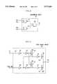
- FIG. 1shows the configuration of a semiconductor memory relating to an embodiment of the invention.
- FIG. 2is a circuit diagram showing the configuration of the coincidence circuit in FIG. 1.
- FIG. 3is a circuit diagram showing the configuration of the data output circuit in FIG. 1.
- FIG. 4is a timing chart of the condition for a shift to the test mode.
- FIG. 1shows the configuration of the main part of the semiconductor memory relating to a preferred embodiment of the invention. The embodiment will be described, taking a DRAM as an example.
- the DRAMcomprises: a 16-memory array 11 having a plurality of memory cells; main amplifiers M1 to M16 provided for each bit in the memory array 11; input/output pads I/O 1 to 16 for each bit for data input and output; input/output buffers 13-1 to 13-16, each provided on an input/output bus 12 connecting the main amplifiers M1 to M16 and the I/O pads I/O 1 to I/O 16; and four test circuits 14-1 to 14-4.
- FIG. 1shows the test circuit 14-1 only and the other test circuits are omitted.
- Four of the I/O pads I/O 1 to I/O 16belong to one of four groups, from one end to the other, from 1 to 4, 5 to 8, 9 to 12 and 13 to 16.
- Each of the test circuits 14-1 to 14-4is provided for each of the four groups.
- each of the I/O pads I/O 1, I/O 5, I/O 9 and I/O 13 representing each groupis only connected to a test data terminal (not shown) of an IC tester while the other I/O pads are not connected to the terminal.
- the test circuit 14-1is provided for the output pads I/O 1 to I/O 4 comprising the first I/O pads group.
- the test circuit 14-1comprises: a test mode detection circuit 21 connected to the I/O buffer 13-1; test mode writing circuits 22-1 to 22-4 with the inputs thereof connected together to the I/O buffer 13-1 and each of the outputs thereof connected to the main amplifiers M1 to M4 respectively; a coincidence circuit 23 with the input connected to the main amplifiers M1 to M4; and a data output circuit 24 with one of the inputs thereof connected to the output of the coincidence circuit 23 and the other of the inputs connected to the main amplifier M1 and the output thereof connected to the I/O buffer 13-1.
- the inputs of the test mode detection circuit 21are part of address signals 15 to be inputted to the memory array 11 (A0 and A1) and control signals (/RAS,/CAS,/WE) wherein these signals branch into the test mode detection circuit 21.
- the test mode detection circuit 21detects the DRAM having shifted to the test mode when these signals meet a given condition.
- Each of the test mode writing circuits 22-1 to 22-4is a buffer driver for writing an inputted data from the I/O pad I/O 1 into four memory cells of the memory army 11 at the same time.
- the coincidence circuit 23determines whether the data read from the four memory cells of the memory array 11 agree with each other to output a judging signal.
- the coincidence circuit 23may be configured with a circuit described hereinafter (FIG. 2).
- the data output circuit 24outputs the test result into the I/O buffer 13-1 based on the judging signal from the coincidence circuit 23.
- the data output circuit 24may be configured with a circuit described hereinafter (FIG. 3).
- FIG. 2shows the configuration of the coincidence circuit 23 in FIG. 1.
- the coincidence circuit 23comprises: an EX-NOR circuit 31 wherein the outputs of the main amplifiers M1 and M2 are inputted; an EX-NOR circuit 32 wherein the outputs of the main amplifiers M3 and M4 are inputted; an AND circuit 33 wherein the outputs of the EX-NOR circuits 31 and 32 are inputted.
- the AND circuit 33outputs a logic ⁇ 1 ⁇ as a judging signal 34 when all of the outputs from the main amplifiers M1 to M4 are ⁇ 0 ⁇ or ⁇ 1 ⁇ coincidentally. Otherwise, the AND circuit 33 outputs ⁇ 0 ⁇ .
- FIG. 3shows the configuration of the data output circuit 24 in FIG. 1.
- the data output circuit 234comprises: inverters 42 and 43 connected in series to an input terminal 41 to which the judging signal 34 is inputted; pMOS transistors 44 and 45 whose gates are connected to the output of the inverter 43 and whose sources are connected to a power source; an inverter 48 connected to the output of the main amplifier M1; inverters 49 and 50 connected in parallel to the output of the inverter 48; an nMOS transistor 53 whose gate is connected to the output of the inverter 50 and whose drain is connected to the power source; and an nMOS transistor 52 whose gate is connected to the output of the inverter 51 and whose source is connected to ground.
- the drain of the pMOS transistor 44is connected to the input of the inverter 50.
- the drain of the pMOS transistor 45is connected to the input of the inverter 51.
- the drain of the nMOS transistor 52is connected to source of the nMOS transistor 53 and to the output 54 thereof.
- test circuits 14-2, 14-3 and 14-4are provided for each of the other (the second, third and fourth) groups of I/O pads, each including the I/O pads I/O 5 to I/O 8, I/O 9 to I/O 12 and I/O 13 to I/O 16 respectively.
- the test mode detection circuit 21detects given data set to particular two address lines in a CAS before RAS state and shifts to the test mode.
- two address signals A0 and A1, (d) and (e) in FIG. 4are set to ⁇ 0 ⁇ and ⁇ 1 ⁇ respectively and a signal /WE and a signal/CAS, (b) and (c) in FIG. 4, are active (low).
- a signal/RAS(a) in FIG. 4, goes active (low) at T1
- the test mode detection circuit 21detects it and recognizes that the DRAM has shifted to the test mode.
- an IC tester(not shown in the figures) inputs ⁇ 0 ⁇ or ⁇ 1 ⁇ as test data to the I/O pad I/O 1.
- the inputted datais then inputted to the main amplifiers M1 to M4 via the I/O buffer 13-1 and the test mode writing circuits 22-1 to 22-4, to be written into four memory cells in the memory array 11 simultaneously.
- test data inputted from each of the I/O pads I/O 5, I/O 9 and I/O 13is simultaneously written into four memory cells via the test mode writing circuit of each of the test circuits 14-2, 14-3 and 14-4 (not shown) respectively.
- Test data ( ⁇ 0 ⁇ or ⁇ 1 ⁇ ) simultaneously inputted from the I/O pads I/O 1, I/O 5, I/O 9 and I/O 13may be either the same or not.
- the written datawill be read out.
- the data read from the four memory cells of the memory array 11is inputted to the coincidence circuit 23 via the main amplifiers M1 to M4.
- the coincidence circuit 23determines whether the four data agree with each other or not and outputs the result to the data output circuit 24.
- a logic ⁇ 1 ⁇is outputted as the judging signal 34 when all the data is ⁇ 0 ⁇ or ⁇ 1 ⁇ to coincide with each other. Otherwise, ⁇ 0 ⁇ is outputted.
- a judging signal ⁇ 1 ⁇is inputted to the input terminal 41 of the data output terminal 24 in FIG. 3 so as to turn off both pMOS transistors 44 and 45. If all of the four data is ⁇ 1 ⁇ , data ⁇ 1 ⁇ is inputted from the main amplifier M1 so as to turn off the transistor 52 and to turn on the transistor 53, and data ⁇ 1 ⁇ is outputted from the output terminal 54. If all of the four data is ⁇ 0 ⁇ , data ⁇ 0 ⁇ is inputted from the main amplifier M1 so as to turn on the transistor 52 and to turn off the transistor 53, and data ⁇ 0 ⁇ is outputted from the output terminal 54.
- a judging signal ⁇ 0 ⁇is inputted to the input terminal 41 of the data output terminal 24 in FIG. 3 so as to turn on both pMOS transistors 44 and 45.
- both nMOS transistors 52 and 53turn off and the impedance at the output terminal 54 goes high.
- the data result outputted from the data output circuit 24is outputted from the I/O pad I/O 1 via the I/O buffer 13-1.
- the IC tester(not shown) determines whether the four memory cells tested pass or fail based on the data result. That is, when the data result is ⁇ 1 ⁇ , data ⁇ 1 ⁇ is read from all of the four memory cells where data ⁇ 1 ⁇ is written so that the written data coincides with the read data. When the data result is ⁇ 0 ⁇ , data ⁇ 0 ⁇ is read from all of the four memory cells where data ⁇ 0 ⁇ is written so that the written data coincides with the read data. When the data result is of high impedance, it is determined that the data do not coincide, that is, a memory error (a writing or a reading error) has occurred.
- each of the other test circuits 14-2 to 14-4outputs the data result for the four memory cells to be inputted to the IC tester via each of the I/O pads I/O 5, I/O 9 and I/O 13.
- the IC testerdetermines whether each of the four memory cells being tested pass or fail.
- This embodimentthus allows only four of the sixteen I/O pads to test all the memory cells so as to determine the quality of the chip. As a result, the number of memory chips to be tested is effectively increased for a multiple-bit DRAM of 16 bits.
- a shift to the test modeis detected when the state shifts to the CAS before RAS while the address signals A0 to A1 are set to the given values.
- a condition for a shift to the test modemay be an application of a voltage (like 10V) higher than normal power supply (3 to 5V) to a particular signal, for example, at least one of the control signals like/RAS,/CAS,/WE,/OE and the address signal.
- a voltagelike 10V
- normal power supply3 to 5V
- the control signalslike/RAS,/CAS,/WE,/OE and the address signal.
- only the particular signalneed be inputted to the test mode detection circuit 21 besides the memory array 11.
- the present inventionis not limited to a 16-bit DRAM.
- an 8-bit DRAMfor example, four of the I/O pads I/O 1, I/O 3, I/O 5 and I/O 7 are used wherein two memory cells are tested through one of the I/O pads.
- a 32-bit DRAMfour of the I/O pads I/O 1, I/O 9, I/O 17 and I/O 25 are used wherein eight memory cells are tested through one of the I/O pads.
- the inventionis not limited to a DRAM but may be applied to other semiconductor memories such as a SRAM, ROM, EEPROM and flash memory
Landscapes
- For Increasing The Reliability Of Semiconductor Memories (AREA)
- Dram (AREA)
- Tests Of Electronic Circuits (AREA)
Abstract
Description
Claims (6)
Applications Claiming Priority (2)
| Application Number | Priority Date | Filing Date | Title |
|---|---|---|---|
| JP7-266223 | 1995-09-20 | ||
| JP7266223AJPH0991998A (en) | 1995-09-20 | 1995-09-20 | Semiconductor memory |
Publications (1)
| Publication Number | Publication Date |
|---|---|
| US5717643Atrue US5717643A (en) | 1998-02-10 |
Family
ID=17427982
Family Applications (1)
| Application Number | Title | Priority Date | Filing Date |
|---|---|---|---|
| US08/715,069Expired - LifetimeUS5717643A (en) | 1995-09-20 | 1996-09-19 | Semiconductor memory device with testing function |
Country Status (3)
| Country | Link |
|---|---|
| US (1) | US5717643A (en) |
| JP (1) | JPH0991998A (en) |
| KR (1) | KR970018600A (en) |
Cited By (11)
| Publication number | Priority date | Publication date | Assignee | Title |
|---|---|---|---|---|
| US5862146A (en)* | 1997-04-15 | 1999-01-19 | Texas Instruments Incorporated | Process of testing memory parts and equipment for conducting the testing |
| US5926422A (en)* | 1997-10-02 | 1999-07-20 | Texas Instruments Incorporated | Integrated circuit memory device having current-mode data compression test mode |
| US5933378A (en)* | 1998-02-26 | 1999-08-03 | Micron Technology, Inc. | Integrated circuit having forced substrate test mode with improved substrate isolation |
| US6009026A (en)* | 1997-07-28 | 1999-12-28 | International Business Machines Corporation | Compressed input/output test mode |
| US6038182A (en)* | 1998-02-02 | 2000-03-14 | Samsung Electronics Co., Ltd. | Integrated circuit memory devices and testing methods including selectable input/output channels |
| KR100425444B1 (en)* | 2001-03-27 | 2004-03-30 | 삼성전자주식회사 | Semiconductor memory device including chip selection circuit and method for generating chip selection signal |
| US20040208365A1 (en)* | 2003-04-15 | 2004-10-21 | Loui Alexander C. | Method for automatically classifying images into events |
| US20040208377A1 (en)* | 2003-04-15 | 2004-10-21 | Loui Alexander C. | Method for automatically classifying images into events in a multimedia authoring application |
| US20070079271A1 (en)* | 2005-09-21 | 2007-04-05 | Fujitsu Limited | Design tool, design method, and program for semiconductor device |
| US8078618B2 (en) | 2006-01-30 | 2011-12-13 | Eastman Kodak Company | Automatic multimode system for organizing and retrieving content data files |
| US12367944B2 (en)* | 2022-11-01 | 2025-07-22 | Samsung Electronics Co., Ltd. | Memory device including test pad connection circuit |
Families Citing this family (11)
| Publication number | Priority date | Publication date | Assignee | Title |
|---|---|---|---|---|
| KR100480568B1 (en)* | 1997-10-27 | 2005-09-30 | 삼성전자주식회사 | Super voltage detector, semiconductor memory device & mode setting |
| JPH11317100A (en) | 1998-05-06 | 1999-11-16 | Mitsubishi Electric Corp | Semiconductor storage device |
| KR100408395B1 (en) | 2001-01-26 | 2003-12-06 | 삼성전자주식회사 | Test system and method for effectively testing semiconductor device having lots of pins |
| JP3925839B2 (en)* | 2001-09-10 | 2007-06-06 | シャープ株式会社 | Semiconductor memory device and test method thereof |
| JP3943890B2 (en)* | 2001-10-18 | 2007-07-11 | 富士通株式会社 | Semiconductor device |
| US6639859B2 (en)* | 2001-10-25 | 2003-10-28 | Hewlett-Packard Development Company, L.P. | Test array and method for testing memory arrays |
| JP2003168300A (en)* | 2001-11-29 | 2003-06-13 | Mitsubishi Electric Corp | Semiconductor device |
| KR100660538B1 (en)* | 2004-06-30 | 2006-12-22 | 삼성전자주식회사 | Semiconductor memory device |
| JP4562468B2 (en)* | 2004-09-13 | 2010-10-13 | ルネサスエレクトロニクス株式会社 | Semiconductor memory device |
| JP2007272982A (en)* | 2006-03-31 | 2007-10-18 | Matsushita Electric Ind Co Ltd | Semiconductor memory device and inspection method thereof |
| JP2009070456A (en)* | 2007-09-12 | 2009-04-02 | Renesas Technology Corp | Semiconductor storage device |
Citations (3)
| Publication number | Priority date | Publication date | Assignee | Title |
|---|---|---|---|---|
| US5228000A (en)* | 1990-08-02 | 1993-07-13 | Mitsubishi Denki Kabushiki Kaisha | Test circuit of semiconductor memory device |
| US5400281A (en)* | 1991-06-27 | 1995-03-21 | Nec Corporation | Static random access memory device with memory cell testing circuit |
| US5615166A (en)* | 1994-05-17 | 1997-03-25 | Seiko Instruments Inc. | Semiconductor memory integrated circuit |
- 1995
- 1995-09-20JPJP7266223Apatent/JPH0991998A/enactivePending
- 1996
- 1996-09-10KRKR1019960039154Apatent/KR970018600A/ennot_activeCeased
- 1996-09-19USUS08/715,069patent/US5717643A/ennot_activeExpired - Lifetime
Patent Citations (3)
| Publication number | Priority date | Publication date | Assignee | Title |
|---|---|---|---|---|
| US5228000A (en)* | 1990-08-02 | 1993-07-13 | Mitsubishi Denki Kabushiki Kaisha | Test circuit of semiconductor memory device |
| US5400281A (en)* | 1991-06-27 | 1995-03-21 | Nec Corporation | Static random access memory device with memory cell testing circuit |
| US5615166A (en)* | 1994-05-17 | 1997-03-25 | Seiko Instruments Inc. | Semiconductor memory integrated circuit |
Cited By (13)
| Publication number | Priority date | Publication date | Assignee | Title |
|---|---|---|---|---|
| US5862146A (en)* | 1997-04-15 | 1999-01-19 | Texas Instruments Incorporated | Process of testing memory parts and equipment for conducting the testing |
| US6009026A (en)* | 1997-07-28 | 1999-12-28 | International Business Machines Corporation | Compressed input/output test mode |
| US5926422A (en)* | 1997-10-02 | 1999-07-20 | Texas Instruments Incorporated | Integrated circuit memory device having current-mode data compression test mode |
| US6038182A (en)* | 1998-02-02 | 2000-03-14 | Samsung Electronics Co., Ltd. | Integrated circuit memory devices and testing methods including selectable input/output channels |
| US5933378A (en)* | 1998-02-26 | 1999-08-03 | Micron Technology, Inc. | Integrated circuit having forced substrate test mode with improved substrate isolation |
| US6388926B1 (en) | 1998-02-26 | 2002-05-14 | Micron Technology, Inc. | Integrated circuit having forced substrate test mode with improved substrate isolation |
| KR100425444B1 (en)* | 2001-03-27 | 2004-03-30 | 삼성전자주식회사 | Semiconductor memory device including chip selection circuit and method for generating chip selection signal |
| US20040208365A1 (en)* | 2003-04-15 | 2004-10-21 | Loui Alexander C. | Method for automatically classifying images into events |
| US20040208377A1 (en)* | 2003-04-15 | 2004-10-21 | Loui Alexander C. | Method for automatically classifying images into events in a multimedia authoring application |
| US6865297B2 (en) | 2003-04-15 | 2005-03-08 | Eastman Kodak Company | Method for automatically classifying images into events in a multimedia authoring application |
| US20070079271A1 (en)* | 2005-09-21 | 2007-04-05 | Fujitsu Limited | Design tool, design method, and program for semiconductor device |
| US8078618B2 (en) | 2006-01-30 | 2011-12-13 | Eastman Kodak Company | Automatic multimode system for organizing and retrieving content data files |
| US12367944B2 (en)* | 2022-11-01 | 2025-07-22 | Samsung Electronics Co., Ltd. | Memory device including test pad connection circuit |
Also Published As
| Publication number | Publication date |
|---|---|
| JPH0991998A (en) | 1997-04-04 |
| KR970018600A (en) | 1997-04-30 |
Similar Documents
| Publication | Publication Date | Title |
|---|---|---|
| US5717643A (en) | Semiconductor memory device with testing function | |
| EP0615251B1 (en) | Semiconductor memory with built-in parallel bit test mode | |
| US7136316B2 (en) | Method and apparatus for data compression in memory devices | |
| US4916700A (en) | Semiconductor storage device | |
| KR100374312B1 (en) | Semiconductor memory device with output data scramble circuit | |
| US6323664B1 (en) | Semiconductor memory device capable of accurately testing for defective memory cells at a wafer level | |
| US6687174B2 (en) | Semiconductor memory device capable of switching output data width | |
| KR100356091B1 (en) | Semiconductor memory and memory system | |
| US6484289B1 (en) | Parallel data test for a semiconductor memory | |
| KR100392674B1 (en) | Semiconductor memory | |
| US6731553B2 (en) | Memory circuit having compressed testing function | |
| US5654924A (en) | Semiconductor memory device capable of operating with potentials of adjacent bit lines inverted during multi-bit test | |
| KR100192590B1 (en) | Parallel bit test circuit for semiconductor memory device | |
| US6317373B1 (en) | Semiconductor memory device having a test mode and semiconductor testing method utilizing the same | |
| JPH08203278A (en) | Semiconductor memory | |
| US5812470A (en) | Apparatus, system and method for identifying semiconductor memory access modes | |
| KR100346447B1 (en) | Apparatus for Parallel Testing in Semiconductor Memory Device | |
| KR100209335B1 (en) | Memory Cell Stress Applied Device | |
| JPS63140499A (en) | Semiconductor memory device | |
| JPH03237698A (en) | Test circuit for semiconductor memory | |
| JPH04313900A (en) | Semiconductor storage device | |
| JPH05101699A (en) | Memory device | |
| KR19990043663A (en) | Parallel bit test circuit of semiconductor memory device | |
| JPH0845300A (en) | Semiconductor memory device and test method thereof |
Legal Events
| Date | Code | Title | Description |
|---|---|---|---|
| AS | Assignment | Owner name:NIPPON STEEL SEMICONDUCTOR CORPORATION, JAPAN Free format text:ASSIGNMENT OF ASSIGNORS INTEREST;ASSIGNORS:IWANAMI, EIICHI;WADA, TOSHIO;REEL/FRAME:008229/0866 Effective date:19960828 | |
| STCF | Information on status: patent grant | Free format text:PATENTED CASE | |
| FPAY | Fee payment | Year of fee payment:4 | |
| REMI | Maintenance fee reminder mailed | ||
| FPAY | Fee payment | Year of fee payment:8 | |
| SULP | Surcharge for late payment | Year of fee payment:7 | |
| FPAY | Fee payment | Year of fee payment:12 | |
| AS | Assignment | Owner name:NIPPON FOUNDRY INC., JAPAN Free format text:CHANGE OF NAME;ASSIGNOR:NIPPON STEEL SEMICONDUCTOR CORPORATION;REEL/FRAME:029700/0148 Effective date:20130127 | |
| AS | Assignment | Owner name:UMC JAPAN, JAPAN Free format text:CHANGE OF NAME;ASSIGNOR:NIPPON FOUNDRY INC.;REEL/FRAME:029736/0336 Effective date:20130131 | |
| AS | Assignment | Owner name:UNITED MICROELECTRONICS CORP., TAIWAN Free format text:ASSIGNMENT OF ASSIGNORS INTEREST;ASSIGNOR:UMC JAPAN;REEL/FRAME:029820/0811 Effective date:20121201 |