US5716875A - Method for making a ferroelectric device - Google Patents
Method for making a ferroelectric deviceDownload PDFInfo
- Publication number
- US5716875A US5716875AUS08/609,697US60969796AUS5716875AUS 5716875 AUS5716875 AUS 5716875AUS 60969796 AUS60969796 AUS 60969796AUS 5716875 AUS5716875 AUS 5716875A
- Authority
- US
- United States
- Prior art keywords
- ferroelectric
- forming
- transistors
- substrate
- barrier layer
- Prior art date
- Legal status (The legal status is an assumption and is not a legal conclusion. Google has not performed a legal analysis and makes no representation as to the accuracy of the status listed.)
- Expired - Lifetime
Links
Images


Classifications
- H—ELECTRICITY
- H10—SEMICONDUCTOR DEVICES; ELECTRIC SOLID-STATE DEVICES NOT OTHERWISE PROVIDED FOR
- H10B—ELECTRONIC MEMORY DEVICES
- H10B53/00—Ferroelectric RAM [FeRAM] devices comprising ferroelectric memory capacitors
- H—ELECTRICITY
- H10—SEMICONDUCTOR DEVICES; ELECTRIC SOLID-STATE DEVICES NOT OTHERWISE PROVIDED FOR
- H10B—ELECTRONIC MEMORY DEVICES
- H10B53/00—Ferroelectric RAM [FeRAM] devices comprising ferroelectric memory capacitors
- H10B53/30—Ferroelectric RAM [FeRAM] devices comprising ferroelectric memory capacitors characterised by the memory core region
- H—ELECTRICITY
- H10—SEMICONDUCTOR DEVICES; ELECTRIC SOLID-STATE DEVICES NOT OTHERWISE PROVIDED FOR
- H10D—INORGANIC ELECTRIC SEMICONDUCTOR DEVICES
- H10D1/00—Resistors, capacitors or inductors
- H10D1/60—Capacitors
- H10D1/68—Capacitors having no potential barriers
- H10D1/682—Capacitors having no potential barriers having dielectrics comprising perovskite structures
- H—ELECTRICITY
- H10—SEMICONDUCTOR DEVICES; ELECTRIC SOLID-STATE DEVICES NOT OTHERWISE PROVIDED FOR
- H10D—INORGANIC ELECTRIC SEMICONDUCTOR DEVICES
- H10D84/00—Integrated devices formed in or on semiconductor substrates that comprise only semiconducting layers, e.g. on Si wafers or on GaAs-on-Si wafers
- H10D84/01—Manufacture or treatment
- H10D84/0123—Integrating together multiple components covered by H10D12/00 or H10D30/00, e.g. integrating multiple IGBTs
- H10D84/0126—Integrating together multiple components covered by H10D12/00 or H10D30/00, e.g. integrating multiple IGBTs the components including insulated gates, e.g. IGFETs
- H10D84/0165—Integrating together multiple components covered by H10D12/00 or H10D30/00, e.g. integrating multiple IGBTs the components including insulated gates, e.g. IGFETs the components including complementary IGFETs, e.g. CMOS devices
- H—ELECTRICITY
- H10—SEMICONDUCTOR DEVICES; ELECTRIC SOLID-STATE DEVICES NOT OTHERWISE PROVIDED FOR
- H10D—INORGANIC ELECTRIC SEMICONDUCTOR DEVICES
- H10D84/00—Integrated devices formed in or on semiconductor substrates that comprise only semiconducting layers, e.g. on Si wafers or on GaAs-on-Si wafers
- H10D84/01—Manufacture or treatment
- H10D84/02—Manufacture or treatment characterised by using material-based technologies
- H10D84/03—Manufacture or treatment characterised by using material-based technologies using Group IV technology, e.g. silicon technology or silicon-carbide [SiC] technology
- H10D84/038—Manufacture or treatment characterised by using material-based technologies using Group IV technology, e.g. silicon technology or silicon-carbide [SiC] technology using silicon technology, e.g. SiGe
- H—ELECTRICITY
- H10—SEMICONDUCTOR DEVICES; ELECTRIC SOLID-STATE DEVICES NOT OTHERWISE PROVIDED FOR
- H10D—INORGANIC ELECTRIC SEMICONDUCTOR DEVICES
- H10D84/00—Integrated devices formed in or on semiconductor substrates that comprise only semiconducting layers, e.g. on Si wafers or on GaAs-on-Si wafers
- H10D84/80—Integrated devices formed in or on semiconductor substrates that comprise only semiconducting layers, e.g. on Si wafers or on GaAs-on-Si wafers characterised by the integration of at least one component covered by groups H10D12/00 or H10D30/00, e.g. integration of IGFETs
- H10D84/811—Combinations of field-effect devices and one or more diodes, capacitors or resistors
- H—ELECTRICITY
- H10—SEMICONDUCTOR DEVICES; ELECTRIC SOLID-STATE DEVICES NOT OTHERWISE PROVIDED FOR
- H10D—INORGANIC ELECTRIC SEMICONDUCTOR DEVICES
- H10D88/00—Three-dimensional [3D] integrated devices
- H—ELECTRICITY
- H10—SEMICONDUCTOR DEVICES; ELECTRIC SOLID-STATE DEVICES NOT OTHERWISE PROVIDED FOR
- H10D—INORGANIC ELECTRIC SEMICONDUCTOR DEVICES
- H10D88/00—Three-dimensional [3D] integrated devices
- H10D88/01—Manufacture or treatment
Definitions
- the present inventionrelates generally to semiconductor processing, and more particularly, to forming ferroelectric memory devices on semiconductor wafers.
- Ferroelectric memory cells and microcontrollers which contain ferroelectric memory portionsare currently being manufactured or considered for high volume production.
- the PMOS and/or NMOS transistorsare usually exposed to a hydrogen anneal process.
- This hydrogen anneal processneutralizes dangling bonds and reduces surface charge problems at the substrate-to-gate-oxide interface of the PMOS and/or NMOS transistors. Therefore, the hydrogen anneal greatly enhances transistor yield, where electrical breakdown of gate dielectrics are reduced and threshold voltage (Vt) shifts are mimimized.
- Vtthreshold voltage
- the hydrogen anneal processincorporates hydrogen into the substrate and this hydrogen anneal is damaging to the deposited ferroelectric material.
- a hydrogen annealmay be used to improve the yield of CMOS transistors, however, this anneal process creates a yield reduction in the ferroelectric capacitors which overlie the CMOS transistors.
- the total yield of the ICis probably not significantly improved by the hydrogen anneal and the yield may even be reduced when using a conventional transistor hydrogen anneal methodology due to increased ferroelectric failure rates.
- an oxygen annealmay be used to improve the yield of ferroelectric capacitors.
- an oxygen annealcan typically damage underlying PMOS and NMOS transistors. Therefore, if hydrogen anneal processes are used as known in the prior art, CMOS transistors in the substrate are improved in yield while ferroelectric capacitors overlying the transistors are damaged.
- the ferroelectric capacitorsare improved in yield while the transistors within the substrate are either damaged or not properly annealed to remove transistor process damage so that the yield of the transistors are inadequate.
- FIGS. 1-14illustrate, in cross sectional diagrams, a method for forming a ferroelectric cell in accordance with the present invention.
- the present inventionis a method for manufacturing a ferroelectric memory device and a resulting ferroelectric memory structure.
- the ferroelectric processbegins by manufacturing N-type and P-type CMOS transistor structures in a substrate.
- the CMOS transistorsare then annealed in a hydrogen anneal at roughly 390° C. (typically a temperature between 200° C. and 500° C. is used).
- the hydrogen annealinvolves exposing the wafers to an ambient that contains 4-5% hydrogen and a remainder nitrogen.
- the hydrogen annealis performed after manufacturing the CMOS transistors in order to neutralize dangling bonds or Qss charge at the silicon-gate oxide interface near polysilicon gate electrodes.
- CMOS transistorsThis reduction of dangling bonds at the gate oxide/substrate interface of CMOS transistors stabilizes threshold voltages (Vt) and increases yield of the transistors.
- a silicon nitride layerwhich is typically 450 angstroms thick is deposited. This silicon nitride layer is deposited on the backside of the wafer as well as the front side of the wafer.
- the silicon nitride layercontains the hydrogen atoms from the hydrogen anneal to the CMOS transistors and surrounding layers for transistor yield improvement while preventing the hydrogen from out-defusing and damaging subsequent ferroelectric processing.
- ferroelectric capacitor processingbegins.
- a strontium bismuth tantalum oxideis used as the ferroelectric dielectric for a ferroelectric capacitor which overlies the CMOS transistors.
- Strontium bismuth tantalum oxideis typically denoted as Y1 and has the chemical symbol SrBi 2 Ta 2 O 9 . It is important to note that other ferroelectric materials may be used as the ferroelectric capacitor material.
- Contact openingsare then etched to the electrodes of the ferroelectric capacitor and the transistors formed on the substrate.
- a tantalum nitride barrieris deposited for the first metallic layer of aluminum (typically 98%/1%/1% aluminum/silicon/copper) that will fill these contact openings.
- the tantalum nitrideis used as a barrier between the platinum electrodes of the ferroelectric capacitor and aluminum.
- the tantalum nitrideis also used as a barrier between aluminum and silicon substrate material.
- the tantalum nitridewill further encapsulate the hydrogen from the transistor hydrogen anneal previously discussed to the transistor areas and keep the hydrogen anneal from affecting subsequent ferroelectric processing.
- an oxygen annealis performed to crystalize the ferroelectric material.
- An oxygen annealis required in order to cure defects and damage in the ferroelectric material to increase the yield of the ferroelectric material and improve operation of the ferroelectric device.
- a typical oxygen annealoccurs at 400° C. (between 300° C. and 500° C.) and the ambient is pure oxygen (O 2 ).
- the silicon nitride layer and tantalum nitride barrierwhich were previously deposited and discussed above are used to separate the effects of the hydrogen anneal from the effects of the oxygen anneal.
- the silicon nitride layercontains all of the hydrogen advantages of the hydrogen anneal to the CMOS transistors while preventing hydrogen from damaging the ferroelectric capacitor array which overlies the CMOS transistors.
- the silicon nitride layerallows the oxygen anneal to improve the performance of the ferroelectric capacitors while not allowing the oxygen anneal to damage the underlying CMOS transistors.
- a ferroelectric device containing optimized transistors via a hydrogen anneal and optimized ferroelectric capacitors via an oxygen annealcan be formed on a single substrate where the detrimental effects of transistor performance via oxygen anneals are avoided and the detrimental effects to ferroelectric materials via hydrogen anneals are avoided.
- the resulting productis a high yield, high performance CMOS ferroelectric product that has not yet been manufactured in the integrated circuit industry.
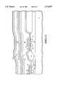
- FIG. 1illustrates the beginning of a process used to form a ferroelectric integrated circuit having high performance and high yield.
- a substrate 10is provided.
- substrate 10is a N-type silicon semiconductor wafer.
- the substrate 10may be a silicon on insulator (SOI) substrate, a gallium arsenide substrate, a germanium doped substrate, either an N-type or a P-type silicon wafer, a wafer bonded substrate, or any like semiconductor wafer starting material.
- SOIsilicon on insulator
- the wafersare laser scribed with an identification number for manufacturing identification.
- a thin oxide layer(not specifically illustrated in FIG. 1) is formed followed by the deposition of a thicker nitride layer 12.
- a photoresist layer 14is spun on top of the silicon nitride layer 12.
- the photoresist layer 14is exposed to light and chemically developed selectively via a lithographic masking process.
- An etch procedureis then used to etch away portions of the silicon nitride layer 12 exposed by the developed photoresist layer 14.
- An N-type ion implant stepis used to implant phosphorous within exposed regions of the substrate 10 to form an N doped region of the substrate 10 referred to as doped region 16.
- a typical implant process for forming the region 16occurs between 80 Kev and 120 Kev and involves phosphorous implantation at a surface area dose on the order of 1 ⁇ 10 13 atoms/cm 2 .
- FIG. 2illustrates that the photoresist layer 14 is stripped from the substrate via an ash process.
- a top surface of the region 16is oxidized via a thermal oxide growth process illustrated in FIG. 2.
- the thermal oxide growth processresults in a thick 2,500-4,500 angstrom well oxide region 18.
- Phosphorous in the region 16will "snowplow" underneath the oxide portion 18, meaning that the segregation coefficient of phosphorus into oxide is such that the phosphorus resists being consumed by the oxide and instead piles up at the interface of the oxide/silicon growth region.
- the nitride layer 12is etched via known nitride etch processing.
- the layer 18is then used as an implant mask to ion implant boron into the substrate 10 to form a boron doped region 20.
- Typical energy for the boron implantis between 25 Kev and 45 Kev and the dose implanted is on the order of 1 ⁇ 10 12 atoms/cm 2 to 1 ⁇ 10 13 atoms/cm 2 .
- FIG. 3illustrates that a thermal well drive process is used to thermally drive/diffuse the dopant atoms in regions 16 and 20 deeper into the substrate to form N-well region 16 and P-well region 20.
- the oxide layer 18is exposed to an etch environment and removed from the substrate 10.
- a 300-650 angstrom oxide layer 22is formed overlying the well regions 16 and 20.
- a 1,200 to 1,800 angstrom silicon nitride layer 24is deposited overlying the layer 22.
- Photoresist 26is spun on the wafer and patterned as indicated in FIG. 3. Exposed portions of layers 24 and 22 which overlie an interface region of the wells 16 and 20 are etched as illustrated in FIG. 3. After the etching of the openings through layers 22 and 24, the photoresist 26 is stripped via an ash process in FIG. 4.
- FIG. 4another photoresist layer 30 is deposited on the substrate and patterned as illustrated in FIG. 4. Photoresist 30 and layers 24-22 are then used as a hard/soft masking area for an ion implantation step which implants boron to form a region 28 within well 20.
- the ion implant step used to form the region 28is a low energy implant which places 1 ⁇ 10 13 to 1 ⁇ 10 14 boron atoms per centimeter squared into a field oxide isolation region of the P-well 20.
- the photoresist layer 30is stripped from the substrate, and field oxide region 32 is grown in the opening of layers 24 and 22.
- the presence of the silicon nitride layer 24limits the effects of birds beak in the oxide region 32 illustrated in FIG. 5.
- a typical thickness for the field oxide isolation region 32is within a range of roughly 5,000 angstroms to 10,000 angstroms in thickness.
- FIG. 6illustrates that a gate oxide 34 is formed.
- Gate oxidemay be a composite dielectric layer of tetraethylorthosilicate (TEOS) oxide and thermal oxide or may be a single thermal oxide layer of roughly 40 angstroms to 150 angstroms in thickness.
- the layer 34is a gate oxide layer which may be nitrided, fluorinated, or exposed to chlorine to enhance gate oxide performance. It is important to note that a sacrificial gate oxide process may be performed prior to the formation of gate oxide 34 to ensure a cleaner substrate surface prior to gate oxide formation.
- gate poly A(referred to also as A polysilicon) is formed via layer 36 in FIG. 6.
- a typical thickness for the layer of A polysilicon of a gate electrodeis between 300 angstroms and 650 angstroms in thickness.
- a photoresist layer 38is deposited and patterned as illustrated.
- the photoresist layer 38is used as a masking layer for an ion implant step of boron which forms a doped region 40 within the well 20.
- the implant step to form the region 40is typically of low energy and will typically implant boron into the P-well array as a threshold voltage (Vt) adjust measure.
- Vtthreshold voltage
- a second, higher energy boron implantis then performed to form punch-through protection regions within the well 20.
- the punch-through high energy implantis used to provide a high dose of boron around source and drain regions in the well 20 so that depletion regions around source and drain electrodes are reduced and avoid punch-through leakage phenomenon and known short channel effects.
- FIG. 7illustrates that the photoresist layer 38 is removed from the substrate and that B polysilicon is deposited onto the A polysilicon layer 36.
- the B polysilicon layer 38is typically thicker than the A polysilicon layer 36 and is between 2,250-3,500 angstroms in thickness.
- the polysilicon layers 36 and 38contact to form a single polysilicon gate electrode layer where the only evidence of dual layer A/B deposition is a continuous crystalline boundary separating the A/B polysilicon layers.
- the layers 36 and 38can be doped insitu during deposition or may be ion implanted with dopants after deposition to provide for a proper gate electrode conductivity.
- FIG. 8illustrates that the polysilicon layers 36 and 38 are lithographically patterned and etched to form gate electrodes 37a and 37b.
- the gate electrode 37aoverlies the P-well region 20 and the gate electrode 37b overlies the N-well region 16. Therefore, the gate electrode 37a is a gate electrode of an N-channel transistor and the gate electrode 37b is an electrode of a P-channel transistor.
- FIG. 8illustrates that a CMOS process is used to manufacture both N-channel and P-channel transistors on a single silicon substrate 10. After patterning and etching of the gate electrodes 37a and 37b, N-type lightly doped drain regions 40 are formed within well region 20 and lightly doped drain regions 42 doped with P-type dopants are formed within well 16. Therefore, regions 40 and 42 are lightly doped drain (LDD) regions for their respective transistors.
- LDDlightly doped drain
- FIG. 9illustrates that a silicon nitride layer is deposited and then etched to form silicon nitride spacers 44 laterally adjacent sidewalls of the gate electrodes 37a and 37b.
- a typical thickness for a silicon nitride layer when forming spacersis usually between 300 angstroms and 2,500 angstroms in thickness and the thickness deposited usually determines a base thickness of the spacer.
- a Tegal 901 or a like reactive ion etch (RIE) machinecan be used to etch the conformal silicon nitride layer into silicon nitride spacers 44 as illustrated in FIG. 9.
- an optional backside ash and/or etch and RTP processcan be used to perform gettering operations in the silicon substrate 10.
- the nitride spacers 44are used to self-align highly doped implants into the well regions 20 and 16 laterally adjacent the LDD regions to complete formation of the source and drain regions 40 and 42 of the CMOS transistors. While lightly doped drain (LDD) regions are typically formed with phosphorous and boron implants, highly doped drain (HDD) regions are typically formed with arsenic and BF 2 implants so that the HDD regions either thermally diffuse less than the LDD regions or be implanted shallower into the substrate. In FIG. 9, the formation of the CMOS transistors is structurally complete.
- FIG. 10illustrates that a 700 angstrom to 1,500 Angstrom TEOS layer 46 is deposited overlying the gate electrodes 37a and 37b.
- the CMOS transistorsare exposed to a 390° C. hydrogen anneal process wherein the wafers are exposed to an ambient containing 4-5% hydrogen and a remainder nitrogen (N 2 ).
- This hydrogen anneal processis advantageous for the transistors since the hydrogen will consume dangling bonds at the Si-SiO 2 interface between well region 20 and gate dielectric layer 34.
- dangling bonds between well region 16 and gate dielectric layer 34will be consumed underlying the gate electrode 37b. This consumption of dangling bonds will improve yield and stabilize threshold voltages (Vt) across the length of the wafer and the length of each IC on the wafer, thereby providing improved CMOS transistor operation.
- Vtthreshold voltages
- a 300-750 angstrom silicon nitride layer 48is deposited directly onto the TEOS layer 46 directly after a time when the hydrogen anneal is performed.
- the nitride layer 48is not only deposited overlying the gate electrodes 37a and 37b, but the silicon nitride layer 48 is deposited on the sidewalls of the wafer and the backside of the wafer substrate 10.
- LPCVDlow pressure chemical vapor deposition
- silicon nitride layer 48is deposited to contain the effects of the hydrogen anneal to the CMOS transistors while minimizing hydrogen anneal effects to all subsequent processing which is to occur in subsequent FIGS. 11-14.
- the deposition of nitride layer 48is followed with a 5,000 to 7,000 angstrom BPSG deposition and reflow process, which results in the BPSG layer 50 in FIG. 10.
- a 1,000 to 2,000 angstrom TEOS layer 52is deposited overlying the BPSG layer 50.
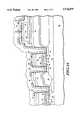
- FIG. 11illustrates the beginning of processing used to form ferroelectric capacitors which overlie the CMOS transistors.
- a 100 to 800 angstrom titanium layer 54is deposited on top of the 1,500 angstrom TEOS layer 52.
- a 650° C. O 2 30-minute oxidation processis then used to convert the 100-800 angstroms of titanium into approximately 175-1,400 angstroms of titanium dioxide which is illustrated in FIG. 11 by the layer 54.
- a 2,250 to 4,000 angstrom thick layer of platinumis then deposited as a layer 58, wherein layer 58 contacts the titanium oxide layer 54.
- a strontium bismuth tantalum oxide (Y1) or like ferroelectric materialis spun onto the wafer 58 to form a ferroelectric dielectric 60.
- an oxygen anneal processis performed to remove the organic content of the spin coat material and to crystallize the ferroelectric layer into the desired ferroelectric crystal phase.
- This oxygen annealis typically between 600° C. and 800° C. within a thermal exposure time range of at least one minute to many tens or hundreds of minutes.
- Other ferroelectric deposition techniquesare known and may be used, but all ferroelectric deposition techniques typically require a high temperature process or an anneal in an oxygen environment.
- a 1,500 to 3,000 Angstrom platinum layer 62is then deposited followed by a 100-300 angstrom titanium layer which is oxidized to form a titanium oxide layer 64 which is 175-525 angstroms thick. Therefore, layers 54 and 58 form a first ferroelectric capacitor electrode and layers 62 and 64 form a second ferroelectric capacitor electrode where layer 60 forms the capacitor dielectric wherein layer 60 is a ferroelectric material.
- FIG. 12indicates that a first photolithographic process is used to pattern and etch the top electrode comprising layers 62 and 64 and etch the ferroelectric material 60. It is important to note that the electrode comprising layers 62 and 64 may be etched in a step photolithographically different from the step used to etch layer 60 in a triple-tiered configuration ("wedding cake") manner. However, FIG. 12 illustrates that the top electric comprising layers 62 and 64 are self-aligned to the capacitor dielectric 60 etched in FIG. 12. A second photolithographic step is then used to define the layers 58 and 54 to leave behind a first electrode contact portion 65. Additionally, layers 58 and 54 can be patterned to connect a plurality of individual capacitors as appropriate for the particular circuit layout which is chosen. In essence, FIG. 12 illustrates that all of the layers 54 through 64 are lithographically patterned and etched to form individual capacitors for individual ferroelectric storage cells.
- FIG. 13illustrates that a 3,000 to 5,000 angstrom TEOS layer 66 is deposited. Openings are then formed through layer 66 to expose the first and second electrodes of the ferroelectric capacitor in FIG. 13.
- the layer 64will not be a good conductor and is etched away if at all possible to expose the platinum of layer 62 for superior electrical contact.
- the contact region 65is used to contact the bottom electrode or first electrode of the ferroelectric capacitor whereas contact is directly made to a capacitor electrode portion of layer 64 to contact the second electrode of the ferroelectric capacitor.
- FIG. 14illustrates that after the openings are formed to the capacitor in FIG. 13, a second photolithographic and etch process is then used to form openings through the layers 66, 52, 50, 48, 46, and 34 to expose source and drain regions 40 and 42 where exposure is needed in order to form electrical contacts. A similar set of contact holds are formed to contact the gate electrode 37a and 37b where these gate contacts are not illustrated in FIG. 14. After formation of all of the contact openings in FIG. 14, a tantalum nitride metal barrier layer 67 is deposited within the contact openings.
- the layer 67may be either total tantalum nitride, a first layer of titanium and a second layer of tantalum nitride, or a first layer of tantalum and a second layer of tantalum nitride.
- the layer 67may be made from any barrier material other than tantalum nitride, such as titanium nitride, tantalum, or titanium tungsten, however, tantalum nitride or a tantalum nitride composite is preferred.
- the formation of layer 57is followed by a 5,000 to 7,000 angstrom aluminum deposition to form an aluminum layer 68.
- the aluminum layeris typically a 98% Aluminum, 1% silicon, 1% copper alloy.
- a photolithographic processis used to pattern and etch the aluminum layer 68 and the tantalum nitride layer 67 into individual contact regions as illustrated in FIG. 14.
- FIG. 14illustrates that the transistor gate electrode 37a is coupled via one of these metal contact regions 67/68 to the ferroelectric capacitor formed near the right-hand side of FIG. 14. Therefore, the transistor gated gate electrode 37a and the capacitor illustrated in a right most portion of FIG. 14 are coupled together electrically to form a single ferroelectric memory cell in a configuration that is similar to the circuitry needed for a single transistor DRAM cell.
- the ferroelectric material 60requires an oxygen (O 2 ) anneal in order to repair mechanical and charge/plasma damage resulting in the ferroelectric material from all photolithographic, dielectric deposition, and etch processing occurring from FIG. 11 to FIG. 14.
- the substrateis submersed in a preferably pure O 2 environment at a temperature of 300° C. to 425° C. for roughly 30 minutes.
- Oxygen annealsare typically either detrimental to CMOS transistor operation or do not anneal transistor damage properly to increase transistor yield.
- the nitride layer 48 along with the barrier layer 67protects the CMOS devices gated by gates 37a and 37b from any damage from the oxygen anneal. Therefore, the ferroelectric material 60 can be cured optimally using an oxygen anneal while CMOS transistors are not detrimentally affected by this oxygen anneal process and instead maintain their hydrogen-annealed high yield.
- TEOS layer 70is deposited as passivation isolation. Holes are then etched through the passivation layer 70 to expose contact bond pads of the IC and formation of the integrated circuit is ready for conventional packaging and testing.
- FIGS. 1-14teach a method by which a hydrogen anneal may be used to increase yield and performance of CMOS transistors while not damaging ferroelectric material.
- an oxygen annealis used to benefit the ferroelectric material while not affecting adversely the operation of CMOS transistor arrays. Therefore, overall performance and yield of CMOS ferroelectric ICs are improved without adverse effects to any portion of the IC.
- any type of ferroelectric materialmay be used as the ferroelectric layer 60 in FIG. 14. More than one metal layer may be deposited on top of the substrate so that the process illustrated in FIGS. 1-14 may be integrated into a 2, 3, or 4 layer metal process. More than one layer of polysilicon may be deposited on the substrate to allow for the formation of both ferroelectric memory cells and other devices on the same substrate.
- Conductive electrodes of the capacitormay be replaced with other conductive material so that platinum and/or titanium need not be used. Titanium barriers and tantalum nitride barriers as taught herein may be interchanged and other conductive refractory metals and refractory metal oxides may be used as barrier layers. Dielectric layers as taught herein may be formed using any dielectric material.
- the hydrogen anneal taught hereinrecites that 4-5% hydrogen should be used, but it should be clear that any other concentration of hydrogen may be used, such as 3%-7%. Specific temperatures, times, thicknesses, doses, energies, etc. cited herein are preferred quantities and other quantities outside of the ranges cited herein as preferred may be used.
- ferroelectric materialsuch as lead zirconate titanate (PZT), barium titanate, calcium titanate, bismuth titanate, strontium titanate, lead zirconate, lead lanthanum zirconate titanate, lead niobium zirconate titanate, lead lanthanum niobium zirconate titanate, strontium bismuth tantalum oxide (Y1), strontium bismuth niobate, strontium bismuth niobate tantalate, barium strontium titanate, and/or lead titanate, either alone or in any combination may be used herein.
- PZTlead zirconate titanate
- barium titanatecalcium titanate
- bismuth titanatestrontium titanate
- strontium titanatelead zirconate, lead lanthanum zirconate titanate
- lead niobium zirconate titanatelead lanthanum niobium zirconate titanate
Landscapes
- Semiconductor Memories (AREA)
- Semiconductor Integrated Circuits (AREA)
Abstract
Description
Claims (28)
Priority Applications (3)
| Application Number | Priority Date | Filing Date | Title |
|---|---|---|---|
| US08/609,697US5716875A (en) | 1996-03-01 | 1996-03-01 | Method for making a ferroelectric device |
| JP05549697AJP4170409B2 (en) | 1996-03-01 | 1997-02-24 | Method for forming a semiconductor device |
| US08/959,554US6010927A (en) | 1996-03-01 | 1997-10-28 | Method for making a ferroelectric device having a tantalum nitride barrier layer |
Applications Claiming Priority (1)
| Application Number | Priority Date | Filing Date | Title |
|---|---|---|---|
| US08/609,697US5716875A (en) | 1996-03-01 | 1996-03-01 | Method for making a ferroelectric device |
Related Child Applications (1)
| Application Number | Title | Priority Date | Filing Date |
|---|---|---|---|
| US08/959,554DivisionUS6010927A (en) | 1996-03-01 | 1997-10-28 | Method for making a ferroelectric device having a tantalum nitride barrier layer |
Publications (1)
| Publication Number | Publication Date |
|---|---|
| US5716875Atrue US5716875A (en) | 1998-02-10 |
Family
ID=24441932
Family Applications (2)
| Application Number | Title | Priority Date | Filing Date |
|---|---|---|---|
| US08/609,697Expired - LifetimeUS5716875A (en) | 1996-03-01 | 1996-03-01 | Method for making a ferroelectric device |
| US08/959,554Expired - LifetimeUS6010927A (en) | 1996-03-01 | 1997-10-28 | Method for making a ferroelectric device having a tantalum nitride barrier layer |
Family Applications After (1)
| Application Number | Title | Priority Date | Filing Date |
|---|---|---|---|
| US08/959,554Expired - LifetimeUS6010927A (en) | 1996-03-01 | 1997-10-28 | Method for making a ferroelectric device having a tantalum nitride barrier layer |
Country Status (2)
| Country | Link |
|---|---|
| US (2) | US5716875A (en) |
| JP (1) | JP4170409B2 (en) |
Cited By (78)
| Publication number | Priority date | Publication date | Assignee | Title |
|---|---|---|---|---|
| US5837578A (en)* | 1997-02-24 | 1998-11-17 | Mosel Vitelic Inc. | Process of manufacturing a trenched stack-capacitor |
| US5893737A (en)* | 1995-04-26 | 1999-04-13 | Sharp Kabushiki Kaisha | Method for manufacturing semiconductor memory device |
| FR2776833A1 (en)* | 1998-03-30 | 1999-10-01 | Samsung Electronics Co Ltd | FERROELECTRIC CAPACITOR AND METHOD FOR MANUFACTURING A SEMICONDUCTOR DEVICE COMPRISING THE SAME |
| US5963466A (en)* | 1998-04-13 | 1999-10-05 | Radiant Technologies, Inc. | Ferroelectric memory having a common plate electrode |
| US6004839A (en)* | 1996-01-17 | 1999-12-21 | Nec Corporation | Semiconductor device with conductive plugs |
| FR2780812A1 (en)* | 1998-07-06 | 2000-01-07 | United Microelectronics Corp | METHOD FOR MANUFACTURING A DYNAMIC RAM MEMORY INCLUDED |
| US6037235A (en)* | 1998-09-14 | 2000-03-14 | Applied Materials, Inc. | Hydrogen anneal for curing defects of silicon/nitride interfaces of semiconductor devices |
| EP0996159A1 (en)* | 1998-10-12 | 2000-04-26 | STMicroelectronics S.r.l. | Integrated circuit structure comprising capacitor and corresponding manufacturing process |
| EP0996160A1 (en)* | 1998-10-12 | 2000-04-26 | STMicroelectronics S.r.l. | Contact structure for a semiconductor device |
| US6080617A (en)* | 1992-06-12 | 2000-06-27 | Matsushita Electric Industrial Co., Ltd. | Semiconductor device having capacitor and manufacturing method thereof |
| US6100100A (en)* | 1996-06-18 | 2000-08-08 | Matsushita Electronics Corporation | Method for manufacturing capacitor element |
| US6100150A (en)* | 1998-09-04 | 2000-08-08 | Taiwan Semiconductor Manufacturing Company | Process to improve temperature uniformity during RTA by deposition of in situ poly on the wafer backside |
| US6114199A (en)* | 1995-08-30 | 2000-09-05 | Sony Corporation | Manufacturing method for ferroelectric film and nonvolatile memory using the same |
| US6130103A (en)* | 1998-04-17 | 2000-10-10 | Symetrix Corporation | Method for fabricating ferroelectric integrated circuits |
| WO2000060646A1 (en)* | 1999-04-01 | 2000-10-12 | Infineon Technologies Ag | Method of processing a monocrystalline semiconductor disk and partially processed semiconductor disk |
| US6157979A (en)* | 1998-03-14 | 2000-12-05 | Advanced Technology Materials, Inc. | Programmable controlling device with non-volatile ferroelectric state-machines for restarting processor when power is restored with execution states retained in said non-volatile state-machines on power down |
| US6163043A (en)* | 1996-04-19 | 2000-12-19 | Matsushita Electronics Corp. | Semiconductor device |
| US6165802A (en)* | 1998-04-17 | 2000-12-26 | Symetrix Corporation | Method of fabricating ferroelectric integrated circuit using oxygen to inhibit and repair hydrogen degradation |
| US6175528B1 (en) | 1998-12-30 | 2001-01-16 | Hyundai Electronics Industries Co., Ltd. | Redundancy circuit and repair method for semiconductor memory device by utilizing ferroelectric memory |
| US6174735B1 (en) | 1998-10-23 | 2001-01-16 | Ramtron International Corporation | Method of manufacturing ferroelectric memory device useful for preventing hydrogen line degradation |
| US6194311B1 (en)* | 1998-06-26 | 2001-02-27 | Nec Corporation | Method for manufacturing semiconductor device capable of effectively carrying out hydrogen passivation |
| US6211542B1 (en)* | 1996-08-20 | 2001-04-03 | Ramtron International Corporation | Completely encapsulated top electrode of a ferroelectric capacitor using a lead-enhanced escapsulation layer |
| US6218218B1 (en)* | 1996-06-21 | 2001-04-17 | Texas Instruments Incorporated | Method for reducing gate oxide damage caused by charging |
| US6225656B1 (en) | 1998-12-01 | 2001-05-01 | Symetrix Corporation | Ferroelectric integrated circuit with protective layer incorporating oxygen and method for fabricating same |
| US6232131B1 (en)* | 1998-06-24 | 2001-05-15 | Matsushita Electronics Corporation | Method for manufacturing semiconductor device with ferroelectric capacitors including multiple annealing steps |
| US6242299B1 (en) | 1999-04-01 | 2001-06-05 | Ramtron International Corporation | Barrier layer to protect a ferroelectric capacitor after contact has been made to the capacitor electrode |
| US6249014B1 (en) | 1998-10-01 | 2001-06-19 | Ramtron International Corporation | Hydrogen barrier encapsulation techniques for the control of hydrogen induced degradation of ferroelectric capacitors in conjunction with multilevel metal processing for non-volatile integrated circuit memory devices |
| US6255122B1 (en) | 1999-04-27 | 2001-07-03 | International Business Machines Corporation | Amorphous dielectric capacitors on silicon |
| US6261917B1 (en) | 2000-05-09 | 2001-07-17 | Chartered Semiconductor Manufacturing Ltd. | High-K MOM capacitor |
| US6288433B1 (en) | 1997-12-18 | 2001-09-11 | Micron Technology, Inc. | Field effect transistor having improved hot carrier immunity |
| US6294805B1 (en)* | 1996-06-07 | 2001-09-25 | Samsung Electronics Co., Ltd. | Ferroelectric memory devices including capacitors located outside the active area and made with diffusion barrier layers |
| US6326258B1 (en)* | 1999-04-21 | 2001-12-04 | Nec Corporation | Method of manufacturing semiconductor device having thin film capacitor |
| US6333202B1 (en) | 1999-08-26 | 2001-12-25 | International Business Machines Corporation | Flip FERAM cell and method to form same |
| US6359295B2 (en) | 1997-09-29 | 2002-03-19 | Samsung Electronics Co., Ltd. | Ferroelectric memory devices including patterned conductive layers |
| US6388285B1 (en) | 1999-06-04 | 2002-05-14 | International Business Machines Corporation | Feram cell with internal oxygen source and method of oxygen release |
| US6391727B1 (en) | 1999-12-24 | 2002-05-21 | Hyundai Electronics Industries Co., Ltd. | Method of manufacturing a semiconductor device utilizing a(Al2O3)X-(TiO2)1-X gate dielectric film |
| US6395612B1 (en)* | 1997-10-31 | 2002-05-28 | Symetrix Corporation | Semiconductor device and method of manufacturing the same |
| US6399431B1 (en)* | 2000-03-21 | 2002-06-04 | Chartered Semiconductor Manufacturing Ltd. | ESD protection device for SOI technology |
| US20020098644A1 (en)* | 1998-11-17 | 2002-07-25 | Kabushiki Kaisha Toshiba | Semiconductor device and method for manufacturing the same |
| US20020127867A1 (en)* | 2001-03-12 | 2002-09-12 | Samsung Electronics Co., Ltd. | Semiconductor devices having a hydrogen diffusion barrier layer and methods of fabricating the same |
| US6461910B1 (en) | 1999-11-09 | 2002-10-08 | Hyundai Electronics Industries Co., Ltd. | Method of forming a capacitor in a semiconductor device |
| US6468874B1 (en) | 1999-12-27 | 2002-10-22 | Hyundai Electronic Industries Co., Ltd. | Method of manufacturing a capacitor in a semiconductor device |
| US6512256B1 (en)* | 1998-11-20 | 2003-01-28 | Symetrix Corporation | Integrated circuit having self-aligned hydrogen barrier layer and method for fabricating same |
| US6514826B1 (en) | 1999-12-22 | 2003-02-04 | Hyundai Electronics Industries Co., Ltd. | Method of forming a gate electrode in a semiconductor device |
| WO2002059950A3 (en)* | 2000-12-20 | 2003-02-27 | Micron Technology Inc | Reduction of damage in semiconductor container capacitors |
| US20030054623A1 (en)* | 2001-03-15 | 2003-03-20 | Weimer Ronald A. | Use of atomic oxygen process for improved barrier layer |
| US6559497B2 (en)* | 2001-09-06 | 2003-05-06 | Taiwan Semiconductor Manufacturing Co., Ltd. | Microelectronic capacitor with barrier layer |
| US20030089954A1 (en)* | 2001-11-15 | 2003-05-15 | Fujitsu Limited | Semiconductor device and method of manufacturing the same |
| US6570202B2 (en)* | 1998-04-17 | 2003-05-27 | Symetrix Corporation | Ferroelectric integrated circuit having low sensitivity to hydrogen exposure and method for fabricating same |
| US6579727B1 (en) | 1999-11-10 | 2003-06-17 | Stmicroelectronics S.R.L. | Process for selectively sealing ferroelectric capacitive elements incorporated in semiconductor integrated non-volatile memory cells |
| US20030136989A1 (en)* | 2000-07-28 | 2003-07-24 | Saes Getters S.P.A. | Integrated capacitive device with hydrogen degradable dielectric layer protected by getter layer |
| US6627462B1 (en) | 1999-06-28 | 2003-09-30 | Hyundai Electronics Industries Co., Ltd. | Semiconductor device having a capacitor and method for the manufacture thereof |
| US6633060B2 (en) | 2000-11-17 | 2003-10-14 | Stmicroelectronics S.R.L. | Contact structure for a ferroelectric memory device |
| US6734565B2 (en) | 2001-04-19 | 2004-05-11 | Stmicroelectronics S.R.L. | Contact structure for an integrated semiconductor device |
| US20050009209A1 (en)* | 1999-11-10 | 2005-01-13 | Stmicroelectronics S.R.L. | Process for selectively sealing ferroelectric capactive elements incorporated in semiconductor integrated non-volatile memory cells |
| US20050037521A1 (en)* | 2003-08-15 | 2005-02-17 | Uwe Wellhausen | Methods and apparatus for processing semiconductor devices by gas annealing |
| US20060079043A1 (en)* | 2004-08-10 | 2006-04-13 | Jun Osanai | Method of manufacturing semiconductor integrated circuit device |
| US7105411B1 (en) | 1997-12-18 | 2006-09-12 | Micron Technology, Inc. | Methods of forming a transistor gate |
| US20070134817A1 (en)* | 2005-11-29 | 2007-06-14 | Seiko Epson Corporation | Method for Manufacturing Ferroelectric Memory |
| US20070184595A1 (en)* | 2003-10-07 | 2007-08-09 | Fujitsu Limited | Semiconductor device and manufacturing method thereof |
| US20070212796A1 (en)* | 2006-03-09 | 2007-09-13 | Seiko Epson Corporation | Method for manufacturing ferroelectric memory device and ferroelectric memory device |
| US20080001292A1 (en)* | 2006-06-28 | 2008-01-03 | Marina Zelner | Hermetic Passivation Layer Structure for Capacitors with Perovskite or Pyrochlore Phase Dielectrics |
| US20090121316A1 (en)* | 2006-06-28 | 2009-05-14 | Marina Zelner | Electronic Component with Reactive Barrier and Hermetic Passivation Layer |
| US20110001141A1 (en)* | 2004-06-24 | 2011-01-06 | Nec Corporation | Semiconductor device, Manufacturing method for the same, and electronic device |
| US8723654B2 (en) | 2010-07-09 | 2014-05-13 | Cypress Semiconductor Corporation | Interrupt generation and acknowledgment for RFID |
| US9092582B2 (en) | 2010-07-09 | 2015-07-28 | Cypress Semiconductor Corporation | Low power, low pin count interface for an RFID transponder |
| US20150249107A1 (en)* | 2014-03-03 | 2015-09-03 | Sony Corporation | Semiconductor device, method of manufacturing semiconductor device, and electronic apparatus |
| US9846664B2 (en) | 2010-07-09 | 2017-12-19 | Cypress Semiconductor Corporation | RFID interface and interrupt |
| US20180190853A1 (en)* | 2016-12-30 | 2018-07-05 | National Taiwan Normal University | Method for manufacturing heterojunction with intrinsic thin layer solar cell |
| CN109801965A (en)* | 2017-11-17 | 2019-05-24 | 联华电子股份有限公司 | Transistor and forming method thereof with Double-layer gap wall |
| DE102018213062B3 (en)* | 2018-08-03 | 2019-11-14 | Fraunhofer-Gesellschaft zur Förderung der angewandten Forschung e.V. | Integrated electronic circuit comprising a first transistor and a ferroelectric capacitor and method for its production |
| US20200411633A1 (en)* | 2019-06-26 | 2020-12-31 | Texas Instruments Incorporated | Integrated circuits including composite dielectric layer |
| US11008607B2 (en) | 2010-04-05 | 2021-05-18 | Prognosys Biosciences, Inc. | Spatially encoded biological assays |
| US20210202690A1 (en)* | 2019-12-27 | 2021-07-01 | Kepler Computing Inc. | Ferroelectric capacitor integrated with logic |
| US11482528B2 (en) | 2019-12-27 | 2022-10-25 | Kepler Computing Inc. | Pillar capacitor and method of fabricating such |
| US11527701B2 (en)* | 2019-10-28 | 2022-12-13 | Taiwan Semiconductor Manufacturing Company, Ltd. | Piezoelectric device and method of forming the same |
| US11641747B2 (en) | 2019-12-27 | 2023-05-02 | Kepler Computing Inc. | Integration of a ferroelectric memory device with a transistor |
| US11765909B1 (en) | 2021-06-11 | 2023-09-19 | Kepler Computing Inc. | Process integration flow for embedded memory enabled by decoupling processing of a memory area from a non-memory area |
Families Citing this family (24)
| Publication number | Priority date | Publication date | Assignee | Title |
|---|---|---|---|---|
| US5897363A (en)* | 1996-05-29 | 1999-04-27 | Micron Technology, Inc. | Shallow junction formation using multiple implant sources |
| KR100234361B1 (en)* | 1996-06-17 | 1999-12-15 | 윤종용 | Semiconductor memory and its fabrication method having high dielectronic capacitor |
| JPH10247723A (en)* | 1997-03-04 | 1998-09-14 | Oki Electric Ind Co Ltd | Method for manufacturing capacitor of semiconductor device |
| EP0893832A3 (en)* | 1997-07-24 | 1999-11-03 | Matsushita Electronics Corporation | Semiconductor device including a capacitor device and method for fabricating the same |
| KR100486229B1 (en)* | 1998-02-02 | 2005-08-05 | 삼성전자주식회사 | Method for tisix silicide gate transistor forming using hydrogen anneal |
| KR100284737B1 (en)* | 1998-03-26 | 2001-03-15 | 윤종용 | Manufacturing method of capacitor having dielectric film of high dielectric constant in semiconductor device |
| KR100365766B1 (en)* | 1998-10-28 | 2003-03-17 | 주식회사 하이닉스반도체 | Ferroelectric Memory Manufacturing Method |
| US6207544B1 (en)* | 1998-12-09 | 2001-03-27 | Advanced Micro Devices, Inc. | Method of fabricating ultra thin nitride spacers and device incorporating same |
| US6750500B1 (en)* | 1999-01-05 | 2004-06-15 | Micron Technology, Inc. | Capacitor electrode for integrating high K materials |
| US6168991B1 (en)* | 1999-06-25 | 2001-01-02 | Lucent Technologies Inc. | DRAM capacitor including Cu plug and Ta barrier and method of forming |
| JP3317295B2 (en) | 1999-12-16 | 2002-08-26 | 日本電気株式会社 | Manufacturing method of capacitive element |
| DE10027914B4 (en)* | 2000-05-31 | 2007-03-08 | Infineon Technologies Ag | Component with a transistor |
| US6420742B1 (en) | 2000-06-16 | 2002-07-16 | Micron Technology, Inc. | Ferroelectric memory transistor with high-k gate insulator and method of fabrication |
| KR100609041B1 (en)* | 2000-06-21 | 2006-08-09 | 주식회사 하이닉스반도체 | Ferroelectric memory device having a hydrogen diffusion barrier on top of transistor and manufacturing method thereof |
| KR100604662B1 (en)* | 2000-06-30 | 2006-07-25 | 주식회사 하이닉스반도체 | Semiconductor memory device capable of improving the adhesion between the upper electrode and the interlayer insulating film and a method of manufacturing the same |
| JP3839239B2 (en)* | 2000-10-05 | 2006-11-01 | 株式会社ルネサステクノロジ | Semiconductor integrated circuit device |
| DE10058886C1 (en)* | 2000-11-27 | 2002-05-23 | Infineon Technologies Ag | Production of an integrated semiconductor product used as ferroelectric random access memories comprises forming semiconductor wafer, molding connections, exposing the connections, applying protective layer and polishing |
| US6492673B1 (en)* | 2001-05-22 | 2002-12-10 | Ramtron International Corporation | Charge pump or other charge storage capacitor including PZT layer for combined use as encapsulation layer and dielectric layer of ferroelectric capacitor and a method for manufacturing the same |
| US7320942B2 (en)* | 2002-05-21 | 2008-01-22 | Applied Materials, Inc. | Method for removal of metallic residue after plasma etching of a metal layer |
| JP4492065B2 (en)* | 2003-08-27 | 2010-06-30 | セイコーエプソン株式会社 | Electro-optical device and electronic apparatus using the same |
| JP2006066415A (en)* | 2004-08-24 | 2006-03-09 | Oki Electric Ind Co Ltd | Method of manufacturing ferroelectric memory |
| US20060102197A1 (en)* | 2004-11-16 | 2006-05-18 | Kang-Lie Chiang | Post-etch treatment to remove residues |
| US7922016B1 (en)* | 2006-02-23 | 2011-04-12 | Rev-A-Shelf Company, Llc | Rotary shelf system |
| WO2009144619A2 (en)* | 2008-05-28 | 2009-12-03 | Nxp B.V. | Mems devices |
Citations (3)
| Publication number | Priority date | Publication date | Assignee | Title |
|---|---|---|---|---|
| US5401680A (en)* | 1992-02-18 | 1995-03-28 | National Semiconductor Corporation | Method for forming a ceramic oxide capacitor having barrier layers |
| US5418179A (en)* | 1988-05-31 | 1995-05-23 | Yamaha Corporation | Process of fabricating complementary inverter circuit having multi-level interconnection |
| US5554559A (en)* | 1991-05-08 | 1996-09-10 | U.S. Philips Corporation | Method of manufacturing a semiconductor device having a capacitor with a ferroelectric, dielectric |
Family Cites Families (6)
| Publication number | Priority date | Publication date | Assignee | Title |
|---|---|---|---|---|
| US5216572A (en)* | 1992-03-19 | 1993-06-01 | Ramtron International Corporation | Structure and method for increasing the dielectric constant of integrated ferroelectric capacitors |
| JP2875733B2 (en)* | 1994-02-15 | 1999-03-31 | 松下電子工業株式会社 | Method for manufacturing semiconductor device |
| US5438023A (en)* | 1994-03-11 | 1995-08-01 | Ramtron International Corporation | Passivation method and structure for a ferroelectric integrated circuit using hard ceramic materials or the like |
| JP3045928B2 (en)* | 1994-06-28 | 2000-05-29 | 松下電子工業株式会社 | Semiconductor device and manufacturing method thereof |
| US5504041A (en)* | 1994-08-01 | 1996-04-02 | Texas Instruments Incorporated | Conductive exotic-nitride barrier layer for high-dielectric-constant materials |
| US5496759A (en)* | 1994-12-29 | 1996-03-05 | Honeywell Inc. | Highly producible magnetoresistive RAM process |
- 1996
- 1996-03-01USUS08/609,697patent/US5716875A/ennot_activeExpired - Lifetime
- 1997
- 1997-02-24JPJP05549697Apatent/JP4170409B2/ennot_activeExpired - Fee Related
- 1997-10-28USUS08/959,554patent/US6010927A/ennot_activeExpired - Lifetime
Patent Citations (3)
| Publication number | Priority date | Publication date | Assignee | Title |
|---|---|---|---|---|
| US5418179A (en)* | 1988-05-31 | 1995-05-23 | Yamaha Corporation | Process of fabricating complementary inverter circuit having multi-level interconnection |
| US5554559A (en)* | 1991-05-08 | 1996-09-10 | U.S. Philips Corporation | Method of manufacturing a semiconductor device having a capacitor with a ferroelectric, dielectric |
| US5401680A (en)* | 1992-02-18 | 1995-03-28 | National Semiconductor Corporation | Method for forming a ceramic oxide capacitor having barrier layers |
Cited By (143)
| Publication number | Priority date | Publication date | Assignee | Title |
|---|---|---|---|---|
| US6080617A (en)* | 1992-06-12 | 2000-06-27 | Matsushita Electric Industrial Co., Ltd. | Semiconductor device having capacitor and manufacturing method thereof |
| US5893737A (en)* | 1995-04-26 | 1999-04-13 | Sharp Kabushiki Kaisha | Method for manufacturing semiconductor memory device |
| US6114199A (en)* | 1995-08-30 | 2000-09-05 | Sony Corporation | Manufacturing method for ferroelectric film and nonvolatile memory using the same |
| US6004839A (en)* | 1996-01-17 | 1999-12-21 | Nec Corporation | Semiconductor device with conductive plugs |
| US6420743B1 (en) | 1996-04-19 | 2002-07-16 | Matsushita Electronics, Corp. | Semiconductor device |
| US6163043A (en)* | 1996-04-19 | 2000-12-19 | Matsushita Electronics Corp. | Semiconductor device |
| US6294805B1 (en)* | 1996-06-07 | 2001-09-25 | Samsung Electronics Co., Ltd. | Ferroelectric memory devices including capacitors located outside the active area and made with diffusion barrier layers |
| US6100100A (en)* | 1996-06-18 | 2000-08-08 | Matsushita Electronics Corporation | Method for manufacturing capacitor element |
| US6218218B1 (en)* | 1996-06-21 | 2001-04-17 | Texas Instruments Incorporated | Method for reducing gate oxide damage caused by charging |
| US6281023B2 (en)* | 1996-08-20 | 2001-08-28 | Ramtron International Corporation | Completely encapsulated top electrode of a ferroelectric capacitor using a lead-enhanced encapsulation layer |
| US6211542B1 (en)* | 1996-08-20 | 2001-04-03 | Ramtron International Corporation | Completely encapsulated top electrode of a ferroelectric capacitor using a lead-enhanced escapsulation layer |
| US5837578A (en)* | 1997-02-24 | 1998-11-17 | Mosel Vitelic Inc. | Process of manufacturing a trenched stack-capacitor |
| US6359295B2 (en) | 1997-09-29 | 2002-03-19 | Samsung Electronics Co., Ltd. | Ferroelectric memory devices including patterned conductive layers |
| US6395612B1 (en)* | 1997-10-31 | 2002-05-28 | Symetrix Corporation | Semiconductor device and method of manufacturing the same |
| US6288433B1 (en) | 1997-12-18 | 2001-09-11 | Micron Technology, Inc. | Field effect transistor having improved hot carrier immunity |
| US6593196B2 (en) | 1997-12-18 | 2003-07-15 | Micron Technology, Inc. | Methods of forming a transistor gate |
| US7189623B2 (en) | 1997-12-18 | 2007-03-13 | Micron Technology, Inc. | Semiconductor processing method and field effect transistor |
| US20060001054A1 (en)* | 1997-12-18 | 2006-01-05 | Salman Akram | Semiconductor processing method and field effect transistor |
| US20070020868A1 (en)* | 1997-12-18 | 2007-01-25 | Salman Akram | Semiconductor processing method and field effect transistor |
| US7105411B1 (en) | 1997-12-18 | 2006-09-12 | Micron Technology, Inc. | Methods of forming a transistor gate |
| US6157979A (en)* | 1998-03-14 | 2000-12-05 | Advanced Technology Materials, Inc. | Programmable controlling device with non-volatile ferroelectric state-machines for restarting processor when power is restored with execution states retained in said non-volatile state-machines on power down |
| FR2776833A1 (en)* | 1998-03-30 | 1999-10-01 | Samsung Electronics Co Ltd | FERROELECTRIC CAPACITOR AND METHOD FOR MANUFACTURING A SEMICONDUCTOR DEVICE COMPRISING THE SAME |
| US5963466A (en)* | 1998-04-13 | 1999-10-05 | Radiant Technologies, Inc. | Ferroelectric memory having a common plate electrode |
| EP0951059A3 (en)* | 1998-04-17 | 2009-07-01 | Symetrix Corporation | Method of fabricating ferroelectric integrated circuit using oxygen anneal to inhibit and repair hydrogen degradation |
| EP0954031A3 (en)* | 1998-04-17 | 2009-09-02 | Symetrix Corporation | Ferroelectric integrated circuit having low sensitivity to hydrogen exposure and including a hydrogen barrier layer, and method for fabricating the same |
| US6165802A (en)* | 1998-04-17 | 2000-12-26 | Symetrix Corporation | Method of fabricating ferroelectric integrated circuit using oxygen to inhibit and repair hydrogen degradation |
| US6570202B2 (en)* | 1998-04-17 | 2003-05-27 | Symetrix Corporation | Ferroelectric integrated circuit having low sensitivity to hydrogen exposure and method for fabricating same |
| US6130103A (en)* | 1998-04-17 | 2000-10-10 | Symetrix Corporation | Method for fabricating ferroelectric integrated circuits |
| US6232131B1 (en)* | 1998-06-24 | 2001-05-15 | Matsushita Electronics Corporation | Method for manufacturing semiconductor device with ferroelectric capacitors including multiple annealing steps |
| US6194311B1 (en)* | 1998-06-26 | 2001-02-27 | Nec Corporation | Method for manufacturing semiconductor device capable of effectively carrying out hydrogen passivation |
| NL1010429C2 (en)* | 1998-07-06 | 2000-05-03 | United Microelectronics Corp | Method for fabricating embedded dynamic random access memory. |
| US6017790A (en)* | 1998-07-06 | 2000-01-25 | United Microelectronics Corp. | Method of manufacturing embedded dynamic random access memory |
| FR2780812A1 (en)* | 1998-07-06 | 2000-01-07 | United Microelectronics Corp | METHOD FOR MANUFACTURING A DYNAMIC RAM MEMORY INCLUDED |
| US6100150A (en)* | 1998-09-04 | 2000-08-08 | Taiwan Semiconductor Manufacturing Company | Process to improve temperature uniformity during RTA by deposition of in situ poly on the wafer backside |
| US6037235A (en)* | 1998-09-14 | 2000-03-14 | Applied Materials, Inc. | Hydrogen anneal for curing defects of silicon/nitride interfaces of semiconductor devices |
| US6387761B1 (en)* | 1998-09-14 | 2002-05-14 | Applied Materials, Inc. | Anneal for enhancing the electrical characteristic of semiconductor devices |
| US6249014B1 (en) | 1998-10-01 | 2001-06-19 | Ramtron International Corporation | Hydrogen barrier encapsulation techniques for the control of hydrogen induced degradation of ferroelectric capacitors in conjunction with multilevel metal processing for non-volatile integrated circuit memory devices |
| US6613586B2 (en) | 1998-10-01 | 2003-09-02 | Ramtron International Corporation | Hydrogen barrier encapsulation techniques for the control of hydrogen induced degradation of ferroelectric capacitors in conjunction with multilevel metal processing for non-volatile integrated circuit memory devices |
| US6294798B1 (en) | 1998-10-12 | 2001-09-25 | Stmicroelectronics S.R.L. | Integrated circuit structure comprising capacitor element and corresponding manufacturing process |
| US6737284B2 (en) | 1998-10-12 | 2004-05-18 | Stmicroelectronics S.R.L. | Contact structure for semiconductor devices and corresponding manufacturing process |
| EP0996159A1 (en)* | 1998-10-12 | 2000-04-26 | STMicroelectronics S.r.l. | Integrated circuit structure comprising capacitor and corresponding manufacturing process |
| EP0996160A1 (en)* | 1998-10-12 | 2000-04-26 | STMicroelectronics S.r.l. | Contact structure for a semiconductor device |
| US20030082873A1 (en)* | 1998-10-12 | 2003-05-01 | Stmicroelectronics S.R.I. | Contact structure for semiconductor devices and corresponding manufacturing process |
| US6541808B2 (en) | 1998-10-12 | 2003-04-01 | Raffaele Zambrano | Contact structure for semiconductor devices and corresponding manufacturing process |
| US6511874B2 (en) | 1998-10-12 | 2003-01-28 | Stmicroelectronics S.R.L. | Integrated circuit structure comprising capacitor element and corresponding manufacturing process |
| US6201726B1 (en) | 1998-10-23 | 2001-03-13 | Ramtron International Corporation | Ferroelectric memory device structure useful for preventing hydrogen line degradation |
| US6174735B1 (en) | 1998-10-23 | 2001-01-16 | Ramtron International Corporation | Method of manufacturing ferroelectric memory device useful for preventing hydrogen line degradation |
| US6358755B1 (en) | 1998-10-23 | 2002-03-19 | Ramtron International Corporation | Ferroelectric memory device structure useful for preventing hydrogen line degradation |
| US20020098644A1 (en)* | 1998-11-17 | 2002-07-25 | Kabushiki Kaisha Toshiba | Semiconductor device and method for manufacturing the same |
| US6512256B1 (en)* | 1998-11-20 | 2003-01-28 | Symetrix Corporation | Integrated circuit having self-aligned hydrogen barrier layer and method for fabricating same |
| EP1003208A3 (en)* | 1998-11-20 | 2003-06-11 | Symetrix Corporation | Integrated circuit having self-aligned hydrogen barrier layer and method for fabricating same |
| KR100351025B1 (en)* | 1998-12-01 | 2002-08-30 | 시메트릭스 주식회사 | Ferroelectric integrated circuit with protective layer incorporating oxygen and method for fabricating same |
| US6225656B1 (en) | 1998-12-01 | 2001-05-01 | Symetrix Corporation | Ferroelectric integrated circuit with protective layer incorporating oxygen and method for fabricating same |
| US6175528B1 (en) | 1998-12-30 | 2001-01-16 | Hyundai Electronics Industries Co., Ltd. | Redundancy circuit and repair method for semiconductor memory device by utilizing ferroelectric memory |
| US6531378B2 (en) | 1999-04-01 | 2003-03-11 | Infineon Technologies Ag | Method for processing wafer by applying layer to protect the backside during a tempering step and removing contaminated portions of the layer |
| WO2000060646A1 (en)* | 1999-04-01 | 2000-10-12 | Infineon Technologies Ag | Method of processing a monocrystalline semiconductor disk and partially processed semiconductor disk |
| US6242299B1 (en) | 1999-04-01 | 2001-06-05 | Ramtron International Corporation | Barrier layer to protect a ferroelectric capacitor after contact has been made to the capacitor electrode |
| US6326258B1 (en)* | 1999-04-21 | 2001-12-04 | Nec Corporation | Method of manufacturing semiconductor device having thin film capacitor |
| US6255122B1 (en) | 1999-04-27 | 2001-07-03 | International Business Machines Corporation | Amorphous dielectric capacitors on silicon |
| US6773982B2 (en) | 1999-06-04 | 2004-08-10 | International Business Machines Corporation | Feram cell with internal oxygen source and method of oxygen release |
| US6388285B1 (en) | 1999-06-04 | 2002-05-14 | International Business Machines Corporation | Feram cell with internal oxygen source and method of oxygen release |
| US20050098812A1 (en)* | 1999-06-28 | 2005-05-12 | Hyundai Electronics Industries Co., Ltd. | Semiconductor device having a capacitor and method for the manufacture thereof |
| US6627462B1 (en) | 1999-06-28 | 2003-09-30 | Hyundai Electronics Industries Co., Ltd. | Semiconductor device having a capacitor and method for the manufacture thereof |
| US20030155598A1 (en)* | 1999-08-26 | 2003-08-21 | International Business Machines Corporation | Flip feram cell and method to form same |
| US7186573B2 (en) | 1999-08-26 | 2007-03-06 | International Business Machines Corporation | Flip FERAM cell and method to form same |
| US20080258194A1 (en)* | 1999-08-26 | 2008-10-23 | International Business Machines Corporation | Flip feram cell and method to form same |
| US7745863B2 (en) | 1999-08-26 | 2010-06-29 | International Business Machines Corporation | Flip FERAM cell and method to form same |
| US7402857B2 (en) | 1999-08-26 | 2008-07-22 | International Business Machines Corporation | Flip FERAM cell and method to form same |
| US6555859B2 (en)* | 1999-08-26 | 2003-04-29 | International Business Machines Corporation | Flip FERAM cell and method to form same |
| US20060049443A1 (en)* | 1999-08-26 | 2006-03-09 | International Business Machines Corporation | Flip FERAM cell and method to form same |
| US6333202B1 (en) | 1999-08-26 | 2001-12-25 | International Business Machines Corporation | Flip FERAM cell and method to form same |
| US7217969B2 (en) | 1999-08-26 | 2007-05-15 | International Business Machines Corporation | Flip FERAM cell and method to form same |
| US20070164337A1 (en)* | 1999-08-26 | 2007-07-19 | International Business Machines Corporation | Flip feram cell and method to form same |
| US6461910B1 (en) | 1999-11-09 | 2002-10-08 | Hyundai Electronics Industries Co., Ltd. | Method of forming a capacitor in a semiconductor device |
| US6579727B1 (en) | 1999-11-10 | 2003-06-17 | Stmicroelectronics S.R.L. | Process for selectively sealing ferroelectric capacitive elements incorporated in semiconductor integrated non-volatile memory cells |
| US20050009209A1 (en)* | 1999-11-10 | 2005-01-13 | Stmicroelectronics S.R.L. | Process for selectively sealing ferroelectric capactive elements incorporated in semiconductor integrated non-volatile memory cells |
| US6514826B1 (en) | 1999-12-22 | 2003-02-04 | Hyundai Electronics Industries Co., Ltd. | Method of forming a gate electrode in a semiconductor device |
| US6391727B1 (en) | 1999-12-24 | 2002-05-21 | Hyundai Electronics Industries Co., Ltd. | Method of manufacturing a semiconductor device utilizing a(Al2O3)X-(TiO2)1-X gate dielectric film |
| US6468874B1 (en) | 1999-12-27 | 2002-10-22 | Hyundai Electronic Industries Co., Ltd. | Method of manufacturing a capacitor in a semiconductor device |
| US6399431B1 (en)* | 2000-03-21 | 2002-06-04 | Chartered Semiconductor Manufacturing Ltd. | ESD protection device for SOI technology |
| US6261917B1 (en) | 2000-05-09 | 2001-07-17 | Chartered Semiconductor Manufacturing Ltd. | High-K MOM capacitor |
| US6762446B2 (en)* | 2000-07-28 | 2004-07-13 | Saes Getters S.P.A. | Integrated capacitive device with hydrogen degradable dielectric layer protected by getter layer |
| US20030136989A1 (en)* | 2000-07-28 | 2003-07-24 | Saes Getters S.P.A. | Integrated capacitive device with hydrogen degradable dielectric layer protected by getter layer |
| US20040005725A1 (en)* | 2000-11-17 | 2004-01-08 | Stmicroelectronics S.R.L. | Method of forming a contact structure and a ferroelectric memory device |
| US6633060B2 (en) | 2000-11-17 | 2003-10-14 | Stmicroelectronics S.R.L. | Contact structure for a ferroelectric memory device |
| US6878982B2 (en) | 2000-11-17 | 2005-04-12 | Stmicroelectronics S.R.L. | Method of forming a contact structure and a ferroelectric memory device |
| WO2002059950A3 (en)* | 2000-12-20 | 2003-02-27 | Micron Technology Inc | Reduction of damage in semiconductor container capacitors |
| US20020127867A1 (en)* | 2001-03-12 | 2002-09-12 | Samsung Electronics Co., Ltd. | Semiconductor devices having a hydrogen diffusion barrier layer and methods of fabricating the same |
| US6972223B2 (en)* | 2001-03-15 | 2005-12-06 | Micron Technology, Inc. | Use of atomic oxygen process for improved barrier layer |
| US6791138B2 (en) | 2001-03-15 | 2004-09-14 | Micron Technology, Inc. | Use of atomic oxygen process for improved barrier layer |
| US20030054623A1 (en)* | 2001-03-15 | 2003-03-20 | Weimer Ronald A. | Use of atomic oxygen process for improved barrier layer |
| US6734565B2 (en) | 2001-04-19 | 2004-05-11 | Stmicroelectronics S.R.L. | Contact structure for an integrated semiconductor device |
| US7052985B2 (en) | 2001-04-19 | 2006-05-30 | Stmicroelectronics S.R.L. | Contact structure for an integrated semiconductor device |
| US20040175927A1 (en)* | 2001-04-19 | 2004-09-09 | Stmicroelectronics S.R.I. | Contact structure for an integrated semiconductor device |
| US6559497B2 (en)* | 2001-09-06 | 2003-05-06 | Taiwan Semiconductor Manufacturing Co., Ltd. | Microelectronic capacitor with barrier layer |
| EP1313141A3 (en)* | 2001-11-15 | 2005-05-04 | Fujitsu Limited | Semiconductor device and method of manufacturing the same |
| US20030089954A1 (en)* | 2001-11-15 | 2003-05-15 | Fujitsu Limited | Semiconductor device and method of manufacturing the same |
| US7456454B2 (en) | 2001-11-15 | 2008-11-25 | Fujitsu Limited | Ferroelectric semiconductor device and method of manufacturing the same |
| US20090068764A1 (en)* | 2001-11-15 | 2009-03-12 | Fujitsu Limited | Semiconductor device and method of manufacturing the same |
| US7745232B2 (en) | 2001-11-15 | 2010-06-29 | Fujitsu Semiconductor Limited | Semiconductor device and method of manufacturing the same |
| WO2005017980A1 (en)* | 2003-08-15 | 2005-02-24 | Infineon Technologies Ag | Methods and apparatus for processing semiconductor devices by gas annealing |
| US20050037521A1 (en)* | 2003-08-15 | 2005-02-17 | Uwe Wellhausen | Methods and apparatus for processing semiconductor devices by gas annealing |
| US20070184595A1 (en)* | 2003-10-07 | 2007-08-09 | Fujitsu Limited | Semiconductor device and manufacturing method thereof |
| US20110001141A1 (en)* | 2004-06-24 | 2011-01-06 | Nec Corporation | Semiconductor device, Manufacturing method for the same, and electronic device |
| US8723240B2 (en) | 2004-06-24 | 2014-05-13 | Gold Charm Limited | Semiconductor device, manufacturing method for the same, and electronic device |
| US7749880B2 (en)* | 2004-08-10 | 2010-07-06 | Seiko Instruments Inc. | Method of manufacturing semiconductor integrated circuit device |
| US20060079043A1 (en)* | 2004-08-10 | 2006-04-13 | Jun Osanai | Method of manufacturing semiconductor integrated circuit device |
| US20070134817A1 (en)* | 2005-11-29 | 2007-06-14 | Seiko Epson Corporation | Method for Manufacturing Ferroelectric Memory |
| US20070212796A1 (en)* | 2006-03-09 | 2007-09-13 | Seiko Epson Corporation | Method for manufacturing ferroelectric memory device and ferroelectric memory device |
| US8822235B2 (en) | 2006-06-28 | 2014-09-02 | Blackberry Limited | Electronic component with reactive barrier and hermetic passivation layer |
| US8361811B2 (en) | 2006-06-28 | 2013-01-29 | Research In Motion Rf, Inc. | Electronic component with reactive barrier and hermetic passivation layer |
| US8664704B2 (en) | 2006-06-28 | 2014-03-04 | Blackberry Limited | Electronic component with reactive barrier and hermetic passivation layer |
| US20080001292A1 (en)* | 2006-06-28 | 2008-01-03 | Marina Zelner | Hermetic Passivation Layer Structure for Capacitors with Perovskite or Pyrochlore Phase Dielectrics |
| US20090121316A1 (en)* | 2006-06-28 | 2009-05-14 | Marina Zelner | Electronic Component with Reactive Barrier and Hermetic Passivation Layer |
| US11008607B2 (en) | 2010-04-05 | 2021-05-18 | Prognosys Biosciences, Inc. | Spatially encoded biological assays |
| US9846664B2 (en) | 2010-07-09 | 2017-12-19 | Cypress Semiconductor Corporation | RFID interface and interrupt |
| US9092582B2 (en) | 2010-07-09 | 2015-07-28 | Cypress Semiconductor Corporation | Low power, low pin count interface for an RFID transponder |
| US8723654B2 (en) | 2010-07-09 | 2014-05-13 | Cypress Semiconductor Corporation | Interrupt generation and acknowledgment for RFID |
| US20150249107A1 (en)* | 2014-03-03 | 2015-09-03 | Sony Corporation | Semiconductor device, method of manufacturing semiconductor device, and electronic apparatus |
| CN104900665A (en)* | 2014-03-03 | 2015-09-09 | 索尼公司 | Semiconductor device, method of manufacturing semiconductor device, and electronic apparatus |
| US9368539B2 (en)* | 2014-03-03 | 2016-06-14 | Sony Corporation | Semiconductor device with atom diffusion barrier layer and method of manufacturing semiconductor device with atom diffusion barrier layer |
| CN104900665B (en)* | 2014-03-03 | 2019-10-22 | 索尼公司 | Semiconductor device, method of manufacturing semiconductor device, and electronic device |
| US20180190853A1 (en)* | 2016-12-30 | 2018-07-05 | National Taiwan Normal University | Method for manufacturing heterojunction with intrinsic thin layer solar cell |
| US10475903B2 (en)* | 2017-11-17 | 2019-11-12 | United Microelectronics Corp. | Method of forming transistor with dual spacer |
| US10453938B2 (en)* | 2017-11-17 | 2019-10-22 | United Microelectronics Corp. | Transistor with dual spacer and forming method thereof |
| CN109801965A (en)* | 2017-11-17 | 2019-05-24 | 联华电子股份有限公司 | Transistor and forming method thereof with Double-layer gap wall |
| DE102018213062B3 (en)* | 2018-08-03 | 2019-11-14 | Fraunhofer-Gesellschaft zur Förderung der angewandten Forschung e.V. | Integrated electronic circuit comprising a first transistor and a ferroelectric capacitor and method for its production |
| US11018146B2 (en) | 2018-08-03 | 2021-05-25 | Fraunhofer-Gesellschaft Zur Foerdertjng Der Angewandten Forschung E.V. | Integrated electronic circuit comprising a first transistor and a ferroelectric capacitor |
| US11637111B2 (en) | 2018-08-03 | 2023-04-25 | Fraunhofer-Gesellschaft Zur Forderung Angewandten Forschung E.V. | Integrated electronic circuit and method of making comprising a first transistor and a ferroelectric capacitor |
| US20200411633A1 (en)* | 2019-06-26 | 2020-12-31 | Texas Instruments Incorporated | Integrated circuits including composite dielectric layer |
| US12170310B2 (en)* | 2019-06-26 | 2024-12-17 | Texas Instruments Incorporated | Integrated circuits including composite dielectric layer |
| US11527701B2 (en)* | 2019-10-28 | 2022-12-13 | Taiwan Semiconductor Manufacturing Company, Ltd. | Piezoelectric device and method of forming the same |
| US11522044B2 (en)* | 2019-12-27 | 2022-12-06 | Kepler Computing Inc. | Ferroelectric capacitor integrated with logic |
| US11482528B2 (en) | 2019-12-27 | 2022-10-25 | Kepler Computing Inc. | Pillar capacitor and method of fabricating such |
| US11641747B2 (en) | 2019-12-27 | 2023-05-02 | Kepler Computing Inc. | Integration of a ferroelectric memory device with a transistor |
| US11758738B2 (en) | 2019-12-27 | 2023-09-12 | Kepler Computing Inc. | Integration of ferroelectric memory devices with transistors |
| US12113097B2 (en) | 2019-12-27 | 2024-10-08 | Kepler Computing Inc. | Ferroelectric capacitor integrated with logic |
| US12137574B2 (en) | 2019-12-27 | 2024-11-05 | Kepler Computing Inc. | Integration of ferroelectric memory devices having stacked electrodes with transistors |
| US20210202690A1 (en)* | 2019-12-27 | 2021-07-01 | Kepler Computing Inc. | Ferroelectric capacitor integrated with logic |
| US11765909B1 (en) | 2021-06-11 | 2023-09-19 | Kepler Computing Inc. | Process integration flow for embedded memory enabled by decoupling processing of a memory area from a non-memory area |
| US11785782B1 (en) | 2021-06-11 | 2023-10-10 | Kepler Computing Inc. | Embedded memory with encapsulation layer adjacent to a memory stack |
| US11792998B1 (en) | 2021-06-11 | 2023-10-17 | Kepler Computing Inc. | Process integration flow for embedded memory with multi-pocket masks for decoupling processing of memory areas from non-memory areas |
| US12238935B1 (en) | 2021-06-11 | 2025-02-25 | Kepler Computing Inc. | Embedded memory adjacent to non-memory |
Also Published As
| Publication number | Publication date |
|---|---|
| JPH09246497A (en) | 1997-09-19 |
| US6010927A (en) | 2000-01-04 |
| JP4170409B2 (en) | 2008-10-22 |
Similar Documents
| Publication | Publication Date | Title |
|---|---|---|
| US5716875A (en) | Method for making a ferroelectric device | |
| US6278164B1 (en) | Semiconductor device with gate insulator formed of high dielectric film | |
| US8686535B2 (en) | Trench isolation implantation | |
| US7229893B2 (en) | Method and apparatus for a semiconductor device with a high-k gate dielectric | |
| KR100318148B1 (en) | Semiconductor device and manufacturing method thereof | |
| US6037222A (en) | Method for fabricating a dual-gate dielectric module for memory embedded logic using salicide technology and polycide technology | |
| US6872627B2 (en) | Selective formation of metal gate for dual gate oxide application | |
| US6548357B2 (en) | Modified gate processing for optimized definition of array and logic devices on same chip | |
| US7422939B2 (en) | Semiconductor device having one-time programmable ROM and method of fabricating the same | |
| US7351632B2 (en) | Semiconductor CMOS devices and methods with NMOS high-k dielectric formed prior to core PMOS silicon oxynitride dielectric formation using direct nitridation of silicon | |
| US6545312B2 (en) | Nonvolatile semiconductor memory device and method for fabricating the same | |
| US7332407B2 (en) | Method and apparatus for a semiconductor device with a high-k gate dielectric | |
| US5675176A (en) | Semiconductor device and a method for manufacturing the same | |
| US6787419B2 (en) | Method of forming an embedded memory including forming three silicon or polysilicon layers | |
| US6373109B1 (en) | Semiconductor device to more precisely reflect the claimed invention | |
| US6294481B1 (en) | Semiconductor device and method for manufacturing the same | |
| JPH0821694B2 (en) | Method for manufacturing ultra-high integrated semiconductor memory device | |
| JP3195618B2 (en) | Method for manufacturing ultra-highly integrated semiconductor memory device | |
| US6087238A (en) | Semiconductor device having reduced-width polysilicon gate and non-oxidizing barrier layer and method of manufacture thereof | |
| JP2000077618A (en) | Semiconductor device and method of manufacturing the same | |
| KR100549006B1 (en) | Manufacturing method of MOS transistor with complete silicide gate | |
| CN1302536C (en) | Mixed-signal embedded shielded read-only memory with virtual ground array and method of manufacturing the same | |
| JP2002164343A (en) | Electronic circuit structure with improved dielectric properties | |
| WO2003003460A2 (en) | Esd implant following spacer deposition | |
| KR100552592B1 (en) | Manufacturing Method of Semiconductor Device |
Legal Events
| Date | Code | Title | Description |
|---|---|---|---|
| AS | Assignment | Owner name:MOTOROLA, INC., ILLINOIS Free format text:ASSIGNMENT OF ASSIGNORS INTEREST;ASSIGNORS:JONES, JR., ROBERT E.;CHU, PEIR-YUNG;ZURCHER, PETER;AND OTHERS;REEL/FRAME:007966/0522 Effective date:19960226 | |
| STCF | Information on status: patent grant | Free format text:PATENTED CASE | |
| FPAY | Fee payment | Year of fee payment:4 | |
| AS | Assignment | Owner name:FREESCALE SEMICONDUCTOR, INC., TEXAS Free format text:ASSIGNMENT OF ASSIGNORS INTEREST;ASSIGNOR:MOTOROLA, INC.;REEL/FRAME:015698/0657 Effective date:20040404 Owner name:FREESCALE SEMICONDUCTOR, INC.,TEXAS Free format text:ASSIGNMENT OF ASSIGNORS INTEREST;ASSIGNOR:MOTOROLA, INC.;REEL/FRAME:015698/0657 Effective date:20040404 | |
| FPAY | Fee payment | Year of fee payment:8 | |
| AS | Assignment | Owner name:CITIBANK, N.A. AS COLLATERAL AGENT, NEW YORK Free format text:SECURITY AGREEMENT;ASSIGNORS:FREESCALE SEMICONDUCTOR, INC.;FREESCALE ACQUISITION CORPORATION;FREESCALE ACQUISITION HOLDINGS CORP.;AND OTHERS;REEL/FRAME:018855/0129 Effective date:20061201 Owner name:CITIBANK, N.A. AS COLLATERAL AGENT,NEW YORK Free format text:SECURITY AGREEMENT;ASSIGNORS:FREESCALE SEMICONDUCTOR, INC.;FREESCALE ACQUISITION CORPORATION;FREESCALE ACQUISITION HOLDINGS CORP.;AND OTHERS;REEL/FRAME:018855/0129 Effective date:20061201 | |
| FPAY | Fee payment | Year of fee payment:12 | |
| AS | Assignment | Owner name:CITIBANK, N.A., AS COLLATERAL AGENT,NEW YORK Free format text:SECURITY AGREEMENT;ASSIGNOR:FREESCALE SEMICONDUCTOR, INC.;REEL/FRAME:024397/0001 Effective date:20100413 Owner name:CITIBANK, N.A., AS COLLATERAL AGENT, NEW YORK Free format text:SECURITY AGREEMENT;ASSIGNOR:FREESCALE SEMICONDUCTOR, INC.;REEL/FRAME:024397/0001 Effective date:20100413 | |
| AS | Assignment | Owner name:CITIBANK, N.A., AS NOTES COLLATERAL AGENT, NEW YORK Free format text:SECURITY AGREEMENT;ASSIGNOR:FREESCALE SEMICONDUCTOR, INC.;REEL/FRAME:030633/0424 Effective date:20130521 Owner name:CITIBANK, N.A., AS NOTES COLLATERAL AGENT, NEW YOR Free format text:SECURITY AGREEMENT;ASSIGNOR:FREESCALE SEMICONDUCTOR, INC.;REEL/FRAME:030633/0424 Effective date:20130521 | |
| AS | Assignment | Owner name:CITIBANK, N.A., AS NOTES COLLATERAL AGENT, NEW YORK Free format text:SECURITY AGREEMENT;ASSIGNOR:FREESCALE SEMICONDUCTOR, INC.;REEL/FRAME:031591/0266 Effective date:20131101 Owner name:CITIBANK, N.A., AS NOTES COLLATERAL AGENT, NEW YOR Free format text:SECURITY AGREEMENT;ASSIGNOR:FREESCALE SEMICONDUCTOR, INC.;REEL/FRAME:031591/0266 Effective date:20131101 | |
| AS | Assignment | Owner name:FREESCALE SEMICONDUCTOR, INC., TEXAS Free format text:PATENT RELEASE;ASSIGNOR:CITIBANK, N.A., AS COLLATERAL AGENT;REEL/FRAME:037354/0225 Effective date:20151207 Owner name:FREESCALE SEMICONDUCTOR, INC., TEXAS Free format text:PATENT RELEASE;ASSIGNOR:CITIBANK, N.A., AS COLLATERAL AGENT;REEL/FRAME:037356/0553 Effective date:20151207 Owner name:FREESCALE SEMICONDUCTOR, INC., TEXAS Free format text:PATENT RELEASE;ASSIGNOR:CITIBANK, N.A., AS COLLATERAL AGENT;REEL/FRAME:037356/0143 Effective date:20151207 | |
| AS | Assignment | Owner name:MORGAN STANLEY SENIOR FUNDING, INC., MARYLAND Free format text:ASSIGNMENT AND ASSUMPTION OF SECURITY INTEREST IN PATENTS;ASSIGNOR:CITIBANK, N.A.;REEL/FRAME:037486/0517 Effective date:20151207 | |
| AS | Assignment | Owner name:MORGAN STANLEY SENIOR FUNDING, INC., MARYLAND Free format text:ASSIGNMENT AND ASSUMPTION OF SECURITY INTEREST IN PATENTS;ASSIGNOR:CITIBANK, N.A.;REEL/FRAME:037518/0292 Effective date:20151207 | |
| AS | Assignment | Owner name:NXP, B.V., F/K/A FREESCALE SEMICONDUCTOR, INC., NETHERLANDS Free format text:RELEASE BY SECURED PARTY;ASSIGNOR:MORGAN STANLEY SENIOR FUNDING, INC.;REEL/FRAME:040925/0001 Effective date:20160912 Owner name:NXP, B.V., F/K/A FREESCALE SEMICONDUCTOR, INC., NE Free format text:RELEASE BY SECURED PARTY;ASSIGNOR:MORGAN STANLEY SENIOR FUNDING, INC.;REEL/FRAME:040925/0001 Effective date:20160912 | |
| AS | Assignment | Owner name:NXP B.V., NETHERLANDS Free format text:RELEASE BY SECURED PARTY;ASSIGNOR:MORGAN STANLEY SENIOR FUNDING, INC.;REEL/FRAME:040928/0001 Effective date:20160622 | |
| AS | Assignment | Owner name:MORGAN STANLEY SENIOR FUNDING, INC., MARYLAND Free format text:CORRECTIVE ASSIGNMENT TO CORRECT THE REMOVE PATENTS 8108266 AND 8062324 AND REPLACE THEM WITH 6108266 AND 8060324 PREVIOUSLY RECORDED ON REEL 037518 FRAME 0292. ASSIGNOR(S) HEREBY CONFIRMS THE ASSIGNMENT AND ASSUMPTION OF SECURITY INTEREST IN PATENTS;ASSIGNOR:CITIBANK, N.A.;REEL/FRAME:041703/0536 Effective date:20151207 | |
| AS | Assignment | Owner name:SHENZHEN XINGUODU TECHNOLOGY CO., LTD., CHINA Free format text:CORRECTIVE ASSIGNMENT TO CORRECT THE TO CORRECT THE APPLICATION NO. FROM 13,883,290 TO 13,833,290 PREVIOUSLY RECORDED ON REEL 041703 FRAME 0536. ASSIGNOR(S) HEREBY CONFIRMS THE THE ASSIGNMENT AND ASSUMPTION OF SECURITYINTEREST IN PATENTS.;ASSIGNOR:MORGAN STANLEY SENIOR FUNDING, INC.;REEL/FRAME:048734/0001 Effective date:20190217 | |
| AS | Assignment | Owner name:MORGAN STANLEY SENIOR FUNDING, INC., MARYLAND Free format text:CORRECTIVE ASSIGNMENT TO CORRECT THE REMOVE APPLICATION11759915 AND REPLACE IT WITH APPLICATION 11759935 PREVIOUSLY RECORDED ON REEL 037486 FRAME 0517. ASSIGNOR(S) HEREBY CONFIRMS THE ASSIGNMENT AND ASSUMPTION OF SECURITYINTEREST IN PATENTS;ASSIGNOR:CITIBANK, N.A.;REEL/FRAME:053547/0421 Effective date:20151207 | |
| AS | Assignment | Owner name:NXP B.V., NETHERLANDS Free format text:CORRECTIVE ASSIGNMENT TO CORRECT THE REMOVEAPPLICATION 11759915 AND REPLACE IT WITH APPLICATION11759935 PREVIOUSLY RECORDED ON REEL 040928 FRAME 0001. ASSIGNOR(S) HEREBY CONFIRMS THE RELEASE OF SECURITYINTEREST;ASSIGNOR:MORGAN STANLEY SENIOR FUNDING, INC.;REEL/FRAME:052915/0001 Effective date:20160622 | |
| AS | Assignment | Owner name:NXP, B.V. F/K/A FREESCALE SEMICONDUCTOR, INC., NETHERLANDS Free format text:CORRECTIVE ASSIGNMENT TO CORRECT THE REMOVEAPPLICATION 11759915 AND REPLACE IT WITH APPLICATION11759935 PREVIOUSLY RECORDED ON REEL 040925 FRAME 0001. ASSIGNOR(S) HEREBY CONFIRMS THE RELEASE OF SECURITYINTEREST;ASSIGNOR:MORGAN STANLEY SENIOR FUNDING, INC.;REEL/FRAME:052917/0001 Effective date:20160912 |