US5713746A - Electrical connector - Google Patents
Electrical connectorDownload PDFInfo
- Publication number
- US5713746A US5713746AUS08/643,072US64307296AUS5713746AUS 5713746 AUS5713746 AUS 5713746AUS 64307296 AUS64307296 AUS 64307296AUS 5713746 AUS5713746 AUS 5713746A
- Authority
- US
- United States
- Prior art keywords
- pin
- pins
- connector
- composite action
- housing
- Prior art date
- Legal status (The legal status is an assumption and is not a legal conclusion. Google has not performed a legal analysis and makes no representation as to the accuracy of the status listed.)
- Expired - Lifetime
Links
- 235000012431wafersNutrition0.000claimsdescription25
- 238000003780insertionMethods0.000abstractdescription75
- 230000037431insertionEffects0.000abstractdescription75
- 239000002131composite materialSubstances0.000abstractdescription39
- 230000009471actionEffects0.000abstractdescription37
- 230000014759maintenance of locationEffects0.000abstractdescription29
- 229910000679solderInorganic materials0.000description13
- 230000008901benefitEffects0.000description5
- 238000004891communicationMethods0.000description4
- 238000004519manufacturing processMethods0.000description4
- 230000007704transitionEffects0.000description4
- 230000013011matingEffects0.000description3
- 239000000758substrateSubstances0.000description3
- 230000015572biosynthetic processEffects0.000description2
- 239000000463materialSubstances0.000description2
- 230000000717retained effectEffects0.000description2
- 238000005452bendingMethods0.000description1
- 238000010276constructionMethods0.000description1
- 238000005336crackingMethods0.000description1
- 230000004069differentiationEffects0.000description1
- 230000005489elastic deformationEffects0.000description1
- 239000002991molded plasticSubstances0.000description1
- 230000035515penetrationEffects0.000description1
- 239000004033plasticSubstances0.000description1
- 230000002265preventionEffects0.000description1
Images


Classifications
- H—ELECTRICITY
- H01—ELECTRIC ELEMENTS
- H01R—ELECTRICALLY-CONDUCTIVE CONNECTIONS; STRUCTURAL ASSOCIATIONS OF A PLURALITY OF MUTUALLY-INSULATED ELECTRICAL CONNECTING ELEMENTS; COUPLING DEVICES; CURRENT COLLECTORS
- H01R13/00—Details of coupling devices of the kinds covered by groups H01R12/70 or H01R24/00 - H01R33/00
- H01R13/02—Contact members
- H01R13/193—Means for increasing contact pressure at the end of engagement of coupling part, e.g. zero insertion force or no friction
- H—ELECTRICITY
- H01—ELECTRIC ELEMENTS
- H01R—ELECTRICALLY-CONDUCTIVE CONNECTIONS; STRUCTURAL ASSOCIATIONS OF A PLURALITY OF MUTUALLY-INSULATED ELECTRICAL CONNECTING ELEMENTS; COUPLING DEVICES; CURRENT COLLECTORS
- H01R12/00—Structural associations of a plurality of mutually-insulated electrical connecting elements, specially adapted for printed circuits, e.g. printed circuit boards [PCB], flat or ribbon cables, or like generally planar structures, e.g. terminal strips, terminal blocks; Coupling devices specially adapted for printed circuits, flat or ribbon cables, or like generally planar structures; Terminals specially adapted for contact with, or insertion into, printed circuits, flat or ribbon cables, or like generally planar structures
- H01R12/70—Coupling devices
- H01R12/71—Coupling devices for rigid printing circuits or like structures
- H01R12/712—Coupling devices for rigid printing circuits or like structures co-operating with the surface of the printed circuit or with a coupling device exclusively provided on the surface of the printed circuit
- H01R12/716—Coupling device provided on the PCB
Definitions
- This inventionrelates to the field of electrical connectors. More particularly, this invention relates to miniature or high density connectors wherein a relatively low force is necessary to insert a pin in the connector housing for electrical connection to a printed substrate or the like and wherein a spring contact applies a relatively high normal force against the pin for retaining the pin in the connector housing.
- the above-mentioned low insertion forceis a significant design factor. As the area required for each pin-to-beam contact is reduced, more contacts may be placed in the connector. Heretofore, more force was necessary for inserting a component within such a connector. Such increased insertion force, particularly where the connector is mounted on a printed circuit board, can result in an unreliable connection, bending of the printed board and solder joint cracking.
- Cantilever beamshave been used in the art to provide low insertion force.
- the cantilever beamis generally supported only by one end so that the other end can move during a pin insertion cycle and the beam is thin in order to provide for the necessary deflection.
- the pintouches the movable end of the beam.
- the movable endis pushed away in a direction that is substantially transverse to the pin insertion axis to accommodate penetration of the pin. This movement allows low insertion force for an easy insertion.
- such a thin cantilever beamdoes not apply a desirably high normal force against the inserted pin in order to retain the pin in the connector housing.
- a supported beamprovides high normal force against a completely inserted pin. Since the supported beam is generally supported by both ends, unlike a cantilever beam, either end of the supported beam does not move. During the pin insertion cycle, the supported beam only deflects. Accordingly, the supported beam tends to require high insertion force during an initial phase of an insertion cycle. Since a compact connector assembly may accommodate a large number of contacts, the total amount of necessary insertion force is undesirably high.
- a cantilever beammay require low initial insertion force, but it may provide sufficient normal retention force against a completely inserted pin.
- a cantilever beamalso requires a larger space for the movable end.
- a supported beammay provide sufficient normal force against an inserted pin, but requires large insertion force during an initial phase of an insertion cycle. Accordingly, a large number of pins cannot be placed on the same connector with supported beams due to the larger insertion force.
- the terminal pinsbe aligned within the desired tolerances.
- the pinscan be simply placed in the corresponding openings in the receptacle housing without any excessive force which could damage or break the miniature connector.
- the current inventionprovides a compact electrical connector with low insertion force relative to high normal retention force, while allowing for desired tolerances in the connector structure.
- one object of the current inventionis to limit height, width and pitch of a connector.
- Another objectis to provide low insertion force at least during an initial phase of an insertion cycle.
- Yet another object of the current inventionis to provide high normal force against the inserted pin in order to retain the pin within the connector housing.
- another object of the inventionis to provide the ability to maintain desirable tolerances during all phases of the manufacture and use of the connector.
- an electrical connector assembly for electrically connecting a pincomprises a receptacle having a bore along a pin insertion axis, the bore having inner walls, and a composite action beam located in the bore for providing a substantially low insertion force or low spring rate during the initial phase of insertion of the pin and providing a substantially high normal force against the pin during a later phase of the insertion.
- the composite action beamhas a unsupported end and a supported end.
- the composite action beamprovides a substantially low deflection rate at the unsupported end during an initial phase of insertion, and the composite action beam functions as a cantilever beam during the initial phase.
- the unsupported endis abutted against one of the inner walls during a later phase of the insertion, the composite action beam then functioning as a supported beam, thus providing a substantially high normal retention force against the pin.
- an electrical connector for electrically connecting a pin having a central pin axiscomprises a housing having a top and bottom surface, an insertion bore defining an insertion surface and a spring retention bore defining a retention surface.
- the insertion boreis in communication with the spring retention bore and the insertion surface is substantially aligned with the retention surface.
- the insertion borehas a central insertion axis and the housing further has a cavity formed in the bottom surface.
- a retention springis disposed within a receptacle and the receptacle is disposed within the housing cavity and is mechanically connected to the housing such that the receptacle is retained in the housing and the retention spring extends into the spring retention bore.
- the pinis inserted into the insertion bore with the central pin axis being substantially coincidental with the central insertion axis and the retention spring electrically contacts the pin and retains the pin against the retention surface.
- the pin headerprovides for effective alignment of the pins such that a large array of pins can be connected to a printed circuit board without damaging the miniature connector and without interference such as pin stubbing.
- the pinsare mounted in alignment wafers which provide for effective alignment of the pins into individual pin rows.
- the pin arrayis inserted at the printed circuit board end into a stand-off pin guide which provides for effective alignment of the pins onto the printed circuit board.
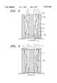
- FIG. 1Adiagrammatically illustrates a cross-section of a preferred embodiment of a miniature connector and a pin according to the current invention during an initial phase of an insertion cycle.
- FIG. 1Bdiagrammatically illustrates a top view of the miniature connector of the current invention.
- FIG. 1Cshows another cross-sectional view of the miniature connector at 1C--1C of FIG. 1B.
- FIG. 2shows a cross-sectional view of the miniature connector as in FIG. 1A and a pin during an intermediate phase of the insertion cycle.
- FIG. 3illustrates a cross-sectional view of the miniature connector and the pin of the current invention as in FIG. 1A after the pin is completely inserted into the connector.
- FIG. 4shows a top view of a further embodiment of an electrical connector in accordance with the present invention.
- FIG. 5shows a cross-sectional view taken along the lines 4--4 of the electrical connector of FIG. 4.
- FIG. 6ashows a top view of an embodiment of a connector housing in accordance with the present invention.
- FIG. 6bshows a lateral cross-sectional view taken along the lines 6b--6b of the connector housing of FIG. 6a.
- FIG. 6cshows a partial longitudinal cross-sectional view taken along the lines 6c--6c of the connector housing of FIG. 6a.
- FIG. 7ashows a receptacle and retention spring assembly in accordance with the present invention.
- FIG. 7bshows a cross-sectional view taken along the lines 7--7 of the receptacle and retention spring assembly of FIG. 7a.
- FIG. 8shows a perspective view of a pin header and connector housing in accordance with the present invention.
- FIG. 9ashows a lateral side view of a pin header in accordance with the present invention.
- FIG. 9bshows a longitudinal side view of a pin header in accordance with the present invention.
- FIG. 10shows a cross-sectional view taken along the lines 10--10 of the pin header shown in FIG. 9b.
- FIG. 11shows a cross-sectional view of another embodiment of a pin header in accordance with the present invention.
- FIGS. 12a-12eshow a row of terminal pins and alignment wafers in accordance with the present invention.
- FIGS. 13a-13dshow a stand-off pin guide in accordance with the present invention.
- FIG. 1Ashows a cross sectional view of one preferred embodiment of a compact connector assembly according to the current invention.
- the assembly 1comprises a pin 2 and a compact connector or receptacle 3.
- the compact connector 3further comprises a side wall 4, an inner wall 5 and an electrically-conductive composite action beam 6.
- the composite action beam 6is located in a bore 7 which is limited by the inner wall 5 and the sidewall 4.
- a movable or unsupported end 6A of the composite action beam 6is located near a pin receiving opening 8 while a fixed or supported end 6B of the composite action beam 6 is located near a solder tail opening 9.
- a solder tail 10 of the composite action beam 6is continuous with the composite action beam 6 at the fixed end 6B and protrudes through the solder tail opening 9.
- the solder tail 10bends 90° around a bottom of the sidewall 4 and extends horizontally beyond the sidewall 4.
- the movable end 6Amakes a contact with the pin 2 during an initial phase of an insertion cycle.
- the angle of attack by the pin 2 with respect to the movable end 6Amay be relatively high during this initial phase, compared to later phases of the insertion cycle.
- the movable side 6Ais located to one side of the pin receiving opening 8 during this phase of insertion.
- the center of arch 6C of the composite action beam 6can abut against the inside wall 5.
- the pin-receiving opening 8can be partially further indented on a surface 4A facing the movable end 6A.
- the deflection rate during the initial phasecan be approximately 4 gram per mil according to a preferred embodiment of the current invention.
- the movable end 6Afunctions as a cantilever beam and requires low insertion force during this initial phase.
- FIG. 1Brelative locations of the above discussed components in the compact connector according to the current invention are shown in a top view.
- the pin 2In a pin-receiving opening 8, the pin 2 is shown in the most inner part against the inner wall 5.
- the pin 2contacts the movable end 6A of the composite action beam 6 in an approximately center location of the pin receiving opening 8.
- Lateral to the movable end 6Ais a space 7 and the fixed end 6B which abuts the sidewall 4.
- Further lateral to the sidewall 4is a portion of the solder tail 10, which extends beyond the sidewall 4.
- there are eight pin-to-beam contacts on the connectorthere are eight pin-to-beam contacts on the connector. It is noted, however, that such a connector feature would most likely be applicable in high pin count configurations.
- FIG. 1Cshows another cross-sectional view of the miniature connector at 1C--1C of FIG. 1B.
- the pin-receiving opening 8has a larger diameter than the width of the composite action beam 6.
- the bore 7 indicated by a dotted lineis limited by the inside walls of the connector 3.
- the composite action beam 6 shown in solid linehas the movable end 6A near the pin-receiving opening 8, the arch portion 6C near the center of the bore 7 and the fixed end 6B near the solder tail opening 9.
- the solder tail 10is contiguous with the fixed end 6B.
- the indented surface 4Afurther comprises a transition area 4B between the indented surface 4A and the inner surface of the side wall 4.
- the indented surfacefurther comprises movable area 4C where a movement of the movable end 6A of the composite action beam 6 is accommodated.
- the movable end of the composite action beam 6is guided within movable area 4C of the indented surface 4A so as to minimize the deviation from a predetermined course of movement.
- the width of the movable end 6A and the corresponding moveable area 4Cis wider than the rest of the composite action beam 6 or the bore 7. This width differentiation prevents the moveable end 6A of the composite action beam from being pushed down towards the fixed end 6B so as to maintain its substantially horizontal movement near the pin-receiving opening 8 during the pin insertion cycle.
- solder tail opening 9is filled. In such a construction it may not be necessary to provide movable end 6A with a portion that is wider than the composite action beam 6 or bore 7. Similarly, if movable end 6A is constructed as shown, it may not be necessary to fill solder tail opening 9.
- One advantage to filling solder tail opening 9is the prevention of solder from flowing into bore 7 during mounting of the connector.
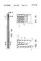
- FIG. 2illustrates an intermediate phase of the pin insertion cycle in a preferred embodiment according to the current invention as shown in FIG. 1A.
- the pinis further inserted towards the center of the arch 6C of the composite action beam 6.
- the movable end 6Afunctions as a cantilever beam, and the movable end 6A moves towards the partially indented surface 4A of the sidewall 4.
- the partially indented surface 4A of the sidewall 4can serve to narrow the overall width of the connector assembly 1.
- the movable endthen abuts against the partially intended surface 4A as shown in FIG. 2.
- the composite action beam 6goes through a transition from a cantilever beam to a supported beam.
- the center of the arch 6Cdeflects from this point on.
- the movable end 6Amay move in the direction of an axis of insertion toward the pin receiving opening 8.
- the fixed end 6B of the composite action beam 6remains stationary with respect to the sidewall 4. Accordingly, the deflection rate may increase up to approximately 16 grams per mil after the composite beam 6 acts as a two-point supported beam in a preferred embodiment of the current invention.
- the pin 2has reached the final insertion point.
- the pin 2is pressed against the inner wall 5 by the composite action beam 6 at a Hertzian stress dot 6D.
- the composite action beam 6provides high normal force against the pin 2 relative to initial insertion force so as to retain the pin 2 in the final position.
- the composite action beam 6now remains to function as a two-point supported beam.
- top 11has been added to connector i which extends over pin receiving opening 8.
- the function of top 11is to prevent stubbing of pins 2 on composite beam 6.
- the end portion of top 11 extending over pin receiving opening 8is chamfered or tapered.
- FIGS. 1-3illustrate a transition of the composite action beam 6 from a cantilever beam to a supported beam.
- Such a transition in the beam 6yields low insertion force during an initial phase relative to high normal force against a completely inserted pin.
- Low insertion forceis an advantage for a compact connector. Since the area required for each pin-to-beam contact is smaller with the composite action beam of the current invention, a larger number of the contacts may be placed in the compact connector. Thus, a total amount of insertion force needs to be kept minimal so as to make insertion relatively easy and reliable.
- the composite action beam of the current inventionsatisfies such a low insertion force requirement.
- the composite action beam of the current inventioncombines the advantageous features of the cantilever beam and the supported beam without sacrificing the space limitation of a compact connector.
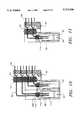
- FIGS. 4 and 5Another embodiment of an electrical connector in accordance with the present invention is shown in FIGS. 4 and 5.
- adjacent pin insertion openings 20 in the connector housing 22are closely spaced together, both in the longitudinal and lateral direction.
- a counter-sink bore 24 of each pin insertion opening 20is in communication with an insertion bore 26 such that the counter-sink bore facilitates easy insertion of adjacent pins 28 into the insertion bores 26 of laterally adjacent pin insertion openings 20.
- Pin 28 and the counter-sink bore 24 and insertion bore 26all have a coincidental central axis 30 such that the pins 28 are inserted into the openings 20 along the central axis 30.
- the insertion bores 26are only slightly larger than, and preferably the same shape as, the external surface of the pins 28, taking into account the necessary tolerances of the structure.
- each opening 20is in communication with a spring retention bore 32 in the housing, with the central axis of the spring retention bore being parallel to, but displaced from, the axis of insertion of the pins along central axis 30.
- a surface 34 of the insertion bore 26is substantially aligned with a surface 36 of the spring retention bore 32 such that the pins 28 are inserted into the spring retention bore closely adjacent to, and preferably contacting, the surface 36 of the spring retention bore 32.
- the pins 28are thus inserted into contact with the contact beams 38 in the manner described above such that the pins are retained against the surface 36. In this manner, the tolerances of the assembly can be low, while ensuring that the pins contact a wall of the housing when the contact beam applies a high normal force in order to retain the pins in the housing.
- the connector housing 22has a cavity 40 in the bottom surface 41.
- the contact beams 38are mounted in a receptacle 42 such that the contact beams are detachably mounted within the housing when the receptacle 42 is mounted into the cavity 40.
- one row of contact beamsis disposed in one half of a receptacle 42.
- each half of the receptacle 42includes alternating pins 44 and holes 46, which are preferably square.
- these rows of contact beamsare easily manufactured separately and subsequently assembled together with the pins of one row connected into a corresponding hole of another row in a known manner to form a single receptacle having adjacent rows of contact beams. Accordingly, the rows of adjacent contact beams are inserted into the spring retention bore and detentes 48 on the receptacle 42 engage the walls 50 of the connector housing, causing elastic deformation of the walls in the area of the detentes, such that the receptacle is mechanically connected to the connector housing.
- connector housing 22in order to facilitate insertion of the contact beam rows into the housing, in a preferred embodiment connector housing 22 includes beam insertion ramps 52. These ramps comprise a flat portion 54, extending from the base of the insertion bore, and a sloped portion 56 which extends toward the bottom surface 41 of the connector housing. Upon insertion of the contact beams in the spring retention bore, the contact beams slide up the sloped portion 54 and onto the flat portion 56 such that all of the insertion tolerances are applied to one side of the connector housing and can be accounted for during manufacture of the connector structure.
- a preferred embodiment of a contact beam 38is shown in FIG. 7b.
- a straight portion 60is disposed within the receptacle 42.
- the straight portion 60is molded into the receptacle during the manufacture of the beam and receptacle assembly such that solder used to mount the contact beam to a printed substrate cannot flow from the bottom of the connector housing and into the spring retention bore.
- Another straight portion 62extends at an angle from one end of the straight portion 60.
- the straight portion 62is joined to a curved contact portion 64 and the curved contact portion 64 is joined to top portion 66.
- the end of the contact beam including the straight portion 60 and curved contact portion 64is the end that is inserted into the spring retention bore, as shown in FIG. 5.
- the pins 28when the pins 28 are inserted into the openings 20 of the housing 22 they contact the curved contact portion 64 of the contact beam 38 and the top portion 66 of the beam deflects away from the surface 36.
- the curved contact portion of the contact beamapplies a high normal force against the pins for retaining the pins in the housing in the manner described above.
- mounting portion 68 of the contact beamextends from the other end of straight portion 60.
- mounting portion 68is for straddle mounting of the connector wherein the mounting portion of the contact beam in the adjacent rows of beams is soldered to a pad on either side of a printed circuit board or the like in a known manner.
- the present inventionis not intended to be limited in this manner and a known mounting portion for surface mounting the connector is within the scope of the invention.
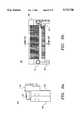
- a terminal pin header 80 for mating with connector housing 22is shown in FIG. 8.
- Electrical connectionis established between a plurality of terminal pins 82 disposed in the header 80 and the contact beams 38 disposed in connector housing 22.
- Header 80is a right angle header wherein the terminal pins 82 are bent substantially at right angles within the header in the manner set forth in further detail below.
- the circuit board end 84 of the terminal pinsis inserted into holes 85 in a printed circuit board 86 and solderably connected thereto in a known manner for establishing electrical connection between the printed circuitry (not shown) on the circuit board and the contact beams 38. Accordingly, the mounting portion 68 of the contact beams 38 can be connected to a second printed circuit board or the like such that an electrical connection is established between the first and second printed circuit boards for carrying out a variety of functions in a known manner.
- the terminal pins 82are disposed in header housing 88 and stand-off pin guide 90, wherein pin guide 90 is bolted to header housing 88 by bolts 91.
- pin guide 90is bolted to header housing 88 by bolts 91.
- FIGS. 9a and 10in one embodiment of the present invention eight longitudinal rows of terminal pins 82 are disposed in the pin header 80. In this embodiment, two adjacent header housings 88 are mated together.
- the present inventionis not intended to be limited in this manner, and any number of longitudinal rows of pins can be provided, depending upon the application requirements.
- four longitudinal rows of terminal pinsare provided with only one header housing 88.
- the pinsare aligned in two adjacent rows per each header housing 88.
- at least two of the pins extending out of the first surfacehave equal lengths.
- the first end of the terminal pinhas at least two terminals of substantially equal lengths and the second end of the terminals pin has a single terminal.
- the number and arrangement of the terminal pin rows at the circuit board end 84 of the pins 82can be configured to meet the desired mating requirements for the printed circuit board.
- the pinsare bent substantially at a right angle 93 with the pins in one vertical column being bent in an upward direction and the pins in an adjacent vertical column being bent in a downward direction.
- the connector housingis inserted into the cavity 94 in the header housing 88.
- two separate connector housings 22are mated with the header.
- the connector end 92 of the two adjacent rows of terminal pinsis inserted into the corresponding adjacent rows of pin insertion openings 20 such that the pins contact the contact beams 38 in the manner described above.
- the pinsare simply inserted into the connector housing 22 without interference such as pin stubbing.
- a longitudinal row 98 of terminal pins 82is molded into a top retention and alignment wafer 100 and a bottom retention and alignment wafer 102, the wafers 100 and 102 comprising a molded plastic material.
- the terminal pinsare aligned in a die and the molded wafers are formed out of molten plastic material with projections 104 and sockets 106 being formed as part of the wafers.
- projections in the moldform the sockets 106. The projections on the mold extend into contact with and positively locate the row of pins, i.e.
- sockets 106extend into contact with the pins, such that alignment of the pins can be measured and maintained within a desired tolerance.
- the pinscan be embossed to form a bulge 107 such that the bulge is used to positively secure the row of pins in the header housing when the pins are inserted therein in the manner set forth below.
- adjacent rows of pinsare properly aligned within the header housing such that the desired tolerances of the connector components are maintained and the header can be simply mated with the connector housing such that the pins are effectively connected to the contact beams in the connector housing in the manner set forth above.
- stand-off pin guide 90in order to provide for proper alignment, within a desired tolerance, of the circuit board end 84 of the pins when the pins are connected to the printed circuit board 86, stand-off pin guide 90 includes a plurality of longitudinal rows of pin guide holes 120. In the embodiment shown in FIG. 13a, eight longitudinal rows of pin guide holes are provided for receiving eight rows of terminal pins discussed above. It should be noted that the rear surface 122 of the pin guide is mounted to the header housing 88 with the bolts 91 extending through bolt holes 123.
- ridges in the pin guideform four inclined ramp surfaces 124, 125, 126, 127 around each of the holes 120 wherein the ramp surfaces extend into communication with the holes 120. Accordingly, the pins are positively inserted into the pin guide 90 along the ramp surfaces and into the holes 120. Thus, pin stubbing is obviated and the ridges ensure that the pins are properly guided into the pin guide holes.
- the present inventionprovides for connection of a large array of pins to a printed circuit board such that all of the pins are properly aligned and thus, can be simply inserted into their respective holes on the board.
Landscapes
- Coupling Device And Connection With Printed Circuit (AREA)
Abstract
Description
Claims (3)
Priority Applications (1)
| Application Number | Priority Date | Filing Date | Title |
|---|---|---|---|
| US08/643,072US5713746A (en) | 1994-02-08 | 1996-04-30 | Electrical connector |
Applications Claiming Priority (4)
| Application Number | Priority Date | Filing Date | Title |
|---|---|---|---|
| US19344394A | 1994-02-08 | 1994-02-08 | |
| US22107794A | 1994-03-31 | 1994-03-31 | |
| US08/235,289US5511984A (en) | 1994-02-08 | 1994-04-29 | Electrical connector |
| US08/643,072US5713746A (en) | 1994-02-08 | 1996-04-30 | Electrical connector |
Related Parent Applications (1)
| Application Number | Title | Priority Date | Filing Date |
|---|---|---|---|
| US08/235,289ContinuationUS5511984A (en) | 1994-02-08 | 1994-04-29 | Electrical connector |
Publications (1)
| Publication Number | Publication Date |
|---|---|
| US5713746Atrue US5713746A (en) | 1998-02-03 |
Family
ID=27393198
Family Applications (1)
| Application Number | Title | Priority Date | Filing Date |
|---|---|---|---|
| US08/643,072Expired - LifetimeUS5713746A (en) | 1994-02-08 | 1996-04-30 | Electrical connector |
Country Status (6)
| Country | Link |
|---|---|
| US (1) | US5713746A (en) |
| EP (1) | EP0801821B1 (en) |
| JP (1) | JPH09508749A (en) |
| DE (1) | DE69531165T2 (en) |
| SG (2) | SG50495A1 (en) |
| WO (1) | WO1995022182A1 (en) |
Cited By (50)
| Publication number | Priority date | Publication date | Assignee | Title |
|---|---|---|---|---|
| US5980272A (en)* | 1997-10-21 | 1999-11-09 | Hon Hai Precision Ind. Co., Ltd. | Electrical connector with back shell for contact tails |
| US6093032A (en)* | 1997-10-22 | 2000-07-25 | Mchugh; Robert G. | Connector with spacer |
| USD432501S (en) | 1999-10-05 | 2000-10-24 | Honda Tsushin Kogyo Co., Ltd. | Electric connector receptacle |
| US6267623B1 (en)* | 1997-10-03 | 2001-07-31 | Japan Aviation Electronics Industry, Limited | Electrical connector with a mating portion defined by a metallic shell |
| US6325646B1 (en)* | 1999-11-17 | 2001-12-04 | Nintendo Co., Ltd. | Power plug assembly having a plug that is lifted up when plugged into an outlet |
| US20040116000A1 (en)* | 2002-12-13 | 2004-06-17 | Sandoval Alisa C | Cable connector riser |
| US20040161954A1 (en)* | 2001-07-31 | 2004-08-19 | Fci Americas Technology Inc. | Modular mezzanine connector |
| US6821161B1 (en)* | 2003-05-23 | 2004-11-23 | Hon Hai Precision Ind. Co., Ltd. | Electrical connector with protective spacer |
| US6837720B2 (en) | 2001-11-27 | 2005-01-04 | Sun Microsystems, Inc. | Connector for electrically coupling one or more devices in a processor-based system |
| US20050020136A1 (en)* | 2003-07-23 | 2005-01-27 | Johannes Richard A. | Electrical connector contact |
| US20050170700A1 (en)* | 2001-11-14 | 2005-08-04 | Shuey Joseph B. | High speed electrical connector without ground contacts |
| US20050196987A1 (en)* | 2001-11-14 | 2005-09-08 | Shuey Joseph B. | High density, low noise, high speed mezzanine connector |
| US20050287850A1 (en)* | 2001-11-14 | 2005-12-29 | Minich Steven E | Electrical connectors having differential signal pairs configured to reduce cross-talk on adjacent pairs |
| US20050287849A1 (en)* | 2001-11-14 | 2005-12-29 | Fci Americas Technology, Inc. | Cross talk reduction and impedance matching for high speed electrical connectors |
| US20060019517A1 (en)* | 2001-11-14 | 2006-01-26 | Fci Americas Technology, Inc. | Impedance control in electrical connectors |
| US20060035530A1 (en)* | 2001-11-14 | 2006-02-16 | Fci Americas Technology, Inc. | High speed differential transmission structures without grounds |
| US20060068641A1 (en)* | 2003-09-26 | 2006-03-30 | Hull Gregory A | Impedance mathing interface for electrical connectors |
| US20060228912A1 (en)* | 2005-04-07 | 2006-10-12 | Fci Americas Technology, Inc. | Orthogonal backplane connector |
| US20060245137A1 (en)* | 2005-04-29 | 2006-11-02 | Fci Americas Technology, Inc. | Backplane connectors |
| US20070296066A1 (en)* | 2006-06-27 | 2007-12-27 | Joseph Blair Shuey | Electrical connector with elongated ground contacts |
| US20080003880A1 (en)* | 2004-09-29 | 2008-01-03 | Fci Americas Technology, Inc. | High speed connectors that minimize signal skew and crosstalk |
| US20080026632A1 (en)* | 2006-07-31 | 2008-01-31 | Eichorn Daniel S | Top mount right angle header |
| US20080045079A1 (en)* | 2006-08-21 | 2008-02-21 | Minich Steven E | Electrical Connector System With Jogged Contact Tails |
| US20080085637A1 (en)* | 2006-10-09 | 2008-04-10 | Hon Hai Precision Ind. Co., Ltd. | Electrical connector with improved housing |
| US7497736B2 (en) | 2006-12-19 | 2009-03-03 | Fci Americas Technology, Inc. | Shieldless, high-speed, low-cross-talk electrical connector |
| US7517250B2 (en) | 2003-09-26 | 2009-04-14 | Fci Americas Technology, Inc. | Impedance mating interface for electrical connectors |
| US20090221165A1 (en)* | 2008-02-29 | 2009-09-03 | Buck Jonathan E | Cross talk reduction for high speed electrical connectors |
| US7708569B2 (en) | 2006-10-30 | 2010-05-04 | Fci Americas Technology, Inc. | Broadside-coupled signal pair configurations for electrical connectors |
| US7713088B2 (en) | 2006-10-05 | 2010-05-11 | Fci | Broadside-coupled signal pair configurations for electrical connectors |
| US20100273354A1 (en)* | 2007-07-13 | 2010-10-28 | Stoner Stuart C | Electrical connector system having a continuous ground at the mating interface thereof |
| US20110021083A1 (en)* | 2009-07-24 | 2011-01-27 | Fci Americas Technology, Inc. | Dual Impedance Electrical Connector |
| US20110097934A1 (en)* | 2009-10-28 | 2011-04-28 | Minich Steven E | Electrical connector having ground plates and ground coupling bar |
| US20110117781A1 (en)* | 2009-11-13 | 2011-05-19 | Stoner Stuart C | Attachment system for electrical connector |
| US20110159744A1 (en)* | 2009-12-30 | 2011-06-30 | Buck Jonathan E | Electrical connector having impedance tuning ribs |
| US8540525B2 (en) | 2008-12-12 | 2013-09-24 | Molex Incorporated | Resonance modifying connector |
| US8545240B2 (en) | 2008-11-14 | 2013-10-01 | Molex Incorporated | Connector with terminals forming differential pairs |
| USD718253S1 (en) | 2012-04-13 | 2014-11-25 | Fci Americas Technology Llc | Electrical cable connector |
| US8905651B2 (en) | 2012-01-31 | 2014-12-09 | Fci | Dismountable optical coupling device |
| USD720698S1 (en) | 2013-03-15 | 2015-01-06 | Fci Americas Technology Llc | Electrical cable connector |
| US8944831B2 (en) | 2012-04-13 | 2015-02-03 | Fci Americas Technology Llc | Electrical connector having ribbed ground plate with engagement members |
| USD727268S1 (en) | 2012-04-13 | 2015-04-21 | Fci Americas Technology Llc | Vertical electrical connector |
| USD727852S1 (en) | 2012-04-13 | 2015-04-28 | Fci Americas Technology Llc | Ground shield for a right angle electrical connector |
| US9048583B2 (en) | 2009-03-19 | 2015-06-02 | Fci Americas Technology Llc | Electrical connector having ribbed ground plate |
| USD733662S1 (en) | 2013-01-25 | 2015-07-07 | Fci Americas Technology Llc | Connector housing for electrical connector |
| US9136634B2 (en) | 2010-09-03 | 2015-09-15 | Fci Americas Technology Llc | Low-cross-talk electrical connector |
| USD746236S1 (en) | 2012-07-11 | 2015-12-29 | Fci Americas Technology Llc | Electrical connector housing |
| US9257778B2 (en) | 2012-04-13 | 2016-02-09 | Fci Americas Technology | High speed electrical connector |
| US9277649B2 (en) | 2009-02-26 | 2016-03-01 | Fci Americas Technology Llc | Cross talk reduction for high-speed electrical connectors |
| US9543703B2 (en) | 2012-07-11 | 2017-01-10 | Fci Americas Technology Llc | Electrical connector with reduced stack height |
| US10243284B2 (en) | 2011-01-31 | 2019-03-26 | Amphenol Corporation | Multi-stage beam contacts |
Families Citing this family (5)
| Publication number | Priority date | Publication date | Assignee | Title |
|---|---|---|---|---|
| DE102004027712B4 (en)* | 2004-06-07 | 2007-09-06 | Tyco Electronics Amp Gmbh | Contact arrangement for circuit boards |
| US8512081B2 (en)* | 2011-01-31 | 2013-08-20 | Amphenol Corporation | Multi-stage beam contacts |
| KR101314105B1 (en)* | 2011-10-12 | 2013-10-04 | 주식회사 유라코퍼레이션 | Auto transmission harness |
| CN104347988B (en)* | 2013-08-02 | 2018-09-25 | 安费诺公司 | Multistage beam type contact |
| WO2024195294A1 (en)* | 2023-03-20 | 2024-09-26 | 株式会社村田製作所 | Connector and connector set |
Citations (16)
| Publication number | Priority date | Publication date | Assignee | Title |
|---|---|---|---|---|
| GB879968A (en)* | 1958-01-20 | 1961-10-11 | Siemens Ag | Improvements relating to electrical plug and socket connectors |
| US3963317A (en)* | 1975-04-03 | 1976-06-15 | E. I. Du Pont De Nemours And Company | Zero force edge connector block |
| US4036544A (en)* | 1974-10-16 | 1977-07-19 | Bunker Ramo Corporation | Contact for multiple conductor connector |
| US4420215A (en)* | 1979-12-26 | 1983-12-13 | A P Products Incorporated | Variable effective length cantilever contact and connector |
| US4775333A (en)* | 1985-12-23 | 1988-10-04 | Ford Motor Company | Method of assembling an improved electrical connector |
| US4846734A (en)* | 1988-01-22 | 1989-07-11 | Burndy Corporation | Vertical edge card connectors |
| US4871320A (en)* | 1987-10-16 | 1989-10-03 | E. I. Du Pont De Nemours And Company | Pin holder |
| US5066236A (en)* | 1989-10-10 | 1991-11-19 | Amp Incorporated | Impedance matched backplane connector |
| US5074039A (en)* | 1990-10-26 | 1991-12-24 | Amp Incorporated | Method of manufacturing electrical connectors |
| US5133679A (en)* | 1990-06-08 | 1992-07-28 | E. I. Du Pont De Nemours And Company | Connectors with ground structure |
| US5197893A (en)* | 1990-03-14 | 1993-03-30 | Burndy Corporation | Connector assembly for printed circuit boards |
| US5213514A (en)* | 1990-09-17 | 1993-05-25 | Hirose Electric Co., Ltd. | Multipole electrical connector |
| US5236368A (en)* | 1992-01-06 | 1993-08-17 | Burndy Corporation | Printed circuit board and outrigger edge connector assembly and method of assembling the same |
| US5273461A (en)* | 1992-08-28 | 1993-12-28 | Lee Chih Ta | Electronic connector for electrically connecting an electronic module to a printed circuit board |
| US5387114A (en)* | 1993-07-22 | 1995-02-07 | Molex Incorporated | Electrical connector with means for altering circuit characteristics |
| US5413491A (en)* | 1993-10-13 | 1995-05-09 | Burndy Corporation | Small form factor connectors with center ground plate |
Family Cites Families (1)
| Publication number | Priority date | Publication date | Assignee | Title |
|---|---|---|---|---|
| JP2570939Y2 (en)* | 1992-03-26 | 1998-05-13 | 日本エー・エム・ピー株式会社 | Shielded electrical connector and fixing bracket used for it |
- 1995
- 1995-02-06WOPCT/US1995/001465patent/WO1995022182A1/enactiveIP Right Grant
- 1995-02-06DEDE69531165Tpatent/DE69531165T2/ennot_activeExpired - Lifetime
- 1995-02-06EPEP95910176Apatent/EP0801821B1/ennot_activeExpired - Lifetime
- 1995-02-06JPJP7521274Apatent/JPH09508749A/enactivePending
- 1995-02-06SGSG1996002802Apatent/SG50495A1/enunknown
- 1995-02-06SGSG9903980Apatent/SG85669A1/enunknown
- 1996
- 1996-04-30USUS08/643,072patent/US5713746A/ennot_activeExpired - Lifetime
Patent Citations (16)
| Publication number | Priority date | Publication date | Assignee | Title |
|---|---|---|---|---|
| GB879968A (en)* | 1958-01-20 | 1961-10-11 | Siemens Ag | Improvements relating to electrical plug and socket connectors |
| US4036544A (en)* | 1974-10-16 | 1977-07-19 | Bunker Ramo Corporation | Contact for multiple conductor connector |
| US3963317A (en)* | 1975-04-03 | 1976-06-15 | E. I. Du Pont De Nemours And Company | Zero force edge connector block |
| US4420215A (en)* | 1979-12-26 | 1983-12-13 | A P Products Incorporated | Variable effective length cantilever contact and connector |
| US4775333A (en)* | 1985-12-23 | 1988-10-04 | Ford Motor Company | Method of assembling an improved electrical connector |
| US4871320A (en)* | 1987-10-16 | 1989-10-03 | E. I. Du Pont De Nemours And Company | Pin holder |
| US4846734A (en)* | 1988-01-22 | 1989-07-11 | Burndy Corporation | Vertical edge card connectors |
| US5066236A (en)* | 1989-10-10 | 1991-11-19 | Amp Incorporated | Impedance matched backplane connector |
| US5197893A (en)* | 1990-03-14 | 1993-03-30 | Burndy Corporation | Connector assembly for printed circuit boards |
| US5133679A (en)* | 1990-06-08 | 1992-07-28 | E. I. Du Pont De Nemours And Company | Connectors with ground structure |
| US5213514A (en)* | 1990-09-17 | 1993-05-25 | Hirose Electric Co., Ltd. | Multipole electrical connector |
| US5074039A (en)* | 1990-10-26 | 1991-12-24 | Amp Incorporated | Method of manufacturing electrical connectors |
| US5236368A (en)* | 1992-01-06 | 1993-08-17 | Burndy Corporation | Printed circuit board and outrigger edge connector assembly and method of assembling the same |
| US5273461A (en)* | 1992-08-28 | 1993-12-28 | Lee Chih Ta | Electronic connector for electrically connecting an electronic module to a printed circuit board |
| US5387114A (en)* | 1993-07-22 | 1995-02-07 | Molex Incorporated | Electrical connector with means for altering circuit characteristics |
| US5413491A (en)* | 1993-10-13 | 1995-05-09 | Burndy Corporation | Small form factor connectors with center ground plate |
Non-Patent Citations (1)
| Title |
|---|
| Berg Electronics Product Catalog, 3 pages.* |
Cited By (120)
| Publication number | Priority date | Publication date | Assignee | Title |
|---|---|---|---|---|
| US6267623B1 (en)* | 1997-10-03 | 2001-07-31 | Japan Aviation Electronics Industry, Limited | Electrical connector with a mating portion defined by a metallic shell |
| US5980272A (en)* | 1997-10-21 | 1999-11-09 | Hon Hai Precision Ind. Co., Ltd. | Electrical connector with back shell for contact tails |
| US6093032A (en)* | 1997-10-22 | 2000-07-25 | Mchugh; Robert G. | Connector with spacer |
| USD432501S (en) | 1999-10-05 | 2000-10-24 | Honda Tsushin Kogyo Co., Ltd. | Electric connector receptacle |
| US6325646B1 (en)* | 1999-11-17 | 2001-12-04 | Nintendo Co., Ltd. | Power plug assembly having a plug that is lifted up when plugged into an outlet |
| US7429176B2 (en) | 2001-07-31 | 2008-09-30 | Fci Americas Technology, Inc. | Modular mezzanine connector |
| US20040161954A1 (en)* | 2001-07-31 | 2004-08-19 | Fci Americas Technology Inc. | Modular mezzanine connector |
| US7229318B2 (en) | 2001-11-14 | 2007-06-12 | Fci Americas Technology, Inc. | Shieldless, high-speed electrical connectors |
| US20070190825A1 (en)* | 2001-11-14 | 2007-08-16 | Fci Americas Technology, Inc. | High-density, low-noise, high-speed mezzanine connector |
| US7390218B2 (en) | 2001-11-14 | 2008-06-24 | Fci Americas Technology, Inc. | Shieldless, high-speed electrical connectors |
| US20080214029A1 (en)* | 2001-11-14 | 2008-09-04 | Lemke Timothy A | Shieldless, High-Speed Electrical Connectors |
| US7331800B2 (en) | 2001-11-14 | 2008-02-19 | Fci Americas Technology, Inc. | Shieldless, high-speed electrical connectors |
| US20050170700A1 (en)* | 2001-11-14 | 2005-08-04 | Shuey Joseph B. | High speed electrical connector without ground contacts |
| US20050196987A1 (en)* | 2001-11-14 | 2005-09-08 | Shuey Joseph B. | High density, low noise, high speed mezzanine connector |
| US20050287850A1 (en)* | 2001-11-14 | 2005-12-29 | Minich Steven E | Electrical connectors having differential signal pairs configured to reduce cross-talk on adjacent pairs |
| US20050287849A1 (en)* | 2001-11-14 | 2005-12-29 | Fci Americas Technology, Inc. | Cross talk reduction and impedance matching for high speed electrical connectors |
| US20060019517A1 (en)* | 2001-11-14 | 2006-01-26 | Fci Americas Technology, Inc. | Impedance control in electrical connectors |
| US20080248693A1 (en)* | 2001-11-14 | 2008-10-09 | Fci Americas Technology, Inc. | Shieldless, high-speed electrical connectors |
| US7442054B2 (en) | 2001-11-14 | 2008-10-28 | Fci Americas Technology, Inc. | Electrical connectors having differential signal pairs configured to reduce cross-talk on adjacent pairs |
| US20060035530A1 (en)* | 2001-11-14 | 2006-02-16 | Fci Americas Technology, Inc. | High speed differential transmission structures without grounds |
| US20060063404A1 (en)* | 2001-11-14 | 2006-03-23 | Fci Americas Technology, Inc. | Electrical connectors having contacts that may be selectively designated as either signal or ground contacts |
| US7467955B2 (en) | 2001-11-14 | 2008-12-23 | Fci Americas Technology, Inc. | Impedance control in electrical connectors |
| US7114964B2 (en) | 2001-11-14 | 2006-10-03 | Fci Americas Technology, Inc. | Cross talk reduction and impedance matching for high speed electrical connectors |
| US7118391B2 (en) | 2001-11-14 | 2006-10-10 | Fci Americas Technology, Inc. | Electrical connectors having contacts that may be selectively designated as either signal or ground contacts |
| US7309239B2 (en) | 2001-11-14 | 2007-12-18 | Fci Americas Technology, Inc. | High-density, low-noise, high-speed mezzanine connector |
| US7390200B2 (en) | 2001-11-14 | 2008-06-24 | Fci Americas Technology, Inc. | High speed differential transmission structures without grounds |
| US20060234532A1 (en)* | 2001-11-14 | 2006-10-19 | Fci Americas Technology, Inc. | Shieldless, high-speed electrical connectors |
| US20060246756A1 (en)* | 2001-11-14 | 2006-11-02 | Fci Americas Technology, Inc. | Shieldless, high-speed electrical connectors |
| US20070099464A1 (en)* | 2001-11-14 | 2007-05-03 | Winings Clifford L | Shieldless, High-Speed Electrical Connectors |
| US20070059952A1 (en)* | 2001-11-14 | 2007-03-15 | Fci Americas Technology, Inc. | Impedance control in electrical connectors |
| US7182643B2 (en) | 2001-11-14 | 2007-02-27 | Fci Americas Technology, Inc. | Shieldless, high-speed electrical connectors |
| US6837720B2 (en) | 2001-11-27 | 2005-01-04 | Sun Microsystems, Inc. | Connector for electrically coupling one or more devices in a processor-based system |
| US6793507B2 (en)* | 2002-12-13 | 2004-09-21 | Hewlett-Packard Development Company, L.P. | Cable connector riser |
| US20040116000A1 (en)* | 2002-12-13 | 2004-06-17 | Sandoval Alisa C | Cable connector riser |
| US6821161B1 (en)* | 2003-05-23 | 2004-11-23 | Hon Hai Precision Ind. Co., Ltd. | Electrical connector with protective spacer |
| US20040235361A1 (en)* | 2003-05-23 | 2004-11-25 | Xiang Cao | Electrical connector with protective spacer |
| US20070015397A1 (en)* | 2003-07-23 | 2007-01-18 | Fci Americas Technology, Inc. | Electrical connector contact |
| US7303441B2 (en) | 2003-07-23 | 2007-12-04 | Fci Americas Technology, Inc. | Electrical connector contact |
| US7241175B2 (en) | 2003-07-23 | 2007-07-10 | Fci Americas Technology, Inc. | Electrical connector contact |
| US7547232B2 (en) | 2003-07-23 | 2009-06-16 | Fci Americas Technology, Inc. | Electrical connector contact |
| US20060035524A1 (en)* | 2003-07-23 | 2006-02-16 | Fci Americas Technology, Inc. | Electrical connector contact |
| US6997750B2 (en) | 2003-07-23 | 2006-02-14 | Fci Americas Technology, Inc. | Electrical connector contact |
| US7121892B2 (en) | 2003-07-23 | 2006-10-17 | Fci Americas Technology, Inc. | Electrical connector contact |
| US20050020136A1 (en)* | 2003-07-23 | 2005-01-27 | Johannes Richard A. | Electrical connector contact |
| US7491100B2 (en) | 2003-07-23 | 2009-02-17 | Fci Americas Technology, Inc. | Electrical connector contact |
| US20080057790A1 (en)* | 2003-07-23 | 2008-03-06 | Fci Americas Technology, Inc. | Electrical connector contact |
| US20080171471A1 (en)* | 2003-07-23 | 2008-07-17 | Fci Americas Technology, Inc. | Electrical connector contact |
| US7524209B2 (en) | 2003-09-26 | 2009-04-28 | Fci Americas Technology, Inc. | Impedance mating interface for electrical connectors |
| US7837504B2 (en) | 2003-09-26 | 2010-11-23 | Fci Americas Technology, Inc. | Impedance mating interface for electrical connectors |
| US20060068641A1 (en)* | 2003-09-26 | 2006-03-30 | Hull Gregory A | Impedance mathing interface for electrical connectors |
| US7517250B2 (en) | 2003-09-26 | 2009-04-14 | Fci Americas Technology, Inc. | Impedance mating interface for electrical connectors |
| US7497735B2 (en) | 2004-09-29 | 2009-03-03 | Fci Americas Technology, Inc. | High speed connectors that minimize signal skew and crosstalk |
| US20080003880A1 (en)* | 2004-09-29 | 2008-01-03 | Fci Americas Technology, Inc. | High speed connectors that minimize signal skew and crosstalk |
| US20060228912A1 (en)* | 2005-04-07 | 2006-10-12 | Fci Americas Technology, Inc. | Orthogonal backplane connector |
| US20060245137A1 (en)* | 2005-04-29 | 2006-11-02 | Fci Americas Technology, Inc. | Backplane connectors |
| US20090149041A1 (en)* | 2006-03-24 | 2009-06-11 | Morlion Danny L C | Orthogonal Backplane Connector |
| US7462924B2 (en) | 2006-06-27 | 2008-12-09 | Fci Americas Technology, Inc. | Electrical connector with elongated ground contacts |
| US20070296066A1 (en)* | 2006-06-27 | 2007-12-27 | Joseph Blair Shuey | Electrical connector with elongated ground contacts |
| US20080026632A1 (en)* | 2006-07-31 | 2008-01-31 | Eichorn Daniel S | Top mount right angle header |
| US7331801B1 (en) | 2006-07-31 | 2008-02-19 | Delphi Technologies, Inc. | Top mount right angle header |
| US7500871B2 (en) | 2006-08-21 | 2009-03-10 | Fci Americas Technology, Inc. | Electrical connector system with jogged contact tails |
| US20090124101A1 (en)* | 2006-08-21 | 2009-05-14 | Minich Steven E | Electrical connector system with jogged contact tails |
| US7837505B2 (en) | 2006-08-21 | 2010-11-23 | Fci Americas Technology Llc | Electrical connector system with jogged contact tails |
| US20080045079A1 (en)* | 2006-08-21 | 2008-02-21 | Minich Steven E | Electrical Connector System With Jogged Contact Tails |
| US7713088B2 (en) | 2006-10-05 | 2010-05-11 | Fci | Broadside-coupled signal pair configurations for electrical connectors |
| US7534150B2 (en)* | 2006-10-09 | 2009-05-19 | Hon Hai Precision Ind. Co., Ltd. | Electrical connector with improved housing |
| US20080085637A1 (en)* | 2006-10-09 | 2008-04-10 | Hon Hai Precision Ind. Co., Ltd. | Electrical connector with improved housing |
| US7708569B2 (en) | 2006-10-30 | 2010-05-04 | Fci Americas Technology, Inc. | Broadside-coupled signal pair configurations for electrical connectors |
| US8096832B2 (en) | 2006-12-19 | 2012-01-17 | Fci Americas Technology Llc | Shieldless, high-speed, low-cross-talk electrical connector |
| US20100291806A1 (en)* | 2006-12-19 | 2010-11-18 | Minich Steven E | Shieldless, High-Speed, Low-Cross-Talk Electrical Connector |
| US8678860B2 (en) | 2006-12-19 | 2014-03-25 | Fci Americas Technology Llc | Shieldless, high-speed, low-cross-talk electrical connector |
| US7762843B2 (en) | 2006-12-19 | 2010-07-27 | Fci Americas Technology, Inc. | Shieldless, high-speed, low-cross-talk electrical connector |
| US7497736B2 (en) | 2006-12-19 | 2009-03-03 | Fci Americas Technology, Inc. | Shieldless, high-speed, low-cross-talk electrical connector |
| US8382521B2 (en) | 2006-12-19 | 2013-02-26 | Fci Americas Technology Llc | Shieldless, high-speed, low-cross-talk electrical connector |
| US20100273354A1 (en)* | 2007-07-13 | 2010-10-28 | Stoner Stuart C | Electrical connector system having a continuous ground at the mating interface thereof |
| US8137119B2 (en) | 2007-07-13 | 2012-03-20 | Fci Americas Technology Llc | Electrical connector system having a continuous ground at the mating interface thereof |
| US20090221165A1 (en)* | 2008-02-29 | 2009-09-03 | Buck Jonathan E | Cross talk reduction for high speed electrical connectors |
| US8764464B2 (en) | 2008-02-29 | 2014-07-01 | Fci Americas Technology Llc | Cross talk reduction for high speed electrical connectors |
| US8545240B2 (en) | 2008-11-14 | 2013-10-01 | Molex Incorporated | Connector with terminals forming differential pairs |
| US8540525B2 (en) | 2008-12-12 | 2013-09-24 | Molex Incorporated | Resonance modifying connector |
| US8992237B2 (en) | 2008-12-12 | 2015-03-31 | Molex Incorporated | Resonance modifying connector |
| US8651881B2 (en) | 2008-12-12 | 2014-02-18 | Molex Incorporated | Resonance modifying connector |
| US9277649B2 (en) | 2009-02-26 | 2016-03-01 | Fci Americas Technology Llc | Cross talk reduction for high-speed electrical connectors |
| US9461410B2 (en) | 2009-03-19 | 2016-10-04 | Fci Americas Technology Llc | Electrical connector having ribbed ground plate |
| US9048583B2 (en) | 2009-03-19 | 2015-06-02 | Fci Americas Technology Llc | Electrical connector having ribbed ground plate |
| US10096921B2 (en) | 2009-03-19 | 2018-10-09 | Fci Usa Llc | Electrical connector having ribbed ground plate |
| US10720721B2 (en) | 2009-03-19 | 2020-07-21 | Fci Usa Llc | Electrical connector having ribbed ground plate |
| US8608510B2 (en) | 2009-07-24 | 2013-12-17 | Fci Americas Technology Llc | Dual impedance electrical connector |
| US20110021083A1 (en)* | 2009-07-24 | 2011-01-27 | Fci Americas Technology, Inc. | Dual Impedance Electrical Connector |
| US20110097934A1 (en)* | 2009-10-28 | 2011-04-28 | Minich Steven E | Electrical connector having ground plates and ground coupling bar |
| US8267721B2 (en) | 2009-10-28 | 2012-09-18 | Fci Americas Technology Llc | Electrical connector having ground plates and ground coupling bar |
| US8616919B2 (en) | 2009-11-13 | 2013-12-31 | Fci Americas Technology Llc | Attachment system for electrical connector |
| US20110117781A1 (en)* | 2009-11-13 | 2011-05-19 | Stoner Stuart C | Attachment system for electrical connector |
| US8715003B2 (en) | 2009-12-30 | 2014-05-06 | Fci Americas Technology Llc | Electrical connector having impedance tuning ribs |
| US20110159744A1 (en)* | 2009-12-30 | 2011-06-30 | Buck Jonathan E | Electrical connector having impedance tuning ribs |
| US9136634B2 (en) | 2010-09-03 | 2015-09-15 | Fci Americas Technology Llc | Low-cross-talk electrical connector |
| US11201418B2 (en) | 2011-01-31 | 2021-12-14 | Amphenol Corporation | Multi-stage beam contacts |
| US10741940B2 (en) | 2011-01-31 | 2020-08-11 | Amphenol Corporation | Multi-stage beam contacts |
| US10243284B2 (en) | 2011-01-31 | 2019-03-26 | Amphenol Corporation | Multi-stage beam contacts |
| US8905651B2 (en) | 2012-01-31 | 2014-12-09 | Fci | Dismountable optical coupling device |
| USD750030S1 (en) | 2012-04-13 | 2016-02-23 | Fci Americas Technology Llc | Electrical cable connector |
| USD790471S1 (en) | 2012-04-13 | 2017-06-27 | Fci Americas Technology Llc | Vertical electrical connector |
| US9257778B2 (en) | 2012-04-13 | 2016-02-09 | Fci Americas Technology | High speed electrical connector |
| USD750025S1 (en) | 2012-04-13 | 2016-02-23 | Fci Americas Technology Llc | Vertical electrical connector |
| USD727852S1 (en) | 2012-04-13 | 2015-04-28 | Fci Americas Technology Llc | Ground shield for a right angle electrical connector |
| USD748063S1 (en) | 2012-04-13 | 2016-01-26 | Fci Americas Technology Llc | Electrical ground shield |
| USD816044S1 (en) | 2012-04-13 | 2018-04-24 | Fci Americas Technology Llc | Electrical cable connector |
| USD718253S1 (en) | 2012-04-13 | 2014-11-25 | Fci Americas Technology Llc | Electrical cable connector |
| US8944831B2 (en) | 2012-04-13 | 2015-02-03 | Fci Americas Technology Llc | Electrical connector having ribbed ground plate with engagement members |
| USD727268S1 (en) | 2012-04-13 | 2015-04-21 | Fci Americas Technology Llc | Vertical electrical connector |
| US9831605B2 (en) | 2012-04-13 | 2017-11-28 | Fci Americas Technology Llc | High speed electrical connector |
| USD746236S1 (en) | 2012-07-11 | 2015-12-29 | Fci Americas Technology Llc | Electrical connector housing |
| US9543703B2 (en) | 2012-07-11 | 2017-01-10 | Fci Americas Technology Llc | Electrical connector with reduced stack height |
| US9871323B2 (en) | 2012-07-11 | 2018-01-16 | Fci Americas Technology Llc | Electrical connector with reduced stack height |
| USD751507S1 (en) | 2012-07-11 | 2016-03-15 | Fci Americas Technology Llc | Electrical connector |
| USD745852S1 (en) | 2013-01-25 | 2015-12-22 | Fci Americas Technology Llc | Electrical connector |
| USD772168S1 (en) | 2013-01-25 | 2016-11-22 | Fci Americas Technology Llc | Connector housing for electrical connector |
| USD733662S1 (en) | 2013-01-25 | 2015-07-07 | Fci Americas Technology Llc | Connector housing for electrical connector |
| USD766832S1 (en) | 2013-01-25 | 2016-09-20 | Fci Americas Technology Llc | Electrical connector |
| USD720698S1 (en) | 2013-03-15 | 2015-01-06 | Fci Americas Technology Llc | Electrical cable connector |
Also Published As
| Publication number | Publication date |
|---|---|
| SG85669A1 (en) | 2002-01-15 |
| EP0801821A4 (en) | 1997-10-22 |
| EP0801821B1 (en) | 2003-06-25 |
| EP0801821A1 (en) | 1997-10-22 |
| DE69531165D1 (en) | 2003-07-31 |
| WO1995022182A1 (en) | 1995-08-17 |
| SG50495A1 (en) | 1998-07-20 |
| JPH09508749A (en) | 1997-09-02 |
| DE69531165T2 (en) | 2004-04-08 |
Similar Documents
| Publication | Publication Date | Title |
|---|---|---|
| US5713746A (en) | Electrical connector | |
| US5511984A (en) | Electrical connector | |
| US6902411B2 (en) | Connector assembly | |
| US5876217A (en) | Electric connector assembly with improved retention characteristics | |
| US7270573B2 (en) | Electrical connector with load bearing features | |
| US5902136A (en) | Electrical connector for use in miniaturized, high density, and high pin count applications and method of manufacture | |
| JP4782740B2 (en) | Low profile connector | |
| US5921787A (en) | Board-to-board interconnection | |
| EP0846350B1 (en) | Method for making surface mountable connectors | |
| EP0363170A2 (en) | Elastically supported dual cantilever beam pin-receiving electrical contact | |
| US6638104B2 (en) | Electrical connector | |
| US5046972A (en) | Low insertion force connector and contact | |
| US6132258A (en) | Board to board electrical connector | |
| EP0717468B1 (en) | Make-first-break-last ground connections | |
| WO1999009615A1 (en) | Reduced mating force electrical connector | |
| US6561821B1 (en) | High profile board-to-board electrical connector assembly | |
| US20230146943A1 (en) | Pin array assembly and connector for high-speed signal transmission using the same | |
| CA1226632A (en) | Connector having flat stamped contact terminals | |
| US6264490B1 (en) | Electrical connector having female contact | |
| US4052117A (en) | Integrated circuit socket | |
| US5921788A (en) | Electrical header with improved post retention | |
| CN100429832C (en) | Electrical Connector Assembly | |
| JP3294634B2 (en) | Electrical connector | |
| WO2003073558A1 (en) | Electrical connector for printed circuit board | |
| WO2000070716A1 (en) | Multi way connector |
Legal Events
| Date | Code | Title | Description |
|---|---|---|---|
| AS | Assignment | Owner name:BERG TECHNOLOGY, INC., NEVADA Free format text:ASSIGNMENT OF ASSIGNORS INTEREST;ASSIGNORS:OLSON, STANLEY WAYNE;ROBERTSON, MARK;REEL/FRAME:008044/0004 Effective date:19940601 | |
| STCF | Information on status: patent grant | Free format text:PATENTED CASE | |
| CC | Certificate of correction | ||
| FPAY | Fee payment | Year of fee payment:4 | |
| FPAY | Fee payment | Year of fee payment:8 | |
| AS | Assignment | Owner name:FCI AMERICAS TECHNOLOGY, INC., NEVADA Free format text:CHANGE OF NAME;ASSIGNOR:BERG TECHNOLOGY, INC.;REEL/FRAME:017537/0384 Effective date:20000808 | |
| AS | Assignment | Owner name:BANC OF AMERICA SECURITIES LIMITED, AS SECURITY AG Free format text:SECURITY AGREEMENT;ASSIGNOR:FCI AMERICAS TECHNOLOGY, INC.;REEL/FRAME:017400/0192 Effective date:20060331 | |
| FPAY | Fee payment | Year of fee payment:12 | |
| AS | Assignment | Owner name:FCI AMERICAS TECHNOLOGY, INC., NEVADA Free format text:CHANGE OF NAME;ASSIGNOR:BERG TECHNOLOGY, INC.;REEL/FRAME:026064/0565 Effective date:19990611 Owner name:FCI AMERICAS TECHNOLOGY LLC, NEVADA Free format text:CONVERSION TO LLC;ASSIGNOR:FCI AMERICAS TECHNOLOGY, INC.;REEL/FRAME:026064/0573 Effective date:20090930 | |
| AS | Assignment | Owner name:FCI AMERICAS TECHNOLOGY LLC (F/K/A FCI AMERICAS TE Free format text:RELEASE OF PATENT SECURITY INTEREST AT REEL/FRAME NO. 17400/0192;ASSIGNOR:BANC OF AMERICA SECURITIES LIMITED;REEL/FRAME:029377/0632 Effective date:20121026 | |
| AS | Assignment | Owner name:WILMINGTON TRUST (LONDON) LIMITED, UNITED KINGDOM Free format text:SECURITY AGREEMENT;ASSIGNOR:FCI AMERICAS TECHNOLOGY LLC;REEL/FRAME:031896/0696 Effective date:20131227 | |
| AS | Assignment | Owner name:FCI AMERICAS TECHNOLOGY LLC, NEVADA Free format text:RELEASE BY SECURED PARTY;ASSIGNOR:WILMINGTON TRUST (LONDON) LIMITED;REEL/FRAME:037484/0169 Effective date:20160108 |