US5712641A - Interference cancellation system for global positioning satellite receivers - Google Patents
Interference cancellation system for global positioning satellite receiversDownload PDFInfo
- Publication number
- US5712641A US5712641AUS08/608,493US60849396AUS5712641AUS 5712641 AUS5712641 AUS 5712641AUS 60849396 AUS60849396 AUS 60849396AUS 5712641 AUS5712641 AUS 5712641A
- Authority
- US
- United States
- Prior art keywords
- phase
- signals
- output signal
- antenna
- polarimeter
- Prior art date
- Legal status (The legal status is an assumption and is not a legal conclusion. Google has not performed a legal analysis and makes no representation as to the accuracy of the status listed.)
- Expired - Lifetime
Links
- 230000010287polarizationEffects0.000claimsabstractdescription49
- 230000003044adaptive effectEffects0.000claimsabstractdescription37
- 230000010363phase shiftEffects0.000claimsdescription29
- 230000005540biological transmissionEffects0.000claimsdescription7
- 230000008878couplingEffects0.000claimsdescription7
- 238000010168coupling processMethods0.000claimsdescription7
- 238000005859coupling reactionMethods0.000claimsdescription7
- 239000000463materialSubstances0.000claimsdescription7
- 239000000758substrateSubstances0.000claimsdescription6
- 238000012544monitoring processMethods0.000claims1
- 238000005388cross polarizationMethods0.000abstractdescription9
- 238000009434installationMethods0.000abstractdescription2
- 239000002131composite materialSubstances0.000abstract1
- 238000005457optimizationMethods0.000abstract1
- 238000001514detection methodMethods0.000description16
- 238000000034methodMethods0.000description16
- 239000000523sampleSubstances0.000description15
- 238000012545processingMethods0.000description13
- 238000013459approachMethods0.000description11
- 230000009977dual effectEffects0.000description10
- 230000008569processEffects0.000description10
- 238000010586diagramMethods0.000description8
- 230000008859changeEffects0.000description6
- 238000002955isolationMethods0.000description5
- 238000013461designMethods0.000description4
- 238000001914filtrationMethods0.000description3
- 238000004519manufacturing processMethods0.000description3
- 238000012360testing methodMethods0.000description3
- 230000001934delayEffects0.000description2
- 230000005684electric fieldEffects0.000description2
- 230000033001locomotionEffects0.000description2
- 238000005259measurementMethods0.000description2
- 238000005192partitionMethods0.000description2
- 238000001228spectrumMethods0.000description2
- 239000013598vectorSubstances0.000description2
- 230000006978adaptationEffects0.000description1
- 238000004458analytical methodMethods0.000description1
- 230000003466anti-cipated effectEffects0.000description1
- 230000001427coherent effectEffects0.000description1
- 230000002301combined effectEffects0.000description1
- 230000001419dependent effectEffects0.000description1
- 238000011161developmentMethods0.000description1
- 230000005284excitationEffects0.000description1
- 238000005562fadingMethods0.000description1
- 239000000835fiberSubstances0.000description1
- 238000003780insertionMethods0.000description1
- 230000037431insertionEffects0.000description1
- 238000012804iterative processMethods0.000description1
- 238000012423maintenanceMethods0.000description1
- 238000012986modificationMethods0.000description1
- 230000004048modificationEffects0.000description1
- 230000008520organizationEffects0.000description1
- 230000000644propagated effectEffects0.000description1
- 230000005855radiationEffects0.000description1
- 230000000630rising effectEffects0.000description1
- 238000000926separation methodMethods0.000description1
- 239000007787solidSubstances0.000description1
- 230000003595spectral effectEffects0.000description1
- 230000001629suppressionEffects0.000description1
- 230000002123temporal effectEffects0.000description1
- 230000009466transformationEffects0.000description1
- 230000007704transitionEffects0.000description1
Images


Classifications
- G—PHYSICS
- G01—MEASURING; TESTING
- G01S—RADIO DIRECTION-FINDING; RADIO NAVIGATION; DETERMINING DISTANCE OR VELOCITY BY USE OF RADIO WAVES; LOCATING OR PRESENCE-DETECTING BY USE OF THE REFLECTION OR RERADIATION OF RADIO WAVES; ANALOGOUS ARRANGEMENTS USING OTHER WAVES
- G01S19/00—Satellite radio beacon positioning systems; Determining position, velocity or attitude using signals transmitted by such systems
- G01S19/01—Satellite radio beacon positioning systems transmitting time-stamped messages, e.g. GPS [Global Positioning System], GLONASS [Global Orbiting Navigation Satellite System] or GALILEO
- G01S19/13—Receivers
- G01S19/21—Interference related issues ; Issues related to cross-correlation, spoofing or other methods of denial of service
- G—PHYSICS
- G01—MEASURING; TESTING
- G01S—RADIO DIRECTION-FINDING; RADIO NAVIGATION; DETERMINING DISTANCE OR VELOCITY BY USE OF RADIO WAVES; LOCATING OR PRESENCE-DETECTING BY USE OF THE REFLECTION OR RERADIATION OF RADIO WAVES; ANALOGOUS ARRANGEMENTS USING OTHER WAVES
- G01S19/00—Satellite radio beacon positioning systems; Determining position, velocity or attitude using signals transmitted by such systems
- G01S19/01—Satellite radio beacon positioning systems transmitting time-stamped messages, e.g. GPS [Global Positioning System], GLONASS [Global Orbiting Navigation Satellite System] or GALILEO
- G01S19/13—Receivers
- G01S19/32—Multimode operation in a single same satellite system, e.g. GPS L1/L2
- H—ELECTRICITY
- H04—ELECTRIC COMMUNICATION TECHNIQUE
- H04B—TRANSMISSION
- H04B7/00—Radio transmission systems, i.e. using radiation field
- H04B7/02—Diversity systems; Multi-antenna system, i.e. transmission or reception using multiple antennas
- H04B7/10—Polarisation diversity; Directional diversity
- H—ELECTRICITY
- H04—ELECTRIC COMMUNICATION TECHNIQUE
- H04B—TRANSMISSION
- H04B7/00—Radio transmission systems, i.e. using radiation field
- H04B7/14—Relay systems
- H04B7/15—Active relay systems
- H04B7/185—Space-based or airborne stations; Stations for satellite systems
- H04B7/1851—Systems using a satellite or space-based relay
- H04B7/18513—Transmission in a satellite or space-based system
Definitions
- the present inventionrelates to a nulling and cancellation system for Global Positioning System (GPS) receivers adapted to suppress inband interference and/or denial jamming signals in the GPS L1 and L2 frequency bands. More specifically, the present invention relates to the reception of orthogonally polarized electric field vectors and to methods of receiving these components with high cross-polarized isolation, and to the methods of attenuating interference and/or jamming signals using adaptive polarization mismatching of the antenna feed signal received by the victim GPS receiver. The present invention suppresses interference and/or jamming by significantly reducing the jammer-to-signal (J/S) ratio seen by the GPS receiver.
- J/Sjammer-to-signal
- GPSGlobal Positioning System
- NAVSTAR!is a satellite navigation aiding system which transmits digitally coded dam used to determine 2 and 3-dimensional position fixes at a receiving antenna. Its purpose is to provide users with high accuracy position, velocity and universal time throughout the world at low cost. For this reason, reliable GPS operability in an interference environment is valuable for both military and civilian applications.
- the key to achieving precise navigational performanceis the processing of a very weak GPS spread spectrum signal which carries coarse acquisition (C/A) and precision (P(Y)) digitally coded and encrypted data, typically -120 dBm to -136 dBm (isotropic).
- the GPS signal spectrumuses two L-band frequencies, L1 at 1575.42 MHz and L2 at 1227.60 MHz, with bandwidths of either 2.05 MHz for C/A code or 20.46 MHz for P(Y) code, and employs right hand circular polarization (RHCP) for both L1 and L2 to simplify user dependence on receive antenna orientation.
- the C/A and P(Y) codesare on L1, the P(Y) code is on L2.
- Theoretical processing gains for the C/A and P(Y) codesare 43 dB and 53 dB, respectively.
- the critical GPS receiver reception statesare: C/A code acquisition; P code direct acquisition; P code track; and P code carrier aided track.
- the GPS digital datacan be detected and processed even if RF carrier reception is prevented by interference, but higher accuracy is attained when the signal carrier is available. This is generally possible because the GPS concept has inherent antijam (AJ) capability, however the low receive signal level makes GPS vulnerable to low power interference and/or jamming. It is relatively easy for a local inband source to overwhelm the GPS signal, preventing successful processing of the digital data. As a result, the GPS system has several identified susceptibilities and vulnerabilities to interference. From both military and civilian perspectives, it is important to establish an adequate anti-jam capability for GPS systems and ensure availability of this asset in all environments. This was recognized by the military and resulted in the development of several spatial nulling and/or beam forming antennas and digital filtering concepts.
- GPS receivershave exhibited different levels of vulnerability to interference and jamming emitter waveform types, including: broadband Gaussian noise, continuous wave (CW), swept CW, pulsed CW, amplitude modulated (AM) CW, phase shift keying (PSK) pseudo noise, narrowband and wideband frequency modulated signals, etc. Vulnerability is highly scenario and receiver mode dependent. Broadband Gaussian noise is the most critical interference type in the above group because of the difficulty in filtering broadband noise without concurrent GPS quieting, and the intrinsic high cost and performance impact associated with spatial filtering, i.e. null steering, solutions on a moving platform.
- broadband Gaussian noiseis the most critical interference type in the above group because of the difficulty in filtering broadband noise without concurrent GPS quieting, and the intrinsic high cost and performance impact associated with spatial filtering, i.e. null steering, solutions on a moving platform.
- phase nullingis generally known in the prior art although the use of polarization converted to phase for GPS interference hulling applications is not known.
- an interference cancelling systemfor GPS systems that can deal with complex interference environments composed of diverse interference and/or jamming waveform types, L1 and/or L2 interference, multiple interference sources, and different interference polarizations. It is further desired that the interference cancelling system provide high levels of cancellation for either or both of the GPS operating frequencies and adapt to variation in orientation of the receiver antenna(s) and/or the interference source.
- One object of the present inventionis to provide an interference nulling system for GPS which exploits the differences in apparent polarization of the right hand circular polarization GPS signals and interference sources, and to suppress inband interference and jamming signals in the GPS L1 and L2 frequency bands.
- It is a further object of the present inventionis to provide an antenna system that processes the orthogonal elements of the interference signal(s) and of the GPS signals with a high degree of cross-polarization isolation and to adaptively cross-polarize the antenna system and null the interference.
- Another object of the present inventionis to receive the interference signals using one port of an adaptive antenna feed circuit having an RF polarimeter structure and to sample the interference signal so as to modulate the combined interference signals and GPS signals and to null out the interference signal in the port to the GPS receiver.
- a general object of the present inventionis to provide an orthogonal polarization receive antenna structure having a compact form, a low profile, and capable of processing the L1 and L2 GPS signals independently.
- Yet another general object of the present inventionis to detect the interference signals and control the adaptive cross-polarization hulling system without the need to process the GPS signal.
- Another general object of the present inventionis to partition the antenna and adaptive cross-polarization nulling circuits such that the antenna subsystem may be remotely located and powered, and that the electrical interface between these functional elements be composed of a minimum number of RF coaxial or fiber optic cables and wires.
- Another general object of the present inventionis to utilize multiple implementation configurations and system modularity which address individual requirements to process interference in L1 only, L2 only, L1 and L2, L1 with L2 bypassed, etc.
- a high quality orthogonal polarization receive antenna systemthat decomposes the received L-band environment into the apparent orthogonal polarization signals representative of the GPS signal and inband interference sources.
- the orthogonal components of the received environmentare filtered, amplified and transmitted from the antenna system to the nulling system in each GPS band using separate cables.
- the right hand circular polarization signalmay be developed at the antenna and transmitted.
- a sample of the interference signal in each band of the GPS channelis detected and processed to identify interference conditions and to produce control signals that are applied to the adaptive antenna feed circuits in each band of interest that control the effective tilt angle and ellipticity (or axial ratio) of the combined antenna system.
- the effective polarization property of the antenna systemis controlled so as to cross-polarize or mismatch the antenna to the interference source and thus null or suppress the interference signal in the channel containing the GPS signals.
- L1 and L2 bandsare processed separately, they are recombined after independent nulling, and provided to the victim GPS receiver.
- the detection and control loopsare optimized to identify and acquire interference signals and to rapidly modulate the fit and ellipticity properties of the adaptive system to a null. Adaptation includes variation to polarization properties, polarization orientation, fading, maneuver variations, etc.
- each adaptive L1/L2 loopcan be configured so that the effective polarization property of the antenna system to the preferred right hand circular polarization for optimum receipt of the GPS signal using the GPS receiver.
- FIG. 1is a top-level block diagram showing the adaptive cross-polarization interference cancellation system for GPS signals.
- FIGS. 2A-2Fshow various alternate implementation approaches possible for the invention based on representative applications for GPS receivers and GPS accuracy requirements.
- the FIGS.illustrate three categories of implementation: a single ortho antenna configuration; dual ortho antenna configurations; and dual antenna ortho bi-frequency antenna system configurations.
- FIG. 3illustrates preferred embodiment of a single channel dual ortho antenna configuration for nulling of L1 (or L2) interference only.
- FIG. 4illustrates a second preferred embodiment utilizing a dual ortho antenna bi-frequency configuration for nulling of L1 interference and L2 bypass.
- FIG. 5illustrates the structure of the ortho bi-frequency patch antenna showing two rectangular microstrip patches (not drawn to scale) in an orthogonal arrangement with independent L1 and L2 orthogonal feeds.
- FIG. 6illustrates the structure of an ortho bi-frequency patch antenna showing two rectangular microstrip patches (not drawn to scale) in an orthogonal arrangement with frequency multiplexed L1 and L2 orthogonal feeds.
- FIG. 7illustrates the methodology for locating the optimum 50 ⁇ impedance feed ports for the ortho bi-frequency rectangular patch antennas for L1 and L2 orthogonal feeds.
- FIG. 8Aillustrates the RF block diagram and receiver processing schematic for one channel or loop of interference cancellation.
- FIG. 8Billustrates an alternative interference receiver detector circuit that may be utilized in the FIG. 8A embodiment.
- FIG. 9illustrates the modulator schematic for the polarimeter or gamma/phi modulator portion of the microwave section of the invention.
- FIG. 10illustrates the down converter schematic for a superheterodyne interference receiver/detector circuit.
- FIG. 11illustrates the IF amplifier and video detection schematic for a superheterodyne interference receiver/detector circuit.
- FIG. 12illustrates a logarithmic amplifier schematic for the interference receiver/detector circuit of FIG. 8B.
- FIG. 13illustrates the varactor controlled phase shifters of the polarimeter modulator of FIG. 9.
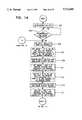
- FIGS. 14, 15 and 16illustrate the GPS interference canceler control algorithm for detecting and cancelling interference.
- FIG. 1A top-level block diagram showing the adaptive cross-polarization interference cancellation system for GPS signals is shown in FIG. 1.
- the diagramillustrates one channel or band of the invention showing the cancellation concept and illustrating the received signal composed of the combined GPS signals 1 and the interference or jamming signal 3.
- the received signal 1, 3, consisting of the GPS signals and the interference signals,is received by the antenna system 5 which effectively divides the received signals into orthogonal components VP and HP (vertically polarized and horizontally polarized) signals to the adaptive antenna feed system 7.
- a power coupler 9samples the difference port 11 of the network which provides the difference signal to the GPS receiver (not shown) via 13.
- An interference receiver detection circuit 15receives and processes the difference signal and provides the signal to adaptive control circuits 17 that control the phase modulators within the adaptive antenna feed system 7 for tilt and ellipticity.
- the loopdoses on interference to cross-polarize the feed and to null the interference to the GPS receiver.
- the GPS receivermay, optionally, provide a jam indication enable signal 19, via a GPS interface 21, to enable or disable the receiver circuit 15. When enabled, a "jam detection" signal 23 may be provided back to the GPS receiver.
- orthogonal polarization antennascan be used to match or mismatch a propagated signal using relative phase and amplitude modulations to combine the ortho components.
- the orthogonal polarization antennas within the antenna system 5can be used to mismatch the receiving system and effectively null the signal. This mismatch null would have an impact on other signals in the environment, including the desired GPS signals, by creating conditions in the antenna that could range from a perfect match to a mismatch as well.
- the loss, null or mismatch achievable using polarization mismatchcan be a value between infinity and zero.
- ⁇polarization mismatch angle, (0° ⁇ 90°).
- the polarimeter implementation utilized within the inventioneffectively modulates the orthogonal received components of both the interference signals and the GPS signals and via a detection and closed loop control creates a polarization mismatch against the interference signal in the signal path to the GPS receiver.
- FIGS. 2A-2Fshow various alternate implementation approaches possible for the invention based on representative applications for GPS receivers and GPS accuracy requirements.
- the FIGS. 2A-2Fillustrate three categories of antenna and interface implementations: (a) a single ortho antenna configuration (FIG. 2A) that can be applied to the L1 or L2 band where a single channel of nulling is implemented in either L1 or L2 bands; (b) the dual ortho antenna configurations (FIGS. 2B and 2C) using an implementation where separate L1 and L2 band antennas process the orthogonal received signals in each band for L1 hulling/cancellation and L2 bypass (FIG.
- FIG. 3depicts one preferred embodiment of a single channel dual ortho antenna configuration for nulling of L1-band (or L2-band) interference only.
- the antenna system 5provides vertically and horizontally polarized signals VP, HP to the adaptive antenna feed system 7.
- the antenna system 5includes an antenna(s) 25 which may be either a pair of L1 dipoles oriented for orthogonal operation, or one L1 microstrip patch antenna with vertical and horizontal ortho feed. Patch antenna configurations are generally known in the art.
- the antenna 25may be the novel bi-frequency antenna of FIGS. 5 and 6 which provide the L1 vertical and horizontal components for each channel.
- the antennas 25receive or detect the L1 (or L2) GPS signals along with any inband interference signals.
- the detected vertical and horizontal componentspass through band-pass filters 27, 29 and pre-amplifiers 31, 33 to provide the VP and HP signals.
- the unequal phase (or delay), or phase shift of the received ortho signals VP, HPresult from the relationship of the two received signal components and by unequal delays in the transmission lines and networks between the antennas 25 and the polarimeter 35.
- the output signals of the first hybrid 43are theoretically equal in amplitude.
- the outputs 43a, 43b of the first hybrid 43are adjusted in relative phase by variable phase control circuits 45, 47 acted upon by adaptive phase controller 49 of the adaptive control circuit 17 and then combined in the second hybrid 51 to produce a minimum null at the difference output port 53 that is effectively, or desirably, the null of the interference signal.
- the second output 55 of the hybrid 51is a summing port 55 and concurrently produces a maximum output.
- Balanced varactor phase shifter arrangements, described below,are used in each leg of the gamma (45, 47) and phi (37, 39) modulation process to provide matched operation over frequency and power.
- the difference (or delta) and summing (or sigma) outputs 53, 55 of the second hybrid junction 51are detected, processed by the interference detection receiver circuit, or receiver processing circuit, 15, and used to adaptively generate loop control signals for tilt and ellipticity (or gamma/phi) modulations by adaptive control circuit 17.
- the control loopcompensates the system for installation variations, apparent interference signal changes, and for component unbalances.
- the null or difference output 53 of the second hybrid 51is also provided to the GPS receiver, via a power coupler 9, as an input 13 with the interference signal suppressed.
- FIG. 5shows the structure of a dual ortho bi-frequency patch antenna showing two rectangular microstrip patches 61, 63 in an orthogonal arrangement.
- the dimensions D1 and D2 of the two microstrip patches, 61 and 63are the same for each patch and are selected to optimally receive the L1 and L2 bands with orthogonal linear polarizations, respectively, i.e. D1 approximately equals ⁇ 1d /2, D2 approximately equals ⁇ 2d /2, where ⁇ 1d and ⁇ 2d are the signal wavelength for L1 and L2 in the antenna dielectric, D1 is one dimension of each patch, and D2 is the second orthogonal dimension of each patch, as will be discussed further below.
- the patch antennas 61, 63may be located on a single printed circuit board.
- Patch antenna configurationsare well known in the art and generally comprise a conductive portion 65, 67 overlying an electrically thin dielectric substrate portion 69, 71 overlying a conductive Found plane 80 with feeds or probes connected with the conductive portions.
- the feed or probe locations of the patchesare selected to provide optimum linear signal coupling and cross-polarization isolation.
- four (4) feed locations 73, 75, 77, 79are used to independently provide the L2/V, L1/H, L1/V and L2/H polarization (P) electrical signals.
- FIG. 6shows an alternate structure for a dual ortho bi-frequency patch antenna showing the two rectangular microstrip patches 81, 83 in an orthogonal arrangement.
- the dimensions and orientation of the two microstrip patches, 81, 83,are the same as discussed above using a novel feed arrangement selected for frequency multiplexer operation.
- the feed or probe locations 85, 87are located along the diagonals 89, 91, or diagonal regions, of each patch and are selected to provide optimum combined signal coupling and cross-polarization isolation for L1 and L2 signals.
- Two feed locations 85, 87are used to simultaneously provide frequency multiplexed L2/V and L1/H, and L1/V and L2/H polarized electrical signals. This arrangement allows a simpler cable interface.
- the antenna approach for the preferred embodiment of the GPS interference suppression systemuses the half-wavelength microstrip rectangular element design.
- Current art microstrip antenna element techniquesinclude half-wavelength, quarter-wave, and full-wavelength element designs.
- the lengths D1 and D2 of antenna patches 61, 63are critical dimensions and are slightly less then a half-wavelength in the dielectric substrate 69, 71 material:
- D (D1 and D2)length of the microstrip element
- ⁇ rrelative dielectric constant of substrate
- ⁇ 0free-space wavelength for each frequency of interest. Variations in the dielectric constant and feed inductance makes it difficult to predict exact dimensions, so exact microstrip length is determined empirically.
- the source of radiation for a rectangular microstrip antennais the electric field excited between the edges of the microstrip element and the ground plane (excitation of a nearly infinitesimal slot with uniform E field). The fields are excited 180° out of phase between opposite edges.
- the input impedance of the antennacan be matched by using either a coaxial feed or an edge feed with a quarter-wave transformer.
- the approximate input edge impedance of a microstrip elementis given as R in ⁇ 60 ⁇ o /W, where W is the width of the slot.
- the input impedance in the embodimentis matched to 50 ⁇ impedance by using a coaxial feed. The 50 ⁇ point for the feed is obtained by varying the distance between the feed location and the edge of the element.
- the impedance of the element at the design frequency and polarizationessentially goes to zero at approximately the center symmetry line of the element
- the resultis a pair of ortho feeds.
- Each candidate feed position for 50 ⁇ impedanceis calculated for material properties and roughly located for the element. These values are used as starting points, but exact dimensions are adjusted empirically. Fabrication accuracy, materials consistency and mutual coupling result in small variations over a group of units.
- the dual-polarization rectangular microstrip elementhas dimensions selected so that D 1 matches the half-wavelength of resonant frequency, L1, and D 2 matches the half-wavelength in the dielectric of the second resonant frequency, L2.
- Each rectangular element in the embodimentcan be probed using either a one (1) feed (FIG. 6) or a two (2) independent 50 ⁇ impedance coaxial feed (FIG. 5) approach near the center of each element.
- feed 1 77will receive vertical radiated polarization for L1
- feed 2 79will receive horizontal radiated polarization for L2, and vice versa in the other element.
- the feed 87will receive a multiplexer signal composed of the sum of the vertically polarized L1 and horizontally polarized L2, and vice versa in the other element.
- the two antenna feed arrangements preferred in the inventionare: (a) one using a dual-coaxial approach for linear polarization of the two orthogonal modes of the rectangular patches resonating at two different frequencies (FIG. 5), and (b) a second using a single coaxial frequency multiplexed approach for the two orthogonal linear polarization modes of the rectangular patches (FIG. 6).
- the first approach, shown in FIG. 5,is a 4-port solution which independently optimizes the input impedance for each frequency and each polarization.
- the second approach, shown in FIG. 6,is a 2-port frequency multiplexed solution which optimizes input impedances for the two frequencies. Dual-frequency multiplexed operation can be achieved by locating the feed to each patch along a region on the diagonal of the rectangular elements.
- each element and the feed-point locationsare defined empirically using an iterative process.
- the processconsists of building the elements using the defined materials to the dimensions of the design equations for a rectangular microstrip element.
- the resonant frequency and impedanceare measured; usually differing slightly from theoretical predictions because of the combined effects of: dielectric constant variation; impedance variation for non-resonant coupling elements; feed-probe inductance; and mutual coupling.
- Adjustments to the microstrip element sizes and feed-point locationsare made to correct the resonant frequency and feed impedance, respectively. Multiple iterations may be required.
- microstrip dimensions and feed-probe locationswill be consistent (unit-to-unit) based on materials uniformity and fabrication variance.
- Feed pointsare located using the 1-dimensional current distribution of the element at the resonant frequency.
- the feed input impedance of the antennavaries proportionally with patch current and location.
- Resonant frequency and pattern of the microstrip elementare essentially independent of feed position.
- the rectangular patch's dimensionsare mechanically tuned to resonate at the L1 and L2 frequencies.
- Patch current distributionis almost sinusoidal in the direction of current and almost uniform, except near the edges, in the direction orthogonal to the current.
- a 1-volt sourceis used to excite the patch using a probe and is moved over the patch orthogonal to the dimension corresponding to the wavelength radiating edges until a point conforming to the admittance of the current for 50 ⁇ is located.
- Two symmetric 50 ⁇ solutions for each wavelengthexist between the center and the edges. Coupling between feeds is minimum due to mode orthogonality.
- the polarization of the multiplexed, or diagonally located, feedsis trickier to position.
- the precise polarization at resonancechanges slightly with location and the impedance point has to be systematically adjusted.
- the measurementscan use either of two test setups: a standard slotted-line; or an automatic network analyzer.
- the looking-in reflection coefficient versus frequencyis measured.
- the standing-wave ratio magnitude and minimum position relative to the patchare recorded and plotted using a Smith chart. From this reflection coefficient locus, the resonant frequency and power factor of the patch is determined using graphical techniques.
- the power factor(the reciprocal of the Q) is convenient for resonant circuit representation and analysis.
- the Smith chart representationshows the admittance locus of the feed versus frequency for the resonant circuit.
- the input impedanceis generally measured for discrete frequencies in a band around the wavelength of interest after calibration of the Smith chart by putting a short circuit at the plane where the line connects to the patch.
- the probe or lead locations 77 (L1 polarization 1) and 79 (L2 polarization 2) for the antenna 63 of FIG. 5is determined as follows: The probe location 77 lies along the O ⁇ location near the center line for the D2 length and the probe location is moved orthogonally to the D2 direction until the 50 ⁇ impedance is located, as shown. Similarly the probe location 79 lies along the O ⁇ location near the center line for the D1 length and the probe location is moved orthogonally to the D1 direction until the 50 ⁇ impedance is located, as shown.
- the probe or lead locations 73, 75 of the antenna 61is determined in the same manner.
- the probe or lead location 87is at the locus of points where 50 ⁇ impedance is calculated for each of the L1 and L2 frequencies and essentially at a diagonal or diagonal region.
- FIG. 8Ashowing the RF block diagram and receiver processing schematic for one channel implementation of GPS interference cancellation at frequency L1.
- the illustrated inputis a pair of orthogonal RF signals from the antennas 25, or from the antennas of FIGS. 5 and 6.
- the cancellation approachis functionally composed of the following: the antenna system 5; the adaptive antenna feed system 7; a power coupler 9; the interference receiver and detection circuit 15; and the adaptive control circuit 17.
- FIG. 8further illustrates the hardware partition and fabrication approach of the invention into the following physical units: a microwave section 101; a down converter section 103; a receiver/detector section 105; and a system control section 107.
- the down converter 103 and receiver detector channel 105monitor a coupled delta or difference port 109 of the microwave section 101.
- the microwave section 101 shownconsists of band-pass filters 27, 29 and preamplifiers 31, 33 which interface with the ortho antennas, a solid state polarimeter or gamma/phi modulator 35, a delta port power divider/coupler 9, and a delta monitor port RF amplifier 10.
- Channel bandwidth and noise figureare set by the arrangement of bandpass filters 27, 29 and low noise RF preamplifiers 31, 33.
- the filters and preamplifiersare generally located with the antenna (25, FIG. 5, FIG.
- the polarimeter modulator or gamma/phi modulator 35utilizes a 90-degree hybrid architecture, as will be described. Two sets of gamma and phi modulator controls 111, 113 are utilized to control the tilt and ellipticity of the polarimeter 35, and the polarimeter provides a delta 53 and a sigma 55 output port. The sigma output 55 of the polarimeter is terminated and is not used in the system.
- the delta port output 53 of the polarimeter 35is sampled in an RF power divider/coupler 9.
- One output port 13 of the power divideris provided as the input to the GPS receiver and includes the GPS received signals of interest with interference suppressed.
- the second output port 110is the null monitor port and is amplified in an L1-band RF amplifier 10 and provided for signal processing and detection and used to adaptively generate null loop control signals for tilt and ellipticity modulation.
- the interference receiver detection circuit 15, as shown,consists of a downconverter 103 and receiver/detector 105.
- the signal detection and processing portion of the inventionprovides dynamic range control via AGC and video detected null signals for system control section processing.
- the adaptive system control section 107is digital signal processing composed of the signal A/D converters (ADC) 115 or encoder, via a multiplexer 117, signal processing and loop control algorithm in a microcontroller 119, and control signal D/A converters (DAC) 121 for analog drive to the modulator 35.
- ADCsignal A/D converters
- DACcontrol signal D/A converters
- the output of the microcontroller and control program/algorithmconsist of iterative settings for the AGC amplifier, and (four) gamma/phi phase shift control signals. These signals are D/A converted at 121 and applied to the respective devices as analog control signals to complete loop closure.
- the control loop and signal processing algorithmcompensate the system for apparent interference signal polarization orthogonality, interference signal properties, polarization changes and component unbalance, as will be described.
- the null output 53 of the second hybridis provided to the GPS receiver at 13 as an input with the interference signal suppressed.
- FIG. 8Bdepicts an alternative interference receiver detection circuit that is much simpler and preferred. It is essentially a logarithmic amplifier having a log video output provided directly to the A/D converter 115. The alternative circuit reduces the need for AGC.
- FIG. 9shows the detail of the polarimeter modulator 35 used in the adaptive antenna feed system 7.
- the modulator shownutilizes a 90-degree hybrid architecture.
- the polarimeteris composed of two 90-degree hybrid junctions 43, 51 and two pair of gamma 45, 47 and phi 37, 39 phase shift modulators. Each phase shifter is adjustable over a minimum 0-180 degree range.
- the first pair of balanced RF phase shifters 37, 39is located in the ortho lines from the antenna prior to the first 90-degree hybrid 43 and sets the tilt angle, or phi, of the polarimeter 35.
- phase shiftersare set to relative quadrature and compensate for phase and delay unbalances in each leg of the antenna's orthogonal paths, as well as imbalances and imperfections in subsequent hybrids and modulators.
- the phase shifter output signals from 37, 39are combined in the first hybrid junction 43.
- the output signals of the first hybrid 43are each theoretically equal in amplitude (i.e. the difference in amplitude is at a minimum).
- the outputs 43a, 43b of the first hybrid 43are adjusted in relative phase by the second pair of balanced phase shift modulators 45, 47 and combined in the second 90-degree hybrid 51 to produce a voltage null or signal minima at one output port 53 of the hybrid, termed the delta port, that is effectively the voltage null of the interference signal.
- the second pair of RF phase shifters 45, 47set the ellipticity, or gamma, of the polarimeter 35.
- the alternate output of the second hybridtermed the sigma port, concurrently produces a voltage peak or maxima output.
- Balanced varactor phase shifter arrangements, to be described,are used in each leg of the gamma and phi modulation process to provide matched modulator operation over frequency and signal level
- the delta port output 53 of the second hybrid junction 51is power divided in an RF power divider/coupler 9.
- the polarimeter, or gamma/phi modulatormay be further described, as follows. Assume that the orthogonal VP and HP components may be represented by E 1 cos ⁇ t and E 2 cos ⁇ t+ ⁇ .
- the phase shift a between E 1 and E 2represents the net phase difference introduced into an orthogonally polarized system by the relationship of the two received signal elements and by unequal delays in the transmission lines and networks between the antenna(s) and the polarization unit.
- the phi phase shifters 37, 39adjust the components so that ⁇ is cancelled.
- the outputs of the first hybrid 43, on 43a and 43bare roughly equal in amplitude with opposite phase angles with respect to (E 1 -90°) and E 1 .
- the gamma phase shifters 45, 47adjust the signals at 43a, 43b so that they become 90-degrees apart and the second hybrid junction 51 further shifts and combines the inputs thereto so that they are 180-degrees out of phase, thereby producing a zero null.
- the phase shifts phi and gammaare adjusted to compensate for unbalances in the system to produce a minimum null signal at the delta port.
- the adjustment of the phi from its nominal valueeffectively compensates for the mismatch condition to produce a minimum null at delta port 53.
- the adjustment of the angle gammaeffectively compensates for amplitude imbalances to produce a minimum null at delta port 53.
- FIG. 10shows the downconverter 103 schematic.
- the diagramillustrates the local oscillator 131, a single sideband image rejection mixer 133 and IF amplifier 135 configuration, a bandpass filter 137 at IF, a second IF amplifier 139, and a lowpass filter 141.
- the downconverteruses a local oscillator (LO) 131 at 1,586 Mhz and converts L1 to a 10 Mhz IF with 2 MHz bandwidth using a single sideband mixer configuration.
- the IF outputgoes through a bandpass filter 137 and is amplified in a second IF amplifier stage 139 and lowpass filtered 141 to set the receiver dynamic range.
- LOlocal oscillator
- FIG. 11showing the receiver/detector 105 schematic.
- the diagramillustrates the downconverter signal as an input to a 2 MHz bandpass filter 143 at 10 MHz, an Automatic Gain Control (AGC) controlled linear IF amplifier 145, a gain/driver amplifier 147, video detection stage 149 with separate wideband and narrowband video filters 151, 153.
- AGCAutomatic Gain Control
- AGCis used in the linear scheme to obtain sufficient dynamic range to process the extent of anticipated interference signals.
- Both wideband and narrowband detected video signals 151a, 153aare A/D converted and processed by the acquisition and tracking algorithm in a microcontroller 119.
- FIG. 12showing an alternative logarithmic or exponential IF amplifier approach (see FIG. 8B) which is advantageous since it obtains the needed dynamic range using no AGC, or a small AGC range.
- This arrangementincludes three cascaded stages of amplifiers 110, 112, 114 with three detectors 116, 118, 120 that are summed via 122 and provided directly to the A/D converter 115.
- This logarithmic amplifierimproves interference receiver and detection performance by expanding operating dynamic range for interference and null detection.
- Modifications on the inventionmay include asymmetric gamma/phi phase shifter organization for a simplified modulator arrangement; and a 180-degree/90-degree hybrid polarimeter architecture.
- FIG. 13showing a variable varactor controlled analog phase shifter schematic portion of the RF polarimeter 35.
- the variable phase shifter structureis used for each of the four 0-180 degree balanced gamma/phi modulators 37, 39, 45, 47 in the polarimeter 35.
- the schematic diagramillustrates a reflective hybrid implementation using two varactor tuned phase shifter diodes 120, 122 which produce a variable transmission line phase shift with constant time delay.
- the phase shiftis twice the electrical length through the varactor to ground.
- the control voltage inputsare the gamma and phi voltages from digital to analog converter 121.
- FIGS. 14-16are flow charts describing the steps utilized by the microprocessor controller 119 for detecting and cancelling interference and/or jamming signals.
- the basic system stepsinclude a preliminary built-in-test loop, a phase scan to determine interference signal presence, a coarse and fine loop to cancel and dose on interference, and a maintenance procedure to detect and adjust the interference null to changes. Detection of interference is based on exceeding a jam or interference threshold.
- the algorithmcoarsely adjusts the polarimeter to null the interference signal, followed by a fine adjustment of the polarimeter to maximize the null to the GPS receiver.
- the coarse scanutilizes a phase resolution commensurate with the size and shape of the achievable null phenomena and the spectral/temporal properties of the interference signal.
- the microprocessor 119monitors the difference or delta port 53 via the power divider 9 and the RF amplifier 10. This delta nulling port signal over line 109 is processed by the receiver detection circuit 15 and converted to digital form through the analog to digital converter 115.
- the first stepis an initialization and BIT (built-in test) step to verify the DC voltages applied to the various circuit boards and to determine that the analog-to-digital and digital-to-analog converters are operational, and any other initialization that may be required, as functionally depicted in block 301.
- the systemdetermines if an interference or a jam signal is present (block 303).
- the presence of an interference or jam signalis determined by looking at the magnitude of the voltage of the delta port hulling signal (over line 109, as processed) to determine if the voltage is above a predetermined voltage threshold for normal GPS signals. If the voltage is above the predetermined threshold, interference or jamming is determined to exist. If interference and/or jamming is detected, the phi 1 and phi 2 phase shifts for phase shifters 39, 37 are set at zero degrees (block 305). This is done by setting the control voltage to the phase shifters 39, 37 (see FIG. 13) to a predetermined voltage that corresponds to zero degrees. Typically, there is a linear relationship between the control voltage and the amount of phase shifting, which is determined empirically.
- the gamma 1 signal to phase shifter 47is sequentially set to 0, 45, 90, 135, and 180 degrees and for each setting, the gamma 2 input to phase shifter 45 is scanned from 0 to 180 degrees in 2.5-degree increments.
- the delta port nulling signalis monitored and the output voltage is stored at each scan point (block 309).
- the gamma 1 and 2 control voltagesare provided to phase shifters 47 and 45 to set the control voltages to levels that produced the minimum output at the delta port (block 311).
- the phi 2 voltage signal to phase shifter 37is repetitively set at 0, 45, 90, 135, and 180 degrees and, at each setting, the phi 1 control voltage to phase shifter 39 is scanned from 0 to 180-degrees in 2.5-degree steps (block 313). Again the delta port hulling signal is monitored at each setting and the output voltage is stored (block 315). Then, the phi 1 and phi 2 control voltages are provided to phase shifters 39 and 37 to voltage levels that produced the minimum output at the delta nulling port (block 317).
- the systemcontinues by setting an alpha and rho value of 22.5 and 0.35 respectively (block 319).
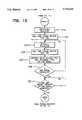
- a fine tuning routineis then called (block 321) as shown in FIG. 16.
- the fine tuning routinescans gamma 1 i.e. provides control voltages to phase shifter 47 over a range from alpha degrees below to alpha degrees above the current setting of gamma 1 in rho degree increments (block 401).
- the delta nulling portis monitored and the output voltages are stored at each scan point (block 403).
- the systemdetermines the control voltage settings for gamma 1 that produce the minimum output at the delta port (block 405).
- Gamma 1is then set to this control voltage (block 407).
- the systemthen scans or sets phi 1 from alpha degrees below to alpha degrees above the current setting of phi 1 and scans or incrementally sets the control voltage in rho degree increments (block 409). During this scanning, the delta nulling port is monitored and the output voltage is stored for each scanned point (block 411). The system then determines the control voltage setting for phi 1 that produced the minimum output at the delta nulling port (block 413). Phi 1 is then set to this control voltage (block 415). The fine tuning routine is then completed and there is a return to block 321 of FIG. 15.
- phase shiftershave been set so as to produce a minimum output signal at the delta port representative of the GPS signal with the interference removed or suppressed.
- the systemcontinues to monitor the nulling port output to determine the signal level (block 327).
- the systemdetermines whether the interference or jam signal has been cancelled by determining if the delta hulling port output voltage moves a predetermined amount higher than the set minimum (decision block 329). If a voltage change has occurred, the system then determines if a new jam or interference signal is present or changed (decision block 331). If it has been changed, a return is made to block 305 of FIG. 14 to begin a new search for a minimum output at the delta port.
- the fine tuningcontinues by returning to decision block 323.
- the delta hulling port output voltageis at a minimum value of 100 mv, typical for GPS signals.
- the system and GPS receiverare on a moving vehicle such as a truck. If the truck moves, the phase shifting may occur due to truck motion which will result in the delta hulling port signal changing due to phase shifts. However, the change is not normally in excess of a predetermined value. For example, by a movement of the receiver, the output voltage may change from 100 millivolts to 1 volt.
- the fine tuning routineis again called but at the "finer" alpha and rho values (block 323) to continually change the phase shift signals to maintain a minimum or null voltage at the delta port.
- the level of the delta port signalbecomes significant or "large” (as determined in decision blocks 329, 331) such as the 100 millivolt signal rising to, say, 5 volts, it is determined that a new jam or interference signal is present and the overall system starts anew beginning at decision block 305.
- FIG. 4showing a second preferred embodiment of the invention utilizing a dual ortho bi-frequency antenna configuration for nulling of L1 interference and L2 bypass. Illustrated in FIG. 4 is the same polarimeter and control architecture as in FIG. 3.
- the antenna 225 utilized for the implementationare two rectangular microstrip patches in an orthogonal arrangement such that they receive the L1 and L2 bands with orthogonal linear polarizations, respectively as are shown and described in FIG. 5 (or FIG. 6).
- the null output of the second hybrid, from power coupler 9is combined with a RHCP bypass signal generated for L2 band (or the output of a parallel hulling circuit for the L2 band).
- the L2 vertical and horizontal components from antennas 61, 63are provided to a 90-degree hybrid junction 227 whereby the orthogonal signal components are combined, then through a band-pass filter 229 at the L2 frequency, through pre-amplifier 231 to produce the L2 bypass signal over line 233.
- the combined signal output, L1 and L2is provided to the GPS receiver, via diplexer 235, as an input with the interference signal suppressed.
- FIGS. 2A-2Fvarious other configurations, including, but not limited to the configurations of FIGS. 2A-2F, may be implemented in accordance with the present invention.
- a configurationsimilar to FIG. 4, could be arranged for L2 band interference cancellation with L1 bypass.
- the patch antenna arrangements of FIGS. 5 and 6may be used with any of the configurations of FIGS. 2A-2F.
- the patch antenna configuration of FIG. 5, for example,provides for L1 orthogonal vertical and horizontal components and L2 orthogonal vertical and horizontal components and each of these components, or only a set of L1 or L2 components may be needed, depending on the configuration chosen.
Landscapes
- Engineering & Computer Science (AREA)
- Radar, Positioning & Navigation (AREA)
- Remote Sensing (AREA)
- Computer Networks & Wireless Communication (AREA)
- Physics & Mathematics (AREA)
- General Physics & Mathematics (AREA)
- Signal Processing (AREA)
- Astronomy & Astrophysics (AREA)
- Aviation & Aerospace Engineering (AREA)
- Position Fixing By Use Of Radio Waves (AREA)
- Radio Relay Systems (AREA)
- Variable-Direction Aerials And Aerial Arrays (AREA)
Abstract
Description
D≈0.49λ.sub.d =0.49λ.sub.0 /(ε.sub.r).sup.1/2
Claims (15)
Priority Applications (8)
| Application Number | Priority Date | Filing Date | Title |
|---|---|---|---|
| US08/608,493US5712641A (en) | 1996-02-28 | 1996-02-28 | Interference cancellation system for global positioning satellite receivers |
| DE19781627ADE19781627C2 (en) | 1996-02-28 | 1997-02-13 | Interference cancellation system for global, satellite-based location receivers |
| IL12564197AIL125641A (en) | 1996-02-28 | 1997-02-13 | Interference cancellation system for global positioning satellite receivers |
| CA002245872ACA2245872C (en) | 1996-02-28 | 1997-02-13 | Interference cancellation system for global positioning satellite receivers |
| DE19781627TDE19781627T1 (en) | 1996-02-28 | 1997-02-13 | Interference cancellation system for global, satellite-based location receivers |
| PCT/US1997/002348WO1997032405A1 (en) | 1996-02-28 | 1997-02-13 | Interference cancellation system for global positioning satellite receivers |
| AU19590/97AAU1959097A (en) | 1996-02-28 | 1997-02-13 | Interference cancellation system for global positioning satellite receivers |
| GB9817098AGB2325594B (en) | 1996-02-28 | 1997-02-13 | Interference cancellation system for global positioning satellite receivers |
Applications Claiming Priority (1)
| Application Number | Priority Date | Filing Date | Title |
|---|---|---|---|
| US08/608,493US5712641A (en) | 1996-02-28 | 1996-02-28 | Interference cancellation system for global positioning satellite receivers |
Publications (1)
| Publication Number | Publication Date |
|---|---|
| US5712641Atrue US5712641A (en) | 1998-01-27 |
Family
ID=24436731
Family Applications (1)
| Application Number | Title | Priority Date | Filing Date |
|---|---|---|---|
| US08/608,493Expired - LifetimeUS5712641A (en) | 1996-02-28 | 1996-02-28 | Interference cancellation system for global positioning satellite receivers |
Country Status (7)
| Country | Link |
|---|---|
| US (1) | US5712641A (en) |
| AU (1) | AU1959097A (en) |
| CA (1) | CA2245872C (en) |
| DE (2) | DE19781627C2 (en) |
| GB (1) | GB2325594B (en) |
| IL (1) | IL125641A (en) |
| WO (1) | WO1997032405A1 (en) |
Cited By (85)
| Publication number | Priority date | Publication date | Assignee | Title |
|---|---|---|---|---|
| US5872540A (en)* | 1997-06-26 | 1999-02-16 | Electro-Radiation Incorporated | Digital interference suppression system for radio frequency interference cancellation |
| WO1999057572A1 (en)* | 1998-05-01 | 1999-11-11 | Novatel Inc. | Method and apparatus for characterizing multipath interference in circularly polarized signals |
| US6115409A (en)* | 1999-06-21 | 2000-09-05 | Envoy Networks, Inc. | Integrated adaptive spatial-temporal system for controlling narrowband and wideband sources of interferences in spread spectrum CDMA receivers |
| EP1035664A1 (en)* | 1999-03-12 | 2000-09-13 | ICO Services Ltd. | Satellite communication system with interference mitigation |
| US6141371A (en)* | 1996-12-18 | 2000-10-31 | Raytheon Company | Jamming suppression of spread spectrum antenna/receiver systems |
| US6166690A (en)* | 1999-07-02 | 2000-12-26 | Sensor Systems, Inc. | Adaptive nulling methods for GPS reception in multiple-interference environments |
| US6175327B1 (en)* | 1999-01-16 | 2001-01-16 | Sensors Systems, Inc. | GPS receivers with adaptive antenna systems for suppressing interference signals |
| US6204810B1 (en) | 1997-05-09 | 2001-03-20 | Smith Technology Development, Llc | Communications system |
| US6252553B1 (en) | 2000-01-05 | 2001-06-26 | The Mitre Corporation | Multi-mode patch antenna system and method of forming and steering a spatial null |
| US6388610B1 (en)* | 1998-01-23 | 2002-05-14 | The Charles Stark Draper Laboratory, Inc. | Antijam null steering conformal cylindrical antenna system |
| US20020061080A1 (en)* | 2000-10-13 | 2002-05-23 | Richards James L. | Method and system for reducing potential interference in an impulse radio |
| WO2002009231A3 (en)* | 2000-07-26 | 2002-06-20 | Western Multiplex Corp | Adaptive array antenna nulling |
| US20020086601A1 (en)* | 2000-11-08 | 2002-07-04 | Marvin Lewis | Crochet-knitted mattress closing tape |
| US6480151B2 (en) | 2000-12-29 | 2002-11-12 | Lockheed Martin Corporation | GPS receiver interference nuller with no satellite signal distortion |
| US6529568B1 (en)* | 2000-10-13 | 2003-03-04 | Time Domain Corporation | Method and system for canceling interference in an impulse radio |
| US20030043086A1 (en)* | 2001-08-30 | 2003-03-06 | Hrl Laboratories, Llc | Antenna system and RF signal interference abatement method |
| US6639541B1 (en) | 2000-08-29 | 2003-10-28 | The United States Of America As Represented By The Secretary Of The Navy | Device and method for detecting, measuring, and reporting low-level interference at a receiver |
| US20030214443A1 (en)* | 2002-03-15 | 2003-11-20 | Bauregger Frank N. | Dual-element microstrip patch antenna for mitigating radio frequency interference |
| US20040031723A1 (en)* | 2002-06-20 | 2004-02-19 | L'oreal | Adhesive applicator for fixing to the end of a finger |
| US20040042569A1 (en)* | 2002-09-03 | 2004-03-04 | Electro-Radiation Incorporated | Method and apparatus to provide communication protection technology for satellite earth stations |
| US6703974B2 (en) | 2002-03-20 | 2004-03-09 | The Boeing Company | Antenna system having active polarization correlation and associated method |
| US6710739B1 (en) | 2003-01-03 | 2004-03-23 | Northrop Grumman Corporation | Dual redundant GPS anti-jam air vehicle navigation system architecture and method |
| US20040104843A1 (en)* | 2002-02-27 | 2004-06-03 | Masahiro Mimura | Polarized wave measuring apparatus, and antenna characteristic measuring apparatus and radio wave measuring apparatus using the same |
| US6825804B1 (en)* | 2003-07-09 | 2004-11-30 | Rockwell Collins, Inc. | Interference-aided navigation with cyclic jammer cancellation |
| EP1491910A1 (en)* | 2003-06-27 | 2004-12-29 | Seiko Epson Corporation | Radio receiver and GPS receiver |
| US6861983B2 (en) | 2001-12-04 | 2005-03-01 | Electro Radiation, Inc. | Method and apparatus for reducing electromagnetic interference and jamming in GPS equipment operating in rolling environments |
| US20050114074A1 (en)* | 2003-01-13 | 2005-05-26 | Green Francisco R. | Tunable filter device for spatial positioning systems |
| WO2005057808A3 (en)* | 2003-12-03 | 2005-07-14 | Raytheon Co | Beamforming in a gps receiver |
| US6961017B1 (en) | 2003-12-16 | 2005-11-01 | Lockheed Martin Corporation | Apparatus for providing anti-jamming capability to legacy GPS receivers |
| US20050259760A1 (en)* | 2004-05-21 | 2005-11-24 | Casabona Mario M | Method and apparatus for excision of narrowband interference signals in navigation or communication bands |
| US20070047678A1 (en)* | 2005-08-30 | 2007-03-01 | Motorola, Inc. | Method and system for combined polarimetric and coherent processing for a wireless system |
| US20070066226A1 (en)* | 2005-09-21 | 2007-03-22 | Samsung Electronics Co., Ltd. | Apparatus and method for interference cancellation in wireless mobile stations operating concurrently on two or more air interfaces |
| US20070274712A1 (en)* | 2005-12-08 | 2007-11-29 | Ralph Leppla | Method for detecting and localizing faults in an optical transmission path, and optical transmission system |
| US20080175340A1 (en)* | 2007-01-23 | 2008-07-24 | Infineon Technologies Agst.-Martin-Str.53 Munich, Germany 81669 | Wireless communication device and method for reducing in-band interference in a gps receiver |
| US20080284672A1 (en)* | 2007-05-16 | 2008-11-20 | Infineon Technologies Ag | Configurable Radio Frequency Element |
| US20090203312A1 (en)* | 2006-01-10 | 2009-08-13 | Pieter Van Rooyen | Method and system for antenna geometry for multiple antenna handsets |
| US20100001904A1 (en)* | 2008-07-02 | 2010-01-07 | Fujitsu Limited | Radio communication apparatus and system |
| US7715722B1 (en)* | 2006-01-27 | 2010-05-11 | Lockheed Martin Corporation | Fiber optic radio frequency distribution system |
| USRE41382E1 (en) | 2003-06-18 | 2010-06-22 | General Dynamics C4 Systems, Inc. | Method and system for detecting interference for global positioning systems |
| US20100278197A1 (en)* | 2007-03-12 | 2010-11-04 | Comba Telecom System (China) Ltd. | Double frequency combiner |
| US20110298667A1 (en)* | 2006-12-04 | 2011-12-08 | Nuttawit Surittikul | Method of Operating A Patch Antenna In A Single Higher Order Mode |
| TWI382272B (en)* | 2008-06-25 | 2013-01-11 | Nat Applied Res Laboratories | Satellite optical lens |
| WO2013130818A1 (en)* | 2012-02-28 | 2013-09-06 | Physical Devices Llc | Methods, systems, and computer readable media for mitigation of in-band interference of global positioning system (gps) signals |
| US8666347B2 (en) | 2010-10-14 | 2014-03-04 | Physical Devices, Llc | Methods and devices for reducing radio frequency interference |
| US20140062502A1 (en)* | 2012-08-29 | 2014-03-06 | Hitachi, Ltd | Method for identifying emi sources in an electrical system |
| US9042857B2 (en) | 2010-08-30 | 2015-05-26 | Physical Devices, Llc | Methods, systems, and non-transitory computer readable media for wideband frequency and bandwidth tunable filtering |
| US9087851B2 (en) | 2013-05-22 | 2015-07-21 | International Business Machines Corporation | Silicon-based electronics with disabling feature |
| US9106286B2 (en) | 2000-06-13 | 2015-08-11 | Comcast Cable Communications, Llc | Network communication using diversity |
| US20150270821A1 (en)* | 2013-01-11 | 2015-09-24 | International Business Machines Corporation | Variable load for reflection-type phase shifters |
| US9184498B2 (en) | 2013-03-15 | 2015-11-10 | Gigoptix, Inc. | Extending beamforming capability of a coupled voltage controlled oscillator (VCO) array during local oscillator (LO) signal generation through fine control of a tunable frequency of a tank circuit of a VCO thereof |
| US9275690B2 (en) | 2012-05-30 | 2016-03-01 | Tahoe Rf Semiconductor, Inc. | Power management in an electronic system through reducing energy usage of a battery and/or controlling an output power of an amplifier thereof |
| US9350401B2 (en) | 2010-08-30 | 2016-05-24 | Physical Devices, Llc | Tunable filter devices and methods |
| US9423484B2 (en) | 2013-10-22 | 2016-08-23 | Polaris Sensor Technologies, Inc. | Sky polarization and sun sensor system and method |
| US9459987B2 (en) | 2014-03-31 | 2016-10-04 | Intuit Inc. | Method and system for comparing different versions of a cloud based application in a production environment using segregated backend systems |
| US9473481B2 (en) | 2014-07-31 | 2016-10-18 | Intuit Inc. | Method and system for providing a virtual asset perimeter |
| US9501345B1 (en) | 2013-12-23 | 2016-11-22 | Intuit Inc. | Method and system for creating enriched log data |
| US9509351B2 (en) | 2012-07-27 | 2016-11-29 | Tahoe Rf Semiconductor, Inc. | Simultaneous accommodation of a low power signal and an interfering signal in a radio frequency (RF) receiver |
| US9516064B2 (en)* | 2013-10-14 | 2016-12-06 | Intuit Inc. | Method and system for dynamic and comprehensive vulnerability management |
| US9531070B2 (en) | 2013-03-15 | 2016-12-27 | Christopher T. Schiller | Extending beamforming capability of a coupled voltage controlled oscillator (VCO) array during local oscillator (LO) signal generation through accommodating differential coupling between VCOs thereof |
| US9596251B2 (en) | 2014-04-07 | 2017-03-14 | Intuit Inc. | Method and system for providing security aware applications |
| US9666942B2 (en) | 2013-03-15 | 2017-05-30 | Gigpeak, Inc. | Adaptive transmit array for beam-steering |
| US9686301B2 (en) | 2014-02-03 | 2017-06-20 | Intuit Inc. | Method and system for virtual asset assisted extrusion and intrusion detection and threat scoring in a cloud computing environment |
| US9716315B2 (en) | 2013-03-15 | 2017-07-25 | Gigpeak, Inc. | Automatic high-resolution adaptive beam-steering |
| US9722310B2 (en) | 2013-03-15 | 2017-08-01 | Gigpeak, Inc. | Extending beamforming capability of a coupled voltage controlled oscillator (VCO) array during local oscillator (LO) signal generation through frequency multiplication |
| US9742794B2 (en) | 2014-05-27 | 2017-08-22 | Intuit Inc. | Method and apparatus for automating threat model generation and pattern identification |
| US9780449B2 (en) | 2013-03-15 | 2017-10-03 | Integrated Device Technology, Inc. | Phase shift based improved reference input frequency signal injection into a coupled voltage controlled oscillator (VCO) array during local oscillator (LO) signal generation to reduce a phase-steering requirement during beamforming |
| US9806790B2 (en) | 2010-03-29 | 2017-10-31 | Odyssey Wireless, Inc. | Systems/methods of spectrally efficient communications |
| US9837714B2 (en) | 2013-03-15 | 2017-12-05 | Integrated Device Technology, Inc. | Extending beamforming capability of a coupled voltage controlled oscillator (VCO) array during local oscillator (LO) signal generation through a circular configuration thereof |
| US9866267B2 (en) | 2014-02-21 | 2018-01-09 | Physical Devices, Llc | Devices and methods for diversity signal enhancement and cosite cancellation |
| US9866581B2 (en) | 2014-06-30 | 2018-01-09 | Intuit Inc. | Method and system for secure delivery of information to computing environments |
| US9900322B2 (en) | 2014-04-30 | 2018-02-20 | Intuit Inc. | Method and system for providing permissions management |
| US9923909B2 (en) | 2014-02-03 | 2018-03-20 | Intuit Inc. | System and method for providing a self-monitoring, self-reporting, and self-repairing virtual asset configured for extrusion and intrusion detection and threat scoring in a cloud computing environment |
| US20180224557A1 (en)* | 2014-09-05 | 2018-08-09 | The Board Of Trustees Of The Leland Stanford Junior University | Spoofing detection and anti-jam mitigation for gps antennas |
| US10102082B2 (en) | 2014-07-31 | 2018-10-16 | Intuit Inc. | Method and system for providing automated self-healing virtual assets |
| US20200007172A1 (en)* | 2018-06-29 | 2020-01-02 | Renesas Electronics Corporation | Communication device |
| US10725182B2 (en) | 2018-01-04 | 2020-07-28 | Interstate Electronics Corporation | Systems and methods for providing anti-spoofing capability to a global navigation satellite system receiver |
| US10757133B2 (en) | 2014-02-21 | 2020-08-25 | Intuit Inc. | Method and system for creating and deploying virtual assets |
| WO2020176484A1 (en) | 2019-02-26 | 2020-09-03 | Bae Systems Information And Electronic Systems J Integration Inc. | Circular patch array for anti-jam gps |
| US10873404B2 (en)* | 2017-07-13 | 2020-12-22 | Benjamin J. Egg | System and method for digital direction finding |
| US11294700B2 (en) | 2014-04-18 | 2022-04-05 | Intuit Inc. | Method and system for enabling self-monitoring virtual assets to correlate external events with characteristic patterns associated with the virtual assets |
| US20220329268A1 (en)* | 2021-04-07 | 2022-10-13 | Skyworks Solutions, Inc. | Systems and methods for diplexer circuits with leakage cancellation |
| US11698461B1 (en) | 2019-11-20 | 2023-07-11 | Telephonics Corp. | GPS denial detection and reporting and mitigation |
| US12009915B2 (en) | 2021-01-29 | 2024-06-11 | Eagle Technology, Llc | Compact receiver system with antijam and antispoof capability |
| WO2024241310A3 (en)* | 2023-05-23 | 2025-01-09 | Infinidome Ltd. | Anti-jamming using dual channel multi-frequency null-steering approach |
| US12392904B2 (en) | 2023-01-16 | 2025-08-19 | Rockwell Collins, Inc. | Controlled radiation pattern antenna for jamming/spoofing resistant airborne GNSS sensors |
Families Citing this family (2)
| Publication number | Priority date | Publication date | Assignee | Title |
|---|---|---|---|---|
| CN113991325B (en)* | 2021-12-27 | 2022-04-08 | 中国人民解放军海军工程大学 | A Design Method of Interference Cancellation Space Sampling Antenna for Satellite Communication Ground Station |
| CN118731985B (en)* | 2024-08-30 | 2024-11-29 | 广东工业大学 | Co-channel interference resistant circuit for satellite navigation terminal |
Citations (6)
| Publication number | Priority date | Publication date | Assignee | Title |
|---|---|---|---|---|
| US3421691A (en)* | 1966-08-02 | 1969-01-14 | American Standard Inc | Boiler temperature modulating control |
| US3883872A (en)* | 1973-06-28 | 1975-05-13 | Nasa | System for interference signal nulling by polarization adjustment |
| US4283795A (en)* | 1979-10-03 | 1981-08-11 | Bell Telephone Laboratories, Incorporated | Adaptive cross-polarization interference cancellation arrangements |
| US5298908A (en)* | 1987-11-27 | 1994-03-29 | Unisys Corporation | Interference nulling system for antennas |
| US5485485A (en)* | 1992-04-10 | 1996-01-16 | Cd Radio Inc. | Radio frequency broadcasting systems and methods using two low-cost geosynchronous satellites and hemispherical coverage antennas |
| US5515057A (en)* | 1994-09-06 | 1996-05-07 | Trimble Navigation Limited | GPS receiver with N-point symmetrical feed double-frequency patch antenna |
- 1996
- 1996-02-28USUS08/608,493patent/US5712641A/ennot_activeExpired - Lifetime
- 1997
- 1997-02-13CACA002245872Apatent/CA2245872C/ennot_activeExpired - Lifetime
- 1997-02-13WOPCT/US1997/002348patent/WO1997032405A1/enactiveApplication Filing
- 1997-02-13DEDE19781627Apatent/DE19781627C2/ennot_activeExpired - Lifetime
- 1997-02-13DEDE19781627Tpatent/DE19781627T1/enactiveGranted
- 1997-02-13AUAU19590/97Apatent/AU1959097A/ennot_activeAbandoned
- 1997-02-13GBGB9817098Apatent/GB2325594B/ennot_activeExpired - Lifetime
- 1997-02-13ILIL12564197Apatent/IL125641A/ennot_activeIP Right Cessation
Patent Citations (6)
| Publication number | Priority date | Publication date | Assignee | Title |
|---|---|---|---|---|
| US3421691A (en)* | 1966-08-02 | 1969-01-14 | American Standard Inc | Boiler temperature modulating control |
| US3883872A (en)* | 1973-06-28 | 1975-05-13 | Nasa | System for interference signal nulling by polarization adjustment |
| US4283795A (en)* | 1979-10-03 | 1981-08-11 | Bell Telephone Laboratories, Incorporated | Adaptive cross-polarization interference cancellation arrangements |
| US5298908A (en)* | 1987-11-27 | 1994-03-29 | Unisys Corporation | Interference nulling system for antennas |
| US5485485A (en)* | 1992-04-10 | 1996-01-16 | Cd Radio Inc. | Radio frequency broadcasting systems and methods using two low-cost geosynchronous satellites and hemispherical coverage antennas |
| US5515057A (en)* | 1994-09-06 | 1996-05-07 | Trimble Navigation Limited | GPS receiver with N-point symmetrical feed double-frequency patch antenna |
Cited By (146)
| Publication number | Priority date | Publication date | Assignee | Title |
|---|---|---|---|---|
| US6141371A (en)* | 1996-12-18 | 2000-10-31 | Raytheon Company | Jamming suppression of spread spectrum antenna/receiver systems |
| US6204810B1 (en) | 1997-05-09 | 2001-03-20 | Smith Technology Development, Llc | Communications system |
| US6271790B2 (en) | 1997-05-09 | 2001-08-07 | Smith Technology Development Llc | Communication system |
| US5872540A (en)* | 1997-06-26 | 1999-02-16 | Electro-Radiation Incorporated | Digital interference suppression system for radio frequency interference cancellation |
| US6388610B1 (en)* | 1998-01-23 | 2002-05-14 | The Charles Stark Draper Laboratory, Inc. | Antijam null steering conformal cylindrical antenna system |
| WO1999057572A1 (en)* | 1998-05-01 | 1999-11-11 | Novatel Inc. | Method and apparatus for characterizing multipath interference in circularly polarized signals |
| AU748820B2 (en)* | 1998-05-01 | 2002-06-13 | Novatel Inc. | Method and apparatus for characterizing multipath interference in circularly polarized signals |
| US6175327B1 (en)* | 1999-01-16 | 2001-01-16 | Sensors Systems, Inc. | GPS receivers with adaptive antenna systems for suppressing interference signals |
| EP1035664A1 (en)* | 1999-03-12 | 2000-09-13 | ICO Services Ltd. | Satellite communication system with interference mitigation |
| WO2000055987A1 (en)* | 1999-03-12 | 2000-09-21 | Ico Services Limited | Communications apparatus and method |
| US6115409A (en)* | 1999-06-21 | 2000-09-05 | Envoy Networks, Inc. | Integrated adaptive spatial-temporal system for controlling narrowband and wideband sources of interferences in spread spectrum CDMA receivers |
| US6166690A (en)* | 1999-07-02 | 2000-12-26 | Sensor Systems, Inc. | Adaptive nulling methods for GPS reception in multiple-interference environments |
| US6392596B1 (en) | 1999-07-02 | 2002-05-21 | Sensor Systems, Inc. | Single-port weighting systems for GPS reception in multiple-interference environments |
| US6252553B1 (en) | 2000-01-05 | 2001-06-26 | The Mitre Corporation | Multi-mode patch antenna system and method of forming and steering a spatial null |
| USRE45807E1 (en) | 2000-06-13 | 2015-11-17 | Comcast Cable Communications, Llc | Apparatus for transmitting a signal including transmit data to a multiple-input capable node |
| USRE45775E1 (en) | 2000-06-13 | 2015-10-20 | Comcast Cable Communications, Llc | Method and system for robust, secure, and high-efficiency voice and packet transmission over ad-hoc, mesh, and MIMO communication networks |
| US9515788B2 (en) | 2000-06-13 | 2016-12-06 | Comcast Cable Communications, Llc | Originator and recipient based transmissions in wireless communications |
| US9401783B1 (en) | 2000-06-13 | 2016-07-26 | Comcast Cable Communications, Llc | Transmission of data to multiple nodes |
| US9391745B2 (en) | 2000-06-13 | 2016-07-12 | Comcast Cable Communications, Llc | Multi-user transmissions |
| US9356666B1 (en) | 2000-06-13 | 2016-05-31 | Comcast Cable Communications, Llc | Originator and recipient based transmissions in wireless communications |
| US10349332B2 (en) | 2000-06-13 | 2019-07-09 | Comcast Cable Communications, Llc | Network communication using selected resources |
| US10257765B2 (en) | 2000-06-13 | 2019-04-09 | Comcast Cable Communications, Llc | Transmission of OFDM symbols |
| US9344233B2 (en) | 2000-06-13 | 2016-05-17 | Comcast Cable Communications, Llc | Originator and recipient based transmissions in wireless communications |
| US9820209B1 (en) | 2000-06-13 | 2017-11-14 | Comcast Cable Communications, Llc | Data routing for OFDM transmissions |
| US9106286B2 (en) | 2000-06-13 | 2015-08-11 | Comcast Cable Communications, Llc | Network communication using diversity |
| US9654323B2 (en) | 2000-06-13 | 2017-05-16 | Comcast Cable Communications, Llc | Data routing for OFDM transmission based on observed node capacities |
| US9722842B2 (en) | 2000-06-13 | 2017-08-01 | Comcast Cable Communications, Llc | Transmission of data using a plurality of radio frequency channels |
| US9209871B2 (en) | 2000-06-13 | 2015-12-08 | Comcast Cable Communications, Llc | Network communication using diversity |
| US9197297B2 (en) | 2000-06-13 | 2015-11-24 | Comcast Cable Communications, Llc | Network communication using diversity |
| WO2002009231A3 (en)* | 2000-07-26 | 2002-06-20 | Western Multiplex Corp | Adaptive array antenna nulling |
| US6486828B1 (en) | 2000-07-26 | 2002-11-26 | Western Multiplex | Adaptive array antenna nulling |
| US6639541B1 (en) | 2000-08-29 | 2003-10-28 | The United States Of America As Represented By The Secretary Of The Navy | Device and method for detecting, measuring, and reporting low-level interference at a receiver |
| US6914949B2 (en)* | 2000-10-13 | 2005-07-05 | Time Domain Corporation | Method and system for reducing potential interference in an impulse radio |
| US6529568B1 (en)* | 2000-10-13 | 2003-03-04 | Time Domain Corporation | Method and system for canceling interference in an impulse radio |
| US20020061080A1 (en)* | 2000-10-13 | 2002-05-23 | Richards James L. | Method and system for reducing potential interference in an impulse radio |
| US20020086601A1 (en)* | 2000-11-08 | 2002-07-04 | Marvin Lewis | Crochet-knitted mattress closing tape |
| US6480151B2 (en) | 2000-12-29 | 2002-11-12 | Lockheed Martin Corporation | GPS receiver interference nuller with no satellite signal distortion |
| US6867741B2 (en) | 2001-08-30 | 2005-03-15 | Hrl Laboratories, Llc | Antenna system and RF signal interference abatement method |
| US20030043086A1 (en)* | 2001-08-30 | 2003-03-06 | Hrl Laboratories, Llc | Antenna system and RF signal interference abatement method |
| WO2003021714A3 (en)* | 2001-08-30 | 2003-09-04 | Hrl Lab Llc | An antenna system and rf signal interference/jamming abatement in a terrestrial gps apparatus and method |
| US7151508B2 (en) | 2001-08-30 | 2006-12-19 | Hrl Laboratories, Llc | Antenna system and RF signal interference abatement method |
| US20040196208A1 (en)* | 2001-08-30 | 2004-10-07 | Hrl Laboratories, Llc | Antenna system and RF signal interference abatement method |
| US20040263421A1 (en)* | 2001-08-30 | 2004-12-30 | Hrl Laboratories, Llc | Antenna system and RF signal interference abatement method |
| US7345652B2 (en) | 2001-08-30 | 2008-03-18 | Hrl Laboratories, Llc | Antenna system and RF signal interference abatement method |
| US6861983B2 (en) | 2001-12-04 | 2005-03-01 | Electro Radiation, Inc. | Method and apparatus for reducing electromagnetic interference and jamming in GPS equipment operating in rolling environments |
| WO2003058824A3 (en)* | 2001-12-28 | 2003-12-04 | Lockheed Corp | A nuller with no satellite signal distortion |
| US7315728B2 (en)* | 2002-02-27 | 2008-01-01 | Matsushita Electric Industrial Co., Ltd. | Polarized wave measuring apparatus, and antenna characteristic measuring apparatus and radio wave measuring apparatus using the same |
| US20040104843A1 (en)* | 2002-02-27 | 2004-06-03 | Masahiro Mimura | Polarized wave measuring apparatus, and antenna characteristic measuring apparatus and radio wave measuring apparatus using the same |
| US6930639B2 (en) | 2002-03-15 | 2005-08-16 | The Board Of Trustees Of The Leland Stanford Junior University | Dual-element microstrip patch antenna for mitigating radio frequency interference |
| US20030214443A1 (en)* | 2002-03-15 | 2003-11-20 | Bauregger Frank N. | Dual-element microstrip patch antenna for mitigating radio frequency interference |
| US6703974B2 (en) | 2002-03-20 | 2004-03-09 | The Boeing Company | Antenna system having active polarization correlation and associated method |
| US20040031723A1 (en)* | 2002-06-20 | 2004-02-19 | L'oreal | Adhesive applicator for fixing to the end of a finger |
| US20070098121A1 (en)* | 2002-09-03 | 2007-05-03 | Electro-Radiation Incorporated | Methods and apparatus to provide communication protection technology for satellite earthstations |
| US7336745B2 (en) | 2002-09-03 | 2008-02-26 | Honeywell International Inc. | Methods and apparatus to provide communication protection technology for satellite earthstations |
| US20040042569A1 (en)* | 2002-09-03 | 2004-03-04 | Electro-Radiation Incorporated | Method and apparatus to provide communication protection technology for satellite earth stations |
| US6710739B1 (en) | 2003-01-03 | 2004-03-23 | Northrop Grumman Corporation | Dual redundant GPS anti-jam air vehicle navigation system architecture and method |
| US20050114074A1 (en)* | 2003-01-13 | 2005-05-26 | Green Francisco R. | Tunable filter device for spatial positioning systems |
| US7079987B2 (en)* | 2003-01-13 | 2006-07-18 | Trimble Navigation Limited | Tunable filter device for spatial positioning systems |
| USRE41382E1 (en) | 2003-06-18 | 2010-06-22 | General Dynamics C4 Systems, Inc. | Method and system for detecting interference for global positioning systems |
| EP1491910A1 (en)* | 2003-06-27 | 2004-12-29 | Seiko Epson Corporation | Radio receiver and GPS receiver |
| CN100356190C (en)* | 2003-06-27 | 2007-12-19 | 精工爱普生株式会社 | Radio receiver and GPS receiver |
| US6825804B1 (en)* | 2003-07-09 | 2004-11-30 | Rockwell Collins, Inc. | Interference-aided navigation with cyclic jammer cancellation |
| US7015858B2 (en) | 2003-12-03 | 2006-03-21 | Raytheon Company | Antijam module |
| WO2005057808A3 (en)* | 2003-12-03 | 2005-07-14 | Raytheon Co | Beamforming in a gps receiver |
| US6961017B1 (en) | 2003-12-16 | 2005-11-01 | Lockheed Martin Corporation | Apparatus for providing anti-jamming capability to legacy GPS receivers |
| US7660374B2 (en) | 2004-05-21 | 2010-02-09 | Honeywell International Inc. | Method and apparatus for excision of narrowband interference signals in navigation or communication bands |
| US7894556B2 (en) | 2004-05-21 | 2011-02-22 | Honeywell International Inc. | Method and apparatus for excision of narrowband interference signals in navigation or communication bands |
| US20050259760A1 (en)* | 2004-05-21 | 2005-11-24 | Casabona Mario M | Method and apparatus for excision of narrowband interference signals in navigation or communication bands |
| US20100150286A1 (en)* | 2004-05-21 | 2010-06-17 | Honeywell International Inc. | Method and apparatus for excision of narrowband interference signals in navigation or communication bands |
| US20070047678A1 (en)* | 2005-08-30 | 2007-03-01 | Motorola, Inc. | Method and system for combined polarimetric and coherent processing for a wireless system |
| US7761075B2 (en)* | 2005-09-21 | 2010-07-20 | Samsung Electronics Co., Ltd. | Apparatus and method for interference cancellation in wireless mobile stations operating concurrently on two or more air interfaces |
| US20070066226A1 (en)* | 2005-09-21 | 2007-03-22 | Samsung Electronics Co., Ltd. | Apparatus and method for interference cancellation in wireless mobile stations operating concurrently on two or more air interfaces |
| US20070274712A1 (en)* | 2005-12-08 | 2007-11-29 | Ralph Leppla | Method for detecting and localizing faults in an optical transmission path, and optical transmission system |
| US7885539B2 (en)* | 2005-12-08 | 2011-02-08 | Deutsche Telekom Ag | Method for detecting and localizing faults in an optical transmission path, and optical transmission system |
| US8169370B2 (en)* | 2006-01-10 | 2012-05-01 | Broadcom Corporation | Method and system for antenna geometry for multiple antenna handsets |
| US20090203312A1 (en)* | 2006-01-10 | 2009-08-13 | Pieter Van Rooyen | Method and system for antenna geometry for multiple antenna handsets |
| US7715722B1 (en)* | 2006-01-27 | 2010-05-11 | Lockheed Martin Corporation | Fiber optic radio frequency distribution system |
| US20110298667A1 (en)* | 2006-12-04 | 2011-12-08 | Nuttawit Surittikul | Method of Operating A Patch Antenna In A Single Higher Order Mode |
| US20080175340A1 (en)* | 2007-01-23 | 2008-07-24 | Infineon Technologies Agst.-Martin-Str.53 Munich, Germany 81669 | Wireless communication device and method for reducing in-band interference in a gps receiver |
| US7738586B2 (en)* | 2007-01-23 | 2010-06-15 | Infineon Technologies Ag | Wireless communication device and method for reducing in-band interference in a GPS receiver |
| US8306067B2 (en)* | 2007-03-12 | 2012-11-06 | Comba Telecom System (China) Ltd. | Dual-frequency multiplexer |
| US20100278197A1 (en)* | 2007-03-12 | 2010-11-04 | Comba Telecom System (China) Ltd. | Double frequency combiner |
| US20080284672A1 (en)* | 2007-05-16 | 2008-11-20 | Infineon Technologies Ag | Configurable Radio Frequency Element |
| US8085208B2 (en)* | 2007-05-16 | 2011-12-27 | Infineon Technologies Ag | Configurable radio frequency element |
| TWI382272B (en)* | 2008-06-25 | 2013-01-11 | Nat Applied Res Laboratories | Satellite optical lens |
| US20100001904A1 (en)* | 2008-07-02 | 2010-01-07 | Fujitsu Limited | Radio communication apparatus and system |
| US9806790B2 (en) | 2010-03-29 | 2017-10-31 | Odyssey Wireless, Inc. | Systems/methods of spectrally efficient communications |
| US9735758B2 (en) | 2010-08-30 | 2017-08-15 | Physical Devices, Llc | Tunable filter devices and methods |
| US9203461B2 (en) | 2010-08-30 | 2015-12-01 | Physical Devices, Llc | Methods, systems, and non-transitory computer readable media for wideband frequency and bandwidth tunable filtering |
| US9042857B2 (en) | 2010-08-30 | 2015-05-26 | Physical Devices, Llc | Methods, systems, and non-transitory computer readable media for wideband frequency and bandwidth tunable filtering |
| US9350401B2 (en) | 2010-08-30 | 2016-05-24 | Physical Devices, Llc | Tunable filter devices and methods |
| US9450625B2 (en) | 2010-08-30 | 2016-09-20 | Physical Devices, Llc | Methods, systems, and non-transitory computer readable media for wideband frequency and bandwidth tunable filtering |
| US8965319B2 (en) | 2010-10-14 | 2015-02-24 | Physical Devices, Llc | Methods and devices for reducing radio frequency interference |
| US8666347B2 (en) | 2010-10-14 | 2014-03-04 | Physical Devices, Llc | Methods and devices for reducing radio frequency interference |
| WO2013130818A1 (en)* | 2012-02-28 | 2013-09-06 | Physical Devices Llc | Methods, systems, and computer readable media for mitigation of in-band interference of global positioning system (gps) signals |
| US9519062B2 (en) | 2012-02-28 | 2016-12-13 | Physical Devices, Llc | Methods, systems, and computer readable media for mitigation of in-band interference of global positioning system (GPS) signals |
| US9275690B2 (en) | 2012-05-30 | 2016-03-01 | Tahoe Rf Semiconductor, Inc. | Power management in an electronic system through reducing energy usage of a battery and/or controlling an output power of an amplifier thereof |
| US9509351B2 (en) | 2012-07-27 | 2016-11-29 | Tahoe Rf Semiconductor, Inc. | Simultaneous accommodation of a low power signal and an interfering signal in a radio frequency (RF) receiver |
| US20140062502A1 (en)* | 2012-08-29 | 2014-03-06 | Hitachi, Ltd | Method for identifying emi sources in an electrical system |
| US8823389B2 (en)* | 2012-08-29 | 2014-09-02 | Hitachi, Ltd. | Method for identifying EMI sources in an electrical system |
| US9577600B2 (en)* | 2013-01-11 | 2017-02-21 | International Business Machines Corporation | Variable load for reflection-type phase shifters |
| US20150270821A1 (en)* | 2013-01-11 | 2015-09-24 | International Business Machines Corporation | Variable load for reflection-type phase shifters |
| US9184498B2 (en) | 2013-03-15 | 2015-11-10 | Gigoptix, Inc. | Extending beamforming capability of a coupled voltage controlled oscillator (VCO) array during local oscillator (LO) signal generation through fine control of a tunable frequency of a tank circuit of a VCO thereof |
| US9780449B2 (en) | 2013-03-15 | 2017-10-03 | Integrated Device Technology, Inc. | Phase shift based improved reference input frequency signal injection into a coupled voltage controlled oscillator (VCO) array during local oscillator (LO) signal generation to reduce a phase-steering requirement during beamforming |
| US9837714B2 (en) | 2013-03-15 | 2017-12-05 | Integrated Device Technology, Inc. | Extending beamforming capability of a coupled voltage controlled oscillator (VCO) array during local oscillator (LO) signal generation through a circular configuration thereof |
| US9531070B2 (en) | 2013-03-15 | 2016-12-27 | Christopher T. Schiller | Extending beamforming capability of a coupled voltage controlled oscillator (VCO) array during local oscillator (LO) signal generation through accommodating differential coupling between VCOs thereof |
| US9666942B2 (en) | 2013-03-15 | 2017-05-30 | Gigpeak, Inc. | Adaptive transmit array for beam-steering |
| US9722310B2 (en) | 2013-03-15 | 2017-08-01 | Gigpeak, Inc. | Extending beamforming capability of a coupled voltage controlled oscillator (VCO) array during local oscillator (LO) signal generation through frequency multiplication |
| US9716315B2 (en) | 2013-03-15 | 2017-07-25 | Gigpeak, Inc. | Automatic high-resolution adaptive beam-steering |
| US9087852B2 (en) | 2013-05-22 | 2015-07-21 | International Business Machines Corporation | Method for manufacturing silicon-based electronics with disabling feature |
| US9087851B2 (en) | 2013-05-22 | 2015-07-21 | International Business Machines Corporation | Silicon-based electronics with disabling feature |
| US9516064B2 (en)* | 2013-10-14 | 2016-12-06 | Intuit Inc. | Method and system for dynamic and comprehensive vulnerability management |
| US9423484B2 (en) | 2013-10-22 | 2016-08-23 | Polaris Sensor Technologies, Inc. | Sky polarization and sun sensor system and method |
| US9501345B1 (en) | 2013-12-23 | 2016-11-22 | Intuit Inc. | Method and system for creating enriched log data |
| US9686301B2 (en) | 2014-02-03 | 2017-06-20 | Intuit Inc. | Method and system for virtual asset assisted extrusion and intrusion detection and threat scoring in a cloud computing environment |
| US10360062B2 (en) | 2014-02-03 | 2019-07-23 | Intuit Inc. | System and method for providing a self-monitoring, self-reporting, and self-repairing virtual asset configured for extrusion and intrusion detection and threat scoring in a cloud computing environment |
| US9923909B2 (en) | 2014-02-03 | 2018-03-20 | Intuit Inc. | System and method for providing a self-monitoring, self-reporting, and self-repairing virtual asset configured for extrusion and intrusion detection and threat scoring in a cloud computing environment |
| US10757133B2 (en) | 2014-02-21 | 2020-08-25 | Intuit Inc. | Method and system for creating and deploying virtual assets |
| US9866267B2 (en) | 2014-02-21 | 2018-01-09 | Physical Devices, Llc | Devices and methods for diversity signal enhancement and cosite cancellation |
| US11411984B2 (en) | 2014-02-21 | 2022-08-09 | Intuit Inc. | Replacing a potentially threatening virtual asset |
| US9459987B2 (en) | 2014-03-31 | 2016-10-04 | Intuit Inc. | Method and system for comparing different versions of a cloud based application in a production environment using segregated backend systems |
| US9596251B2 (en) | 2014-04-07 | 2017-03-14 | Intuit Inc. | Method and system for providing security aware applications |
| US11294700B2 (en) | 2014-04-18 | 2022-04-05 | Intuit Inc. | Method and system for enabling self-monitoring virtual assets to correlate external events with characteristic patterns associated with the virtual assets |
| US10055247B2 (en) | 2014-04-18 | 2018-08-21 | Intuit Inc. | Method and system for enabling self-monitoring virtual assets to correlate external events with characteristic patterns associated with the virtual assets |
| US9900322B2 (en) | 2014-04-30 | 2018-02-20 | Intuit Inc. | Method and system for providing permissions management |
| US9742794B2 (en) | 2014-05-27 | 2017-08-22 | Intuit Inc. | Method and apparatus for automating threat model generation and pattern identification |
| US10050997B2 (en) | 2014-06-30 | 2018-08-14 | Intuit Inc. | Method and system for secure delivery of information to computing environments |
| US9866581B2 (en) | 2014-06-30 | 2018-01-09 | Intuit Inc. | Method and system for secure delivery of information to computing environments |
| US9473481B2 (en) | 2014-07-31 | 2016-10-18 | Intuit Inc. | Method and system for providing a virtual asset perimeter |
| US10102082B2 (en) | 2014-07-31 | 2018-10-16 | Intuit Inc. | Method and system for providing automated self-healing virtual assets |
| US20180224557A1 (en)* | 2014-09-05 | 2018-08-09 | The Board Of Trustees Of The Leland Stanford Junior University | Spoofing detection and anti-jam mitigation for gps antennas |
| US10690776B2 (en)* | 2014-09-05 | 2020-06-23 | The Board Of Trustees Of The Leland Stanford Junior University | Spoofing detection and anti-jam mitigation for GPS antennas |
| US10873404B2 (en)* | 2017-07-13 | 2020-12-22 | Benjamin J. Egg | System and method for digital direction finding |
| US11927678B2 (en) | 2018-01-04 | 2024-03-12 | L3Harris Interstate Electronics Corporation | Systems and methods for providing anti-spoofing capability to a global navigation satellite system receiver |
| US10725182B2 (en) | 2018-01-04 | 2020-07-28 | Interstate Electronics Corporation | Systems and methods for providing anti-spoofing capability to a global navigation satellite system receiver |
| US11181646B2 (en) | 2018-01-04 | 2021-11-23 | Interstate Electronics Corporation | Systems and methods for providing anti-spoofing capability to a global navigation satellite system receiver |
| US10784905B2 (en)* | 2018-06-29 | 2020-09-22 | Renesas Electronics Corporation | Communication device |
| US20200007172A1 (en)* | 2018-06-29 | 2020-01-02 | Renesas Electronics Corporation | Communication device |
| US11070307B2 (en) | 2019-02-26 | 2021-07-20 | Bae Systems Information And Electronic Systems Integration Inc. | Circular patch array for anti-jam GPS |
| WO2020176484A1 (en) | 2019-02-26 | 2020-09-03 | Bae Systems Information And Electronic Systems J Integration Inc. | Circular patch array for anti-jam gps |
| US11698461B1 (en) | 2019-11-20 | 2023-07-11 | Telephonics Corp. | GPS denial detection and reporting and mitigation |
| US12009915B2 (en) | 2021-01-29 | 2024-06-11 | Eagle Technology, Llc | Compact receiver system with antijam and antispoof capability |
| US20220329268A1 (en)* | 2021-04-07 | 2022-10-13 | Skyworks Solutions, Inc. | Systems and methods for diplexer circuits with leakage cancellation |
| US12250010B2 (en)* | 2021-04-07 | 2025-03-11 | Skyworks Solutions, Inc. | Systems and methods for diplexer circuits with leakage cancellation |
| US12392904B2 (en) | 2023-01-16 | 2025-08-19 | Rockwell Collins, Inc. | Controlled radiation pattern antenna for jamming/spoofing resistant airborne GNSS sensors |
| WO2024241310A3 (en)* | 2023-05-23 | 2025-01-09 | Infinidome Ltd. | Anti-jamming using dual channel multi-frequency null-steering approach |
Also Published As
| Publication number | Publication date |
|---|---|
| IL125641A (en) | 2003-07-06 |
| CA2245872A1 (en) | 1997-09-04 |
| WO1997032405A1 (en) | 1997-09-04 |
| IL125641A0 (en) | 1999-04-11 |
| CA2245872C (en) | 2003-04-29 |
| GB9817098D0 (en) | 1998-10-07 |
| DE19781627C2 (en) | 2002-10-31 |
| GB2325594A (en) | 1998-11-25 |
| DE19781627T1 (en) | 1999-06-17 |
| AU1959097A (en) | 1997-09-16 |
| GB2325594B (en) | 2000-03-29 |
Similar Documents
| Publication | Publication Date | Title |
|---|---|---|
| US5712641A (en) | Interference cancellation system for global positioning satellite receivers | |
| US7577464B2 (en) | Compact antenna system for polarization sensitive null steering and direction-finding | |
| US5677696A (en) | Method and apparatus for remotely calibrating a phased array system used for satellite communication using a unitary transform encoder | |
| Newell et al. | Gain and power parameter measurements using planar near-field techniques | |
| US9479207B2 (en) | Narrowband RSSI technique(s) for the mitigation of adjacent satellite interference | |
| Veidt et al. | A 408-MHz aperture synthesis radio telescope | |
| US6697017B1 (en) | All digital apparatus for bearing measurement of electromagnetic sources | |
| JP2004538735A (en) | Isolated signal splitter / combiner and method for combining first and second frequency signals | |
| EP4411986A1 (en) | Controlled radiation pattern antenna for jamming/spoofing resistant airborne gnss sensors | |
| JP3292024B2 (en) | Synthetic aperture radar test equipment | |
| Kumar et al. | Characterization of NISAR S-SAR 1-D Feed Array Antenna: A Time Efficient Approach | |
| Brattstrom | A C-band phased array antenna using digital beam forming in a surveillance radar system | |
| Pupillo et al. | Preliminary characterization of the digitally formed beams of PHAROS2 Phased Array Feed | |
| Li et al. | Development of Active Radar Calibrator for L-, C-, X-, and Ka-band SAR | |
| Felstead et al. | Enhancing multiple-aperture Ka-band navy Satcom antennas with electronic tracking and reflectarrays | |
| Gireesh et al. | Circular polarization observations of Sun's magnetic field using commercial dish TV antennas | |
| Popugaev et al. | A novel broadband dual circularly polarized GNSS antenna | |
| Rao et al. | Characterizing the effects of mutual coupling on the performance of a miniaturized GPS adaptive antenna array | |
| Pham et al. | Mutual coupling compensation of a DBF receiver array | |
| Kreutel et al. | Satellite system measurements | |
| Okura et al. | A Parametric Study on the Self-Calibration Method of Systematic Errors for Onboard Digital Beam Forming Array Fed Reflector Antenna Using Gating Process | |
| Neve et al. | Aerospatiale Compact Range Performance in Ku Band Aerospatiale Espace & Defense (Cannes Site) | |
| Garcia et al. | Microstrip monopulse antenna for land mobile communications | |
| Miller et al. | Measurement of the G/T of a 20-GHz active receive phased array antenna | |
| De Pablos et al. | Electronically steered array for navigation |
Legal Events
| Date | Code | Title | Description |
|---|---|---|---|
| AS | Assignment | Owner name:ELECTRO-RADIATION INCORPORATED, NEW JERSEY Free format text:ASSIGNMENT OF ASSIGNORS INTEREST;ASSIGNORS:CASABONA, MARIO M.;ROSEN, MURRAY W.;SILVERMAN, GEORGE A.;REEL/FRAME:007944/0106 Effective date:19960227 | |
| STCF | Information on status: patent grant | Free format text:PATENTED CASE | |
| FEPP | Fee payment procedure | Free format text:PAT HOLDER CLAIMS SMALL ENTITY STATUS - SMALL BUSINESS (ORIGINAL EVENT CODE: SM02); ENTITY STATUS OF PATENT OWNER: LARGE ENTITY | |
| FPAY | Fee payment | Year of fee payment:4 | |
| FEPP | Fee payment procedure | Free format text:PAT HOLDER NO LONGER CLAIMS SMALL ENTITY STATUS, ENTITY STATUS SET TO UNDISCOUNTED (ORIGINAL EVENT CODE: STOL); ENTITY STATUS OF PATENT OWNER: LARGE ENTITY | |
| FPAY | Fee payment | Year of fee payment:8 | |
| AS | Assignment | Owner name:HONEYWELL INTERNATIONAL INC., NEW JERSEY Free format text:MERGER;ASSIGNOR:ELECTRO-RADIATION INCORPORATED;REEL/FRAME:018757/0362 Effective date:20061024 | |
| FEPP | Fee payment procedure | Free format text:PAYER NUMBER DE-ASSIGNED (ORIGINAL EVENT CODE: RMPN); ENTITY STATUS OF PATENT OWNER: LARGE ENTITY Free format text:PAYOR NUMBER ASSIGNED (ORIGINAL EVENT CODE: ASPN); ENTITY STATUS OF PATENT OWNER: LARGE ENTITY | |
| FPAY | Fee payment | Year of fee payment:12 |