US5711891A - Wafer processing using thermal nitride etch mask - Google Patents
Wafer processing using thermal nitride etch maskDownload PDFInfo
- Publication number
- US5711891A US5711891AUS08/531,115US53111595AUS5711891AUS 5711891 AUS5711891 AUS 5711891AUS 53111595 AUS53111595 AUS 53111595AUS 5711891 AUS5711891 AUS 5711891A
- Authority
- US
- United States
- Prior art keywords
- layer
- silicon
- substrate
- silicon nitride
- wafer
- Prior art date
- Legal status (The legal status is an assumption and is not a legal conclusion. Google has not performed a legal analysis and makes no representation as to the accuracy of the status listed.)
- Expired - Lifetime
Links
Images


Classifications
- H—ELECTRICITY
- H01—ELECTRIC ELEMENTS
- H01L—SEMICONDUCTOR DEVICES NOT COVERED BY CLASS H10
- H01L21/00—Processes or apparatus adapted for the manufacture or treatment of semiconductor or solid state devices or of parts thereof
- H01L21/02—Manufacture or treatment of semiconductor devices or of parts thereof
- H01L21/04—Manufacture or treatment of semiconductor devices or of parts thereof the devices having potential barriers, e.g. a PN junction, depletion layer or carrier concentration layer
- H01L21/18—Manufacture or treatment of semiconductor devices or of parts thereof the devices having potential barriers, e.g. a PN junction, depletion layer or carrier concentration layer the devices having semiconductor bodies comprising elements of Group IV of the Periodic Table or AIIIBV compounds with or without impurities, e.g. doping materials
- H01L21/30—Treatment of semiconductor bodies using processes or apparatus not provided for in groups H01L21/20 - H01L21/26
- B—PERFORMING OPERATIONS; TRANSPORTING
- B41—PRINTING; LINING MACHINES; TYPEWRITERS; STAMPS
- B41J—TYPEWRITERS; SELECTIVE PRINTING MECHANISMS, i.e. MECHANISMS PRINTING OTHERWISE THAN FROM A FORME; CORRECTION OF TYPOGRAPHICAL ERRORS
- B41J2/00—Typewriters or selective printing mechanisms characterised by the printing or marking process for which they are designed
- B41J2/005—Typewriters or selective printing mechanisms characterised by the printing or marking process for which they are designed characterised by bringing liquid or particles selectively into contact with a printing material
- B41J2/01—Ink jet
- B41J2/135—Nozzles
- B41J2/16—Production of nozzles
- B41J2/1601—Production of bubble jet print heads
- B—PERFORMING OPERATIONS; TRANSPORTING
- B41—PRINTING; LINING MACHINES; TYPEWRITERS; STAMPS
- B41J—TYPEWRITERS; SELECTIVE PRINTING MECHANISMS, i.e. MECHANISMS PRINTING OTHERWISE THAN FROM A FORME; CORRECTION OF TYPOGRAPHICAL ERRORS
- B41J2/00—Typewriters or selective printing mechanisms characterised by the printing or marking process for which they are designed
- B41J2/005—Typewriters or selective printing mechanisms characterised by the printing or marking process for which they are designed characterised by bringing liquid or particles selectively into contact with a printing material
- B41J2/01—Ink jet
- B41J2/135—Nozzles
- B41J2/16—Production of nozzles
- B41J2/1621—Manufacturing processes
- B41J2/1626—Manufacturing processes etching
- B41J2/1629—Manufacturing processes etching wet etching
- B—PERFORMING OPERATIONS; TRANSPORTING
- B41—PRINTING; LINING MACHINES; TYPEWRITERS; STAMPS
- B41J—TYPEWRITERS; SELECTIVE PRINTING MECHANISMS, i.e. MECHANISMS PRINTING OTHERWISE THAN FROM A FORME; CORRECTION OF TYPOGRAPHICAL ERRORS
- B41J2/00—Typewriters or selective printing mechanisms characterised by the printing or marking process for which they are designed
- B41J2/005—Typewriters or selective printing mechanisms characterised by the printing or marking process for which they are designed characterised by bringing liquid or particles selectively into contact with a printing material
- B41J2/01—Ink jet
- B41J2/135—Nozzles
- B41J2/16—Production of nozzles
- B41J2/1621—Manufacturing processes
- B41J2/1631—Manufacturing processes photolithography
- B—PERFORMING OPERATIONS; TRANSPORTING
- B41—PRINTING; LINING MACHINES; TYPEWRITERS; STAMPS
- B41J—TYPEWRITERS; SELECTIVE PRINTING MECHANISMS, i.e. MECHANISMS PRINTING OTHERWISE THAN FROM A FORME; CORRECTION OF TYPOGRAPHICAL ERRORS
- B41J2/00—Typewriters or selective printing mechanisms characterised by the printing or marking process for which they are designed
- B41J2/005—Typewriters or selective printing mechanisms characterised by the printing or marking process for which they are designed characterised by bringing liquid or particles selectively into contact with a printing material
- B41J2/01—Ink jet
- B41J2/135—Nozzles
- B41J2/16—Production of nozzles
- B41J2/1621—Manufacturing processes
- B41J2/164—Manufacturing processes thin film formation
- B41J2/1642—Manufacturing processes thin film formation thin film formation by CVD [chemical vapor deposition]
Definitions
- This inventionrelates to methods for wafer processing.
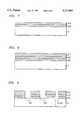
- Module 20comprises two substrates denoted by reference numerals 11 and 19.
- substrates 11 and 19are formed from single crystal silicon.
- Substrate 11, often termed the "channel plate”contains plurality of v-shaped grooves, two of which are denoted by reference numerals 13 and 15.
- substrate 11also contains a plurality of channels, one of which is denoted by reference numeral 17. Channels 17 (which may have sloping sides) extend completely through substrate 11.
- Substrate 19contains a plurality of heating elements, two of which are denoted by reference numerals 21 and 23.
- Substrate 19is termed "heater plate.”
- heating elements 21 and 23may comprise an upper layer of metal such as, tantalum overlying a layer of silicon nitride and a layer of polysilicon. The polysilicon is heated by the passage of current, thereby causing heating of the upper layer of metal).
- Heating elements 21 and 23are surrounded and partially covered by an insulating layer 24, typically polyimide. Insulator 24 defines small cavities 25 and 26 above heating elements 21 and 23 respectively.
- Substrates 11 and 19are mated together. V-groove 15 together with small cavity 25, together thereby define a passageway for ink.
- v-groove 13, together with cavity 26also thereby defines another passageway for ink.
- Energization of heating elements 21 and 23causes heating of the ink, thereby causing the ink to flow.
- Channel 17extends through substrate 11, thereby providing a conduit for an ink reservoir (not shown) and also provides a connection to v-grooves 15 and 13 (although not explicitly shown in the figure).
- reference numeral 111denotes a substrate which may be silicon, doped silicon, epitaxial silicon, etc.
- Reference numeral 131denotes a patterned oxide, typically, a thermal oxide.
- Reference numeral 132denotes a blanket layer of silicon nitride typically formed by a plasma enhanced CVD (chemical vapor deposition) process, or a low pressure CVD process. Nitride layer 132 is patterned to produce opening 133.
- An etching processtypically, a KOH etching process is performed to create channel 117.
- nitride layer 132(not shown in FIG. 3) is stripped and wafer 111 is subjected to a second chemical etch in KOH.
- the KOH etchtends to produce v-shaped grooves 113 and 115 (because, as is known to those skilled in the art, the KOH etchant tends to attack silicon planes with a orientation, and stop on planes with a 111! orientation).
- the KOH etchanttends to also attack patterned oxide 131. Consequently, the initially defined edge, 134, of oxide 131 is etched back to a subsequent position denoted by reference numeral 135. Consequently, the initially-defined v-groove 1151 becomes larger, as denoted by reference numeral 1152.
- FIG. 1depicts a conventional ink jet module.
- FIGS. 2 and 3depict a conventional method of forming v-grooves or channels in silicon substrates.
- FIG. 4depicts the conventional method of forming v-grooves in which the etchant attacks the patterned oxide.
- FIG. 5depicts a first embodiment of the present invention with a patterned thermal silicon nitride layer.
- FIGS. 6 and 7depict an alternative embodiment of the present invention in which a silicon dioxide layer and a thermal silicon nitride layer are formed on the substrate.
- FIG. 8depicts an alternative embodiment with an overlying layer for scratch protection.
- FIG. 9depicts an alternative embodiment in which patterned overlying, silicon dioxide, and thermal silicon nitride layers are used in the formation of v-grooves or channels in the substrate.
- reference numeral 11denotes a substrate which is typically, silicon, epitaxial silicon, or doped silicon. Typically, 11 is a portion of a wafer similar to wafers used to fabricate integrated circuits.
- Reference numeral 141denotes a patterned silicon nitride layer. Layer 141 is formed by a thermal nitridation process. In the thermal nitridation process, wafer 11 is exposed to an ammonia ambient, alternatively, a nitrogen ambient, (or a combination of both ammonia and nitrogen) at a temperature between 900° C. and 1200° C. at atmospheric pressure.
- the thermal nitridation processproduces a layer of silicon nitride which is in direct and intimate contact with the silicon substrate 11, i.e., there is no intermediate layer of oxide between layer 141 and substrate 11.
- Other processes for forming silicon nitridesuch as plasma enhanced chemical wafer deposition (PECVD) or low pressure chemical vapor deposition (LPCVD) are not as suitable for forming silicon nitride layer 141 because the presence of residual oxygen in the reaction chamber permits the formation of an intermediate, but thin, layer of oxide between layer 141 and substrate 11.
- PECVDplasma enhanced chemical wafer deposition
- LPCVDlow pressure chemical vapor deposition
- the thermal nitridation process described abovedisplaces oxygen which may be present at the interface between layer 141 and substrate 11.
- the thermal nitridation processmay be performed on wafers which may have a pre-existing oxide layer.
- the thickness of the wafermay be approximately 20 mils or 500 ⁇ m.
- the thickness of nitride layer 141may be 50 ⁇ .
- the width, w, of a typical v-groove 15, 13may be 25-60 ⁇ m.
- reference numeral 11denotes a silicon substrate, similar to substrate as described.
- Reference numeral 213denotes a silicon dioxide layer, having a thickness of approximately 7500 ⁇ .
- Layer 213is formed by oxidation of substrate 11 in an atmosphere of oxygen and hydrochloric acid or an atmosphere of steam at approximately 1050° C. The presence of oxide layer 213 tends to seal the edges of the wafer.
- a thermal nitridation processis performed by exposing substrate 11 to a mixture of 20% NH 3 and 80% N 2 at 1100° C. and atmospheric pressure.
- the thermal nitridation processproduces a layer of silicon nitride 215 between silicon dioxide layer 213 and substrate 11.
- the previously-formed silicon dioxide layer 213is displaced by the newly-formed silicon nitride layer 215.
- an overlying layer 217 of either LPCVD silicon nitride or polysiliconis formed for scratch protection.
- layers 217, 213, and 215are patterned (by deposition of a photoresist, exposure of the photoresist, removal of the unwanted portions of the photoresist, a plasma etch, and stripping of the resist). Then a KOH etch is performed for 3.5 hours at 95° C. to form channel 219 and v-grooves 223 and 221. Finally, layers 217, 213, and 215 are removed in a 1:1 HF--H 2 O acid bath.
- the inventive processis illustratively practiced with semiconductor wafers, such as those used for integrated circuit manufacture.
- a plurality of channel platesare formed upon a single wafer. Then the wafer is sawed, and individual channel plates are obtained for eventual combination with heater plates.
- the present processmay also find use in the formation of v-grooves or trenches which may be utilized for semiconductor device isolation in the formation of integrated circuits.
- the v-groovemay be formed as previously described.
- the groovemay be filled with LPCVD oxide which is formed, for example from TEOS.
- the groovemay be subjected to an oxidizing ambient to grow an oxide within the v-groove.
Landscapes
- Engineering & Computer Science (AREA)
- Manufacturing & Machinery (AREA)
- Physics & Mathematics (AREA)
- Condensed Matter Physics & Semiconductors (AREA)
- General Physics & Mathematics (AREA)
- Computer Hardware Design (AREA)
- Microelectronics & Electronic Packaging (AREA)
- Power Engineering (AREA)
- Element Separation (AREA)
- Weting (AREA)
- Local Oxidation Of Silicon (AREA)
- Ink Jet (AREA)
Abstract
Description
Claims (8)
Priority Applications (4)
| Application Number | Priority Date | Filing Date | Title |
|---|---|---|---|
| US08/531,115US5711891A (en) | 1995-09-20 | 1995-09-20 | Wafer processing using thermal nitride etch mask |
| EP96306564AEP0764977A2 (en) | 1995-09-20 | 1996-09-10 | Method of forming v-shaped grooves in a substrate |
| KR1019960039216AKR970018137A (en) | 1995-09-20 | 1996-09-11 | Wafer processing method |
| JP8242816AJPH09129593A (en) | 1995-09-20 | 1996-09-13 | Wafer processing method |
Applications Claiming Priority (1)
| Application Number | Priority Date | Filing Date | Title |
|---|---|---|---|
| US08/531,115US5711891A (en) | 1995-09-20 | 1995-09-20 | Wafer processing using thermal nitride etch mask |
Publications (1)
| Publication Number | Publication Date |
|---|---|
| US5711891Atrue US5711891A (en) | 1998-01-27 |
Family
ID=24116299
Family Applications (1)
| Application Number | Title | Priority Date | Filing Date |
|---|---|---|---|
| US08/531,115Expired - LifetimeUS5711891A (en) | 1995-09-20 | 1995-09-20 | Wafer processing using thermal nitride etch mask |
Country Status (4)
| Country | Link |
|---|---|
| US (1) | US5711891A (en) |
| EP (1) | EP0764977A2 (en) |
| JP (1) | JPH09129593A (en) |
| KR (1) | KR970018137A (en) |
Cited By (7)
| Publication number | Priority date | Publication date | Assignee | Title |
|---|---|---|---|---|
| US5980762A (en)* | 1996-09-02 | 1999-11-09 | Mitsubishi Denki Kabushiki Kaisha | Method of micromachining a semiconductor |
| US6310641B1 (en) | 1999-06-11 | 2001-10-30 | Lexmark International, Inc. | Integrated nozzle plate for an inkjet print head formed using a photolithographic method |
| US20040006263A1 (en)* | 2002-06-03 | 2004-01-08 | Anderson Edward J. | Noninvasive detection of a physiologic parameter within a body tissue of a patient |
| US6723250B1 (en)* | 1998-01-28 | 2004-04-20 | Robert Bosch Gmbh | Method of producing structured wafers |
| US20050118777A1 (en)* | 2003-10-31 | 2005-06-02 | Henry Bernhardt | Trench capacitor structure and process for applying a covering layer and a mask for trench etching processes in semiconductor substrates |
| US20100126961A1 (en)* | 2007-04-26 | 2010-05-27 | Sang In Kim | Polysilicon Planarization Solution for Planarizing Low Temperature Poly-Silicon Thin Film Panels |
| DE102004024105B4 (en)* | 2003-10-31 | 2011-02-10 | Qimonda Ag | Method for introducing a trench into a semiconductor substrate and for applying a cover layer |
Families Citing this family (23)
| Publication number | Priority date | Publication date | Assignee | Title |
|---|---|---|---|---|
| AUPP654598A0 (en) | 1998-10-16 | 1998-11-05 | Silverbrook Research Pty Ltd | Micromechanical device and method (ij46h) |
| AUPP654398A0 (en) | 1998-10-16 | 1998-11-05 | Silverbrook Research Pty Ltd | Micromechanical device and method (ij46g) |
| AUPP653998A0 (en) | 1998-10-16 | 1998-11-05 | Silverbrook Research Pty Ltd | Micromechanical device and method (ij46B) |
| US6742873B1 (en) | 2001-04-16 | 2004-06-01 | Silverbrook Research Pty Ltd | Inkjet printhead construction |
| US7815291B2 (en) | 1998-10-16 | 2010-10-19 | Silverbrook Research Pty Ltd | Printhead integrated circuit with low drive transistor to nozzle area ratio |
| EP1121249B1 (en) | 1998-10-16 | 2007-07-25 | Silverbrook Research Pty. Limited | Process of forming a nozzle for an inkjet printhead |
| US7216956B2 (en) | 1998-10-16 | 2007-05-15 | Silverbrook Research Pty Ltd | Printhead assembly with power and ground connections along single edge |
| US7028474B2 (en) | 1998-10-16 | 2006-04-18 | Silverbook Research Pty Ltd | Micro-electromechanical actuator with control logic circuitry |
| US7384131B2 (en) | 1998-10-16 | 2008-06-10 | Silverbrook Research Pty Ltd | Pagewidth printhead having small print zone |
| US6918655B2 (en) | 1998-10-16 | 2005-07-19 | Silverbrook Research Pty Ltd | Ink jet printhead with nozzles |
| US7419250B2 (en) | 1999-10-15 | 2008-09-02 | Silverbrook Research Pty Ltd | Micro-electromechanical liquid ejection device |
| US6863378B2 (en) | 1998-10-16 | 2005-03-08 | Silverbrook Research Pty Ltd | Inkjet printer having enclosed actuators |
| US7677686B2 (en) | 1998-10-16 | 2010-03-16 | Silverbrook Research Pty Ltd | High nozzle density printhead ejecting low drop volumes |
| US6994424B2 (en) | 1998-10-16 | 2006-02-07 | Silverbrook Research Pty Ltd | Printhead assembly incorporating an array of printhead chips on an ink distribution structure |
| US20040263551A1 (en) | 1998-10-16 | 2004-12-30 | Kia Silverbrook | Method and apparatus for firing ink from a plurality of nozzles on a printhead |
| US7111924B2 (en) | 1998-10-16 | 2006-09-26 | Silverbrook Research Pty Ltd | Inkjet printhead having thermal bend actuator heating element electrically isolated from nozzle chamber ink |
| US7182431B2 (en) | 1999-10-19 | 2007-02-27 | Silverbrook Research Pty Ltd | Nozzle arrangement |
| AUPP702198A0 (en) | 1998-11-09 | 1998-12-03 | Silverbrook Research Pty Ltd | Image creation method and apparatus (ART79) |
| US6676250B1 (en) | 2000-06-30 | 2004-01-13 | Silverbrook Research Pty Ltd | Ink supply assembly for a print engine |
| US7757574B2 (en) | 2002-01-24 | 2010-07-20 | Kla-Tencor Corporation | Process condition sensing wafer and data analysis system |
| US6889568B2 (en) | 2002-01-24 | 2005-05-10 | Sensarray Corporation | Process condition sensing wafer and data analysis system |
| US8604361B2 (en) | 2005-12-13 | 2013-12-10 | Kla-Tencor Corporation | Component package for maintaining safe operating temperature of components |
| US8681493B2 (en) | 2011-05-10 | 2014-03-25 | Kla-Tencor Corporation | Heat shield module for substrate-like metrology device |
Citations (12)
| Publication number | Priority date | Publication date | Assignee | Title |
|---|---|---|---|---|
| US4266985A (en)* | 1979-05-18 | 1981-05-12 | Fujitsu Limited | Process for producing a semiconductor device including an ion implantation step in combination with direct thermal nitridation of the silicon substrate |
| US4277320A (en)* | 1979-10-01 | 1981-07-07 | Rockwell International Corporation | Process for direct thermal nitridation of silicon semiconductor devices |
| US4298629A (en)* | 1979-03-09 | 1981-11-03 | Fujitsu Limited | Method for forming a nitride insulating film on a silicon semiconductor substrate surface by direct nitridation |
| JPS61279689A (en)* | 1985-06-05 | 1986-12-10 | Nec Corp | Structure of etching mask having protective film for side wall and its production |
| JPS63253671A (en)* | 1987-04-10 | 1988-10-20 | Nec Corp | Manufacture of semiconductor device |
| US4957592A (en)* | 1989-12-27 | 1990-09-18 | Xerox Corporation | Method of using erodable masks to produce partially etched structures in ODE wafer structures |
| US5068006A (en)* | 1990-09-04 | 1991-11-26 | Xerox Corporation | Thermal ink jet printhead with pre-diced nozzle face and method of fabrication therefor |
| EP0525650A2 (en)* | 1991-07-29 | 1993-02-03 | Nec Corporation | Semiconductor device with capacitor insulating film and method for fabricating the same |
| US5201987A (en)* | 1990-06-04 | 1993-04-13 | Xerox Corporation | Fabricating method for silicon structures |
| US5308442A (en)* | 1993-01-25 | 1994-05-03 | Hewlett-Packard Company | Anisotropically etched ink fill slots in silicon |
| US5385635A (en)* | 1993-11-01 | 1995-01-31 | Xerox Corporation | Process for fabricating silicon channel structures with variable cross-sectional areas |
| US5518946A (en)* | 1991-10-07 | 1996-05-21 | Sony Corporation | Process for fabricating capacitors in dynamic RAM |
- 1995
- 1995-09-20USUS08/531,115patent/US5711891A/ennot_activeExpired - Lifetime
- 1996
- 1996-09-10EPEP96306564Apatent/EP0764977A2/ennot_activeWithdrawn
- 1996-09-11KRKR1019960039216Apatent/KR970018137A/ennot_activeWithdrawn
- 1996-09-13JPJP8242816Apatent/JPH09129593A/enactivePending
Patent Citations (12)
| Publication number | Priority date | Publication date | Assignee | Title |
|---|---|---|---|---|
| US4298629A (en)* | 1979-03-09 | 1981-11-03 | Fujitsu Limited | Method for forming a nitride insulating film on a silicon semiconductor substrate surface by direct nitridation |
| US4266985A (en)* | 1979-05-18 | 1981-05-12 | Fujitsu Limited | Process for producing a semiconductor device including an ion implantation step in combination with direct thermal nitridation of the silicon substrate |
| US4277320A (en)* | 1979-10-01 | 1981-07-07 | Rockwell International Corporation | Process for direct thermal nitridation of silicon semiconductor devices |
| JPS61279689A (en)* | 1985-06-05 | 1986-12-10 | Nec Corp | Structure of etching mask having protective film for side wall and its production |
| JPS63253671A (en)* | 1987-04-10 | 1988-10-20 | Nec Corp | Manufacture of semiconductor device |
| US4957592A (en)* | 1989-12-27 | 1990-09-18 | Xerox Corporation | Method of using erodable masks to produce partially etched structures in ODE wafer structures |
| US5201987A (en)* | 1990-06-04 | 1993-04-13 | Xerox Corporation | Fabricating method for silicon structures |
| US5068006A (en)* | 1990-09-04 | 1991-11-26 | Xerox Corporation | Thermal ink jet printhead with pre-diced nozzle face and method of fabrication therefor |
| EP0525650A2 (en)* | 1991-07-29 | 1993-02-03 | Nec Corporation | Semiconductor device with capacitor insulating film and method for fabricating the same |
| US5518946A (en)* | 1991-10-07 | 1996-05-21 | Sony Corporation | Process for fabricating capacitors in dynamic RAM |
| US5308442A (en)* | 1993-01-25 | 1994-05-03 | Hewlett-Packard Company | Anisotropically etched ink fill slots in silicon |
| US5385635A (en)* | 1993-11-01 | 1995-01-31 | Xerox Corporation | Process for fabricating silicon channel structures with variable cross-sectional areas |
Non-Patent Citations (4)
| Title |
|---|
| Habraken et al. "Characterization of low-pressure chemical vapor deposited and thermally grown silicon nitride films" J. Appl Phys. 53 (1) pp. 404-415. |
| Habraken et al. Characterization of low pressure chemical vapor deposited and thermally grown silicon nitride films J. Appl Phys. 53 (1) pp. 404 415.* |
| Moslehi et al. "Electrical characteristics of devices fabricated with ultrathin thermally grown silicon nitride and nitroxide" 1983 Sumposium on VLSI technology. Dig. of Technical Papers, pp. 92-93. |
| Moslehi et al. Electrical characteristics of devices fabricated with ultrathin thermally grown silicon nitride and nitroxide 1983 Sumposium on VLSI technology. Dig. of Technical Papers, pp. 92 93.* |
Cited By (11)
| Publication number | Priority date | Publication date | Assignee | Title |
|---|---|---|---|---|
| US5980762A (en)* | 1996-09-02 | 1999-11-09 | Mitsubishi Denki Kabushiki Kaisha | Method of micromachining a semiconductor |
| US6723250B1 (en)* | 1998-01-28 | 2004-04-20 | Robert Bosch Gmbh | Method of producing structured wafers |
| US6310641B1 (en) | 1999-06-11 | 2001-10-30 | Lexmark International, Inc. | Integrated nozzle plate for an inkjet print head formed using a photolithographic method |
| US20040006263A1 (en)* | 2002-06-03 | 2004-01-08 | Anderson Edward J. | Noninvasive detection of a physiologic parameter within a body tissue of a patient |
| US20060020179A1 (en)* | 2002-06-03 | 2006-01-26 | Optical Sensors, Inc. | Noninvasive detection of a physiologic parameter with a probe |
| US20110152646A1 (en)* | 2002-06-03 | 2011-06-23 | Vasamed Inc. | Noninvasive detection of a physiologic parameter with a probe |
| US8996090B2 (en)* | 2002-06-03 | 2015-03-31 | Exostat Medical, Inc. | Noninvasive detection of a physiologic parameter within a body tissue of a patient |
| US20050118777A1 (en)* | 2003-10-31 | 2005-06-02 | Henry Bernhardt | Trench capacitor structure and process for applying a covering layer and a mask for trench etching processes in semiconductor substrates |
| US7547646B2 (en)* | 2003-10-31 | 2009-06-16 | Infineon Technologies Ag | Trench capacitor structure and process for applying a covering layer and a mask for trench etching processes in semiconductor substrates |
| DE102004024105B4 (en)* | 2003-10-31 | 2011-02-10 | Qimonda Ag | Method for introducing a trench into a semiconductor substrate and for applying a cover layer |
| US20100126961A1 (en)* | 2007-04-26 | 2010-05-27 | Sang In Kim | Polysilicon Planarization Solution for Planarizing Low Temperature Poly-Silicon Thin Film Panels |
Also Published As
| Publication number | Publication date |
|---|---|
| JPH09129593A (en) | 1997-05-16 |
| EP0764977A2 (en) | 1997-03-26 |
| KR970018137A (en) | 1997-04-30 |
Similar Documents
| Publication | Publication Date | Title |
|---|---|---|
| US5711891A (en) | Wafer processing using thermal nitride etch mask | |
| US4333965A (en) | Method of making integrated circuits | |
| US4363868A (en) | Process of producing semiconductor devices by forming a silicon oxynitride layer by a plasma CVD technique which is employed in a selective oxidation process | |
| US4292156A (en) | Method of manufacturing semiconductor devices | |
| US4971923A (en) | Method of making semiconductor device with different oxide film thicknesses | |
| US3986896A (en) | Method of manufacturing semiconductor devices | |
| EP0599318A2 (en) | Method for manufacturing semiconductor device having groove-structured isolation | |
| EP0050973B1 (en) | Masking process for semiconductor devices using a polymer film | |
| US6524910B1 (en) | Method of forming dual thickness gate dielectric structures via use of silicon nitride layers | |
| JPH07161806A (en) | Manufacture of semiconductor device | |
| EP0362571A2 (en) | Method for forming semiconductor components | |
| US5977608A (en) | Modified poly-buffered isolation | |
| US20040171261A1 (en) | Method of etching a silicon nitride film and method of manufacturing a semiconductor device using the same | |
| US5994216A (en) | Method of forming a reduced size contact in a dielectric layer by using bird's beak of oxidized polysilicon to create an etching mask | |
| KR100248142B1 (en) | Method of fabricating semiconductor device | |
| KR100253268B1 (en) | Semiconductor Device Insulation Method | |
| KR100306374B1 (en) | Method for forming contact hole in semiconductor device | |
| US7205243B2 (en) | Process for producing a mask on a substrate | |
| KR20010058959A (en) | Method for manufacturing semiconductor device | |
| JP2766000B2 (en) | Method for manufacturing semiconductor device | |
| JP2725616B2 (en) | Method for manufacturing semiconductor device | |
| JPH0685266A (en) | Manufacture of power mos-fet | |
| KR940009578B1 (en) | Semiconductor device and manufacturing method thereof | |
| KR100223869B1 (en) | Manufacturing method of semiconductor device | |
| KR960010461B1 (en) | Field oxide film formation method of semiconductor device |
Legal Events
| Date | Code | Title | Description |
|---|---|---|---|
| AS | Assignment | Owner name:AT&T CORP., NEW YORK Free format text:ASSIGNMENT OF ASSIGNORS INTEREST;ASSIGNOR:PEARCE, CHARLES WALTER;REEL/FRAME:007700/0160 Effective date:19950920 | |
| FEPP | Fee payment procedure | Free format text:PAYOR NUMBER ASSIGNED (ORIGINAL EVENT CODE: ASPN); ENTITY STATUS OF PATENT OWNER: LARGE ENTITY | |
| STCF | Information on status: patent grant | Free format text:PATENTED CASE | |
| FPAY | Fee payment | Year of fee payment:4 | |
| FPAY | Fee payment | Year of fee payment:8 | |
| FPAY | Fee payment | Year of fee payment:12 | |
| AS | Assignment | Owner name:DEUTSCHE BANK AG NEW YORK BRANCH, AS COLLATERAL AG Free format text:PATENT SECURITY AGREEMENT;ASSIGNORS:LSI CORPORATION;AGERE SYSTEMS LLC;REEL/FRAME:032856/0031 Effective date:20140506 | |
| AS | Assignment | Owner name:AVAGO TECHNOLOGIES GENERAL IP (SINGAPORE) PTE. LTD Free format text:ASSIGNMENT OF ASSIGNORS INTEREST;ASSIGNOR:AGERE SYSTEMS LLC;REEL/FRAME:035365/0634 Effective date:20140804 | |
| AS | Assignment | Owner name:AGERE SYSTEMS LLC, PENNSYLVANIA Free format text:TERMINATION AND RELEASE OF SECURITY INTEREST IN PATENT RIGHTS (RELEASES RF 032856-0031);ASSIGNOR:DEUTSCHE BANK AG NEW YORK BRANCH, AS COLLATERAL AGENT;REEL/FRAME:037684/0039 Effective date:20160201 Owner name:LSI CORPORATION, CALIFORNIA Free format text:TERMINATION AND RELEASE OF SECURITY INTEREST IN PATENT RIGHTS (RELEASES RF 032856-0031);ASSIGNOR:DEUTSCHE BANK AG NEW YORK BRANCH, AS COLLATERAL AGENT;REEL/FRAME:037684/0039 Effective date:20160201 | |
| AS | Assignment | Owner name:BELL SEMICONDUCTOR, LLC, ILLINOIS Free format text:ASSIGNMENT OF ASSIGNORS INTEREST;ASSIGNORS:AVAGO TECHNOLOGIES GENERAL IP (SINGAPORE) PTE. LTD.;BROADCOM CORPORATION;REEL/FRAME:044886/0608 Effective date:20171208 | |
| AS | Assignment | Owner name:CORTLAND CAPITAL MARKET SERVICES LLC, AS COLLATERA Free format text:SECURITY INTEREST;ASSIGNORS:HILCO PATENT ACQUISITION 56, LLC;BELL SEMICONDUCTOR, LLC;BELL NORTHERN RESEARCH, LLC;REEL/FRAME:045216/0020 Effective date:20180124 | |
| AS | Assignment | Owner name:BELL NORTHERN RESEARCH, LLC, ILLINOIS Free format text:RELEASE BY SECURED PARTY;ASSIGNOR:CORTLAND CAPITAL MARKET SERVICES LLC;REEL/FRAME:059720/0719 Effective date:20220401 Owner name:BELL SEMICONDUCTOR, LLC, ILLINOIS Free format text:RELEASE BY SECURED PARTY;ASSIGNOR:CORTLAND CAPITAL MARKET SERVICES LLC;REEL/FRAME:059720/0719 Effective date:20220401 Owner name:HILCO PATENT ACQUISITION 56, LLC, ILLINOIS Free format text:RELEASE BY SECURED PARTY;ASSIGNOR:CORTLAND CAPITAL MARKET SERVICES LLC;REEL/FRAME:059720/0719 Effective date:20220401 |