US5710054A - Method of forming a shallow junction by diffusion from a silicon-based spacer - Google Patents
Method of forming a shallow junction by diffusion from a silicon-based spacerDownload PDFInfo
- Publication number
- US5710054A US5710054AUS08/703,273US70327396AUS5710054AUS 5710054 AUS5710054 AUS 5710054AUS 70327396 AUS70327396 AUS 70327396AUS 5710054 AUS5710054 AUS 5710054A
- Authority
- US
- United States
- Prior art keywords
- substrate
- spacer
- gate electrode
- forming
- insulator
- Prior art date
- Legal status (The legal status is an assumption and is not a legal conclusion. Google has not performed a legal analysis and makes no representation as to the accuracy of the status listed.)
- Expired - Lifetime
Links
- 125000006850spacer groupChemical group0.000titleclaimsabstractdescription236
- 238000000034methodMethods0.000titleclaimsabstractdescription90
- XUIMIQQOPSSXEZ-UHFFFAOYSA-NSiliconChemical compound[Si]XUIMIQQOPSSXEZ-UHFFFAOYSA-N0.000titleclaimsabstractdescription43
- 229910052710siliconInorganic materials0.000titleclaimsabstractdescription43
- 239000010703siliconSubstances0.000titleclaimsabstractdescription43
- 238000009792diffusion processMethods0.000titledescription13
- 239000000758substrateSubstances0.000claimsabstractdescription227
- 239000012212insulatorSubstances0.000claimsabstractdescription128
- 239000002019doping agentSubstances0.000claimsabstractdescription88
- 239000004065semiconductorSubstances0.000claimsabstractdescription25
- 229910021420polycrystalline siliconInorganic materials0.000claimsdescription112
- 229920005591polysiliconPolymers0.000claimsdescription110
- ZOXJGFHDIHLPTG-UHFFFAOYSA-NBoronChemical compound[B]ZOXJGFHDIHLPTG-UHFFFAOYSA-N0.000claimsdescription22
- 229910052796boronInorganic materials0.000claimsdescription19
- RQNWIZPPADIBDY-UHFFFAOYSA-Narsenic atomChemical compound[As]RQNWIZPPADIBDY-UHFFFAOYSA-N0.000claimsdescription15
- VYPSYNLAJGMNEJ-UHFFFAOYSA-NSilicium dioxideChemical groupO=[Si]=OVYPSYNLAJGMNEJ-UHFFFAOYSA-N0.000claimsdescription14
- 239000007943implantSubstances0.000claimsdescription14
- 229910052785arsenicInorganic materials0.000claimsdescription11
- 239000002210silicon-based materialSubstances0.000claimsdescription9
- 238000005530etchingMethods0.000claimsdescription7
- 229910052698phosphorusInorganic materials0.000claimsdescription7
- 239000000377silicon dioxideSubstances0.000claimsdescription7
- 238000000151depositionMethods0.000claimsdescription6
- 238000009826distributionMethods0.000claimsdescription6
- OAICVXFJPJFONN-UHFFFAOYSA-NPhosphorusChemical compound[P]OAICVXFJPJFONN-UHFFFAOYSA-N0.000claimsdescription5
- 239000011574phosphorusSubstances0.000claimsdescription5
- 238000004519manufacturing processMethods0.000claimsdescription4
- 235000012239silicon dioxideNutrition0.000claimsdescription4
- 229910052581Si3N4Inorganic materials0.000claimsdescription3
- HQVNEWCFYHHQES-UHFFFAOYSA-Nsilicon nitrideChemical compoundN12[Si]34N5[Si]62N3[Si]51N64HQVNEWCFYHHQES-UHFFFAOYSA-N0.000claimsdescription3
- 229910021417amorphous siliconInorganic materials0.000claimsdescription2
- 239000010410layerSubstances0.000description18
- 238000005468ion implantationMethods0.000description10
- 239000000463materialSubstances0.000description7
- 230000005465channelingEffects0.000description5
- 239000007772electrode materialSubstances0.000description5
- 238000012545processingMethods0.000description5
- 230000008901benefitEffects0.000description4
- 230000000694effectsEffects0.000description4
- 230000005684electric fieldEffects0.000description4
- 230000015572biosynthetic processEffects0.000description3
- 229910052681coesiteInorganic materials0.000description3
- 229910052906cristobaliteInorganic materials0.000description3
- 230000005669field effectEffects0.000description3
- 238000002513implantationMethods0.000description3
- 229910052757nitrogenInorganic materials0.000description3
- 229920002120photoresistant polymerPolymers0.000description3
- 229910052682stishoviteInorganic materials0.000description3
- 229910052905tridymiteInorganic materials0.000description3
- IJGRMHOSHXDMSA-UHFFFAOYSA-NAtomic nitrogenChemical compoundN#NIJGRMHOSHXDMSA-UHFFFAOYSA-N0.000description2
- 230000004888barrier functionEffects0.000description2
- 239000000969carrierSubstances0.000description2
- 239000003989dielectric materialSubstances0.000description2
- 238000006073displacement reactionMethods0.000description2
- 238000010884ion-beam techniqueMethods0.000description2
- 150000002500ionsChemical class0.000description2
- 238000004518low pressure chemical vapour depositionMethods0.000description2
- 238000012986modificationMethods0.000description2
- 230000004048modificationEffects0.000description2
- 230000003647oxidationEffects0.000description2
- 238000007254oxidation reactionMethods0.000description2
- 238000000206photolithographyMethods0.000description2
- 230000008569processEffects0.000description2
- 230000000979retarding effectEffects0.000description2
- 239000000126substanceSubstances0.000description2
- 239000002344surface layerSubstances0.000description2
- RTAQQCXQSZGOHL-UHFFFAOYSA-NTitaniumChemical compound[Ti]RTAQQCXQSZGOHL-UHFFFAOYSA-N0.000description1
- 230000004913activationEffects0.000description1
- 230000002411adverseEffects0.000description1
- 229910052782aluminiumInorganic materials0.000description1
- XAGFODPZIPBFFR-UHFFFAOYSA-NaluminiumChemical compound[Al]XAGFODPZIPBFFR-UHFFFAOYSA-N0.000description1
- 230000003466anti-cipated effectEffects0.000description1
- 238000013459approachMethods0.000description1
- 230000008859changeEffects0.000description1
- 239000004020conductorSubstances0.000description1
- 238000007796conventional methodMethods0.000description1
- 239000013078crystalSubstances0.000description1
- 230000003247decreasing effectEffects0.000description1
- 230000008021depositionEffects0.000description1
- 230000002708enhancing effectEffects0.000description1
- 230000006870functionEffects0.000description1
- 239000002784hot electronSubstances0.000description1
- 238000005304joiningMethods0.000description1
- 230000008018meltingEffects0.000description1
- 238000002844meltingMethods0.000description1
- QSHDDOUJBYECFT-UHFFFAOYSA-NmercuryChemical compound[Hg]QSHDDOUJBYECFT-UHFFFAOYSA-N0.000description1
- 229910052751metalInorganic materials0.000description1
- 239000002184metalSubstances0.000description1
- 229910044991metal oxideInorganic materials0.000description1
- 150000004706metal oxidesChemical class0.000description1
- 238000001465metallisationMethods0.000description1
- 229910021421monocrystalline siliconInorganic materials0.000description1
- 150000004767nitridesChemical class0.000description1
- 238000012856packingMethods0.000description1
- 230000003071parasitic effectEffects0.000description1
- 238000002161passivationMethods0.000description1
- 238000000059patterningMethods0.000description1
- 238000005381potential energyMethods0.000description1
- 238000012552reviewMethods0.000description1
- 229910021332silicideInorganic materials0.000description1
- FVBUAEGBCNSCDD-UHFFFAOYSA-Nsilicide(4-)Chemical compound[Si-4]FVBUAEGBCNSCDD-UHFFFAOYSA-N0.000description1
- 239000013589supplementSubstances0.000description1
- 239000010409thin filmSubstances0.000description1
- 239000010936titaniumSubstances0.000description1
- 229910052719titaniumInorganic materials0.000description1
Images


Classifications
- H—ELECTRICITY
- H10—SEMICONDUCTOR DEVICES; ELECTRIC SOLID-STATE DEVICES NOT OTHERWISE PROVIDED FOR
- H10D—INORGANIC ELECTRIC SEMICONDUCTOR DEVICES
- H10D62/00—Semiconductor bodies, or regions thereof, of devices having potential barriers
- H10D62/10—Shapes, relative sizes or dispositions of the regions of the semiconductor bodies; Shapes of the semiconductor bodies
- H10D62/13—Semiconductor regions connected to electrodes carrying current to be rectified, amplified or switched, e.g. source or drain regions
- H10D62/149—Source or drain regions of field-effect devices
- H10D62/151—Source or drain regions of field-effect devices of IGFETs
- H—ELECTRICITY
- H01—ELECTRIC ELEMENTS
- H01L—SEMICONDUCTOR DEVICES NOT COVERED BY CLASS H10
- H01L21/00—Processes or apparatus adapted for the manufacture or treatment of semiconductor or solid state devices or of parts thereof
- H01L21/02—Manufacture or treatment of semiconductor devices or of parts thereof
- H01L21/04—Manufacture or treatment of semiconductor devices or of parts thereof the devices having potential barriers, e.g. a PN junction, depletion layer or carrier concentration layer
- H01L21/18—Manufacture or treatment of semiconductor devices or of parts thereof the devices having potential barriers, e.g. a PN junction, depletion layer or carrier concentration layer the devices having semiconductor bodies comprising elements of Group IV of the Periodic Table or AIIIBV compounds with or without impurities, e.g. doping materials
- H01L21/22—Diffusion of impurity materials, e.g. doping materials, electrode materials, into or out of a semiconductor body, or between semiconductor regions; Interactions between two or more impurities; Redistribution of impurities
- H01L21/225—Diffusion of impurity materials, e.g. doping materials, electrode materials, into or out of a semiconductor body, or between semiconductor regions; Interactions between two or more impurities; Redistribution of impurities using diffusion into or out of a solid from or into a solid phase, e.g. a doped oxide layer
- H01L21/2251—Diffusion into or out of group IV semiconductors
- H01L21/2254—Diffusion into or out of group IV semiconductors from or through or into an applied layer, e.g. photoresist, nitrides
- H01L21/2255—Diffusion into or out of group IV semiconductors from or through or into an applied layer, e.g. photoresist, nitrides the applied layer comprising oxides only, e.g. P2O5, PSG, H3BO3, doped oxides
- H01L21/2256—Diffusion into or out of group IV semiconductors from or through or into an applied layer, e.g. photoresist, nitrides the applied layer comprising oxides only, e.g. P2O5, PSG, H3BO3, doped oxides through the applied layer
- H—ELECTRICITY
- H01—ELECTRIC ELEMENTS
- H01L—SEMICONDUCTOR DEVICES NOT COVERED BY CLASS H10
- H01L21/00—Processes or apparatus adapted for the manufacture or treatment of semiconductor or solid state devices or of parts thereof
- H01L21/02—Manufacture or treatment of semiconductor devices or of parts thereof
- H01L21/04—Manufacture or treatment of semiconductor devices or of parts thereof the devices having potential barriers, e.g. a PN junction, depletion layer or carrier concentration layer
- H01L21/18—Manufacture or treatment of semiconductor devices or of parts thereof the devices having potential barriers, e.g. a PN junction, depletion layer or carrier concentration layer the devices having semiconductor bodies comprising elements of Group IV of the Periodic Table or AIIIBV compounds with or without impurities, e.g. doping materials
- H01L21/22—Diffusion of impurity materials, e.g. doping materials, electrode materials, into or out of a semiconductor body, or between semiconductor regions; Interactions between two or more impurities; Redistribution of impurities
- H01L21/225—Diffusion of impurity materials, e.g. doping materials, electrode materials, into or out of a semiconductor body, or between semiconductor regions; Interactions between two or more impurities; Redistribution of impurities using diffusion into or out of a solid from or into a solid phase, e.g. a doped oxide layer
- H01L21/2251—Diffusion into or out of group IV semiconductors
- H01L21/2254—Diffusion into or out of group IV semiconductors from or through or into an applied layer, e.g. photoresist, nitrides
- H01L21/2257—Diffusion into or out of group IV semiconductors from or through or into an applied layer, e.g. photoresist, nitrides the applied layer being silicon or silicide or SIPOS, e.g. polysilicon, porous silicon
- H—ELECTRICITY
- H01—ELECTRIC ELEMENTS
- H01L—SEMICONDUCTOR DEVICES NOT COVERED BY CLASS H10
- H01L21/00—Processes or apparatus adapted for the manufacture or treatment of semiconductor or solid state devices or of parts thereof
- H01L21/02—Manufacture or treatment of semiconductor devices or of parts thereof
- H01L21/04—Manufacture or treatment of semiconductor devices or of parts thereof the devices having potential barriers, e.g. a PN junction, depletion layer or carrier concentration layer
- H01L21/18—Manufacture or treatment of semiconductor devices or of parts thereof the devices having potential barriers, e.g. a PN junction, depletion layer or carrier concentration layer the devices having semiconductor bodies comprising elements of Group IV of the Periodic Table or AIIIBV compounds with or without impurities, e.g. doping materials
- H01L21/28—Manufacture of electrodes on semiconductor bodies using processes or apparatus not provided for in groups H01L21/20 - H01L21/268
- H01L21/28008—Making conductor-insulator-semiconductor electrodes
- H01L21/28017—Making conductor-insulator-semiconductor electrodes the insulator being formed after the semiconductor body, the semiconductor being silicon
- H01L21/28026—Making conductor-insulator-semiconductor electrodes the insulator being formed after the semiconductor body, the semiconductor being silicon characterised by the conductor
- H01L21/28105—Making conductor-insulator-semiconductor electrodes the insulator being formed after the semiconductor body, the semiconductor being silicon characterised by the conductor the final conductor next to the insulator having a lateral composition or doping variation, or being formed laterally by more than one deposition step
- H—ELECTRICITY
- H01—ELECTRIC ELEMENTS
- H01L—SEMICONDUCTOR DEVICES NOT COVERED BY CLASS H10
- H01L21/00—Processes or apparatus adapted for the manufacture or treatment of semiconductor or solid state devices or of parts thereof
- H01L21/02—Manufacture or treatment of semiconductor devices or of parts thereof
- H01L21/04—Manufacture or treatment of semiconductor devices or of parts thereof the devices having potential barriers, e.g. a PN junction, depletion layer or carrier concentration layer
- H01L21/18—Manufacture or treatment of semiconductor devices or of parts thereof the devices having potential barriers, e.g. a PN junction, depletion layer or carrier concentration layer the devices having semiconductor bodies comprising elements of Group IV of the Periodic Table or AIIIBV compounds with or without impurities, e.g. doping materials
- H01L21/28—Manufacture of electrodes on semiconductor bodies using processes or apparatus not provided for in groups H01L21/20 - H01L21/268
- H01L21/28008—Making conductor-insulator-semiconductor electrodes
- H01L21/28017—Making conductor-insulator-semiconductor electrodes the insulator being formed after the semiconductor body, the semiconductor being silicon
- H01L21/28026—Making conductor-insulator-semiconductor electrodes the insulator being formed after the semiconductor body, the semiconductor being silicon characterised by the conductor
- H01L21/28114—Making conductor-insulator-semiconductor electrodes the insulator being formed after the semiconductor body, the semiconductor being silicon characterised by the conductor characterised by the sectional shape, e.g. T, inverted-T
- H—ELECTRICITY
- H10—SEMICONDUCTOR DEVICES; ELECTRIC SOLID-STATE DEVICES NOT OTHERWISE PROVIDED FOR
- H10D—INORGANIC ELECTRIC SEMICONDUCTOR DEVICES
- H10D30/00—Field-effect transistors [FET]
- H10D30/01—Manufacture or treatment
- H10D30/021—Manufacture or treatment of FETs having insulated gates [IGFET]
- H10D30/0223—Manufacture or treatment of FETs having insulated gates [IGFET] having source and drain regions or source and drain extensions self-aligned to sides of the gate
- H10D30/0227—Manufacture or treatment of FETs having insulated gates [IGFET] having source and drain regions or source and drain extensions self-aligned to sides of the gate having both lightly-doped source and drain extensions and source and drain regions self-aligned to the sides of the gate, e.g. lightly-doped drain [LDD] MOSFET or double-diffused drain [DDD] MOSFET
- H—ELECTRICITY
- H10—SEMICONDUCTOR DEVICES; ELECTRIC SOLID-STATE DEVICES NOT OTHERWISE PROVIDED FOR
- H10D—INORGANIC ELECTRIC SEMICONDUCTOR DEVICES
- H10D30/00—Field-effect transistors [FET]
- H10D30/60—Insulated-gate field-effect transistors [IGFET]
- H10D30/601—Insulated-gate field-effect transistors [IGFET] having lightly-doped drain or source extensions, e.g. LDD IGFETs or DDD IGFETs
- H10D30/608—Insulated-gate field-effect transistors [IGFET] having lightly-doped drain or source extensions, e.g. LDD IGFETs or DDD IGFETs having non-planar bodies, e.g. having recessed gate electrodes
- H—ELECTRICITY
- H10—SEMICONDUCTOR DEVICES; ELECTRIC SOLID-STATE DEVICES NOT OTHERWISE PROVIDED FOR
- H10D—INORGANIC ELECTRIC SEMICONDUCTOR DEVICES
- H10D62/00—Semiconductor bodies, or regions thereof, of devices having potential barriers
- H10D62/01—Manufacture or treatment
- H10D62/021—Forming source or drain recesses by etching e.g. recessing by etching and then refilling
- H—ELECTRICITY
- H10—SEMICONDUCTOR DEVICES; ELECTRIC SOLID-STATE DEVICES NOT OTHERWISE PROVIDED FOR
- H10D—INORGANIC ELECTRIC SEMICONDUCTOR DEVICES
- H10D64/00—Electrodes of devices having potential barriers
- H10D64/01—Manufacture or treatment
- H10D64/021—Manufacture or treatment using multiple gate spacer layers, e.g. bilayered sidewall spacers
- H—ELECTRICITY
- H10—SEMICONDUCTOR DEVICES; ELECTRIC SOLID-STATE DEVICES NOT OTHERWISE PROVIDED FOR
- H10D—INORGANIC ELECTRIC SEMICONDUCTOR DEVICES
- H10D64/00—Electrodes of devices having potential barriers
- H10D64/20—Electrodes characterised by their shapes, relative sizes or dispositions
- H10D64/23—Electrodes carrying the current to be rectified, amplified, oscillated or switched, e.g. sources, drains, anodes or cathodes
- H10D64/251—Source or drain electrodes for field-effect devices
- H10D64/258—Source or drain electrodes for field-effect devices characterised by the relative positions of the source or drain electrodes with respect to the gate electrode
- H10D64/259—Source or drain electrodes being self-aligned with the gate electrode and having bottom surfaces higher than the interface between the channel and the gate dielectric
Definitions
- the present inventionrelates to integrated circuit manufacturing, and more particularly to method of forming a junction for an insulated-gate field-effect transistor.
- An insulated-gate field-effect transistorsuch as a metal-oxide semiconductor field-effect transistor (MOSFET) uses a gate electrode to control an underlying surface channel joining a source and a drain.
- the channel, source and drainare located in a semiconductor substrate, with the substrate being doped oppositely to the source and drain.
- the gate electrodeis separated from the semiconductor substrate by a thin insulating layer such as a gate oxide.
- the operation of the IGFETinvolves application of an input voltage to the gate electrode, which sets up a transverse electric field in the channel in order to modulate the longitudinal conductance of the channel.
- the source and drainare formed by introducing dopants of a second conductivity type (P or N) into the semiconductor substrate of a first conductivity type (N or P) using a patterned gate electrode as a mask.
- This self-aligning proceduretends to improve packing density and reduce parasitic overlap capacitances between the gate electrode and the source/drain regions.
- Polysiliconalso called polycrystalline silicon, poly-Si or poly
- thin filmshave many important uses in IGFET technology.
- One of the key innovationsis the use of heavily doped polysilicon as the gate electrode in place of aluminum. Since polysilicon has the same high melting point as a silicon substrate, it can be deposited prior to source and drain formation, and serve as a mask during formation of the source and drain regions by ion implantation. The resistance of polysilicon can be further reduced by forming a silicide on its top surface.
- the electric field in the channel near the draintends to increase. If the electric field becomes strong enough, it can give rise to so-called hot-carrier effects. For instance, hot electrons can overcome the potential energy barrier between the substrate and the gate insulator thereby causing hot carriers to become injected into the gate insulator. Trapped charge in the gate insulator due to injected hot carriers accumulates over time and can lead to a permanent change in the threshold voltage of the device.
- LDDlightly doped drain
- the LDDreduces hot carrier effects by reducing the maximum lateral electric field.
- the drainis typically formed by two ion implants.
- a light implantis self-aligned to the gate electrode, and a heavy implant is self-aligned to the gate electrode on which sidewall spacers have been formed.
- the spacersare typically oxides or nitrides.
- the purpose of the lighter first doseis to form a lightly doped region of the drain (or LDD) at the edge near the channel.
- the second heavier doseforms a low resistivity region of the drain, which is subsequently merged with the lightly doped region. Since the heavily doped region is farther away from the channel than a conventional drain structure, the depth of the heavily doped region can be made somewhat greater without adversely affecting the device characteristics.
- a phenomena called "channeling"may occur when the ion beam which implants the dopants is closely aligned with the crystal lattice of the silicon.
- channelingoccurs, the dopants are initially implanted deeper beneath the top surface of the substrate, but then as implantation continues the substrate surface becomes amorphous and less channeling occurs.
- the depth of the channeled dopantsis difficult to control.
- Channelingcan be avoided by tilting the substrate (typically, at an angle of 7°) with respect to the ion beam.
- implanting off-axiscan cause asymmetric doping of the source and drain regions.
- Another drawback of ion implantationis random scattering of the implanted dopants.
- the random scatteringresults in a small portion of implanted regions, measured as the "lateral straggle,” being disposed beneath the mask.
- a further drawback of ion implantationis that the concentration (or doping profile) of the implanted dopants typically forms a gaussian distribution along the vertical axis in which the peak concentration is substantially below the top surface of the substrate. Furthermore, driving-in the dopants by high-temperature processing causes the implanted dopants to diffuse farther into the substrate.
- a strategy for enhancing IGFET performanceis to have the dopant atoms as close to the surface of the substrate as possible. Restricting current flow to a very narrow layer between the source and drain tends to improve current drive properties, and also reduce off-state leakage current. Accordingly, as IGFET dimensions are reduced, it is highly desirable to form shallow channel junctions on the order of 0.01 to 0.15 microns deep in order to improve transistor performance.
- LDD regions and other source/drain structuresare frequently formed using ion implantation. Even as ion implantation energies are scaled down to the range of 5 to 10 kiloelectron-volts and smaller, it remains difficult or impossible to form well-controlled shallow junctions using conventional semiconductor implantation equipment.
- the present inventionprovides an improved method of forming a shallow junction for an IGFET transistor.
- a key feature of the inventionis forming the shallow junction by diffusing a dopant from a silicon-based spacer into the substrate.
- the spaceris disposed in close lateral relationship to a gate electrode so that the shallow junction is substantially aligned with an edge of the gate electrode.
- the shallow junctionhas a depth in the range of about 0.01 to 0.15 microns.
- an object of the present inventionis provide shallow junctions which are less susceptible to the channeling, lateral diffusion, and other drawbacks associated with conventional ion implantation techniques.
- the methodincludes the steps of forming a gate insulator on a semiconductor substrate of first conductivity type, forming a gate electrode on the gate insulator, forming a sidewall insulator on the edge of the gate electrode, forming a silicon-based spacer over the substrate and adjacent to the sidewall insulator, and diffusing a dopant of second conductive type from the spacer into the substrate to form a shallow region of the second conductivity type in the substrate.
- the shallow regionforms the shallow junction.
- the silicon-based spacercan be formed directly on the substrate, or formed on a thin oxide layer on the substrate.
- the shallow regioncan be an LDD region, in which case a heavily doped region is implanted using the silicon-based spacer as a mask and then merged with the LDD region.
- the shallow regioncan provide the source or the drain.
- the spacerprovides an electrical contact to the shallow region and/or the heavily doped region.
- the sidewall insulatorcan be an oxide grown or deposited on the edge of the gate electrode.
- the spacercan be doped either before or after it is formed by an anisotropic etch.
- the gate electrode and spacercan be oppositely doped silicon-based materials disposed adjacent to one another, such that adjacent sidewalls form a PN junction. Reverse-biasing the PN junction during operation serves to electrically isolate the gate electrode and the spacer.
- the sidewall insulatorcan cover an edge of the gate insulator and extend to the substrate.
- the sidewall insulatorcan extend only to the bottom of the gate electrode so that the spacer is formed on a portion of the substrate adjacent to the gate insulator.
- the spacercan be formed on a portion of the substrate that is recessed with respect to a portion of the substrate underlying the gate electrode so that the dopant diffuses laterally through a sidewall of the substrate.
- the gate electrode and spacerare polysilicon
- the gate insulator and sidewall insulatorsare oxides
- the dopantis boron, arsenic, or phosphorus.
- An advantage of the inventionis that the diffused dopant from the silicon-based spacer is well-suited to forming shallow junctions. Another advantage is that the concentration of the diffused dopant in the shallow region typically resembles the upper-half of a gaussian distribution along the vertical axis in which the peak dopant concentration is in close proximity to the top surface of the substrate. As a result, the shallow region and junction are relatively well controlled.
- FIGS. 1A-1Fshow cross-sectional views of successive process steps for forming a shallow junction in accordance with a first embodiment of the invention
- FIGS. 2A-2Fshow cross-sectional views of successive process steps for forming a shallow junction in accordance with a second embodiment of the invention
- FIGS. 3A-3Eshow cross-sectional views of successive process steps for forming a shallow junction in accordance with a third embodiment of the invention
- FIGS. 4A-4Eshow cross-sectional views of successive process steps for forming a shallow junction in accordance with a fourth embodiment of the invention.
- FIGS. 5A-5Dshow cross-sectional views of successive process steps for forming a shallow junction in accordance with a fifth embodiment of the invention.
- FIGS. 6A-6Fshow cross-sectional views of successive process steps for forming a shallow junction in accordance with a sixth embodiment of the invention.
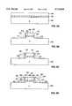
- FIGS. 1A-1Fshow cross-sectional views of successive process steps for forming a shallow junction in accordance with a first embodiment of the invention.
- a gate electrode materialis disposed on a gate insulator material, which in turn is disposed on a semiconductor substrate suitable for integrated circuit manufacture.
- substrate 102includes a P-type epitaxial surface layer with a ⁇ 100> orientation and a resistivity of 12 ohm-cm.
- the epitaxial surface layeris disposed on a P+ base layer (not shown).
- a blanket layer of gate oxide 104(such as SiO 2 ) is formed on the top surface of substrate 102 using robe growth at a temperature of 700° to 1000° C. in an O 2 containing ambient.
- Gate oxide 104has a thickness in the range of 30 to 200 angstroms.
- polysilicon 106is deposited by low pressure chemical vapor deposition on the top surface of gate oxide 104.
- Polysilicon 106has a thickness in the range of 250 to 4000 angstroms.
- Polysilicon 106is doped by ion implantation of arsenic at a dose in the range of 1 ⁇ 10 15 to 5 ⁇ 10 15 atoms/cm 2 and an energy in the range of 2 to 80 kiloelectron-volts.
- polysilicon 106can be doped by a subsequent source/drain implant.
- the gate electrode material and the gate insulator materialare patterned to provide the gate electrode and gate insulator, respectively.
- polysilicon 106 and gate oxide 104are patterned using conventional photolithography and an anisotropic etch. For submicron dimensions, patterning a photoresist mask (not shown) by I-line photolithography using a mercury vapor lamp is preferred. After the photoresist mask is patterned, an isotropic etch is applied, polysilicon 106 is etched back to provide a gate electrode, and gate oxide 104 is etched back to provide a gate insulator.
- a first etchantis applied that is highly selective of polysilicon
- a second etchantis applied that is highly selective of oxides.
- polysilicon 106includes opposing vertical edges 110 and 112, and gate oxide 104 includes opposing vertical edges 114 and 116. Edges 110 and 114 are substantially laterally aligned, and edges 112 and 116 are substantially laterally aligned.
- Polysilicon 106has a length (between edges 110 and 112) of about 0.4 to 0.5 microns. The portions of substrate 102 outside polysilicon 106 are exposed and substantially unaffected by the etch. Therefore, the top surface of substrate 102 outside polysilicon 106 is substantially vertically aligned (or coplanar) with portion 118 of substrate 102 underlying polysilicon 106.
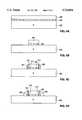
- a sidewall insulatoris formed on an edge of the gate electrode.
- a layer of oxidesuch as SiO 2
- the oxidation rate of polysiliconis greater that the oxidation rate of single crystal silicon, particularly if the polysilicon is doped with arsenic. Therefore, the oxide grown on substrate 102 can be removed using a single dip in a wet chemical etchant. Furthermore, the oxide grown on the top surface of polysilicon 106 can also be removed using conventional techniques, such as a second dip in a wet chemical etchant. As a result, thin sidewall oxides 120 and 122 cover polysilicon edges 110 and 112, respectively.
- Sidewall oxides 120 and 122each extend a lateral distance in the range of 200 to 1000 angstroms, have about the same height as polysilicon 106, and are vertically spaced from substrate 102. Portions 124 and 126 of substrate 102 beneath sidewall oxides 120 and 122, respectively, are exposed, and oxide edges 114 and 116 are exposed.
- a silicon-based spaceris formed over the substrate, such that the sidewall insulator is disposed between the gate electrode and the spacer.
- a second blanket layer of polysiliconis deposited by low pressure chemical vapor deposition over substrate 102, and the second blanket layer of polysilicon is doped by ion implantation of arsenic at a dose in the range of 1 ⁇ 10 13 to 5 ⁇ 10 14 atoms/cm 2 and an energy in the range of 2 to 80 kiloelectron-volts.
- an anisotropic etchprovided by a reactive ion etch, is applied to the second blanket layer of polysilicon to form polysilicon spacers 130 and 132.
- Spacers 130 and 132contact portions of substrate 102 including portions 124 and 126, respectively. Spacers 130 and 132 also contact gate oxide edges 114 and 116, respectively, and sidewall oxides 120 and 122, respectively. However, spacers 130 and 132 do not contact polysilicon 106. Instead, spacers 130 and 132 are laterally spaced from and electrically isolated from edges 110 and 112 of polysilicon 106 by sidewall oxides 120 and 122, respectively. The height of spacers 130 and 132 is substantially the same as the combined heights of gate oxide 104 and polysilicon 106.
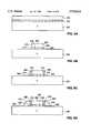
- a heavily doped regionis implanted into the substrate using the spacer as a mask.
- heavily doped N+ regions 140 and 142are formed in substrate 102 using polysilicon 106, sidewall oxides 120 and 122, and spacers 130 and 132 as an implant mask.
- the implantis performed using arsenic at a dosage of 1 ⁇ 10 15 to 5 ⁇ 10 15 atoms/cm 2 and an energy in the range of 2 to 80 kiloelectron-volts.
- heavily doped regions 140 and 142have an N+ arsenic concentration in the range of 1 ⁇ 10 18 to 1 ⁇ 10 19 atoms/cm 3 and a depth in the range of 0.02 to 0.3 microns.
- the dopant atoms in the silicon-based spacerare diffused into the substrate.
- a rapid thermal anneal on the order of 950° to 1050° C. for 10 to 30 secondsserves to drive arsenic atoms out of spacers 130 and 132.
- the arsenic atomsdiffuse from spacers 130 and 132 into substrate 102 to form shallow regions 150 and 152, respectively, which are lightly doped N- with an arsenic concentration in the range of 1 ⁇ 10 17 to 1 ⁇ 10 18 atoms/cm 3 and a depth in the range of 0.01 to 0.15 microns.
- shallow regions 150 and 152are provided by diffusion from spacers 130 and 132, respectively.
- heavily doped regions 140 and 142have a substantially greater depth than shallow regions 150 and 152.
- Shallow regions 150 and 152form shallow junctions 154 and 156, respectively, which are substantially laterally aligned with edges 110 and 112, respectively, of polysilicon 106.
- junctions 154 and 156define the channel length of an N-channel MOSFET controlled by polysilicon 106.
- Shallow regions 150 and 152are lightly doped regions due to the relatively light doping of spacers 130 and 132.
- the anneal (or drive-in) stepalso activates the implanted dopants in regions 140 and 142 and diffuses them farther into substrate 102.
- regions 140 and 150merge to form a drain (in which region 150 provides an LDD), and regions 142 and 152 merge to form a source.
- the drain and sourceare entirely within and extend to the top surface of substrate 102.
- regions 140 and 142laterally diffuse beneath spacers 130 and 132, respectively.
- spacer 130is in electfical contact with region 140 and provides a drain contact
- spacer 132is in electrical contact with region 142 and provides a source contact.
- FIGS. 2A-2Fshow cross-sectional views of successive process steps for forming a shallow junction in accordance with a second embodiment of the invention. It is often desirable to minimize the lateral overlap between the gate electrode and the source/drain, since reducing overlap capacitance improves switching speeds. However, decreasing the channel length increases drive current. Thus, the overlap between the gate electrode and source/drain involves a tradeoff between switching speed and drive current.
- the primary difference between the second embodiment and the first embodimentis that in the second embodiment, a portion of the substrate outside the gate electrode is recessed so that the spacers contact a sidewall of the substrate, dopants laterally diffuse from the spacers through the sidewall, and therefore the lateral overlap between the shallow region and the gate electrode is increased.
- the elements for the second embodimente.g., substrate 202, gate oxide 204, etc.
- the elements for the first embodimente.g., substrate 102, gate oxide 104, etc.
- the description of related elements and process stepsneed not be repeated.
- gate oxide 204is formed on substrate 202, and polysilicon 206 is formed on gate oxide 204.
- the gate electrode material and the gate insulator materialare patterned to provide the gate electrode and gate insulator, respectively.
- a substantial portion of the substrate outside the gate electrodeis partially etched back.
- polysilicon 206 and gate oxide 204are etched in a similar manner to polysilicon 106 and gate oxide 104, respectively.
- the photoresist mask(not shown) is left in place, and another etch is applied so that the portion of substrate 202 outside the remaining polysilicon 206 is partially etched back between 100 to 2000 angstroms.
- substrate 202is etched using the same etchant applied to polysilicon 206.
- polysilicon 206includes opposing vertical edges 210 and 212
- gate oxide 204includes opposing vertical edges 214 and 216
- substrate 202includes opposing vertical edges 217 and 219. Edges 210, 214 and 217 are substantially laterally aligned, as are edges 212, 216 and 219. Therefore, the top surface of substrate 202 outside polysilicon 206 is recessed with respect to portion 218 of substrate 202 underlying polysilicon 206.
- thin sidewall oxides 220 and 222are formed on polysilicon edges 210 and 212, respectively. Portions 224 and 226 of substrate 202 are located beneath sidewall oxides 220 and 222, respectively, are adjacent to substrate edges 217 and 219, respectively, and are exposed.
- spacers 230 and 232are formed on substrate 202. Spacers 230 and 232 contact edges 217 and 219, respectively, and portions 224 and 226, respectively, of substrate 202. Spacers 230 and 232 also contact gate oxide edges 214 and 216, respectively, and sidewall oxides 220 and 222, respectively. However, spacers 230 and 232 are laterally separated and electrically isolated from polysilicon 206.
- heavily doped regions 240 and 242are formed in substrate 202 using polysilicon 206, sidewall oxides 220 and 222, and spacers 230 and 232 as an implant mask.
- the dopant in the silicon-based spacersis diffused into the substrate.
- the dopantvertically diffuses through the recessed surface of the substrate.
- the dopantalso laterally diffuses through a sidewall of the substrate that is substantially laterally aligned with an edge of the gate electrode. Accordingly, the arsenic atoms vertically diffuse from spacers 230 and 232 through the recessed portion of substrate 202 including portions 224 and 226, respectively, and the arsenic atoms laterally diffuse from spacers 230 and 232 through sidewalls 217 and 219, respectively, toward the lateral center of polysilicon 206.
- Shallow regions 250 and 252form shallow junctions 254 and 256, respectively, which are substantially laterally aligned with edges 210 and 212, respectively, of polysilicon 206, although the lateral overlap is somewhat greater than that of junctions 154 and 156 with edges 110 and 112, respectively.
- Regions 250 and 252are lightly doped regions which merge with regions 240 and 242, respectively, to form a drain and source, respectively, in electrical contact with spacers 230 and 232, respectively.
- FIGS. 3A-3Eshow cross-sectional views of successive process steps for forming a shallow junction in accordance with a third embodiment of the invention.
- the present inventionis well-suited for forming P-channel MOSFETs as well as N-channel MOSFETs.
- Boronis a commonly used P-type dopant.
- borontends to diffuse much faster than typical N-type dopants such as arsenic and phosphorus, and also tends to diffuse laterally by significant amounts. Accordingly, when boron is the dopant, it may be desirable to retard the diffusion of boron to assure that the shallow regions are properly formed and well controlled.
- One method of retarding boron diffusion from the spaceris by disposing a thin barrier between the spacer and the substrate.
- the spacersare doped with boron, and the spacers are formed on a spacer insulator formed on the substrate, instead of the spacers being formed directly on the substrate.
- the elements for the third embodimente.g., substrate 302, gate oxide 304, etc.
- the elements for the third embodimentare similar to elements of the first embodiment (e.g., substrate 102, gate oxide 104, etc.), and the description of related elements and process steps need not be repeated.
- gate oxide 304is formed on substrate 302, and polysilicon 306 is formed on gate oxide 304.
- Substrate 302is similar to substrate 102, except substrate 302 is doped N-type.
- the gate electrode material and the gate insulator materialare patterned to provide the gate electrode and gate insulator, respectively, and a spacer insulator is also formed.
- a substantial portion of the gate oxide outside the gate electrodeis not removed.
- polysilicon 306is etched in a similar manner to polysilicon 106, then gate oxide 304 outside polysilicon 306 is partially etched back in the range of 20 to 150 angstroms to a thickness in the range of 10 to 50 angstroms.
- the partially etched back oxide outside polysilicon 306is referred to as spacer oxide 305.
- spacer oxide 305is used to retard (but not block) diffusion of the dopant from the silicon-based spacer into the substrate. If desired, spacer oxide 305 can be implanted with nitrogen to further retard the diffusion.
- thin sidewall oxides 320 and 322are formed on polysilicon edges 310 and 312, respectively.
- the silicon-based spaceris formed over the substrate.
- the spacerdoes not contact the substrate.
- the spacer insulatoris disposed between the spacer and the substrate.
- spacers 330 and 332are formed on spacer oxide 305. Spacers 330 and 332 also contact gate oxide edges 314 and 316, respectively, and sidewall oxides 320 and 322, respectively, but are laterally spaced from and electrically isolated from edges 310 and 312 of polysilicon 306 by sidewall oxides 320 and 322, respectively.
- Spacers 330 and 332also differ from spacers 130 and 132 in that spacers 330 and 332 are formed from a blanket layer of polysilicon doped by ion implantation of boron at a dose in the range 1 ⁇ 10 15 to 5 ⁇ 10 15 atoms/cm 2 and an energy in the range of 2 to 80 kiloelectron-volts before the spacer etch is applied.
- spacers 330 and 332 as compared to spacers 130 and 132are doped with a more rapidly diffusing species at a dosage higher by approximately one to two orders of magnitude.
- the dopant in the silicon-based spaceris diffused through the spacer insulator into the substrate to form a source or drain region.
- the dopant diffused from the spacersprovides all doping for the source and drain, and therefore the implant step (FIG. 1E) is unnecessary.
- a rapid thermal anneal on the order of 800° to 1000° C. for 10 to 30 secondsserves to drive boron atoms out of spacers 330 and 332.
- junctions 354 and 356define the channel length of a P-channel MOSFET controlled by polysilicon 306.
- Shallow regions 350 and 352provide drain and source regions, respectively, as opposed to lightly doped regions, due to the relatively heavy doping of spacers 330 and 332, and the diffusion characteristics of boron. It is noted that spacers 330 and 332 are electrically isolated from regions 350 and 352 by spacer oxide 305. Therefore, other source and drain contacts would need to be employed, for instance by forming contact windows through spacer oxide 305 and depositing titanium in the contact windows.
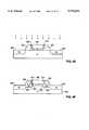
- FIGS. 4A-4Eshow cross-sectional views of successive process steps for forming a shallow junction in accordance with a fourth embodiment of the invention. It may be desirable to reduce the overlap between the gate electrode and the source/drain regions, as mentioned above. Lateral diffusion may occur as the dopant diffuses from the spacer, particularly if the dopant is boron. Similarly, after the dopant diffuses from the spacer into the substrate, a certain amount of lateral diffusion may occur during a subsequent thermal cycle. The amount of lateral diffusion depends on various parameters including the type of dopant, the temperature and duration of the thermal cycle, the device geometry, and so on.
- the lateral spacingcan be provided by insulative spacers that extend to the substrate.
- the primary difference between the fourth embodiment and the third embodimentis that in the fourth embodiment, the gate oxide outside the gate electrode is completely removed (as in the first embodiment), and the sidewall oxides are provided by oxide spacers that extend to the substrate and cover the edges of the gate oxide.
- the elements for the fourth embodimente.g., substrate 402, gate oxide 404, etc.
- the elements for the fourth embodimentare similar to elements of the third embodiment (e.g., substrate 302, gate oxide 304, etc.), and the description of related elements and process steps need not be repeated.
- gate oxide 404is formed on substrate 402, and polysilicon 406 is formed on gate oxide 404.
- Substrate 402is doped N-type.
- the gate electrode material and the gate insulator materialare patterned to provide the gate electrode and gate insulator.
- polysilicon 406is etched in a similar manner to polysilicon 106
- gate oxide 404is etched in a similar manner to gate oxide 104.
- insulative spacersare formed adjacent to the gate electrode. Unlike the previous embodiments, the insulative spacers extend to the substrate and cover the edges of the gate oxide as well. For instance, a second blanket layer of oxide (such as SiO 2 ) is deposited over substrate 402, and thereafter an anisotropic etch is applied to form oxide spacers 421 and 423. Oxide spacers 421 and 423 are formed on polysilicon edges 410 and 412, respectively, on gate oxide sidewalls 414 and 416, respectively, and on portions of substrate 402 adjacent to oxide sidewalls 414 and 416, respectively.
- oxide spacers 421 and 423are formed on polysilicon edges 410 and 412, respectively, on gate oxide sidewalls 414 and 416, respectively, and on portions of substrate 402 adjacent to oxide sidewalls 414 and 416, respectively.
- Oxide spacers 421 and 423each laterally extend about 700 angstroms along substrate 402 adjacent to gate oxide sidewalls 414 and 416, respectively. To ensure a high quality interface under the oxide spacers, it may be desirable to form a thin oxide layer (not shown) between the oxide spacers and the underlying substrate.
- the silicon-based spaceris formed over the substrate.
- the silicon-based spacerdoes not contact the gate insulator.
- polysilicon spacers 430 and 432contact the sides of oxide spacers 421 and 423, respectively, opposite polysilicon 406, and contact portions of substrate 402 outside oxide spacers 421 and 423, respectively.
- polysilicon spacers 430 and 432are laterally spaced from and electrically isolated from edges 410 and 412 of polysilicon 406 by oxide spacers 421 and 423, respectively.
- polysilicon spacers 430 and 432are doped without doping substrate 402.
- the dopant in the silicon-based spaceris diffused directly into the substrate to form a source or drain region.
- the boronis diffused directly into the underlying substrate without a retarding insulator layer therebetween.
- a significant amount of the rapidly diffusing boron atomslaterally diffuse beneath oxide spacers 421 and 423.
- shallow P+ regions 450 and 452 with a boron concentration in the range of 1 ⁇ 10 18 to 1 ⁇ 10 19 atoms/cm 3 and a depth in the range of 0.01 to 0.15 micronsform shallow junctions 454 and 456, respectively, which are substantially laterally aligned with edges 410 and 412, respectively, of polysilicon 406.
- Shallow regions 450 and 452provide drain and source regions, respectively, as opposed to lightly doped regions.
- spacers 430 and 432make electrical contact with regions 450 and 452, respectively, and therefore provide drain and source contacts, respectively.
- FIGS. 5A-5Eshow cross-sectional views of successive process steps for forming a shallow junction in accordance with a fifth embodiment of the invention.
- the sidewall insulatorcan be omitted by providing a gate electrode doped to a first conductivity type adjacent to a silicon-based spacer doped to a second conductivity type, such that the adjacent sidewalls form a PN junction.
- the PN junctioncan be reverse-biased, thereby electrically isolating the gate electrode from the spacer.
- the primary difference between the fifth embodiment and the third embodimentis that in the fifth embodiment, the sidewall oxides are omitted, and the spacers are formed adjacent to the polysilicon gate.
- the elements for the fifth embodimentare similar to elements of the third embodiment (e.g., substrate 302, gate oxide 304, etc.), and the description of related elements and process steps need not be repeated.
- gate oxide 504is formed on substrate 502, and polysilicon 506 is formed on gate oxide 504.
- polysilicon 506is etched in a similar manner to polysilicon 306, and gate oxide 504 is etched in a similar manner to gate oxide 304.
- the sidewall oxide(FIG. 3C) is omitted and spacers 530 and 532 are formed adjacent to edges 510 and 512, respectively, of polysilicon 506. Spacers 530 and 532 are doped P-type, and polysilicon 506 is doped N-type.
- FIG. 5Dshallow regions 550 and 552 are formed.
- FIGS. 6A-6Fshow cross-sectional views of successive process steps for forming a shallow junction in accordance with a sixth embodiment of the invention.
- Doping the silicon-based spacers before implanting the heavily doped regionsis not essential.
- the silicon-based spacerscan be doped during the implant step for the heavily doped regions of the drain and source, thereby reducing the number of implant steps.
- the primary difference between the sixth embodiment and the first embodimentis that in the sixth embodiment, the silicon-based spacers are formed undoped, and are subsequently doped when the heavily doped regions are implanted.
- the elements for the sixth embodimentare similar to elements of the first embodiment (e.g., substrate 102, gate oxide 104, etc.), and the description of related elements and process steps need not be repeated.
- gate oxide 604is formed on substrate 602, and polysilicon 606 is formed on gate oxide 604.
- polysilicon 606is etched in a similar manner to polysilicon 106, and gate oxide 604 is etched in a similar manner to gate oxide 104.
- thin sidewall oxides 620 and 622are formed on polysilicon edges 610 and 612, respectively.
- spacers 630 and 632are formed. However, unlike spacers 130 and 132, spacers 630 and 632 are formed undoped.
- FIG. 6Eheavily doped regions 640 and 642 are formed, and the implantation also serves to dope previously undoped spacers 630 and 632.
- An advantage to this approachis that spacers 630 and 632 need not be doped in a separate step.
- shallow regions 650 and 652are formed with shallow junctions 654 and 656 substantially laterally aligned with edges 610 and 612, respectively, of polysilicon 606.
- Further processing steps in the fabrication of IGFETstypically include forming a thick oxide layer over the active regions, forming contact windows in the oxide layer to expose the drain, source and gate electrode, forming appropriate interconnect metallization in the contact windows, and forming a passivation layer.
- subsequent high temperature process stepscan be used to supplement or replace the drive-in step to provide the desired anneal, activation, and drive-in functions.
- the lateral locations of the shallow junctionsbe precisely controlled.
- the gate electrode(except for the fifth embodiment) can be a conductor such as a metal, and the silicon-based spacers can be amorphous silicon, polysilicon, or other silicon-based materials capable of being doped N-type or P-type.
- the gate insulatorcan various dielectrics, and the sidewall insulator can also be various dielectrics such as silicon dioxide or silicon nitride.
- the sidewall insulatorcan be formed by various techniques including deposition, robe growth and rapid thermal anneal growth.
- the sidewall insulatorcan be a blanket layer that is etched in the regions where the silicon-based spacers are desired.
- the polysilicon gate electrodecan be doped after the silicon-based spacers are doped, for instance at the same time the heavily doped regions (outside the spacers) are implanted.
- the silicon-based spacerscan be deposited doped or undoped, and if deposited undoped can be doped either before or after the spacer etch.
- N-type or P-type dopantscan be used in any of the embodiments described above.
- the substratecan be recessed outside the gated electrode in any of the embodiments described above. The dopants can be diffused from the spacers to the substrate by applying various combinations of heat and pressure.
- the spacer insulatorcan be used for other dopants besides boron, although other dopants are more likely to accumulate in the spacer insulator without diffusing into the substrate.
- Other suitable P-type dopantsinclude boron B 10 , and boron B 11 , and BF X species such as BF 2 .
- the silicon-based spacerscan be removed and/or replaced by other spacers such as conventional oxide spacers.
- the inventionis particularly well-suited for fabricating N-channel MOSFETs, P-channel MOSFETs, and other types of IGFETs, particularly for high-performance microprocessors where high circuit density is essential. Although only a single FET has been shown for purposes of illustration, it is understood that in actual practice, many devices are fabricated on a single semiconductor wafer as widely practiced in the art. Accordingly, the invention is well-suited for use in an integrated circuit chip, as well as an electronic system including a microprocessor, a memory, and a system bus.
Landscapes
- Engineering & Computer Science (AREA)
- Physics & Mathematics (AREA)
- Condensed Matter Physics & Semiconductors (AREA)
- General Physics & Mathematics (AREA)
- Manufacturing & Machinery (AREA)
- Computer Hardware Design (AREA)
- Microelectronics & Electronic Packaging (AREA)
- Power Engineering (AREA)
- Insulated Gate Type Field-Effect Transistor (AREA)
Abstract
Description
Claims (57)
Priority Applications (1)
| Application Number | Priority Date | Filing Date | Title |
|---|---|---|---|
| US08/703,273US5710054A (en) | 1996-08-26 | 1996-08-26 | Method of forming a shallow junction by diffusion from a silicon-based spacer |
Applications Claiming Priority (1)
| Application Number | Priority Date | Filing Date | Title |
|---|---|---|---|
| US08/703,273US5710054A (en) | 1996-08-26 | 1996-08-26 | Method of forming a shallow junction by diffusion from a silicon-based spacer |
Publications (1)
| Publication Number | Publication Date |
|---|---|
| US5710054Atrue US5710054A (en) | 1998-01-20 |
Family
ID=24824731
Family Applications (1)
| Application Number | Title | Priority Date | Filing Date |
|---|---|---|---|
| US08/703,273Expired - LifetimeUS5710054A (en) | 1996-08-26 | 1996-08-26 | Method of forming a shallow junction by diffusion from a silicon-based spacer |
Country Status (1)
| Country | Link |
|---|---|
| US (1) | US5710054A (en) |
Cited By (53)
| Publication number | Priority date | Publication date | Assignee | Title |
|---|---|---|---|---|
| US5930617A (en)* | 1998-03-25 | 1999-07-27 | Texas Instruments-Acer Incorporated | Method of forming deep sub-micron CMOS transistors with self-aligned silicided contact and extended S/D junction |
| US5937301A (en)* | 1997-08-19 | 1999-08-10 | Advanced Micro Devices | Method of making a semiconductor device having sidewall spacers with improved profiles |
| US5981321A (en)* | 1996-12-28 | 1999-11-09 | National Science Council | Forming CMOS transistor using diffusion source and wet/dry oxidation |
| US5989966A (en)* | 1997-12-15 | 1999-11-23 | Taiwan Semiconductor Manufacturing Company, Ltd. | Method and a deep sub-micron field effect transistor structure for suppressing short channel effects |
| US5998294A (en)* | 1998-04-29 | 1999-12-07 | The United States Of America As Represented By The Secretary Of The Navy | Method for forming improved electrical contacts on non-planar structures |
| US6093610A (en)* | 1998-06-16 | 2000-07-25 | Texas Instruments Incorporated | Self-aligned pocket process for deep sub-0.1 μm CMOS devices and the device |
| US6117719A (en)* | 1997-12-18 | 2000-09-12 | Advanced Micro Devices, Inc. | Oxide spacers as solid sources for gallium dopant introduction |
| US6136636A (en)* | 1998-03-25 | 2000-10-24 | Texas Instruments - Acer Incorporated | Method of manufacturing deep sub-micron CMOS transistors |
| US6159814A (en)* | 1997-11-12 | 2000-12-12 | Advanced, Micro Devices, Inc. | Spacer formation by poly stack dopant profile design |
| US6255183B1 (en)* | 1997-05-23 | 2001-07-03 | U.S. Phillips Corporation | Manufacture of a semiconductor device with a MOS transistor having an LDD structure using SiGe spacers |
| US6274446B1 (en)* | 1999-09-28 | 2001-08-14 | International Business Machines Corporation | Method for fabricating abrupt source/drain extensions with controllable gate electrode overlap |
| US6323077B1 (en)* | 1999-12-30 | 2001-11-27 | Vanguard International Semiconductor Corporation | Inverse source/drain process using disposable sidewall spacer |
| US6333251B1 (en)* | 1999-08-17 | 2001-12-25 | Samsung Electronics Co., Ltd. | Method of fabricating gate structure of semiconductor device for repairing damage to gate oxide layer |
| US6372588B2 (en) | 1997-04-21 | 2002-04-16 | Advanced Micro Devices, Inc. | Method of making an IGFET using solid phase diffusion to dope the gate, source and drain |
| US6506653B1 (en) | 2000-03-13 | 2003-01-14 | International Business Machines Corporation | Method using disposable and permanent films for diffusion and implant doping |
| US6566208B2 (en)* | 2001-07-25 | 2003-05-20 | Chartered Semiconductor Manufacturing Ltd. | Method to form elevated source/drain using poly spacer |
| US6627502B1 (en) | 2002-10-24 | 2003-09-30 | Taiwan Semiconductor Manufacturing Company | Method for forming high concentration shallow junctions for short channel MOSFETs |
| US6642134B2 (en)* | 1999-09-22 | 2003-11-04 | Advanced Micro Devices, Inc. | Semiconductor processing employing a semiconductor spacer |
| US20040126976A1 (en)* | 2002-12-30 | 2004-07-01 | Dongbu Electronics Co., Ltd. | Method of manufacturing a semiconductor device |
| US20040222465A1 (en)* | 2001-07-17 | 2004-11-11 | Renesas Technology Corp. | Semiconductor device and method of manufacturing same |
| US20050112832A1 (en)* | 2002-05-17 | 2005-05-26 | Renesas Technology Corp. | Method of manufacturing semiconductor device |
| US20050151203A1 (en)* | 2004-01-09 | 2005-07-14 | Taiwan Semiconductor Manufacturing Co. | Temporary self-aligned stop layer is applied on silicon sidewall |
| US20050167738A1 (en)* | 2001-07-02 | 2005-08-04 | Hiroyuki Tanaka | Semiconductor device and manufacturing method of the same |
| US20050167756A1 (en)* | 2004-01-29 | 2005-08-04 | Enpirion, Incorporated | Laterally diffused metal oxide semiconductor device and method of forming the same |
| US20060040441A1 (en)* | 2004-08-23 | 2006-02-23 | Lotfi Ashraf W | Method of forming an integrated circuit employable with a power converter |
| US20060038238A1 (en)* | 2004-08-23 | 2006-02-23 | Lotfi Ashraf W | Integrated circuit incorporating higher voltage devices and low voltage devices therein |
| US20060040451A1 (en)* | 2004-08-23 | 2006-02-23 | Lotfi Ashraf W | Method of forming an integrated circuit employable with a power converter |
| US20060040449A1 (en)* | 2004-08-23 | 2006-02-23 | Lotfi Ashraf W | Method of forming an integrated circuit incorporating higher voltage devices and low voltage devices therein |
| US20060038237A1 (en)* | 2004-08-23 | 2006-02-23 | Lotfi Ashraf W | Integrated circuit incorporating higher voltage devices and low voltage devices therein |
| US20060039224A1 (en)* | 2004-08-23 | 2006-02-23 | Lotfi Ashraf W | Integrated circuit employable with a power converter |
| US20060040452A1 (en)* | 2004-08-23 | 2006-02-23 | Lotfi Ashraf W | Method of forming an integrated circuit incorporating higher voltage devices and low voltage devices therein |
| US20060038225A1 (en)* | 2004-08-23 | 2006-02-23 | Lotfi Ashraf W | Integrated circuit employable with a power converter |
| US20060186558A1 (en)* | 2003-05-29 | 2006-08-24 | Seung-Jae Baik | Methods of fabricating scalable two transistor memory devices |
| US20070052008A1 (en)* | 2005-09-05 | 2007-03-08 | Chih-Ping Chung | Memory structure with high coupling ratio |
| US20070224764A1 (en)* | 2006-03-27 | 2007-09-27 | Yamaha Corporation | Method for manufacturing insulated-gate type field effect transistor |
| US20080093633A1 (en)* | 2006-10-18 | 2008-04-24 | United Microelectronics Corp. | Complementary metal-oxide-semiconductor (cmos) image sensor and fabricating method thereof |
| US20080142884A1 (en)* | 2006-12-19 | 2008-06-19 | Yong-Soo Cho | Semiconductor device |
| US20080258180A1 (en)* | 2006-01-09 | 2008-10-23 | International Business Machines Corporation | Cross-section hourglass shaped channel region for charge carrier mobility modification |
| US20100044789A1 (en)* | 2004-01-29 | 2010-02-25 | Enpirion, Incorporated | Integrated Circuit with a Laterally Diffused Metal Oxide Semiconductor Device and Method of Forming the Same |
| US20100052050A1 (en)* | 2004-01-29 | 2010-03-04 | Enpirion, Incorporated | Integrated Circuit with a Laterally Diffused Metal Oxide Semiconductor Device and Method of Forming the Same |
| US20100052049A1 (en)* | 2004-01-29 | 2010-03-04 | Enpirion, Incorporated, A Delaware Corporation | Integrated Circuit with a Laterally Diffused Metal Oxide Semiconductor Device and Method of Forming the Same |
| US20100052051A1 (en)* | 2004-01-29 | 2010-03-04 | Enpirion, Incorporated, A Delaware Corporation | Integrated Circuit with a Laterally Diffused Metal Oxide Semiconductor Device and Method of Forming the Same |
| US20110049621A1 (en)* | 2004-01-29 | 2011-03-03 | Enpirion Incorporated, A Delaware Corporation | Integrated Circuit with a Laterally Diffused Metal Oxide Semiconductor Device and Method of Forming the Same |
| US8253196B2 (en) | 2004-01-29 | 2012-08-28 | Enpirion, Inc. | Integrated circuit with a laterally diffused metal oxide semiconductor device and method of forming the same |
| US9536938B1 (en) | 2013-11-27 | 2017-01-03 | Altera Corporation | Semiconductor device including a resistor metallic layer and method of forming the same |
| US9608066B1 (en)* | 2015-09-29 | 2017-03-28 | International Business Machines Corporation | High-K spacer for extension-free CMOS devices with high mobility channel materials |
| EP3053198A4 (en)* | 2013-10-01 | 2017-05-03 | Vishay General Semiconductor LLC | Zener diode having a polysilicon layer for improved reverse surge capability and decreased leakage current |
| US9673192B1 (en) | 2013-11-27 | 2017-06-06 | Altera Corporation | Semiconductor device including a resistor metallic layer and method of forming the same |
| FR3046875A1 (en)* | 2016-01-19 | 2017-07-21 | Commissariat Energie Atomique | PROCESS FOR PRODUCING A TRANSISTOR |
| US10020739B2 (en) | 2014-03-27 | 2018-07-10 | Altera Corporation | Integrated current replicator and method of operating the same |
| US10103627B2 (en) | 2015-02-26 | 2018-10-16 | Altera Corporation | Packaged integrated circuit including a switch-mode regulator and method of forming the same |
| CN112582476A (en)* | 2020-12-09 | 2021-03-30 | 全芯智造技术有限公司 | Semiconductor device and method of forming the same |
| US11145739B2 (en)* | 2016-03-04 | 2021-10-12 | Intel Corporation | Field effect transistors with a gated oxide semiconductor source/drain spacer |
Citations (7)
| Publication number | Priority date | Publication date | Assignee | Title |
|---|---|---|---|---|
| US5064776A (en)* | 1990-10-03 | 1991-11-12 | Micron Technology, Inc. | Method of forming buried contact between polysilicon gate and diffusion area |
| US5391508A (en)* | 1992-12-21 | 1995-02-21 | Sharp Kabushiki Kaisha | Method of forming semiconductor transistor devices |
| US5457060A (en)* | 1994-06-20 | 1995-10-10 | Winbond Electronics Corporation | Process for manufactuirng MOSFET having relatively shallow junction of doped region |
| US5466958A (en)* | 1992-10-30 | 1995-11-14 | Kabushiki Kaisha Toshiba | MOS-type semiconductor device having electrode structure capable of coping with short-channel effect and manufacturing method thereof |
| US5504031A (en)* | 1995-07-03 | 1996-04-02 | Taiwan Semiconductor Manufacturing Company Ltd. | Elevated source/drain with solid phase diffused source/drain extension for deep sub-micron mosfets |
| US5559049A (en)* | 1994-07-25 | 1996-09-24 | Hyundai Electronics Insustries Co., Ltd | Method of manufacturing a semiconductor device |
| US5591650A (en)* | 1995-06-08 | 1997-01-07 | Taiwan Semiconductor Manufacturing Company Ltd. | Method of making a body contacted SOI MOSFET |
- 1996
- 1996-08-26USUS08/703,273patent/US5710054A/ennot_activeExpired - Lifetime
Patent Citations (7)
| Publication number | Priority date | Publication date | Assignee | Title |
|---|---|---|---|---|
| US5064776A (en)* | 1990-10-03 | 1991-11-12 | Micron Technology, Inc. | Method of forming buried contact between polysilicon gate and diffusion area |
| US5466958A (en)* | 1992-10-30 | 1995-11-14 | Kabushiki Kaisha Toshiba | MOS-type semiconductor device having electrode structure capable of coping with short-channel effect and manufacturing method thereof |
| US5391508A (en)* | 1992-12-21 | 1995-02-21 | Sharp Kabushiki Kaisha | Method of forming semiconductor transistor devices |
| US5457060A (en)* | 1994-06-20 | 1995-10-10 | Winbond Electronics Corporation | Process for manufactuirng MOSFET having relatively shallow junction of doped region |
| US5559049A (en)* | 1994-07-25 | 1996-09-24 | Hyundai Electronics Insustries Co., Ltd | Method of manufacturing a semiconductor device |
| US5591650A (en)* | 1995-06-08 | 1997-01-07 | Taiwan Semiconductor Manufacturing Company Ltd. | Method of making a body contacted SOI MOSFET |
| US5504031A (en)* | 1995-07-03 | 1996-04-02 | Taiwan Semiconductor Manufacturing Company Ltd. | Elevated source/drain with solid phase diffused source/drain extension for deep sub-micron mosfets |
Cited By (92)
| Publication number | Priority date | Publication date | Assignee | Title |
|---|---|---|---|---|
| US5981321A (en)* | 1996-12-28 | 1999-11-09 | National Science Council | Forming CMOS transistor using diffusion source and wet/dry oxidation |
| US6372588B2 (en) | 1997-04-21 | 2002-04-16 | Advanced Micro Devices, Inc. | Method of making an IGFET using solid phase diffusion to dope the gate, source and drain |
| US6255183B1 (en)* | 1997-05-23 | 2001-07-03 | U.S. Phillips Corporation | Manufacture of a semiconductor device with a MOS transistor having an LDD structure using SiGe spacers |
| US5937301A (en)* | 1997-08-19 | 1999-08-10 | Advanced Micro Devices | Method of making a semiconductor device having sidewall spacers with improved profiles |
| US6159814A (en)* | 1997-11-12 | 2000-12-12 | Advanced, Micro Devices, Inc. | Spacer formation by poly stack dopant profile design |
| US5989966A (en)* | 1997-12-15 | 1999-11-23 | Taiwan Semiconductor Manufacturing Company, Ltd. | Method and a deep sub-micron field effect transistor structure for suppressing short channel effects |
| US6157064A (en)* | 1997-12-15 | 2000-12-05 | Taiwan Semiconductor Manufacturing Company Ltd. | Method and a deep sub-micron field effect transistor structure for suppressing short channel effects |
| US6117719A (en)* | 1997-12-18 | 2000-09-12 | Advanced Micro Devices, Inc. | Oxide spacers as solid sources for gallium dopant introduction |
| US5930617A (en)* | 1998-03-25 | 1999-07-27 | Texas Instruments-Acer Incorporated | Method of forming deep sub-micron CMOS transistors with self-aligned silicided contact and extended S/D junction |
| US6136636A (en)* | 1998-03-25 | 2000-10-24 | Texas Instruments - Acer Incorporated | Method of manufacturing deep sub-micron CMOS transistors |
| US5998294A (en)* | 1998-04-29 | 1999-12-07 | The United States Of America As Represented By The Secretary Of The Navy | Method for forming improved electrical contacts on non-planar structures |
| US6093610A (en)* | 1998-06-16 | 2000-07-25 | Texas Instruments Incorporated | Self-aligned pocket process for deep sub-0.1 μm CMOS devices and the device |
| US6333251B1 (en)* | 1999-08-17 | 2001-12-25 | Samsung Electronics Co., Ltd. | Method of fabricating gate structure of semiconductor device for repairing damage to gate oxide layer |
| US6642134B2 (en)* | 1999-09-22 | 2003-11-04 | Advanced Micro Devices, Inc. | Semiconductor processing employing a semiconductor spacer |
| US6274446B1 (en)* | 1999-09-28 | 2001-08-14 | International Business Machines Corporation | Method for fabricating abrupt source/drain extensions with controllable gate electrode overlap |
| US6407436B1 (en) | 1999-09-28 | 2002-06-18 | International Business Machines Corporation | Semiconductor device with abrupt source/drain extensions with controllable gate electrode overlap |
| US6323077B1 (en)* | 1999-12-30 | 2001-11-27 | Vanguard International Semiconductor Corporation | Inverse source/drain process using disposable sidewall spacer |
| US6506653B1 (en) | 2000-03-13 | 2003-01-14 | International Business Machines Corporation | Method using disposable and permanent films for diffusion and implant doping |
| US6924200B2 (en) | 2000-03-13 | 2005-08-02 | International Business Machines Corporation | Methods using disposable and permanent films for diffusion and implantation doping |
| US7364995B2 (en)* | 2001-07-02 | 2008-04-29 | Oki Electric Industry Co., Ltd. | Method of forming reduced short channel field effect transistor |
| US20050167738A1 (en)* | 2001-07-02 | 2005-08-04 | Hiroyuki Tanaka | Semiconductor device and manufacturing method of the same |
| US7109553B2 (en) | 2001-07-17 | 2006-09-19 | Renesas Technology Corp. | Semiconductor device and method of manufacturing same |
| US20040222465A1 (en)* | 2001-07-17 | 2004-11-11 | Renesas Technology Corp. | Semiconductor device and method of manufacturing same |
| US20060273394A1 (en)* | 2001-07-17 | 2006-12-07 | Renesas Technology Corp. | Semiconductor device and method of manufacturing same |
| EP1280191A3 (en)* | 2001-07-25 | 2003-08-06 | Chartered Semiconductor Manufacturing Pte Ltd. | A method to form elevated source/drain regions using polysilicon spacers |
| US6566208B2 (en)* | 2001-07-25 | 2003-05-20 | Chartered Semiconductor Manufacturing Ltd. | Method to form elevated source/drain using poly spacer |
| US20050112832A1 (en)* | 2002-05-17 | 2005-05-26 | Renesas Technology Corp. | Method of manufacturing semiconductor device |
| US6627502B1 (en) | 2002-10-24 | 2003-09-30 | Taiwan Semiconductor Manufacturing Company | Method for forming high concentration shallow junctions for short channel MOSFETs |
| US7022576B2 (en)* | 2002-12-30 | 2006-04-04 | Dongbuanam Semiconductor Inc. | Method of manufacturing a semiconductor device |
| US20040126976A1 (en)* | 2002-12-30 | 2004-07-01 | Dongbu Electronics Co., Ltd. | Method of manufacturing a semiconductor device |
| US7566615B2 (en)* | 2003-05-29 | 2009-07-28 | Samsung Electronics Co., Ltd. | Methods of fabricating scalable two transistor memory devices |
| US20060186558A1 (en)* | 2003-05-29 | 2006-08-24 | Seung-Jae Baik | Methods of fabricating scalable two transistor memory devices |
| US6972222B2 (en)* | 2004-01-09 | 2005-12-06 | Taiwan Semiconductor Manufacturing Company | Temporary self-aligned stop layer is applied on silicon sidewall |
| US20050151203A1 (en)* | 2004-01-09 | 2005-07-14 | Taiwan Semiconductor Manufacturing Co. | Temporary self-aligned stop layer is applied on silicon sidewall |
| US8212315B2 (en) | 2004-01-29 | 2012-07-03 | Enpirion, Inc. | Integrated circuit with a laterally diffused metal oxide semiconductor device and method of forming the same |
| US8716790B2 (en) | 2004-01-29 | 2014-05-06 | Enpirion, Inc. | Laterally diffused metal oxide semiconductor device and method of forming the same |
| US9680008B2 (en) | 2004-01-29 | 2017-06-13 | Empirion, Inc. | Laterally diffused metal oxide semiconductor device and method of forming the same |
| US8987815B2 (en) | 2004-01-29 | 2015-03-24 | Enpirion, Inc. | Integrated circuit with a laterally diffused metal oxide semiconductor device and method of forming the same |
| US8633540B2 (en) | 2004-01-29 | 2014-01-21 | Enpirion, Inc. | Integrated circuit with a laterally diffused metal oxide semiconductor device and method of forming the same |
| US20060081937A1 (en)* | 2004-01-29 | 2006-04-20 | Lotfi Ashraf W | Laterally diffused metal oxide semiconductor device and method of forming the same |
| US8253195B2 (en) | 2004-01-29 | 2012-08-28 | Enpirion, Inc. | Integrated circuit with a laterally diffused metal oxide semiconductor device and method of forming the same |
| US8253197B2 (en) | 2004-01-29 | 2012-08-28 | Enpirion, Inc. | Integrated circuit with a laterally diffused metal oxide semiconductor device and method of forming the same |
| US8253196B2 (en) | 2004-01-29 | 2012-08-28 | Enpirion, Inc. | Integrated circuit with a laterally diffused metal oxide semiconductor device and method of forming the same |
| US8212316B2 (en) | 2004-01-29 | 2012-07-03 | Enpirion, Inc. | Integrated circuit with a laterally diffused metal oxide semiconductor device and method of forming the same |
| US8212317B2 (en) | 2004-01-29 | 2012-07-03 | Enpirion, Inc. | Integrated circuit with a laterally diffused metal oxide semiconductor device and method of forming the same |
| US20050167756A1 (en)* | 2004-01-29 | 2005-08-04 | Enpirion, Incorporated | Laterally diffused metal oxide semiconductor device and method of forming the same |
| US20110049621A1 (en)* | 2004-01-29 | 2011-03-03 | Enpirion Incorporated, A Delaware Corporation | Integrated Circuit with a Laterally Diffused Metal Oxide Semiconductor Device and Method of Forming the Same |
| US7759184B2 (en) | 2004-01-29 | 2010-07-20 | Enpirion, Inc. | Laterally diffused metal oxide semiconductor device and method of forming the same |
| US20100052051A1 (en)* | 2004-01-29 | 2010-03-04 | Enpirion, Incorporated, A Delaware Corporation | Integrated Circuit with a Laterally Diffused Metal Oxide Semiconductor Device and Method of Forming the Same |
| US7230302B2 (en)* | 2004-01-29 | 2007-06-12 | Enpirion, Inc. | Laterally diffused metal oxide semiconductor device and method of forming the same |
| US20100052049A1 (en)* | 2004-01-29 | 2010-03-04 | Enpirion, Incorporated, A Delaware Corporation | Integrated Circuit with a Laterally Diffused Metal Oxide Semiconductor Device and Method of Forming the Same |
| US7244994B2 (en)* | 2004-01-29 | 2007-07-17 | Enpirion, Inc. | Laterally diffused metal oxide semiconductor device and method of forming the same |
| US20070224752A1 (en)* | 2004-01-29 | 2007-09-27 | Lotfi Ashraf W | Laterally diffused metal oxide semiconductor device and method of forming the same |
| US20100052050A1 (en)* | 2004-01-29 | 2010-03-04 | Enpirion, Incorporated | Integrated Circuit with a Laterally Diffused Metal Oxide Semiconductor Device and Method of Forming the Same |
| US20070284658A1 (en)* | 2004-01-29 | 2007-12-13 | Lotfi Ashraf W | Laterally Diffused Metal Oxide Semiconductor Device and Method of Forming the Same |
| US20100044789A1 (en)* | 2004-01-29 | 2010-02-25 | Enpirion, Incorporated | Integrated Circuit with a Laterally Diffused Metal Oxide Semiconductor Device and Method of Forming the Same |
| US20060040449A1 (en)* | 2004-08-23 | 2006-02-23 | Lotfi Ashraf W | Method of forming an integrated circuit incorporating higher voltage devices and low voltage devices therein |
| US20060038238A1 (en)* | 2004-08-23 | 2006-02-23 | Lotfi Ashraf W | Integrated circuit incorporating higher voltage devices and low voltage devices therein |
| US20060038225A1 (en)* | 2004-08-23 | 2006-02-23 | Lotfi Ashraf W | Integrated circuit employable with a power converter |
| US7015544B2 (en) | 2004-08-23 | 2006-03-21 | Enpirion, Inc. | Intergrated circuit employable with a power converter |
| US20060040452A1 (en)* | 2004-08-23 | 2006-02-23 | Lotfi Ashraf W | Method of forming an integrated circuit incorporating higher voltage devices and low voltage devices therein |
| US20060040441A1 (en)* | 2004-08-23 | 2006-02-23 | Lotfi Ashraf W | Method of forming an integrated circuit employable with a power converter |
| US20060039224A1 (en)* | 2004-08-23 | 2006-02-23 | Lotfi Ashraf W | Integrated circuit employable with a power converter |
| US7335948B2 (en) | 2004-08-23 | 2008-02-26 | Enpirion, Inc. | Integrated circuit incorporating higher voltage devices and low voltage devices therein |
| US20060038237A1 (en)* | 2004-08-23 | 2006-02-23 | Lotfi Ashraf W | Integrated circuit incorporating higher voltage devices and low voltage devices therein |
| US7232733B2 (en) | 2004-08-23 | 2007-06-19 | Enpirion, Inc. | Method of forming an integrated circuit incorporating higher voltage devices and low voltage devices therein |
| US7229886B2 (en) | 2004-08-23 | 2007-06-12 | Enpirion, Inc. | Method of forming an integrated circuit incorporating higher voltage devices and low voltage devices therein |
| US7214985B2 (en) | 2004-08-23 | 2007-05-08 | Enpirion, Inc. | Integrated circuit incorporating higher voltage devices and low voltage devices therein |
| US7186606B2 (en) | 2004-08-23 | 2007-03-06 | Enpirion, Inc. | Method of forming an integrated circuit employable with a power converter |
| US7195981B2 (en) | 2004-08-23 | 2007-03-27 | Enpirion, Inc. | Method of forming an integrated circuit employable with a power converter |
| US7190026B2 (en) | 2004-08-23 | 2007-03-13 | Enpirion, Inc. | Integrated circuit employable with a power converter |
| US20060040451A1 (en)* | 2004-08-23 | 2006-02-23 | Lotfi Ashraf W | Method of forming an integrated circuit employable with a power converter |
| US20070052008A1 (en)* | 2005-09-05 | 2007-03-08 | Chih-Ping Chung | Memory structure with high coupling ratio |
| US7535050B2 (en)* | 2005-09-05 | 2009-05-19 | Promos Technologies Inc. | Memory structure with high coupling ratio |
| US7863197B2 (en)* | 2006-01-09 | 2011-01-04 | International Business Machines Corporation | Method of forming a cross-section hourglass shaped channel region for charge carrier mobility modification |
| US20080258180A1 (en)* | 2006-01-09 | 2008-10-23 | International Business Machines Corporation | Cross-section hourglass shaped channel region for charge carrier mobility modification |
| US20070224764A1 (en)* | 2006-03-27 | 2007-09-27 | Yamaha Corporation | Method for manufacturing insulated-gate type field effect transistor |
| US7659173B2 (en)* | 2006-03-27 | 2010-02-09 | Yamaha Corporation | Method for manufacturing insulated-gate type field effect transistor |
| US20080093633A1 (en)* | 2006-10-18 | 2008-04-24 | United Microelectronics Corp. | Complementary metal-oxide-semiconductor (cmos) image sensor and fabricating method thereof |
| US20080142884A1 (en)* | 2006-12-19 | 2008-06-19 | Yong-Soo Cho | Semiconductor device |
| EP3053198A4 (en)* | 2013-10-01 | 2017-05-03 | Vishay General Semiconductor LLC | Zener diode having a polysilicon layer for improved reverse surge capability and decreased leakage current |
| US9673192B1 (en) | 2013-11-27 | 2017-06-06 | Altera Corporation | Semiconductor device including a resistor metallic layer and method of forming the same |
| US9536938B1 (en) | 2013-11-27 | 2017-01-03 | Altera Corporation | Semiconductor device including a resistor metallic layer and method of forming the same |
| US10020739B2 (en) | 2014-03-27 | 2018-07-10 | Altera Corporation | Integrated current replicator and method of operating the same |
| US10103627B2 (en) | 2015-02-26 | 2018-10-16 | Altera Corporation | Packaged integrated circuit including a switch-mode regulator and method of forming the same |
| US9608066B1 (en)* | 2015-09-29 | 2017-03-28 | International Business Machines Corporation | High-K spacer for extension-free CMOS devices with high mobility channel materials |
| FR3046875A1 (en)* | 2016-01-19 | 2017-07-21 | Commissariat Energie Atomique | PROCESS FOR PRODUCING A TRANSISTOR |
| US10014386B2 (en) | 2016-01-19 | 2018-07-03 | Commissariat A L'energie Atomique Et Aux Energies Alternatives | Method of manufacturing a transistor |
| US11145739B2 (en)* | 2016-03-04 | 2021-10-12 | Intel Corporation | Field effect transistors with a gated oxide semiconductor source/drain spacer |
| US12376362B2 (en) | 2016-03-04 | 2025-07-29 | Intel Corporation | Field effect transistors with a gated oxide semiconductor source/drain spacer |
| CN112582476A (en)* | 2020-12-09 | 2021-03-30 | 全芯智造技术有限公司 | Semiconductor device and method of forming the same |
| CN112582476B (en)* | 2020-12-09 | 2022-05-06 | 全芯智造技术有限公司 | Semiconductor device and method of forming the same |
Similar Documents
| Publication | Publication Date | Title |
|---|---|---|
| US5710054A (en) | Method of forming a shallow junction by diffusion from a silicon-based spacer | |
| US5930642A (en) | Transistor with buried insulative layer beneath the channel region | |
| US5972783A (en) | Method for fabricating a semiconductor device having a nitrogen diffusion layer | |
| US5648286A (en) | Method of making asymmetrical transistor with lightly doped drain region, heavily doped source and drain regions, and ultra-heavily doped source region | |
| US6201278B1 (en) | Trench transistor with insulative spacers | |
| US6509241B2 (en) | Process for fabricating an MOS device having highly-localized halo regions | |
| US6833307B1 (en) | Method for manufacturing a semiconductor component having an early halo implant | |
| US5656518A (en) | Method for fabrication of a non-symmetrical transistor | |
| US5663079A (en) | Method of making increased density MOS-gated semiconductor devices | |
| US6888176B1 (en) | Thyrister semiconductor device | |
| KR100223846B1 (en) | Semiconductor device and manufacturing method thereof | |
| US6197645B1 (en) | Method of making an IGFET with elevated source/drain regions in close proximity to gate with sloped sidewalls | |
| US7804107B1 (en) | Thyristor semiconductor device and method of manufacture | |
| JP2002520851A (en) | Method for manufacturing power semiconductor device | |
| US5654215A (en) | Method for fabrication of a non-symmetrical transistor | |
| US5869378A (en) | Method of reducing overlap between gate electrode and LDD region | |
| US7129564B2 (en) | Structure and method of forming a notched gate field effect transistor | |
| US6031272A (en) | MOS type semiconductor device having an impurity diffusion layer with a nonuniform impurity concentration profile in a channel region | |
| US6027978A (en) | Method of making an IGFET with a non-uniform lateral doping profile in the channel region | |
| US7208383B1 (en) | Method of manufacturing a semiconductor component | |
| US6261885B1 (en) | Method for forming integrated circuit gate conductors from dual layers of polysilicon | |
| US5212106A (en) | Optimizing doping control in short channel MOS | |
| US6576521B1 (en) | Method of forming semiconductor device with LDD structure | |
| US5877058A (en) | Method of forming an insulated-gate field-effect transistor with metal spacers | |
| US6188114B1 (en) | Method of forming an insulated-gate field-effect transistor with metal spacers |
Legal Events
| Date | Code | Title | Description |
|---|---|---|---|
| AS | Assignment | Owner name:ADVANCED MICRO DEVICES, INC., CALIFORNIA Free format text:ASSIGNMENT OF ASSIGNORS INTEREST;ASSIGNORS:GARDNER, MARK I.;DAWSON, ROBERT;FULFORD, H. JIM, JR.;AND OTHERS;REEL/FRAME:008179/0270 Effective date:19960816 | |
| FEPP | Fee payment procedure | Free format text:PAYOR NUMBER ASSIGNED (ORIGINAL EVENT CODE: ASPN); ENTITY STATUS OF PATENT OWNER: LARGE ENTITY | |
| STCF | Information on status: patent grant | Free format text:PATENTED CASE | |
| CC | Certificate of correction | ||
| FPAY | Fee payment | Year of fee payment:4 | |
| FPAY | Fee payment | Year of fee payment:8 | |
| FPAY | Fee payment | Year of fee payment:12 | |
| AS | Assignment | Owner name:GLOBALFOUNDRIES INC., CAYMAN ISLANDS Free format text:AFFIRMATION OF PATENT ASSIGNMENT;ASSIGNOR:ADVANCED MICRO DEVICES, INC.;REEL/FRAME:023119/0083 Effective date:20090630 | |
| AS | Assignment | Owner name:GLOBALFOUNDRIES U.S. INC., NEW YORK Free format text:RELEASE BY SECURED PARTY;ASSIGNOR:WILMINGTON TRUST, NATIONAL ASSOCIATION;REEL/FRAME:056987/0001 Effective date:20201117 |