US5708567A - Ball grid array semiconductor package with ring-type heat sink - Google Patents
Ball grid array semiconductor package with ring-type heat sinkDownload PDFInfo
- Publication number
- US5708567A US5708567AUS08/748,937US74893796AUS5708567AUS 5708567 AUS5708567 AUS 5708567AUS 74893796 AUS74893796 AUS 74893796AUS 5708567 AUS5708567 AUS 5708567A
- Authority
- US
- United States
- Prior art keywords
- heat sink
- package
- pcb
- semiconductor package
- chip
- Prior art date
- Legal status (The legal status is an assumption and is not a legal conclusion. Google has not performed a legal analysis and makes no representation as to the accuracy of the status listed.)
- Expired - Lifetime
Links
- 239000004065semiconductorSubstances0.000titleclaimsabstractdescription42
- 239000008393encapsulating agentSubstances0.000claimsabstractdescription20
- RYGMFSIKBFXOCR-UHFFFAOYSA-NCopperChemical compound[Cu]RYGMFSIKBFXOCR-UHFFFAOYSA-N0.000claimsabstractdescription9
- 229910000881Cu alloyInorganic materials0.000claimsabstractdescription9
- 229910052802copperInorganic materials0.000claimsabstractdescription9
- 239000010949copperSubstances0.000claimsabstractdescription9
- 229910000679solderInorganic materials0.000claimsdescription15
- PXHVJJICTQNCMI-UHFFFAOYSA-NNickelChemical compound[Ni]PXHVJJICTQNCMI-UHFFFAOYSA-N0.000claimsdescription11
- 239000004593EpoxySubstances0.000claimsdescription4
- 229910052759nickelInorganic materials0.000claimsdescription4
- 229910001020Au alloyInorganic materials0.000claimsdescription2
- VYZAMTAEIAYCRO-UHFFFAOYSA-NChromiumChemical compound[Cr]VYZAMTAEIAYCRO-UHFFFAOYSA-N0.000claimsdescription2
- 229910000990Ni alloyInorganic materials0.000claimsdescription2
- 229910052782aluminiumInorganic materials0.000claimsdescription2
- XAGFODPZIPBFFR-UHFFFAOYSA-NaluminiumChemical compound[Al]XAGFODPZIPBFFR-UHFFFAOYSA-N0.000claimsdescription2
- 229910052751metalInorganic materials0.000claimsdescription2
- 239000002184metalSubstances0.000claimsdescription2
- 238000005476solderingMethods0.000claimsdescription2
- 239000010935stainless steelSubstances0.000claimsdescription2
- 229910001220stainless steelInorganic materials0.000claimsdescription2
- 238000003466weldingMethods0.000claimsdescription2
- 239000003353gold alloySubstances0.000claims1
- 230000000694effectsEffects0.000abstractdescription6
- SXHLTVKPNQVZGL-UHFFFAOYSA-N1,2-dichloro-3-(3-chlorophenyl)benzeneChemical compoundClC1=CC=CC(C=2C(=C(Cl)C=CC=2)Cl)=C1SXHLTVKPNQVZGL-UHFFFAOYSA-N0.000description24
- 238000010276constructionMethods0.000description10
- 229920005989resinPolymers0.000description5
- 239000011347resinSubstances0.000description5
- 230000017525heat dissipationEffects0.000description4
- 150000001875compoundsChemical class0.000description3
- BQCADISMDOOEFD-UHFFFAOYSA-NSilverChemical compound[Ag]BQCADISMDOOEFD-UHFFFAOYSA-N0.000description2
- 230000008054signal transmissionEffects0.000description2
- 229910052709silverInorganic materials0.000description2
- 239000004332silverSubstances0.000description2
- JYEUMXHLPRZUAT-UHFFFAOYSA-N1,2,3-triazineChemical compoundC1=CN=NN=C1JYEUMXHLPRZUAT-UHFFFAOYSA-N0.000description1
- XQUPVDVFXZDTLT-UHFFFAOYSA-N1-[4-[[4-(2,5-dioxopyrrol-1-yl)phenyl]methyl]phenyl]pyrrole-2,5-dioneChemical compoundO=C1C=CC(=O)N1C(C=C1)=CC=C1CC1=CC=C(N2C(C=CC2=O)=O)C=C1XQUPVDVFXZDTLT-UHFFFAOYSA-N0.000description1
- 238000007792additionMethods0.000description1
- 239000004020conductorSubstances0.000description1
- 239000000428dustSubstances0.000description1
- 239000003822epoxy resinSubstances0.000description1
- 239000000463materialSubstances0.000description1
- 238000000034methodMethods0.000description1
- 238000012986modificationMethods0.000description1
- 230000004048modificationEffects0.000description1
- 230000002093peripheral effectEffects0.000description1
- 229920003192poly(bis maleimide)Polymers0.000description1
- 229920000647polyepoxidePolymers0.000description1
- 230000035939shockEffects0.000description1
- 238000006467substitution reactionMethods0.000description1
- 239000010409thin filmSubstances0.000description1
Images

Classifications
- H—ELECTRICITY
- H01—ELECTRIC ELEMENTS
- H01L—SEMICONDUCTOR DEVICES NOT COVERED BY CLASS H10
- H01L23/00—Details of semiconductor or other solid state devices
- H01L23/48—Arrangements for conducting electric current to or from the solid state body in operation, e.g. leads, terminal arrangements ; Selection of materials therefor
- H01L23/488—Arrangements for conducting electric current to or from the solid state body in operation, e.g. leads, terminal arrangements ; Selection of materials therefor consisting of soldered or bonded constructions
- H01L23/498—Leads, i.e. metallisations or lead-frames on insulating substrates, e.g. chip carriers
- H01L23/49811—Additional leads joined to the metallisation on the insulating substrate, e.g. pins, bumps, wires, flat leads
- H01L23/49816—Spherical bumps on the substrate for external connection, e.g. ball grid arrays [BGA]
- H—ELECTRICITY
- H01—ELECTRIC ELEMENTS
- H01L—SEMICONDUCTOR DEVICES NOT COVERED BY CLASS H10
- H01L23/00—Details of semiconductor or other solid state devices
- H01L23/02—Containers; Seals
- H01L23/04—Containers; Seals characterised by the shape of the container or parts, e.g. caps, walls
- H—ELECTRICITY
- H01—ELECTRIC ELEMENTS
- H01L—SEMICONDUCTOR DEVICES NOT COVERED BY CLASS H10
- H01L23/00—Details of semiconductor or other solid state devices
- H01L23/28—Encapsulations, e.g. encapsulating layers, coatings, e.g. for protection
- H01L23/31—Encapsulations, e.g. encapsulating layers, coatings, e.g. for protection characterised by the arrangement or shape
- H01L23/3107—Encapsulations, e.g. encapsulating layers, coatings, e.g. for protection characterised by the arrangement or shape the device being completely enclosed
- H01L23/3121—Encapsulations, e.g. encapsulating layers, coatings, e.g. for protection characterised by the arrangement or shape the device being completely enclosed a substrate forming part of the encapsulation
- H01L23/3128—Encapsulations, e.g. encapsulating layers, coatings, e.g. for protection characterised by the arrangement or shape the device being completely enclosed a substrate forming part of the encapsulation the substrate having spherical bumps for external connection
- H—ELECTRICITY
- H01—ELECTRIC ELEMENTS
- H01L—SEMICONDUCTOR DEVICES NOT COVERED BY CLASS H10
- H01L23/00—Details of semiconductor or other solid state devices
- H01L23/34—Arrangements for cooling, heating, ventilating or temperature compensation ; Temperature sensing arrangements
- H01L23/36—Selection of materials, or shaping, to facilitate cooling or heating, e.g. heatsinks
- H01L23/367—Cooling facilitated by shape of device
- H01L23/3677—Wire-like or pin-like cooling fins or heat sinks
- H—ELECTRICITY
- H01—ELECTRIC ELEMENTS
- H01L—SEMICONDUCTOR DEVICES NOT COVERED BY CLASS H10
- H01L2224/00—Indexing scheme for arrangements for connecting or disconnecting semiconductor or solid-state bodies and methods related thereto as covered by H01L24/00
- H01L2224/01—Means for bonding being attached to, or being formed on, the surface to be connected, e.g. chip-to-package, die-attach, "first-level" interconnects; Manufacturing methods related thereto
- H01L2224/26—Layer connectors, e.g. plate connectors, solder or adhesive layers; Manufacturing methods related thereto
- H01L2224/31—Structure, shape, material or disposition of the layer connectors after the connecting process
- H01L2224/32—Structure, shape, material or disposition of the layer connectors after the connecting process of an individual layer connector
- H01L2224/321—Disposition
- H01L2224/32151—Disposition the layer connector connecting between a semiconductor or solid-state body and an item not being a semiconductor or solid-state body, e.g. chip-to-substrate, chip-to-passive
- H01L2224/32221—Disposition the layer connector connecting between a semiconductor or solid-state body and an item not being a semiconductor or solid-state body, e.g. chip-to-substrate, chip-to-passive the body and the item being stacked
- H01L2224/32225—Disposition the layer connector connecting between a semiconductor or solid-state body and an item not being a semiconductor or solid-state body, e.g. chip-to-substrate, chip-to-passive the body and the item being stacked the item being non-metallic, e.g. insulating substrate with or without metallisation
- H—ELECTRICITY
- H01—ELECTRIC ELEMENTS
- H01L—SEMICONDUCTOR DEVICES NOT COVERED BY CLASS H10
- H01L2224/00—Indexing scheme for arrangements for connecting or disconnecting semiconductor or solid-state bodies and methods related thereto as covered by H01L24/00
- H01L2224/01—Means for bonding being attached to, or being formed on, the surface to be connected, e.g. chip-to-package, die-attach, "first-level" interconnects; Manufacturing methods related thereto
- H01L2224/42—Wire connectors; Manufacturing methods related thereto
- H01L2224/47—Structure, shape, material or disposition of the wire connectors after the connecting process
- H01L2224/48—Structure, shape, material or disposition of the wire connectors after the connecting process of an individual wire connector
- H01L2224/4805—Shape
- H01L2224/4809—Loop shape
- H01L2224/48091—Arched
- H—ELECTRICITY
- H01—ELECTRIC ELEMENTS
- H01L—SEMICONDUCTOR DEVICES NOT COVERED BY CLASS H10
- H01L2224/00—Indexing scheme for arrangements for connecting or disconnecting semiconductor or solid-state bodies and methods related thereto as covered by H01L24/00
- H01L2224/01—Means for bonding being attached to, or being formed on, the surface to be connected, e.g. chip-to-package, die-attach, "first-level" interconnects; Manufacturing methods related thereto
- H01L2224/42—Wire connectors; Manufacturing methods related thereto
- H01L2224/47—Structure, shape, material or disposition of the wire connectors after the connecting process
- H01L2224/48—Structure, shape, material or disposition of the wire connectors after the connecting process of an individual wire connector
- H01L2224/481—Disposition
- H01L2224/48151—Connecting between a semiconductor or solid-state body and an item not being a semiconductor or solid-state body, e.g. chip-to-substrate, chip-to-passive
- H01L2224/48221—Connecting between a semiconductor or solid-state body and an item not being a semiconductor or solid-state body, e.g. chip-to-substrate, chip-to-passive the body and the item being stacked
- H01L2224/48225—Connecting between a semiconductor or solid-state body and an item not being a semiconductor or solid-state body, e.g. chip-to-substrate, chip-to-passive the body and the item being stacked the item being non-metallic, e.g. insulating substrate with or without metallisation
- H01L2224/48227—Connecting between a semiconductor or solid-state body and an item not being a semiconductor or solid-state body, e.g. chip-to-substrate, chip-to-passive the body and the item being stacked the item being non-metallic, e.g. insulating substrate with or without metallisation connecting the wire to a bond pad of the item
- H—ELECTRICITY
- H01—ELECTRIC ELEMENTS
- H01L—SEMICONDUCTOR DEVICES NOT COVERED BY CLASS H10
- H01L2224/00—Indexing scheme for arrangements for connecting or disconnecting semiconductor or solid-state bodies and methods related thereto as covered by H01L24/00
- H01L2224/73—Means for bonding being of different types provided for in two or more of groups H01L2224/10, H01L2224/18, H01L2224/26, H01L2224/34, H01L2224/42, H01L2224/50, H01L2224/63, H01L2224/71
- H01L2224/732—Location after the connecting process
- H01L2224/73251—Location after the connecting process on different surfaces
- H01L2224/73265—Layer and wire connectors
- H—ELECTRICITY
- H01—ELECTRIC ELEMENTS
- H01L—SEMICONDUCTOR DEVICES NOT COVERED BY CLASS H10
- H01L24/00—Arrangements for connecting or disconnecting semiconductor or solid-state bodies; Methods or apparatus related thereto
- H01L24/01—Means for bonding being attached to, or being formed on, the surface to be connected, e.g. chip-to-package, die-attach, "first-level" interconnects; Manufacturing methods related thereto
- H01L24/42—Wire connectors; Manufacturing methods related thereto
- H01L24/47—Structure, shape, material or disposition of the wire connectors after the connecting process
- H01L24/48—Structure, shape, material or disposition of the wire connectors after the connecting process of an individual wire connector
- H—ELECTRICITY
- H01—ELECTRIC ELEMENTS
- H01L—SEMICONDUCTOR DEVICES NOT COVERED BY CLASS H10
- H01L2924/00—Indexing scheme for arrangements or methods for connecting or disconnecting semiconductor or solid-state bodies as covered by H01L24/00
- H01L2924/0001—Technical content checked by a classifier
- H01L2924/00014—Technical content checked by a classifier the subject-matter covered by the group, the symbol of which is combined with the symbol of this group, being disclosed without further technical details
- H—ELECTRICITY
- H01—ELECTRIC ELEMENTS
- H01L—SEMICONDUCTOR DEVICES NOT COVERED BY CLASS H10
- H01L2924/00—Indexing scheme for arrangements or methods for connecting or disconnecting semiconductor or solid-state bodies as covered by H01L24/00
- H01L2924/01—Chemical elements
- H01L2924/01078—Platinum [Pt]
- H—ELECTRICITY
- H01—ELECTRIC ELEMENTS
- H01L—SEMICONDUCTOR DEVICES NOT COVERED BY CLASS H10
- H01L2924/00—Indexing scheme for arrangements or methods for connecting or disconnecting semiconductor or solid-state bodies as covered by H01L24/00
- H01L2924/01—Chemical elements
- H01L2924/01079—Gold [Au]
- H—ELECTRICITY
- H01—ELECTRIC ELEMENTS
- H01L—SEMICONDUCTOR DEVICES NOT COVERED BY CLASS H10
- H01L2924/00—Indexing scheme for arrangements or methods for connecting or disconnecting semiconductor or solid-state bodies as covered by H01L24/00
- H01L2924/013—Alloys
- H01L2924/0132—Binary Alloys
- H01L2924/01327—Intermediate phases, i.e. intermetallics compounds
- H—ELECTRICITY
- H01—ELECTRIC ELEMENTS
- H01L—SEMICONDUCTOR DEVICES NOT COVERED BY CLASS H10
- H01L2924/00—Indexing scheme for arrangements or methods for connecting or disconnecting semiconductor or solid-state bodies as covered by H01L24/00
- H01L2924/10—Details of semiconductor or other solid state devices to be connected
- H01L2924/11—Device type
- H01L2924/14—Integrated circuits
- H—ELECTRICITY
- H01—ELECTRIC ELEMENTS
- H01L—SEMICONDUCTOR DEVICES NOT COVERED BY CLASS H10
- H01L2924/00—Indexing scheme for arrangements or methods for connecting or disconnecting semiconductor or solid-state bodies as covered by H01L24/00
- H01L2924/15—Details of package parts other than the semiconductor or other solid state devices to be connected
- H01L2924/151—Die mounting substrate
- H01L2924/153—Connection portion
- H01L2924/1531—Connection portion the connection portion being formed only on the surface of the substrate opposite to the die mounting surface
- H01L2924/15311—Connection portion the connection portion being formed only on the surface of the substrate opposite to the die mounting surface being a ball array, e.g. BGA
- H—ELECTRICITY
- H01—ELECTRIC ELEMENTS
- H01L—SEMICONDUCTOR DEVICES NOT COVERED BY CLASS H10
- H01L2924/00—Indexing scheme for arrangements or methods for connecting or disconnecting semiconductor or solid-state bodies as covered by H01L24/00
- H01L2924/15—Details of package parts other than the semiconductor or other solid state devices to be connected
- H01L2924/181—Encapsulation
Definitions
- the present inventionrelates in general to BGA (ball grid array) semiconductor packages with improved heat dissipation and, more particularly, to a structural improvement in such packages for enlarging the heat dissipating area and thereby effectively dissipating heat generated from a semiconductor chip during the operation of the package.
- the above structural improvementis achieved by extending the edge of a chip mounting die paddle, formed of a copper or copper alloy layer, to the outside of the package and by mounting a ring-type heat sink to the top surface of the extended portion of the above die paddle.
- a semiconductor chipis mounted to the top surface of a PCB (printed circuit board).
- PCBprinted circuit board
- the electrical contact between the package and conductive materials such as another printed circuit boardis achieved by a plurality of solder balls arrayed on the bottom surface of the chip mounting PCB.
- BGA semiconductor packageshave been widely used as semiconductor devices in multi-pin devices, such as devices having at least 200 pins, VLSIs (very large-scale integrated circuits) and microprocessors.
- semiconductor devicesmust be provided with high speed signal transmission performance, so the devices must effectively dissipate heat generated from the chip during the operation of the package.
- the devicesmay cause operational error and/or reduce the intrinsic performance of the chip thereby causing a serious problem during the operation.
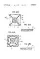
- FIG. 1A typical BGA semiconductor package is shown in FIG. 1.
- the semiconductor chip 30 of the typical BGA package 1'is mounted to the top surface of a PCB 20 by thermal conductive resin 33 such as silver containing epoxy.
- the above package 1'also includes a solder ball array which comprises a plurality of solder balls 40 welded to the bottom surface of the above PCB 20.
- a plurality of PTHs (plated through holes) 23are vertically formed on a chip mounting portion of the PCB 20. As well known to those skilled in the art, heat is generated from the semiconductor chip 30 during the operation of the package 1'.
- heat generated from the chip 30ordinarily passes through the chip's bottom surface, the thermal conductive resin 33, the PTHs 23 of the PCB's chip mounting portion and the solder balls 40 thereby being dissipated outside the package 1'.
- the above BGA package 1'has the following problem. That is, since the heat of the chip 30 passes through the chip's bottom surface, the thermal conductive resin 33, the PTHs 23 and the solder balls 40 which are made of different materials with different heat resistances, the above package 1' fails to achieve effective heat dissipation. Furthermore, multi-pin BGA semiconductor packages with an increased number of solder balls have recently been widely used in order to achieve the recent trend of high speed signal transmission. Such multi-pin BGA semiconductor packages must have an improved structure suitable for more effectively dissipating the chip's heat during the operation of the package. Therefore, BGA semiconductor packages with improved heat dissipation have been actively studied. The inventors of this invention have studied to provide a BGA semiconductor package with improved heat dissipation on the basis of a theory that about 60-70% of the chip's heat is dissipated through the chip's bottom surface.
- an object of the present inventionto provide a structurally improved BGA semiconductor package in which the above problems can be overcome and which enlarges the heat dissipating area of the chip's bottom surface by extending the edge of a chip mounting die paddle, formed of a copper or copper alloy layer, to the outside of the package and by mounting a ring-type heat sink, surrounding the encapsulant of the package, to the top surface of the extended portion of the above die paddle, thereby directly and effectively dissipating the chip's heat through the heat sink with high thermal conductivity.
- a BGA semiconductor packagein accordance with a preferred embodiment of the present invention comprises a semiconductor chip mounted on one side of a printed circuit board (PCB); the PCB having a chip mounting die paddle, the edge of the die paddle being partially extended to the edge of the package in order to form an extended portion exposed outside the package; a wire electrically connecting a bond pad of the chip to an electrical conductive trace of the PCB; an encapsulant encapsulating the chip and wire in order to protect the chip and wire from surroundings; a ring-type heat sink attached to the extended portion of the die paddle and surrounding the encapsulant; and a plurality of solder balls welded to the other side of the PCB and used as input and output terminals of the package.
- PCBprinted circuit board
- FIG. 1is a sectional view showing the construction of a typical BGA semiconductor package
- FIG. 2is a sectional view showing the construction of a BGA semiconductor package in accordance with a preferred embodiment of the present invention
- FIGS. 3a and 3bare views showing the construction of a PCB (printed circuit board) used in the BGA semiconductor package of the present invention, in which:
- FIG. 3ais a plan view of the PCB
- FIG. 3bis a sectional view of the PCB taken along the section line 3B--3B of FIG. 3a;
- FIGS. 4a and 4bare views showing the construction of a PCB in accordance with another embodiment of the present invention, in which:
- FIG. 4ais a plan view of the PCB
- FIG. 4bis a sectional view of the PCB taken along the section line 4B--4B of FIG. 4a;
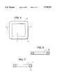
- FIG. 5is a plan view showing the construction of a ring-type heat sink used in the BGA semiconductor package of the present invention.
- FIG. 6is a sectional view of the heat sink taken along the section line 6--6 of FIG. 5;
- FIG. 7is a sectional showing the construction of a ring-type heat sink in accordance with another embodiment of the present invention.
- FIG. 2is a sectional view showing the construction of the BGA semiconductor package 1 in accordance with a preferred embodiment of the present invention.
- the semiconductor chip 30is mounted to the top surface of a chip mounting die paddle 21 of a PCB 20.
- the die paddle 21is formed on either side of the PCB 20. In the embodiment of FIG. 2, the die paddle 21 is formed on the top side of the PCB 20.
- Each side of the above PCB 20is coated with copper or copper alloy layer.
- the semiconductor chip 30is mounted to the PCB 20 using high thermal conductive resin 33 such as silver containing epoxy. of course, it should be understood that the PCB 20 may be substituted with another conventional circuit board.
- the above PCB 20is preferably formed of bismaleimide triazine.
- the electrical contact between the semiconductor chip 30 and PCB 20is achieved by wire bonding. That is, a plurality of bond pads (not shown) of the chip 30 are electrically connected to the electrical conductive trace 24 of the PCB 20 through a plurality of wires 31. The above trace is formed on the PCB 20.
- the semiconductor chip 30, wires 31 and selective peripheral elementsare encapsulated by an encapsulant 32 formed of encapsulating compound, for example, epoxy resin, thereby being protected from bad surroundings such as moisture, dust, external shock and vibration.
- the above resin encapsulant 32also relieves stress and strain caused by the relatively larger difference of thermal coefficient between the PCB 20 and chip 30.
- the encapsulant 32has another operation function in that it uniformly distributes stress and strain, which are concentrated to the corners of the chip 30, to the chip 30 thoroughly.
- a plurality of solder balls 40are welded to the bottom side of the PCB 20 thereby forming a solder ball array.
- the above solder balls 40act as input and output terminals of the package 1.
- the above package 1includes a ring-type heat sink 10 which surrounds the encapsulant 32.
- the heat sink 10has a generally rectangular configuration. However, it should be understood that there exist various different heat sink configurations which yield the same result as that of the above-described rectangular configuration without affecting the functioning of this invention.
- a plurality of conventional PTHs (plated through holes) 23are formed on the chip mounting portion of the PCB 20 in addition to the above ring-type heat sink 10.
- the BGA semiconductor packagemay be not provided with any PTH.
- the BGA semiconductor package with both the heat sink 10 and PTHs 23has further improved heat dissipating effect in comparison with the BGA package of this invention with no PTH.
- FIGS. 3a and 3bshow the construction of a PCB 20 according to an embodiment of this invention
- FIGS. 4a and 4bshow the construction of a PCB 20 according to another embodiment of this invention.
- FIG. 3ais a plan view of the PCB 20 according to the one embodiment, while FIG. 3b is a sectional view of the PCB 20 taken along the section line 3B--3B of FIG. 3a.
- the edge 22' of the chip mounting die paddle 21is partially extended to the edge portion of the package thereby forming a plurality of extended portions 22. That is, the corners of the paddle 21 are extended to the corners of the package thereby forming the extended portions 22 of the paddle 21.
- the extended portions 22When considering the package producing process, it is preferable to form the extended portions 22 by extending the corners of the paddle 21 to the corners of the package.
- the ring-type heat sink 10is mounted to the extended portions 22 of the paddle 21 such that the sink 10 surrounds the encapsulant 32.
- the above heat sink 10enlarges the heat dissipating area of the package as will be described later herein.
- the above die paddle 21 and its extended portions 22are formed of copper or copper alloy layer having a good heat transfer rate.
- the area (EA) inside the dash and dotis the encapsulating area which will be encapsulated with encapsulating compound to form the encapsulant 32.
- FIG. 3bshows the die paddle 21 and its extended portions 22 deposited on the PCB 20.
- the height of the die paddle 21 and its extended portions 22is lower than that of a solder mask 25 of FIG. 2.
- FIG. 4ais a plan view of the PCB 20 according to the other embodiment, while FIG. 4b is a sectional view of the PCB 20 taken along the section line 4B--4B of FIG. 4a.
- the edge of the chip mounting die paddle 21is partially extended to the edge of the package. That is, the paddle's corners are extended to the edge of the package thereby forming an integrated extended portion 22 covering all of the edge portion of the package.
- the heat dissipating effect of the package according to this embodimentis maximized.
- FIG. 4bshows the die paddle 21 and its extended portions 22 deposited on the PCB 20.
- FIGS. 5 and 6show the ring-type heat sink 10 according to an embodiment of this invention
- FIG. 7shows the ring-type heat sink 10 according to another embodiment of this invention
- the heat sink 10is mounted to the extended portion 22 of the die paddle 21 such that the heat sink 10 surrounds the encapsulant 32 outside the package.
- the above heat sink 10has a central opening 11.
- the opening 11is larger than the encapsulant 32, so the heat sink 10 is prevented from coming into direct contact with the encapsulant 32 which is formed of encapsulating compound.
- the stress and strain caused by the difference of thermal coefficient between the heat sink 10 and encapsulant 32may be increased to cause an operational error in the package.
- the bonding surface or bottom surface of the heat sink 10may be a flat surface as shown in FIG. 6.
- the bonding surface of the heat sink 10may be partially embossed in order to form embossments 12 as shown in FIG. 7.
- the heat sink 10 of FIG. 7is mounted to the paddle's extended portions 22 of FIG. 3a at the embossments 12.
- the heat sink 10is preferably formed of a metal such as copper, copper alloy, aluminum or stainless steel.
- a metalsuch as copper, copper alloy, aluminum or stainless steel.
- the radius of curvature of the each rounded corner 13is not less than 40 mil.
- the above heat sink 10may be attached to the extended portion 22 of the die paddle 21 using epoxy or bonding tape having good thermal conductivity.
- the heat sink 10may be attached to the extended portion 22 of the die paddle 21 through intermetallic welding.
- the heat sink 10may be attached to the extended portion 22 of the die paddle 21 through soldering with an Sn/Pb containing solder. In the case of use of the above solder, the bonding strength between the heat sink 10 and extended portion 22 is further increased.
- the heat sink 10may be anodized to form a thin film on the heat sink's surface in order to protect the heat sink's surface.
- the surface of the heat sink 10may be treated with nickel or chrome.
- the edge of the chip mounting die paddle 21 formed of copper or copper alloyis partially extended to the edge of the package in order to form the extended portion 22.
- the heat sink 10is attached to the top surface of the above extended portion 22 of the die paddle 21 and exposed outside the package.
- the BGA package with both the heat sink 10 and PTHs 23 according to the preferred embodiment of this inventionfurther improves the heat dissipating effect.
- the present inventionprovides a BGA semiconductor package with a ring-type heat sink. Since the heat sink is totally exposed outside the encapsulant of the package, heat generated from the chip is effectively dissipated outside the package.
- a plurality of plated through holes (PTH)may be formed on the chip mounting portion of the PCB.
- PTHplated through holes
- the BGA package of this inventionimproves the operational performance and lengthens the expected life span of the package. Another advantage of the above BGA package is resided in that the package prevents operational error while the semiconductor chip is being operated.
Landscapes
- Engineering & Computer Science (AREA)
- Microelectronics & Electronic Packaging (AREA)
- Physics & Mathematics (AREA)
- Condensed Matter Physics & Semiconductors (AREA)
- General Physics & Mathematics (AREA)
- Computer Hardware Design (AREA)
- Power Engineering (AREA)
- Chemical & Material Sciences (AREA)
- Materials Engineering (AREA)
- Cooling Or The Like Of Semiconductors Or Solid State Devices (AREA)
Abstract
Description
Claims (8)
Applications Claiming Priority (2)
| Application Number | Priority Date | Filing Date | Title |
|---|---|---|---|
| KR95-41438 | 1995-11-15 | ||
| KR1019950041438AKR100201380B1 (en) | 1995-11-15 | 1995-11-15 | Heat Dissipation Structure of BGA Semiconductor Package |
Publications (1)
| Publication Number | Publication Date |
|---|---|
| US5708567Atrue US5708567A (en) | 1998-01-13 |
Family
ID=19434174
Family Applications (1)
| Application Number | Title | Priority Date | Filing Date |
|---|---|---|---|
| US08/748,937Expired - LifetimeUS5708567A (en) | 1995-11-15 | 1996-11-13 | Ball grid array semiconductor package with ring-type heat sink |
Country Status (3)
| Country | Link |
|---|---|
| US (1) | US5708567A (en) |
| JP (1) | JP2881575B2 (en) |
| KR (1) | KR100201380B1 (en) |
Cited By (46)
| Publication number | Priority date | Publication date | Assignee | Title |
|---|---|---|---|---|
| US5889324A (en)* | 1998-03-30 | 1999-03-30 | Nec Corporation | Package for a semiconductor device |
| KR19990045687A (en)* | 1997-11-28 | 1999-06-25 | 이데이 노부유끼 | Semiconductor device, manufacturing method thereof and electronic device using same |
| US5929514A (en)* | 1998-05-26 | 1999-07-27 | Analog Devices, Inc. | Thermally enhanced lead-under-paddle I.C. leadframe |
| US5963792A (en)* | 1998-02-05 | 1999-10-05 | Micron Technology, Inc. | Use of an oxide surface to facilitate gate break on a carrier substrate for a semiconductor device |
| US5985695A (en)* | 1996-04-24 | 1999-11-16 | Amkor Technology, Inc. | Method of making a molded flex circuit ball grid array |
| US6052045A (en)* | 1999-03-12 | 2000-04-18 | Kearney-National, Inc. | Electromechanical switching device package with controlled impedance environment |
| US6060775A (en)* | 1996-07-30 | 2000-05-09 | Texas Instruments Incorporated | Semiconductor device |
| US6061242A (en)* | 1999-02-25 | 2000-05-09 | Micron Technology, Inc. | Die paddle heat sink with thermal posts |
| US6060778A (en)* | 1997-05-17 | 2000-05-09 | Hyundai Electronics Industries Co. Ltd. | Ball grid array package |
| US6081429A (en)* | 1999-01-20 | 2000-06-27 | Micron Technology, Inc. | Test interposer for use with ball grid array packages assemblies and ball grid array packages including same and methods |
| US6084297A (en)* | 1998-09-03 | 2000-07-04 | Micron Technology, Inc. | Cavity ball grid array apparatus |
| US6097089A (en)* | 1998-01-28 | 2000-08-01 | Mitsubishi Gas Chemical Company, Inc. | Semiconductor plastic package, metal plate for said package, and method of producing copper-clad board for said package |
| US6121686A (en)* | 1996-08-13 | 2000-09-19 | Sony Corporation | Ball grid array package having through-holes disposed in the substrate under the chip |
| US6163956A (en)* | 1998-02-23 | 2000-12-26 | Micron Technology, Inc. | Method of making chip scale package with heat spreade |
| DE19960246A1 (en)* | 1999-12-14 | 2001-07-05 | Infineon Technologies Ag | Housing arrangement of a semiconductor device |
| US6285561B1 (en)* | 1998-12-18 | 2001-09-04 | U.S. Philips Corporation | Data carrier module device having integrated circuit and transmission coil connection contacts covered by a common protective cap |
| US6392286B1 (en) | 1999-08-02 | 2002-05-21 | Samsung Electronics Co., Ltd. | Semiconductor chip packaging system and a semiconductor chip packaging method using the same |
| US6399417B1 (en)* | 2001-03-06 | 2002-06-04 | Siliconware Precision Industries Co., Ltd. | Method of fabricating plated circuit lines over ball grid array substrate |
| US6404067B1 (en) | 1998-06-01 | 2002-06-11 | Intel Corporation | Plastic ball grid array package with improved moisture resistance |
| US6404059B1 (en)* | 2000-02-08 | 2002-06-11 | Mitsubishi Denki Kabushiki Kaisha | Semiconductor device having a mounting structure and fabrication method thereof |
| US6410977B1 (en)* | 1997-12-12 | 2002-06-25 | Seiko Epson Corporation | Semiconductor device, circuit board electronic instrument and method of making a semiconductor device |
| US6429513B1 (en) | 2001-05-25 | 2002-08-06 | Amkor Technology, Inc. | Active heat sink for cooling a semiconductor chip |
| US6432751B1 (en)* | 1997-04-11 | 2002-08-13 | Matsushita Electric Industrial Co., Ltd. | Resin mold electric part and producing method therefor |
| GB2373924A (en)* | 1997-05-17 | 2002-10-02 | Hyundai Electronics Ind | IC device with a metal thermal conductive layer having an opening for evacuating air |
| US20020179327A1 (en)* | 2001-05-30 | 2002-12-05 | Chihiro Araki | Semiconductor chip soldering land pattern |
| US20030011064A1 (en)* | 2001-07-11 | 2003-01-16 | Combs Edward G. | Enhanced thermal dissipation integrated circuit package and method of manufacturing enhanced thermal dissipation integrated circuit package |
| RU2199794C2 (en)* | 1999-12-20 | 2003-02-27 | Хитачи, Лтд. | Insulation printed circuit board and high-power semiconductor device employing it |
| US20030080402A1 (en)* | 1998-02-23 | 2003-05-01 | Corisis David J. | Chip scale package with heat spreader and method of manufacture |
| US6566761B1 (en)* | 2002-05-03 | 2003-05-20 | Applied Micro Circuits Corporation | Electronic device package with high speed signal interconnect between die pad and external substrate pad |
| US6566164B1 (en) | 2000-12-07 | 2003-05-20 | Amkor Technology, Inc. | Exposed copper strap in a semiconductor package |
| US20030169138A1 (en)* | 2002-03-08 | 2003-09-11 | Motta James J. | Surface mount molded relay package and method of manufacturing same |
| US20030178719A1 (en)* | 2002-03-22 | 2003-09-25 | Combs Edward G. | Enhanced thermal dissipation integrated circuit package and method of manufacturing enhanced thermal dissipation integrated circuit package |
| USRE38381E1 (en) | 2000-07-21 | 2004-01-13 | Kearney-National Inc. | Inverted board mounted electromechanical device |
| US20050003585A1 (en)* | 2001-07-11 | 2005-01-06 | Combs Edward G. | Method of manufacturing an enhanced thermal dissipation integrated circuit package |
| US20050085011A1 (en)* | 2003-10-15 | 2005-04-21 | Tsung-Hung Lee | Thermally enhanced packaging structure and fabrication method thereof |
| US6919631B1 (en) | 2001-12-07 | 2005-07-19 | Amkor Technology, Inc. | Structures for improving heat dissipation in stacked semiconductor packages |
| US20060286711A1 (en)* | 2005-06-06 | 2006-12-21 | Triquint Semiconductor, Inc. | Signal isolation in a package substrate |
| US20080106624A1 (en)* | 1999-12-08 | 2008-05-08 | Amkor Technology, Inc. | Method of using a camera module |
| US20080277800A1 (en)* | 2007-05-08 | 2008-11-13 | Samsung Electronics Co., Ltd. | Semiconductor package and method of forming the same |
| US20090039488A1 (en)* | 2007-08-10 | 2009-02-12 | Siliconware Precision Industries Co., Ltd. | Semiconductor package and method for fabricating the same |
| US20100006332A1 (en)* | 2007-02-09 | 2010-01-14 | Panasonic Corporation | Circuit board, laminating circuit board and electronic apparatus |
| US20100277921A1 (en)* | 2009-05-01 | 2010-11-04 | Daniel Sekowski | Electronic Apparatus |
| US20100327439A1 (en)* | 2007-05-08 | 2010-12-30 | Tae-Joo Hwang | Semiconductor package and method of forming the same |
| US9147600B2 (en) | 2013-01-03 | 2015-09-29 | Infineon Technologies Ag | Packages for multiple semiconductor chips |
| US9437517B2 (en) | 2013-01-07 | 2016-09-06 | Panasonic Corporation | Semiconductor apparatus including a heat dissipating member |
| US20180332699A1 (en)* | 2017-02-21 | 2018-11-15 | Unlimiter Mfa Co., Ltd. | Printed circuit board |
Families Citing this family (6)
| Publication number | Priority date | Publication date | Assignee | Title |
|---|---|---|---|---|
| KR100604329B1 (en)* | 1999-04-13 | 2006-07-24 | 삼성테크윈 주식회사 | IC card integrated circuit assembly |
| JP2008060172A (en)* | 2006-08-29 | 2008-03-13 | Toshiba Corp | Semiconductor device |
| JP5017977B2 (en)* | 2006-09-14 | 2012-09-05 | 富士通セミコンダクター株式会社 | Semiconductor device and manufacturing method thereof |
| KR100802393B1 (en) | 2007-02-15 | 2008-02-13 | 삼성전기주식회사 | Package board and its manufacturing method |
| KR101311707B1 (en)* | 2013-03-26 | 2013-09-25 | 주식회사 심텍 | Die stack package and method for fabricating the same |
| CN111370378B (en)* | 2020-03-17 | 2022-08-05 | 电子科技大学 | Chip radiator |
Citations (7)
| Publication number | Priority date | Publication date | Assignee | Title |
|---|---|---|---|---|
| US4809053A (en)* | 1986-08-12 | 1989-02-28 | Shinko Electric Industries Co., Ltd. | Semiconductor device and lead frame used therefor |
| US5371404A (en)* | 1993-02-04 | 1994-12-06 | Motorola, Inc. | Thermally conductive integrated circuit package with radio frequency shielding |
| US5442234A (en)* | 1992-09-10 | 1995-08-15 | Vlsi Technology, Inc. | Apparatus for thermally coupling a heat sink to a leadframe |
| US5485037A (en)* | 1993-04-12 | 1996-01-16 | Amkor Electronics, Inc. | Semiconductor device having a thermal dissipator and electromagnetic shielding |
| US5532905A (en)* | 1994-07-19 | 1996-07-02 | Analog Devices, Inc. | Thermally enhanced leadframe for packages that utilize a large number of leads |
| US5586007A (en)* | 1993-02-24 | 1996-12-17 | Fuji Xerox Co., Ltd. | Circuit board having improved thermal radiation |
| US5598321A (en)* | 1995-09-11 | 1997-01-28 | National Semiconductor Corporation | Ball grid array with heat sink |
Family Cites Families (2)
| Publication number | Priority date | Publication date | Assignee | Title |
|---|---|---|---|---|
| JP2599497Y2 (en)* | 1993-06-25 | 1999-09-06 | 美津濃株式会社 | Golf club head |
| JPH07142627A (en)* | 1993-11-18 | 1995-06-02 | Fujitsu Ltd | Semiconductor device and manufacturing method thereof |
- 1995
- 1995-11-15KRKR1019950041438Apatent/KR100201380B1/ennot_activeExpired - Lifetime
- 1996
- 1996-06-24JPJP8182798Apatent/JP2881575B2/ennot_activeExpired - Fee Related
- 1996-11-13USUS08/748,937patent/US5708567A/ennot_activeExpired - Lifetime
Patent Citations (7)
| Publication number | Priority date | Publication date | Assignee | Title |
|---|---|---|---|---|
| US4809053A (en)* | 1986-08-12 | 1989-02-28 | Shinko Electric Industries Co., Ltd. | Semiconductor device and lead frame used therefor |
| US5442234A (en)* | 1992-09-10 | 1995-08-15 | Vlsi Technology, Inc. | Apparatus for thermally coupling a heat sink to a leadframe |
| US5371404A (en)* | 1993-02-04 | 1994-12-06 | Motorola, Inc. | Thermally conductive integrated circuit package with radio frequency shielding |
| US5586007A (en)* | 1993-02-24 | 1996-12-17 | Fuji Xerox Co., Ltd. | Circuit board having improved thermal radiation |
| US5485037A (en)* | 1993-04-12 | 1996-01-16 | Amkor Electronics, Inc. | Semiconductor device having a thermal dissipator and electromagnetic shielding |
| US5532905A (en)* | 1994-07-19 | 1996-07-02 | Analog Devices, Inc. | Thermally enhanced leadframe for packages that utilize a large number of leads |
| US5598321A (en)* | 1995-09-11 | 1997-01-28 | National Semiconductor Corporation | Ball grid array with heat sink |
Cited By (95)
| Publication number | Priority date | Publication date | Assignee | Title |
|---|---|---|---|---|
| US6265767B1 (en) | 1919-04-03 | 2001-07-24 | Mitsubishi Gas Chemical Company, Inc. | Semiconductor plastic package, metal plate for said package, and method of producing copper-clad board for said package |
| US5985695A (en)* | 1996-04-24 | 1999-11-16 | Amkor Technology, Inc. | Method of making a molded flex circuit ball grid array |
| US6124637A (en)* | 1996-04-24 | 2000-09-26 | Amkor Technology, Inc. | Carrier strip and molded flex circuit ball grid array and method of making |
| US6060775A (en)* | 1996-07-30 | 2000-05-09 | Texas Instruments Incorporated | Semiconductor device |
| US6121686A (en)* | 1996-08-13 | 2000-09-19 | Sony Corporation | Ball grid array package having through-holes disposed in the substrate under the chip |
| US6432751B1 (en)* | 1997-04-11 | 2002-08-13 | Matsushita Electric Industrial Co., Ltd. | Resin mold electric part and producing method therefor |
| GB2325340B (en)* | 1997-05-17 | 2002-09-11 | Hyundai Electronics Ind | Ball grid array package |
| GB2373924A (en)* | 1997-05-17 | 2002-10-02 | Hyundai Electronics Ind | IC device with a metal thermal conductive layer having an opening for evacuating air |
| US6060778A (en)* | 1997-05-17 | 2000-05-09 | Hyundai Electronics Industries Co. Ltd. | Ball grid array package |
| GB2373924B (en)* | 1997-05-17 | 2002-11-13 | Hyundai Electronics Ind | Ball grid array package |
| KR19990045687A (en)* | 1997-11-28 | 1999-06-25 | 이데이 노부유끼 | Semiconductor device, manufacturing method thereof and electronic device using same |
| US6514847B1 (en) | 1997-11-28 | 2003-02-04 | Sony Corporation | Method for making a semiconductor device |
| US6410977B1 (en)* | 1997-12-12 | 2002-06-25 | Seiko Epson Corporation | Semiconductor device, circuit board electronic instrument and method of making a semiconductor device |
| US6097089A (en)* | 1998-01-28 | 2000-08-01 | Mitsubishi Gas Chemical Company, Inc. | Semiconductor plastic package, metal plate for said package, and method of producing copper-clad board for said package |
| US6251702B1 (en) | 1998-02-05 | 2001-06-26 | Micron Technology, Inc. | Use of an oxide surface to facilitate gate break on a carrier substrate for a semiconductor device |
| US6545368B2 (en) | 1998-02-05 | 2003-04-08 | Micron Technology, Inc. | Use of an oxide surface to facilitate gate break on a carrier substrate for a semiconductor device |
| US5969427A (en)* | 1998-02-05 | 1999-10-19 | Micron Technology, Inc. | Use of an oxide surface to facilitate gate break on a carrier substrate for a semiconductor device |
| US5963792A (en)* | 1998-02-05 | 1999-10-05 | Micron Technology, Inc. | Use of an oxide surface to facilitate gate break on a carrier substrate for a semiconductor device |
| US6404069B2 (en) | 1998-02-05 | 2002-06-11 | Micron Technology, Inc. | Use of oxide surface to facilitate gate break on a carrier substrate for a semiconductor device |
| US20050248038A1 (en)* | 1998-02-23 | 2005-11-10 | Corisis David J | Chip scale package with heat spreader |
| US6314639B1 (en)* | 1998-02-23 | 2001-11-13 | Micron Technology, Inc. | Chip scale package with heat spreader and method of manufacture |
| US6505400B1 (en) | 1998-02-23 | 2003-01-14 | Micron Technology, Inc. | Method of making chip scale package with heat spreader |
| US6735859B2 (en) | 1998-02-23 | 2004-05-18 | Micron Technology, Inc. | Method of manufacturing chip scale package |
| US20060186533A1 (en)* | 1998-02-23 | 2006-08-24 | Corisis David J | Chip scale package with heat spreader |
| US6163956A (en)* | 1998-02-23 | 2000-12-26 | Micron Technology, Inc. | Method of making chip scale package with heat spreade |
| US20030080402A1 (en)* | 1998-02-23 | 2003-05-01 | Corisis David J. | Chip scale package with heat spreader and method of manufacture |
| US7233056B1 (en) | 1998-02-23 | 2007-06-19 | Micron Technology, Inc. | Chip scale package with heat spreader |
| US7312516B2 (en) | 1998-02-23 | 2007-12-25 | Micron Technology, Inc. | Chip scale package with heat spreader |
| US5889324A (en)* | 1998-03-30 | 1999-03-30 | Nec Corporation | Package for a semiconductor device |
| US5929514A (en)* | 1998-05-26 | 1999-07-27 | Analog Devices, Inc. | Thermally enhanced lead-under-paddle I.C. leadframe |
| US6404067B1 (en) | 1998-06-01 | 2002-06-11 | Intel Corporation | Plastic ball grid array package with improved moisture resistance |
| US6084297A (en)* | 1998-09-03 | 2000-07-04 | Micron Technology, Inc. | Cavity ball grid array apparatus |
| US7268013B2 (en) | 1998-09-03 | 2007-09-11 | Micron Technology, Inc. | Method of fabricating a semiconductor die package having improved inductance characteristics |
| US6326244B1 (en) | 1998-09-03 | 2001-12-04 | Micron Technology, Inc. | Method of making a cavity ball grid array apparatus |
| US20070007517A1 (en)* | 1998-09-03 | 2007-01-11 | Brooks Jerry M | Cavity ball grid array apparatus having improved inductance characteristics |
| US20060055040A1 (en)* | 1998-09-03 | 2006-03-16 | Brooks Jerry M | Cavity ball grid array apparatus having improved inductance characteristics |
| US6982486B2 (en) | 1998-09-03 | 2006-01-03 | Micron Technology, Inc. | Cavity ball grid array apparatus having improved inductance characteristics and method of fabricating the same |
| US20040207064A1 (en)* | 1998-09-03 | 2004-10-21 | Brooks Jerry M. | Cavity ball grid array apparatus having improved inductance characteristics |
| US6740971B2 (en)* | 1998-09-03 | 2004-05-25 | Micron Technology, Inc. | Cavity ball grid array apparatus having improved inductance characteristics |
| US6285561B1 (en)* | 1998-12-18 | 2001-09-04 | U.S. Philips Corporation | Data carrier module device having integrated circuit and transmission coil connection contacts covered by a common protective cap |
| US6081429A (en)* | 1999-01-20 | 2000-06-27 | Micron Technology, Inc. | Test interposer for use with ball grid array packages assemblies and ball grid array packages including same and methods |
| US6452807B1 (en) | 1999-01-20 | 2002-09-17 | Micron Technology, Inc. | Test interposer for use with ball grid array packages, assemblies and ball grid array packages including same, and methods |
| US6061242A (en)* | 1999-02-25 | 2000-05-09 | Micron Technology, Inc. | Die paddle heat sink with thermal posts |
| US6052045A (en)* | 1999-03-12 | 2000-04-18 | Kearney-National, Inc. | Electromechanical switching device package with controlled impedance environment |
| US6392286B1 (en) | 1999-08-02 | 2002-05-21 | Samsung Electronics Co., Ltd. | Semiconductor chip packaging system and a semiconductor chip packaging method using the same |
| US20110115918A1 (en)* | 1999-12-08 | 2011-05-19 | Amkor Technology, Inc. | Camera module having lens mount with ir filter |
| US9332164B2 (en) | 1999-12-08 | 2016-05-03 | Amkor Technology, Inc. | Molded semiconductor package with snap lid |
| US8994860B2 (en) | 1999-12-08 | 2015-03-31 | Amkor, Technology, Inc. | Molded image sensor package and method |
| US20080106624A1 (en)* | 1999-12-08 | 2008-05-08 | Amkor Technology, Inc. | Method of using a camera module |
| US9735191B2 (en) | 1999-12-08 | 2017-08-15 | Amkor Technology, Inc. | Molded semiconductor package |
| US7208827B2 (en) | 1999-12-14 | 2007-04-24 | Infineon Technologies Ag | Encasing arrangement for a semiconductor component |
| DE19960246A1 (en)* | 1999-12-14 | 2001-07-05 | Infineon Technologies Ag | Housing arrangement of a semiconductor device |
| US20050040517A1 (en)* | 1999-12-14 | 2005-02-24 | Christian Hauser | Encasing arrangement for a semicoductor component |
| RU2199794C2 (en)* | 1999-12-20 | 2003-02-27 | Хитачи, Лтд. | Insulation printed circuit board and high-power semiconductor device employing it |
| US6404059B1 (en)* | 2000-02-08 | 2002-06-11 | Mitsubishi Denki Kabushiki Kaisha | Semiconductor device having a mounting structure and fabrication method thereof |
| USRE38381E1 (en) | 2000-07-21 | 2004-01-13 | Kearney-National Inc. | Inverted board mounted electromechanical device |
| US6566164B1 (en) | 2000-12-07 | 2003-05-20 | Amkor Technology, Inc. | Exposed copper strap in a semiconductor package |
| US6723582B2 (en) | 2000-12-07 | 2004-04-20 | Amkor Technology, Inc. | Method of making a semiconductor package having exposed metal strap |
| US6399417B1 (en)* | 2001-03-06 | 2002-06-04 | Siliconware Precision Industries Co., Ltd. | Method of fabricating plated circuit lines over ball grid array substrate |
| US6429513B1 (en) | 2001-05-25 | 2002-08-06 | Amkor Technology, Inc. | Active heat sink for cooling a semiconductor chip |
| US6841887B2 (en)* | 2001-05-30 | 2005-01-11 | Kabushiki Kaisha Moric | Semiconductor chip soldering land pattern |
| US20020179327A1 (en)* | 2001-05-30 | 2002-12-05 | Chihiro Araki | Semiconductor chip soldering land pattern |
| US20050003585A1 (en)* | 2001-07-11 | 2005-01-06 | Combs Edward G. | Method of manufacturing an enhanced thermal dissipation integrated circuit package |
| US6734552B2 (en) | 2001-07-11 | 2004-05-11 | Asat Limited | Enhanced thermal dissipation integrated circuit package |
| US20030011064A1 (en)* | 2001-07-11 | 2003-01-16 | Combs Edward G. | Enhanced thermal dissipation integrated circuit package and method of manufacturing enhanced thermal dissipation integrated circuit package |
| US7015072B2 (en) | 2001-07-11 | 2006-03-21 | Asat Limited | Method of manufacturing an enhanced thermal dissipation integrated circuit package |
| US6919631B1 (en) | 2001-12-07 | 2005-07-19 | Amkor Technology, Inc. | Structures for improving heat dissipation in stacked semiconductor packages |
| US20030169138A1 (en)* | 2002-03-08 | 2003-09-11 | Motta James J. | Surface mount molded relay package and method of manufacturing same |
| US20030178719A1 (en)* | 2002-03-22 | 2003-09-25 | Combs Edward G. | Enhanced thermal dissipation integrated circuit package and method of manufacturing enhanced thermal dissipation integrated circuit package |
| US20040046241A1 (en)* | 2002-03-22 | 2004-03-11 | Combs Edward G. | Method of manufacturing enhanced thermal dissipation integrated circuit package |
| US6566761B1 (en)* | 2002-05-03 | 2003-05-20 | Applied Micro Circuits Corporation | Electronic device package with high speed signal interconnect between die pad and external substrate pad |
| US20050085011A1 (en)* | 2003-10-15 | 2005-04-21 | Tsung-Hung Lee | Thermally enhanced packaging structure and fabrication method thereof |
| US6989293B2 (en)* | 2003-10-15 | 2006-01-24 | Benq Corporation | Thermally enhanced packaging structure and fabrication method thereof |
| US20060286711A1 (en)* | 2005-06-06 | 2006-12-21 | Triquint Semiconductor, Inc. | Signal isolation in a package substrate |
| US7250673B2 (en)* | 2005-06-06 | 2007-07-31 | Triquint Semiconductor, Inc. | Signal isolation in a package substrate |
| US20100006332A1 (en)* | 2007-02-09 | 2010-01-14 | Panasonic Corporation | Circuit board, laminating circuit board and electronic apparatus |
| US20100327439A1 (en)* | 2007-05-08 | 2010-12-30 | Tae-Joo Hwang | Semiconductor package and method of forming the same |
| US8022555B2 (en)* | 2007-05-08 | 2011-09-20 | Samsung Electronics Co., Ltd. | Semiconductor package and method of forming the same |
| US8129221B2 (en) | 2007-05-08 | 2012-03-06 | Samsung Electronics Co., Ltd. | Semiconductor package and method of forming the same |
| US9685400B2 (en) | 2007-05-08 | 2017-06-20 | Samsung Electronics Co., Ltd. | Semiconductor package and method of forming the same |
| US8421244B2 (en) | 2007-05-08 | 2013-04-16 | Samsung Electronics Co., Ltd. | Semiconductor package and method of forming the same |
| US8736035B2 (en) | 2007-05-08 | 2014-05-27 | Samsung Electronics Co. Ltd. | Semiconductor package and method of forming the same |
| US9484292B2 (en) | 2007-05-08 | 2016-11-01 | Samsung Electronics Co. Ltd. | Semiconductor package and method of forming the same |
| US20080277800A1 (en)* | 2007-05-08 | 2008-11-13 | Samsung Electronics Co., Ltd. | Semiconductor package and method of forming the same |
| US20090039488A1 (en)* | 2007-08-10 | 2009-02-12 | Siliconware Precision Industries Co., Ltd. | Semiconductor package and method for fabricating the same |
| US20140080264A1 (en)* | 2007-08-10 | 2014-03-20 | Siliconware Precision Industries Co., Ltd | Method for fabricating leadframe-based semiconductor package |
| US8618641B2 (en)* | 2007-08-10 | 2013-12-31 | Siliconware Precision Industries Co., Ltd | Leadframe-based semiconductor package |
| US9130064B2 (en)* | 2007-08-10 | 2015-09-08 | Siliconware Precision Industries Co., Ltd. | Method for fabricating leadframe-based semiconductor package with connecting pads top and bottom surfaces of carrier |
| US20130236995A1 (en)* | 2009-05-01 | 2013-09-12 | Vossloh-Schwabe Optoelectronic Gmbh & Co. Kg | Electronic apparatus having an encapsulating layer within and outside of a molded frame overlying a connection arrangement on a circuit board |
| US9105819B2 (en)* | 2009-05-01 | 2015-08-11 | Abl Ip Holding Llc | Method for making an electronic apparatus having an encapsulating layer within and outside of a molded frame overlying a connection arrangement on a circuit board |
| US8184440B2 (en)* | 2009-05-01 | 2012-05-22 | Abl Ip Holding Llc | Electronic apparatus having an encapsulating layer within and outside of a molded frame overlying a connection arrangement on a circuit board |
| US20100277921A1 (en)* | 2009-05-01 | 2010-11-04 | Daniel Sekowski | Electronic Apparatus |
| US9147600B2 (en) | 2013-01-03 | 2015-09-29 | Infineon Technologies Ag | Packages for multiple semiconductor chips |
| US9437517B2 (en) | 2013-01-07 | 2016-09-06 | Panasonic Corporation | Semiconductor apparatus including a heat dissipating member |
| US20180332699A1 (en)* | 2017-02-21 | 2018-11-15 | Unlimiter Mfa Co., Ltd. | Printed circuit board |
Also Published As
| Publication number | Publication date |
|---|---|
| JPH10308466A (en) | 1998-11-17 |
| JP2881575B2 (en) | 1999-04-12 |
| KR100201380B1 (en) | 1999-06-15 |
| KR970030690A (en) | 1997-06-26 |
Similar Documents
| Publication | Publication Date | Title |
|---|---|---|
| US5708567A (en) | Ball grid array semiconductor package with ring-type heat sink | |
| EP1374305B1 (en) | Enhanced die-down ball grid array and method for making the same | |
| US5953589A (en) | Ball grid array semiconductor package with solder balls fused on printed circuit board and method for fabricating the same | |
| US6404049B1 (en) | Semiconductor device, manufacturing method thereof and mounting board | |
| US6865084B2 (en) | Thermally enhanced semiconductor package with EMI shielding | |
| JP3437369B2 (en) | Chip carrier and semiconductor device using the same | |
| US5583377A (en) | Pad array semiconductor device having a heat sink with die receiving cavity | |
| US20050236701A1 (en) | Leadframe, plastic-encapsulated semiconductor device, and method for fabricating the same | |
| CA2166925A1 (en) | Thin packaging of multi-chip modules with enhanced thermal/power management | |
| JPH06349893A (en) | Flip chip connection semiconductor package | |
| JPH03174749A (en) | semiconductor equipment | |
| KR100203932B1 (en) | BGA package having thermal emissive substrate attached to chip | |
| JP2852112B2 (en) | Semiconductor integrated circuit device | |
| KR100218633B1 (en) | Ball Grid Array Semiconductor Package with Carrier Frame | |
| KR100260996B1 (en) | Array type semiconductor package using a lead frame and its manufacturing method | |
| KR200172710Y1 (en) | Chip size package | |
| JP3016380B2 (en) | Semiconductor device | |
| JP2507627B2 (en) | Semiconductor device | |
| KR100225236B1 (en) | Ball Grid Array (BGA) Semiconductor Package | |
| KR19990056764A (en) | Ball grid array package | |
| KR19980025878A (en) | Ball grid array package with a heat sink attached to the chip | |
| JPH11111883A (en) | Semiconductor device | |
| KR200316720Y1 (en) | Ball grid array package | |
| KR20000001487A (en) | Ball grid array package having super-heat emission characteristic | |
| JPH10209322A (en) | Semiconductor device and its mounting structure |
Legal Events
| Date | Code | Title | Description |
|---|---|---|---|
| AS | Assignment | Owner name:ANAM INDUSTRIAL CO., LTD., KOREA, REPUBLIC OF Free format text:ASSIGNMENT OF ASSIGNORS INTEREST;ASSIGNORS:SHIM, IL KWON;HEO, YOUNG WOOK;REEL/FRAME:008315/0307 Effective date:19960508 Owner name:AMKOR ELECTRONICS, INC., ARIZONA Free format text:ASSIGNMENT OF ASSIGNORS INTEREST;ASSIGNORS:SHIM, IL KWON;HEO, YOUNG WOOK;REEL/FRAME:008315/0307 Effective date:19960508 | |
| STCF | Information on status: patent grant | Free format text:PATENTED CASE | |
| AS | Assignment | Owner name:ANAM SEMICONDUCTOR INC., KOREA, REPUBLIC OF Free format text:CHANGE OF NAME;ASSIGNORS:ANAM INDUSTRIAL CO., LTD.;AMKOR ELECTRONICS, INC.;REEL/FRAME:009586/0573;SIGNING DATES FROM 19980320 TO 19980414 Owner name:AMKOR TECHNOLOGY, INC., ARIZONA Free format text:CHANGE OF NAME;ASSIGNORS:ANAM INDUSTRIAL CO., LTD.;AMKOR ELECTRONICS, INC.;REEL/FRAME:009586/0573;SIGNING DATES FROM 19980320 TO 19980414 | |
| AS | Assignment | Owner name:GUARDIAN ASSETS, INC., PENNSYLVANIA Free format text:SECURITY INTEREST;ASSIGNOR:AMKOR TECHNOLOGY, INC.;REEL/FRAME:011122/0773 Effective date:20000428 | |
| AS | Assignment | Owner name:SOCIETE GENERALE, NEW YORK Free format text:RE-RECORD TO CORRECT RECEIVING PARTY NAME ON A DOCUMENT PREVIOUSLY RECORDED ON REEL 011122, FRAME 0773.;ASSIGNORS:AMKOR TECHNOLOGY, INC.;GUARDIAN ASSETS, INC.;REEL/FRAME:011457/0702 Effective date:20000428 | |
| AS | Assignment | Owner name:CITICORP USA, INC., NEW YORK Free format text:SECURITY INTEREST;ASSIGNORS:SOCIETE GENERALE;GUARDIAN ASSETS, INC.;REEL/FRAME:011682/0416 Effective date:20010330 | |
| FPAY | Fee payment | Year of fee payment:4 | |
| AS | Assignment | Owner name:AMKOR TECHNOLOGY KOREA, INC., KOREA, REPUBLIC OF Free format text:ASSIGNMENT OF ASSIGNORS INTEREST;ASSIGNOR:ANAM SEMICONDUCTOR, INC.;REEL/FRAME:013193/0683 Effective date:20000502 | |
| AS | Assignment | Owner name:AMKOR TECHNOLOGY, INC., ARIZONA Free format text:ASSIGNMENT OF ASSIGNORS INTEREST;ASSIGNOR:AMKOR TECHNOLOGY KOREA, INC.;REEL/FRAME:013323/0853 Effective date:20020913 | |
| AS | Assignment | Owner name:CITICORP NORTH AMERICA, INC. AS ADMINISTRATIVE AGE Free format text:SECURITY AGREEMENT;ASSIGNORS:AMKOR TECHNOLOGY, INC.;GUARDIAN ASSETS, INC.;REEL/FRAME:014885/0691 Effective date:20040629 | |
| AS | Assignment | Owner name:AMKOR TECHNOLOGY, INC., PENNSYLVANIA Free format text:RELEASE OF LIEN ON PATENTS;ASSIGNOR:CITICORP USA, INC. AS COLLATERAL AGENT;REEL/FRAME:015603/0572 Effective date:20040629 | |
| AS | Assignment | Owner name:CITICORP NORTH AMERICA, INC. AS "AGENT", NEW YORK Free format text:SECURITY AGREEMENT;ASSIGNORS:AMKOR TECHNOLOGY, INC.;GUARDIAN ASSETS, INC.;REEL/FRAME:015942/0521 Effective date:20041027 | |
| FPAY | Fee payment | Year of fee payment:8 | |
| AS | Assignment | Owner name:AMKOR TECHNOLOGY, INC., ARIZONA Free format text:TERMINATION & RELEASE OF PATENT SECURITY AGREEMENT;ASSIGNOR:CITICORP NORTH AMERICA, INC.;REEL/FRAME:017388/0868 Effective date:20051128 Owner name:BANK OF AMERICA, N.A., TEXAS Free format text:SECURITY AGREEMENT;ASSIGNOR:AMKOR TECHNOLOGY, INC.;REEL/FRAME:017379/0630 Effective date:20051123 | |
| FPAY | Fee payment | Year of fee payment:12 | |
| AS | Assignment | Owner name:BANK OF AMERICA, N.A., AS AGENT, CALIFORNIA Free format text:SECURITY INTEREST;ASSIGNOR:AMKOR TECHNOLOGY, INC.;REEL/FRAME:046683/0139 Effective date:20180713 | |
| AS | Assignment | Owner name:AMKOR TECHNOLOGY SINGAPORE HOLDING PTE.LTD., SINGAPORE Free format text:ASSIGNMENT OF ASSIGNORS INTEREST;ASSIGNOR:AMKOR TECHNOLOGY, INC.;REEL/FRAME:054036/0599 Effective date:20191119 |