US5708419A - Method of wire bonding an integrated circuit to an ultraflexible substrate - Google Patents
Method of wire bonding an integrated circuit to an ultraflexible substrateDownload PDFInfo
- Publication number
- US5708419A US5708419AUS08/681,195US68119596AUS5708419AUS 5708419 AUS5708419 AUS 5708419AUS 68119596 AUS68119596 AUS 68119596AUS 5708419 AUS5708419 AUS 5708419A
- Authority
- US
- United States
- Prior art keywords
- substrate
- resonant circuit
- conductive pattern
- flexible substrate
- attachment area
- Prior art date
- Legal status (The legal status is an assumption and is not a legal conclusion. Google has not performed a legal analysis and makes no representation as to the accuracy of the status listed.)
- Expired - Lifetime
Links
Images


Classifications
- H—ELECTRICITY
- H01—ELECTRIC ELEMENTS
- H01L—SEMICONDUCTOR DEVICES NOT COVERED BY CLASS H10
- H01L24/00—Arrangements for connecting or disconnecting semiconductor or solid-state bodies; Methods or apparatus related thereto
- H01L24/80—Methods for connecting semiconductor or other solid state bodies using means for bonding being attached to, or being formed on, the surface to be connected
- H—ELECTRICITY
- H01—ELECTRIC ELEMENTS
- H01L—SEMICONDUCTOR DEVICES NOT COVERED BY CLASS H10
- H01L23/00—Details of semiconductor or other solid state devices
- H01L23/48—Arrangements for conducting electric current to or from the solid state body in operation, e.g. leads, terminal arrangements ; Selection of materials therefor
- H01L23/50—Arrangements for conducting electric current to or from the solid state body in operation, e.g. leads, terminal arrangements ; Selection of materials therefor for integrated circuit devices, e.g. power bus, number of leads
- G—PHYSICS
- G06—COMPUTING OR CALCULATING; COUNTING
- G06K—GRAPHICAL DATA READING; PRESENTATION OF DATA; RECORD CARRIERS; HANDLING RECORD CARRIERS
- G06K19/00—Record carriers for use with machines and with at least a part designed to carry digital markings
- G06K19/06—Record carriers for use with machines and with at least a part designed to carry digital markings characterised by the kind of the digital marking, e.g. shape, nature, code
- G06K19/067—Record carriers with conductive marks, printed circuits or semiconductor circuit elements, e.g. credit or identity cards also with resonating or responding marks without active components
- G06K19/07—Record carriers with conductive marks, printed circuits or semiconductor circuit elements, e.g. credit or identity cards also with resonating or responding marks without active components with integrated circuit chips
- G06K19/0723—Record carriers with conductive marks, printed circuits or semiconductor circuit elements, e.g. credit or identity cards also with resonating or responding marks without active components with integrated circuit chips the record carrier comprising an arrangement for non-contact communication, e.g. wireless communication circuits on transponder cards, non-contact smart cards or RFIDs
- G06K19/0726—Record carriers with conductive marks, printed circuits or semiconductor circuit elements, e.g. credit or identity cards also with resonating or responding marks without active components with integrated circuit chips the record carrier comprising an arrangement for non-contact communication, e.g. wireless communication circuits on transponder cards, non-contact smart cards or RFIDs the arrangement including a circuit for tuning the resonance frequency of an antenna on the record carrier
- G—PHYSICS
- G06—COMPUTING OR CALCULATING; COUNTING
- G06K—GRAPHICAL DATA READING; PRESENTATION OF DATA; RECORD CARRIERS; HANDLING RECORD CARRIERS
- G06K19/00—Record carriers for use with machines and with at least a part designed to carry digital markings
- G06K19/06—Record carriers for use with machines and with at least a part designed to carry digital markings characterised by the kind of the digital marking, e.g. shape, nature, code
- G06K19/067—Record carriers with conductive marks, printed circuits or semiconductor circuit elements, e.g. credit or identity cards also with resonating or responding marks without active components
- G06K19/07—Record carriers with conductive marks, printed circuits or semiconductor circuit elements, e.g. credit or identity cards also with resonating or responding marks without active components with integrated circuit chips
- G06K19/077—Constructional details, e.g. mounting of circuits in the carrier
- G06K19/07749—Constructional details, e.g. mounting of circuits in the carrier the record carrier being capable of non-contact communication, e.g. constructional details of the antenna of a non-contact smart card
- G06K19/0775—Constructional details, e.g. mounting of circuits in the carrier the record carrier being capable of non-contact communication, e.g. constructional details of the antenna of a non-contact smart card arrangements for connecting the integrated circuit to the antenna
- G—PHYSICS
- G06—COMPUTING OR CALCULATING; COUNTING
- G06K—GRAPHICAL DATA READING; PRESENTATION OF DATA; RECORD CARRIERS; HANDLING RECORD CARRIERS
- G06K19/00—Record carriers for use with machines and with at least a part designed to carry digital markings
- G06K19/06—Record carriers for use with machines and with at least a part designed to carry digital markings characterised by the kind of the digital marking, e.g. shape, nature, code
- G06K19/067—Record carriers with conductive marks, printed circuits or semiconductor circuit elements, e.g. credit or identity cards also with resonating or responding marks without active components
- G06K19/07—Record carriers with conductive marks, printed circuits or semiconductor circuit elements, e.g. credit or identity cards also with resonating or responding marks without active components with integrated circuit chips
- G06K19/077—Constructional details, e.g. mounting of circuits in the carrier
- G06K19/07749—Constructional details, e.g. mounting of circuits in the carrier the record carrier being capable of non-contact communication, e.g. constructional details of the antenna of a non-contact smart card
- G06K19/07773—Antenna details
- G06K19/07777—Antenna details the antenna being of the inductive type
- G06K19/07779—Antenna details the antenna being of the inductive type the inductive antenna being a coil
- G06K19/07783—Antenna details the antenna being of the inductive type the inductive antenna being a coil the coil being planar
- H—ELECTRICITY
- H01—ELECTRIC ELEMENTS
- H01L—SEMICONDUCTOR DEVICES NOT COVERED BY CLASS H10
- H01L23/00—Details of semiconductor or other solid state devices
- H01L23/12—Mountings, e.g. non-detachable insulating substrates
- H01L23/14—Mountings, e.g. non-detachable insulating substrates characterised by the material or its electrical properties
- H01L23/145—Organic substrates, e.g. plastic
- H—ELECTRICITY
- H01—ELECTRIC ELEMENTS
- H01L—SEMICONDUCTOR DEVICES NOT COVERED BY CLASS H10
- H01L23/00—Details of semiconductor or other solid state devices
- H01L23/58—Structural electrical arrangements for semiconductor devices not otherwise provided for, e.g. in combination with batteries
- H01L23/64—Impedance arrangements
- H01L23/642—Capacitive arrangements
- H—ELECTRICITY
- H01—ELECTRIC ELEMENTS
- H01L—SEMICONDUCTOR DEVICES NOT COVERED BY CLASS H10
- H01L23/00—Details of semiconductor or other solid state devices
- H01L23/58—Structural electrical arrangements for semiconductor devices not otherwise provided for, e.g. in combination with batteries
- H01L23/64—Impedance arrangements
- H01L23/645—Inductive arrangements
- H—ELECTRICITY
- H01—ELECTRIC ELEMENTS
- H01L—SEMICONDUCTOR DEVICES NOT COVERED BY CLASS H10
- H01L24/00—Arrangements for connecting or disconnecting semiconductor or solid-state bodies; Methods or apparatus related thereto
- H01L24/80—Methods for connecting semiconductor or other solid state bodies using means for bonding being attached to, or being formed on, the surface to be connected
- H01L24/85—Methods for connecting semiconductor or other solid state bodies using means for bonding being attached to, or being formed on, the surface to be connected using a wire connector
- B—PERFORMING OPERATIONS; TRANSPORTING
- B32—LAYERED PRODUCTS
- B32B—LAYERED PRODUCTS, i.e. PRODUCTS BUILT-UP OF STRATA OF FLAT OR NON-FLAT, e.g. CELLULAR OR HONEYCOMB, FORM
- B32B2519/00—Labels, badges
- B32B2519/02—RFID tags
- H—ELECTRICITY
- H01—ELECTRIC ELEMENTS
- H01L—SEMICONDUCTOR DEVICES NOT COVERED BY CLASS H10
- H01L2224/00—Indexing scheme for arrangements for connecting or disconnecting semiconductor or solid-state bodies and methods related thereto as covered by H01L24/00
- H01L2224/01—Means for bonding being attached to, or being formed on, the surface to be connected, e.g. chip-to-package, die-attach, "first-level" interconnects; Manufacturing methods related thereto
- H01L2224/42—Wire connectors; Manufacturing methods related thereto
- H01L2224/44—Structure, shape, material or disposition of the wire connectors prior to the connecting process
- H01L2224/45—Structure, shape, material or disposition of the wire connectors prior to the connecting process of an individual wire connector
- H01L2224/45001—Core members of the connector
- H01L2224/4501—Shape
- H01L2224/45012—Cross-sectional shape
- H01L2224/45015—Cross-sectional shape being circular
- H—ELECTRICITY
- H01—ELECTRIC ELEMENTS
- H01L—SEMICONDUCTOR DEVICES NOT COVERED BY CLASS H10
- H01L2224/00—Indexing scheme for arrangements for connecting or disconnecting semiconductor or solid-state bodies and methods related thereto as covered by H01L24/00
- H01L2224/01—Means for bonding being attached to, or being formed on, the surface to be connected, e.g. chip-to-package, die-attach, "first-level" interconnects; Manufacturing methods related thereto
- H01L2224/42—Wire connectors; Manufacturing methods related thereto
- H01L2224/44—Structure, shape, material or disposition of the wire connectors prior to the connecting process
- H01L2224/45—Structure, shape, material or disposition of the wire connectors prior to the connecting process of an individual wire connector
- H01L2224/45001—Core members of the connector
- H01L2224/45099—Material
- H01L2224/451—Material with a principal constituent of the material being a metal or a metalloid, e.g. boron (B), silicon (Si), germanium (Ge), arsenic (As), antimony (Sb), tellurium (Te) and polonium (Po), and alloys thereof
- H01L2224/45117—Material with a principal constituent of the material being a metal or a metalloid, e.g. boron (B), silicon (Si), germanium (Ge), arsenic (As), antimony (Sb), tellurium (Te) and polonium (Po), and alloys thereof the principal constituent melting at a temperature of greater than or equal to 400°C and less than 950°C
- H01L2224/45124—Aluminium (Al) as principal constituent
- H—ELECTRICITY
- H01—ELECTRIC ELEMENTS
- H01L—SEMICONDUCTOR DEVICES NOT COVERED BY CLASS H10
- H01L2224/00—Indexing scheme for arrangements for connecting or disconnecting semiconductor or solid-state bodies and methods related thereto as covered by H01L24/00
- H01L2224/01—Means for bonding being attached to, or being formed on, the surface to be connected, e.g. chip-to-package, die-attach, "first-level" interconnects; Manufacturing methods related thereto
- H01L2224/42—Wire connectors; Manufacturing methods related thereto
- H01L2224/47—Structure, shape, material or disposition of the wire connectors after the connecting process
- H01L2224/48—Structure, shape, material or disposition of the wire connectors after the connecting process of an individual wire connector
- H01L2224/481—Disposition
- H01L2224/48151—Connecting between a semiconductor or solid-state body and an item not being a semiconductor or solid-state body, e.g. chip-to-substrate, chip-to-passive
- H01L2224/48221—Connecting between a semiconductor or solid-state body and an item not being a semiconductor or solid-state body, e.g. chip-to-substrate, chip-to-passive the body and the item being stacked
- H01L2224/48225—Connecting between a semiconductor or solid-state body and an item not being a semiconductor or solid-state body, e.g. chip-to-substrate, chip-to-passive the body and the item being stacked the item being non-metallic, e.g. insulating substrate with or without metallisation
- H01L2224/48227—Connecting between a semiconductor or solid-state body and an item not being a semiconductor or solid-state body, e.g. chip-to-substrate, chip-to-passive the body and the item being stacked the item being non-metallic, e.g. insulating substrate with or without metallisation connecting the wire to a bond pad of the item
- H—ELECTRICITY
- H01—ELECTRIC ELEMENTS
- H01L—SEMICONDUCTOR DEVICES NOT COVERED BY CLASS H10
- H01L2224/00—Indexing scheme for arrangements for connecting or disconnecting semiconductor or solid-state bodies and methods related thereto as covered by H01L24/00
- H01L2224/80—Methods for connecting semiconductor or other solid state bodies using means for bonding being attached to, or being formed on, the surface to be connected
- H01L2224/85—Methods for connecting semiconductor or other solid state bodies using means for bonding being attached to, or being formed on, the surface to be connected using a wire connector
- H01L2224/852—Applying energy for connecting
- H01L2224/85201—Compression bonding
- H01L2224/85205—Ultrasonic bonding
- H—ELECTRICITY
- H01—ELECTRIC ELEMENTS
- H01L—SEMICONDUCTOR DEVICES NOT COVERED BY CLASS H10
- H01L2224/00—Indexing scheme for arrangements for connecting or disconnecting semiconductor or solid-state bodies and methods related thereto as covered by H01L24/00
- H01L2224/80—Methods for connecting semiconductor or other solid state bodies using means for bonding being attached to, or being formed on, the surface to be connected
- H01L2224/85—Methods for connecting semiconductor or other solid state bodies using means for bonding being attached to, or being formed on, the surface to be connected using a wire connector
- H01L2224/85909—Post-treatment of the connector or wire bonding area
- H—ELECTRICITY
- H01—ELECTRIC ELEMENTS
- H01L—SEMICONDUCTOR DEVICES NOT COVERED BY CLASS H10
- H01L24/00—Arrangements for connecting or disconnecting semiconductor or solid-state bodies; Methods or apparatus related thereto
- H01L24/01—Means for bonding being attached to, or being formed on, the surface to be connected, e.g. chip-to-package, die-attach, "first-level" interconnects; Manufacturing methods related thereto
- H01L24/42—Wire connectors; Manufacturing methods related thereto
- H01L24/44—Structure, shape, material or disposition of the wire connectors prior to the connecting process
- H01L24/45—Structure, shape, material or disposition of the wire connectors prior to the connecting process of an individual wire connector
- H—ELECTRICITY
- H01—ELECTRIC ELEMENTS
- H01L—SEMICONDUCTOR DEVICES NOT COVERED BY CLASS H10
- H01L24/00—Arrangements for connecting or disconnecting semiconductor or solid-state bodies; Methods or apparatus related thereto
- H01L24/01—Means for bonding being attached to, or being formed on, the surface to be connected, e.g. chip-to-package, die-attach, "first-level" interconnects; Manufacturing methods related thereto
- H01L24/42—Wire connectors; Manufacturing methods related thereto
- H01L24/47—Structure, shape, material or disposition of the wire connectors after the connecting process
- H01L24/48—Structure, shape, material or disposition of the wire connectors after the connecting process of an individual wire connector
- H—ELECTRICITY
- H01—ELECTRIC ELEMENTS
- H01L—SEMICONDUCTOR DEVICES NOT COVERED BY CLASS H10
- H01L2924/00—Indexing scheme for arrangements or methods for connecting or disconnecting semiconductor or solid-state bodies as covered by H01L24/00
- H01L2924/01—Chemical elements
- H01L2924/01005—Boron [B]
- H—ELECTRICITY
- H01—ELECTRIC ELEMENTS
- H01L—SEMICONDUCTOR DEVICES NOT COVERED BY CLASS H10
- H01L2924/00—Indexing scheme for arrangements or methods for connecting or disconnecting semiconductor or solid-state bodies as covered by H01L24/00
- H01L2924/01—Chemical elements
- H01L2924/01006—Carbon [C]
- H—ELECTRICITY
- H01—ELECTRIC ELEMENTS
- H01L—SEMICONDUCTOR DEVICES NOT COVERED BY CLASS H10
- H01L2924/00—Indexing scheme for arrangements or methods for connecting or disconnecting semiconductor or solid-state bodies as covered by H01L24/00
- H01L2924/01—Chemical elements
- H01L2924/01013—Aluminum [Al]
- H—ELECTRICITY
- H01—ELECTRIC ELEMENTS
- H01L—SEMICONDUCTOR DEVICES NOT COVERED BY CLASS H10
- H01L2924/00—Indexing scheme for arrangements or methods for connecting or disconnecting semiconductor or solid-state bodies as covered by H01L24/00
- H01L2924/01—Chemical elements
- H01L2924/01023—Vanadium [V]
- H—ELECTRICITY
- H01—ELECTRIC ELEMENTS
- H01L—SEMICONDUCTOR DEVICES NOT COVERED BY CLASS H10
- H01L2924/00—Indexing scheme for arrangements or methods for connecting or disconnecting semiconductor or solid-state bodies as covered by H01L24/00
- H01L2924/01—Chemical elements
- H01L2924/01028—Nickel [Ni]
- H—ELECTRICITY
- H01—ELECTRIC ELEMENTS
- H01L—SEMICONDUCTOR DEVICES NOT COVERED BY CLASS H10
- H01L2924/00—Indexing scheme for arrangements or methods for connecting or disconnecting semiconductor or solid-state bodies as covered by H01L24/00
- H01L2924/01—Chemical elements
- H01L2924/01029—Copper [Cu]
- H—ELECTRICITY
- H01—ELECTRIC ELEMENTS
- H01L—SEMICONDUCTOR DEVICES NOT COVERED BY CLASS H10
- H01L2924/00—Indexing scheme for arrangements or methods for connecting or disconnecting semiconductor or solid-state bodies as covered by H01L24/00
- H01L2924/01—Chemical elements
- H01L2924/01033—Arsenic [As]
- H—ELECTRICITY
- H01—ELECTRIC ELEMENTS
- H01L—SEMICONDUCTOR DEVICES NOT COVERED BY CLASS H10
- H01L2924/00—Indexing scheme for arrangements or methods for connecting or disconnecting semiconductor or solid-state bodies as covered by H01L24/00
- H01L2924/01—Chemical elements
- H01L2924/01047—Silver [Ag]
- H—ELECTRICITY
- H01—ELECTRIC ELEMENTS
- H01L—SEMICONDUCTOR DEVICES NOT COVERED BY CLASS H10
- H01L2924/00—Indexing scheme for arrangements or methods for connecting or disconnecting semiconductor or solid-state bodies as covered by H01L24/00
- H01L2924/01—Chemical elements
- H01L2924/01079—Gold [Au]
- H—ELECTRICITY
- H01—ELECTRIC ELEMENTS
- H01L—SEMICONDUCTOR DEVICES NOT COVERED BY CLASS H10
- H01L2924/00—Indexing scheme for arrangements or methods for connecting or disconnecting semiconductor or solid-state bodies as covered by H01L24/00
- H01L2924/01—Chemical elements
- H01L2924/01082—Lead [Pb]
- H—ELECTRICITY
- H01—ELECTRIC ELEMENTS
- H01L—SEMICONDUCTOR DEVICES NOT COVERED BY CLASS H10
- H01L2924/00—Indexing scheme for arrangements or methods for connecting or disconnecting semiconductor or solid-state bodies as covered by H01L24/00
- H01L2924/013—Alloys
- H01L2924/014—Solder alloys
- H—ELECTRICITY
- H01—ELECTRIC ELEMENTS
- H01L—SEMICONDUCTOR DEVICES NOT COVERED BY CLASS H10
- H01L2924/00—Indexing scheme for arrangements or methods for connecting or disconnecting semiconductor or solid-state bodies as covered by H01L24/00
- H01L2924/10—Details of semiconductor or other solid state devices to be connected
- H01L2924/11—Device type
- H01L2924/14—Integrated circuits
- H—ELECTRICITY
- H01—ELECTRIC ELEMENTS
- H01L—SEMICONDUCTOR DEVICES NOT COVERED BY CLASS H10
- H01L2924/00—Indexing scheme for arrangements or methods for connecting or disconnecting semiconductor or solid-state bodies as covered by H01L24/00
- H01L2924/15—Details of package parts other than the semiconductor or other solid state devices to be connected
- H01L2924/181—Encapsulation
- H—ELECTRICITY
- H01—ELECTRIC ELEMENTS
- H01L—SEMICONDUCTOR DEVICES NOT COVERED BY CLASS H10
- H01L2924/00—Indexing scheme for arrangements or methods for connecting or disconnecting semiconductor or solid-state bodies as covered by H01L24/00
- H01L2924/19—Details of hybrid assemblies other than the semiconductor or other solid state devices to be connected
- H01L2924/1901—Structure
- H01L2924/1904—Component type
- H01L2924/19041—Component type being a capacitor
- H—ELECTRICITY
- H01—ELECTRIC ELEMENTS
- H01L—SEMICONDUCTOR DEVICES NOT COVERED BY CLASS H10
- H01L2924/00—Indexing scheme for arrangements or methods for connecting or disconnecting semiconductor or solid-state bodies as covered by H01L24/00
- H01L2924/19—Details of hybrid assemblies other than the semiconductor or other solid state devices to be connected
- H01L2924/1901—Structure
- H01L2924/1904—Component type
- H01L2924/19042—Component type being an inductor
- H—ELECTRICITY
- H01—ELECTRIC ELEMENTS
- H01L—SEMICONDUCTOR DEVICES NOT COVERED BY CLASS H10
- H01L2924/00—Indexing scheme for arrangements or methods for connecting or disconnecting semiconductor or solid-state bodies as covered by H01L24/00
- H01L2924/20—Parameters
- H01L2924/207—Diameter ranges
- H01L2924/20753—Diameter ranges larger or equal to 30 microns less than 40 microns
- H—ELECTRICITY
- H01—ELECTRIC ELEMENTS
- H01L—SEMICONDUCTOR DEVICES NOT COVERED BY CLASS H10
- H01L2924/00—Indexing scheme for arrangements or methods for connecting or disconnecting semiconductor or solid-state bodies as covered by H01L24/00
- H01L2924/30—Technical effects
- H01L2924/301—Electrical effects
- H01L2924/30105—Capacitance
- H—ELECTRICITY
- H01—ELECTRIC ELEMENTS
- H01L—SEMICONDUCTOR DEVICES NOT COVERED BY CLASS H10
- H01L2924/00—Indexing scheme for arrangements or methods for connecting or disconnecting semiconductor or solid-state bodies as covered by H01L24/00
- H01L2924/30—Technical effects
- H01L2924/301—Electrical effects
- H01L2924/30107—Inductance
- H—ELECTRICITY
- H01—ELECTRIC ELEMENTS
- H01L—SEMICONDUCTOR DEVICES NOT COVERED BY CLASS H10
- H01L2924/00—Indexing scheme for arrangements or methods for connecting or disconnecting semiconductor or solid-state bodies as covered by H01L24/00
- H01L2924/30—Technical effects
- H01L2924/301—Electrical effects
- H01L2924/3025—Electromagnetic shielding
- Y—GENERAL TAGGING OF NEW TECHNOLOGICAL DEVELOPMENTS; GENERAL TAGGING OF CROSS-SECTIONAL TECHNOLOGIES SPANNING OVER SEVERAL SECTIONS OF THE IPC; TECHNICAL SUBJECTS COVERED BY FORMER USPC CROSS-REFERENCE ART COLLECTIONS [XRACs] AND DIGESTS
- Y10—TECHNICAL SUBJECTS COVERED BY FORMER USPC
- Y10T—TECHNICAL SUBJECTS COVERED BY FORMER US CLASSIFICATION
- Y10T29/00—Metal working
- Y10T29/49—Method of mechanical manufacture
- Y10T29/49002—Electrical device making
- Y10T29/49117—Conductor or circuit manufacturing
- Y10T29/49124—On flat or curved insulated base, e.g., printed circuit, etc.
- Y10T29/4913—Assembling to base an electrical component, e.g., capacitor, etc.
- Y10T29/49146—Assembling to base an electrical component, e.g., capacitor, etc. with encapsulating, e.g., potting, etc.
- Y—GENERAL TAGGING OF NEW TECHNOLOGICAL DEVELOPMENTS; GENERAL TAGGING OF CROSS-SECTIONAL TECHNOLOGIES SPANNING OVER SEVERAL SECTIONS OF THE IPC; TECHNICAL SUBJECTS COVERED BY FORMER USPC CROSS-REFERENCE ART COLLECTIONS [XRACs] AND DIGESTS
- Y10—TECHNICAL SUBJECTS COVERED BY FORMER USPC
- Y10T—TECHNICAL SUBJECTS COVERED BY FORMER US CLASSIFICATION
- Y10T29/00—Metal working
- Y10T29/49—Method of mechanical manufacture
- Y10T29/49002—Electrical device making
- Y10T29/49117—Conductor or circuit manufacturing
- Y10T29/49124—On flat or curved insulated base, e.g., printed circuit, etc.
- Y10T29/49155—Manufacturing circuit on or in base
- Y10T29/49162—Manufacturing circuit on or in base by using wire as conductive path
Definitions
- the present inventionrelates to electrically connecting an integrated circuit to an ultraflexible substrate and, more particularly, to an integrated circuit mounted on a radio frequency identification tag.
- PCBsprinted circuit boards
- ICsintegrated circuits
- a PCBcomprises a plurality of layers, alternating between electrically conductive layers and insulative layers, and includes a plurality of through holes or vias for interconnecting the conductive layers.
- One or more ICsare mounted to the PCB by placing pins extending from the IC into predetermined holes in the PCB and then soldering the pins to one or more of the conductive layers of the PCB.
- the insulative layers of the PCBare generally composed of epoxy and glass, and the conductive layers are generally of copper.
- PCBscomprise very rigid structures capable of withstanding high temperatures and it is a relatively simple task to mechanically secure and electrically connect an IC to the PCB.
- an ICto a flexible or non-rigid substrate which generally cannot be subjected to high temperatures, such as the temperature required for performing soldering processes.
- an ICto an ultraflexible substrate.
- An ultraflexible substratecomprises a substrate which is even more flexible (and less rigid) than present "flexible" substrates, such as kapton. Accordingly, as referred to herein, the term "flexible” is meant to refer to substrates which are more flexible than presently commercially available kapton substrates.
- the present inventionprovides a flexible substrate having an integrated circuit mechanically attached and electrically connected thereto.
- the present inventionalso provides a method of electrically connecting an IC to such a flexible substrate.
- the present inventioncomprises a method of electrically connecting an integrated circuit (IC) to at least one electrical conductor on a flexible substrate.
- the methodcomprises the steps of:
- the present inventionalso provides a radio frequency identification (RFID) tag for use with a communication system having means for detecting the presence of an RFID tag within a surveilled area utilizing electromagnetic energy at a frequency within a predetermined frequency range and means for receiving digitally encoded information transmitted from the RFID tag.
- RFIDradio frequency identification
- the RFID tagcomprises a flexible dielectric substrate, at least one resonant circuit comprising a first conductive pattern disposed on a first principal surface of the flexible substrate, a second conductive pattern disposed on a second, opposite principle surface of the flexible substrate, wherein the first conductive pattern is electrically connected to the second conductive pattern such that the first and second conductive patterns form an inductor and a capacitor, wherein the inductor functions as an antenna, an IC attachment area on the substrate, an integrated circuit (IC) attached to the IC attachment area and electrically connected to the resonant circuit, the IC storing digitally encoded information, wherein detection by the antenna of a signal at a predetermined frequency causes the antenna to provide power to the IC such that the digitally encoded information is output therefrom and transmitted by the antenna at a predetermined frequency range, and an encapsulant layer covering the IC and the electrical connections between the IC and the resonant circuit.
- a resonant circuitcomprising a first conductive pattern disposed on a first
- FIG. 1is a schematic diagram of an equivalent electrical circuit of a resonant frequency identification (RFID) tag in accordance with a preferred embodiment of the present invention
- FIG. 2is an enlarged plan view of one side of a flexible printed circuit RFID tag in accordance with a first embodiment of the present invention
- FIG. 3is an enlarged plan view of one side of a flexible printed circuit RFID tag in accordance with a second embodiment of the present invention.
- FIG. 4is an enlarged plan view of a portion of the flexible printed circuit RFID tag of FIG. 3;
- FIG. 5is a greatly enlarged plan view of a portion of the flexible printed circuit RFID tag of FIG. 3, including an integrated circuit mounted thereto;
- FIG. 6is an enlarged plan view of a portion of the flexible printed circuit RFID tag of FIG. 3, including an integrated circuit mounted and wire-bonded thereto;
- FIG. 7is a flow chart of a process of constructing a resonant frequency identification tag in accordance with a preferred embodiment of the present invention.
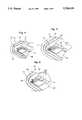
- FIG. 8is an exploded view of a resonant frequency identification tag in accordance with a preferred embodiment of the present invention.
- FIG. 9is a sectional side view of a portion of a housing of the resonant frequency identification tag of FIG. 8.
- the present inventionis directed to the fabrication of a thin, flexible resonant circuit with a custom integrated circuit (IC) and provides a method of wire-bonding the IC to the flexible substrate of the resonant circuit.
- ICintegrated circuit
- RFIDradio frequency identification
- U.S. Pat. No. 5,430,441discloses a transponding tag which transmits a digitally encoded signal in response to an interrogation signal.
- the tagcomprises a rigid substrate constructed from a plurality of dielectric layers and conductive layers and includes an integrated circuit embedded entirely within a hole in the substrate and tab bonded to conductive foil traces.
- Another RFID tagis disclosed in U.S. Pat. No. 5,444,223 to Blama.
- Blamarecognized the advantage of constructing a tag from low cost, flexible materials, such as paper. However, rather than store a predetermined identification code in a single integrated circuit, Blama constructed a tag using a plurality of circuits, each circuit representing a single bit of information.
- thin, flexible RFID tagsare made utilizing a very thin substrate of a dielectric material, such as polyethylene, laminated on both sides with a very thin layer of conductive material, such as aluminum foil, which is thereafter photo-printed and etched to form a two-sided circuit consisting of at least one inductor connected with one or more capacitors thereby forming a resonant circuit.
- a dielectric materialsuch as polyethylene
- conductive materialsuch as aluminum foil
- FIG. 1a schematic diagram of an equivalent electrical circuit of a resonant frequency identification tag 10 in accordance with a preferred embodiment of the present invention.
- the tag 10comprises a resonant circuit 12 electrically connected to an integrated circuit (IC)
- the resonant circuit 12may comprise one or more inductive elements electrically connected to one or more capacitive elements.
- the resonant circuit 12is formed by the combination of a single inductive element, inductor, or coil L electrically connected with a capacitive element or capacitance C ANT in a series loop.
- the frequency of the resonant circuit 12depends upon the values of the inductor coil L and the capacitor C ANT .
- Such a resonant circuitis shown and described in detail in U.S. Pat. No. 5,276,431, which is hereby incorporated by reference.
- the size of the inductor L and the value of the capacitor C ANTare determined based upon the desired resonant frequency of the resonant circuit 12 and the need to maintain a low induced voltage across the plates of the capacitor.
- tags 10are constructed which operate at 13.56 MHz. Although the tag 10 includes a single inductive element L and a single capacitor element C ANT , multiple inductor and capacitor elements could alteratively be employed.
- the IC 14stores a predetermined digital value, which can be used for a variety of purposes, such as to identify a particular object or person associated with the tag 10.
- the stored digital valuemay be unique to each tag 10, or in some instances, it may be desirable for two or more tags to have the same stored digital value.
- the IC 14could be used to store product warranty information.
- a proximity reader or interrogator device(not shown) is used to read the information stored in the IC 14. In operation, the proximity reader creates an electromagnetic field at the resonant frequency of the resonant circuit 12. When the tag 10 is placed proximate to the reader and in the electromagnetic field, a voltage is induced on the inductive coil L, which provides power to the IC 14 at the ANT input of the IC 14.
- the IC 14internally rectifies the induced AC voltage at the ANT input to provide an internal DC voltage source. When the internal DC voltage reaches a level that assures proper operation of the IC 14, the IC 14 functions to output the digital value stored therein at the MOD output of the IC 14.
- a modulation capacitor C MODis connected to the MOD output of the IC 14 and to the resonant circuit 12.
- the IC output pulsesswitch the capacitor C MOD into and out of the resonant circuit 12 by making and breaking ground connections to change the overall capacitance of the resonant circuit 12 in accordance with the stored data, which changes the resonant frequency of the resonant circuit 12, detuning it from the principal operational frequency to a predetermined higher frequency.
- the readerdetects the consumption of energy within its electromagnetic field. Data pulses of the tag 10 are created by the tuning and detuning of the resonant circuit 12. The reader senses the changes in the consumption of energy to determine the digital data value output from the IC 14.
- the IC 14also includes a power return or GND output and one or more additional inputs 16 which are used for programming the IC 14 (i.e. storing or altering the digital value therein).
- the IC 14comprises 64 bits of nonvolatile memory and the reader and tag 10 operate at 13.56 MHz.
- memory chips having a either a greater or smaller storage capacitymay be used such that the IC 14 stores more or fewer memory bits.
- the resonant circuit 12 and the readermay operate at radio frequencies other than 13.56 MHz.
- the tag 20like the tag 10, includes a resonant circuit comprising an inductor in the form of a coil 22 and a capacitor 24.
- the capacitor 24comprises two plates located on opposite sides or principal surfaces of a substrate 26.
- the inductor coil 22is located on one of the principal surfaces of the substrate 26 and comprises a coil which extends proximate to and around a peripheral outer edge 28 of the substrate 26. Since only one side of the tag 20 is shown, only one plate of the capacitor 24 is shown in FIG. 2.
- the plate of capacitor 24includes a plurality of fingers or extensions 30 which are provided for tuning the resonant circuit. That is, the fingers 30 may be cut, etched or otherwise trimmed and removed to change the value of the capacitor 24, and thus the resonant frequency of the resonant circuit 12.
- the substrate 26comprises a generally rectangular, planar insulative or dielectric material which is preferably flexible, such as paper or a polymeric material.
- the substrate 26comprises polyethylene.
- the substrate 26may be constructed of other materials, such as any solid material or composite structures of materials as long as the substrate 26 is insulative and can be used as a dielectric.
- the circuit elements and components of the resonant circuit 12are formed on both principal surfaces of the substrate 26 by patterning conductive material on the surfaces of the substrate 26.
- a first conductive patternis imposed on the first side or surface of the substrate 26, which surface is arbitrarily selected as the top surface of the tag 20, and a second conductive pattern is imposed on the opposite or second side or surface (not shown) of the substrate 26, sometimes referred to as the back or bottom surface.
- the conductive patternsmay be formed on the substrate surfaces with electrically conductive materials of a known type and in a manner which is well known in the electronic article surveillance art.
- the conductive materialis preferably patterned by a subtractive process (i.e. etching), whereby unwanted material is removed by chemical attack after desired material has been protected, typically with a printed on etch resistant ink.
- the conductive materialcomprises an aluminum foil.
- conductive materialse.g., conductive foils or inks, gold, nickel, copper, phosphor bronzes, brasses, solders, high density graphite or silver-filled conductive epoxies
- conductive foils or inksgold, nickel, copper, phosphor bronzes, brasses, solders, high density graphite or silver-filled conductive epoxies
- the first and second conductive patternsestablish at least one resonant circuit, such as the resonant circuit 12, having a resonant frequency within a predetermined operational frequency range, such as the aforementioned preferred frequency of 13.56 MHz.
- the resonant circuit 12is formed by the combination of a single inductive element, inductor, or coil L electrically connected with a single capacitive element or capacitance C ANT in a series loop.
- the inductive element L formed by the coil portion 22 of the first conductive patternis formed as a spiral coil of conductive material on a first principal surface of the substrate 26 and the capacitive element C ANT , as previously discussed, is comprised of a first plate formed by a generally rectangular plate (shown at 24) of the first conductive pattern and a second plate formed by a corresponding, aligned generally rectangular plate of the second conductive pattern (not shown).
- the first and second platesare generally in registry and are separated by the dielectric substrate 26.
- the first plate of the capacitor element C ANTis electrically connected to one end of the inductor coil 22.
- the second plate of the capacitor element C ANTis electrically connected by a weld connection (not shown) extending through the substrate 26 to connect the second plate to the other end of the inductor coil 22, thereby connecting the inductive element L to the capacitor element C ANT in a well known manner.
- the substrate 26 and the first and second conductive patternsis approximately 3.3 mils thick, with the substrate 26 being about 1.0 mil thick, the first conductive pattern (i.e. the coil layer or side shown in FIGS. 2 and 3) being about 2.0 mils thick and the second conductive pattern being about 0.3 mils thick. Since the substrate 26 is relatively thin and very flexible, it has been found that the substrate 26 does not, by itself, provide adequate support for receiving the IC 14 and maintaining the IC 14 in a firm or stable position such that electrical connections between the IC 14 and the resonant circuit 12 may be made which are strong and not readily broken or compromised. Accordingly, the present invention provides an IC receiving or attachment area 32 for receiving and supporting the IC 14.
- the IC attachment area 32is located on a surface of the substrate 26 and is constructed of a material suitable to sufficiently support the IC 14.
- the IC attachment area 32provides a stable surface to which the IC 14 may be attached or secured so that the IC 14 does not move relative to the substrate 26 and the resonant circuit 12 during an ultrasonic wirebonding operation.
- the IC attachment area 32has the same general dimensions as the IC 14 (e.g. generally rectangular in shape) but is of somewhat greater dimensions than the IC 14 so that it is not overly difficult to place the IC 14 on the IC attachment area 32.
- the IC attachment area 14is constructed of the same material as the first conductive pattern and is formed on the substrate 26 at the same time that the resonant circuit 12 is formed on the substrate 26.
- the IC attachment area 32should be located as close as possible to those areas or pads to which the IC 14 is to be electrically connected so that the electrical connections are not excessive in length.
- the IC attachment area 32is located at an upper right-hand side of the top surface of the substrate 26 proximate to, but not in contact with the coil 22 or the capacitor 24 such that the attachment area 32 is physically and electrically isolated from the other components. This location is suitable because it allows the IC 14 to be positioned or located proximate to each of the areas or pads to which it will be electrically connected.
- the tag 34comprises a substrate 26, an inductive coil 22 which functions as an antenna, and a capacitor 24 having fingers or extensions 30 to permit adjusting the value of the capacitor 24.
- the substrate 26comprises polyethylene which is formed in sheets and the inductive coil 22 and the capacitor 24 comprise etched aluminum foil, as previously described.
- the tag 34also includes an IC attachment area 36 which comprises a filled in corner or shoulder of the inductive coil 22. In contrast to the isolated or floating IC attachment area 32 (FIG.
- the IC attachment area 36as an integral portion of the conductive pattern on one side of the substrate 26 surface provides a more stable support surface for the IC 14 because movement of the substrate 26 is absorbed over a greater area (e.g., vibration of the IC attachment area 36 caused by ultrasonic energy during wire bonding is absorbed not only by the IC attachment area 36, but also by the coil 22). Providing a more stable or stiff support area for the IC 14 is important in being able to properly wire bond the IC 14 to the resonant circuit 12, as described hereinafter.
- a plurality of bonding padsare also formed on the first side of the substrate 26 to which the IC 14 is electrically connected.
- a first bonding pad 38is provided for connecting to the ANT input of the IC 14.
- a second bonding pad 40is provided for connecting to the MOD output of the IC 14, and a plurality of bonding pads 42 are provided for connecting to the additional inputs 16 of the IC 14 used for programming the IC 14, as previously described.
- Each of the bonding pads 38, 40, 42are formed of a conductive material and preferably are constructed of the same material as the first conductive pattern and are formed on the substrate 26 at the same time that the resonant circuit is formed on the substrate 26.
- the GND output of the IC 14is connected to the coil 22 at a location on the coil 22 proximate to the IC
- the IC 14is wire bonded to the bonding pads 38, 40, 42 and to the coil 22 with wires 44 (FIG. 6) using an ultra sonic welding process.
- a wire bonder with a vacuum plenum tableis used to interconnect an input/output pad on the IC 14 to a corresponding bonding pad 38/40/42 on the substrate 26 using a conductive wire, such as a 0.00125 inch aluminum wire.
- FIG. 7is a flow chart of the wire bonding process 50.
- proper cleaning of the bonding pads 38, 40 42, adhesively affixing the IC 14 to the IC attachment area 32/36, and securely holding the substrate 26 in a fixed position during the welding or wire bonding processare each important steps in ensuring a proper wire bond connection is made between the IC 14 and the bonding pads 38, 40, 42.
- the resonant circuit 12is die cut from a web formed as part of the manufacturing process having a plurality of individual resonant circuits 12 formed thereon.
- an area of the substrate 26 and the resonant circuit 12 proximate to and including the IC attachment area 36referred to generally as the IC bond attach area 46 (FIG. 4) is chemically cleaned at step 54 to remove any photoresist material which remains on the IC bond attach area 46 after the formation of the resonant circuit 12.
- the IC bond attach area 46is cleaned with acetone using a cotton swab.
- the resonant circuit 12is placed in a plenum or workholder designed to receive and securely hold the resonant circuit 12.
- the plenumincludes a recess which is sized and shaped to receive the resonant circuit 12.
- plenumsare known and commercially available which hold a workpiece within the plenum by vacuum pressure, it has been found that merely using vacuum pressure to hold the resonant circuit 12 within the plenum is not sufficient for maintaining the flexible substrate 26 therein and performing a wirebonding operation thereon. Accordingly, in the preferred manufacturing process, the resonant circuit 12 is held within the recess of the plenum both by vacuum pressure and by placing an adhesive means in the plenum circuit receiving area.
- the adhesive means for attaching the resonant circuit 12 to the plenumis strong enough to hold the resonant circuit 12 is place on the plenum, yet allows the resonant circuit 12 to also be removed from the plenum without tearing or damaging the resonant circuit 12.
- an adhesivepreferably an epoxy
- the IC 14is attached to the IC attachment area 32/36 with such an adhesive in order to maintain the IC 14 in position and to ensure that the IC 14 does not move during the wire bonding operation.
- the IC 14is attached to the IC attachment area 32/36 with an ultraviolet (UV) curable adhesive, such as a UV curable epoxy.
- UVultraviolet
- step 60the IC 14 is placed in the center of the IC attachment area 32/26.
- a vacuum-assist pickup toolmay be used to pick up and place the IC 14 on the IC attachment area 32/26. Care is taken to assure that the IC 14 is properly oriented and seated squarely and that there is a sufficient fillet of epoxy around the IC 14. Coated tweezers or wooden paddles may be used to aid in the alignment of the IC 14. Care also is taken to avoid scratching or getting epoxy on a top side of the IC 14 or the bonding pads 38, 40, 42.
- the epoxyis cured by placing the resonant circuit 12 through a UV cure conveyor oven.
- the UV cure conveyor ovenuses ultraviolet light to cure the epoxy at a temperature of approximately 60° C. It is preferred to cure the epoxy at 60° C., since higher temperatures could destroy or damage the substrate 26 and the flexible circuit 12.
- step 64those areas of the bonding pads 38, 40, 42 to which the wires 44 will be bonded, denoted as wire bond area 48 (FIG. 5), are cleaned to remove oxidation (e.g., AlO 2 ) and also to provide texture to the wire bond area 48 of the conductive material. Adding texture to the wire bond area 48 acts as an energy director and provides extra conductive material which is conducive to welding the wires 44 to the bonding pads 38, 40, 42. Accordingly, the cleaning step 64 is done with a mild abrasive, such as a synthetic steel wool scrubbing pad or a pencil eraser. It is also preferred that the cleaning step 64 be performed just prior to the wire bonding step in order to ensure that there is minimal or no oxidation on the conductive material during the wire bonding step.
- oxidatione.g., AlO 2
- Adding texture to the wire bond area 48acts as an energy director and provides extra conductive material which is conducive to welding the wires 44 to the bonding pads 38, 40, 42.
- the wires 44are bonded to the IC 14 and the bonding pads 38, 40, 42 (FIG. 6).
- the wire 44is a 0.00125 inch aluminum wire having a break strength of 18-20 gm.
- the wire 44is bonded to the bonding pads 38, 40, 42 and the IC 14 using a bonding apparatus and an ultrasonic generator of a type which is presently commercially available.
- the bond strengthis greater than 6 gm and the wire loop height does not exceed 0.015 inches.
- the resonant circuit 12is constructed using a flexible substrate 26, it is important that the resonant circuit 12 be held firmly during the wire bonding process.
- the resonant circuit 12be both adhesively held in the plenum and held by vacuum pressure to ensure that the ultrasonic energy generated by the wire bonding apparatus and directed to the IC 14 and the bonding pads 38, 40, 42 is not lost by movement or vibration of the IC 14 and/or the substrate 26.
- the wire bonding apparatususes sonic vibration to partially melt portions of the wire 44 and bond the wire 44 to the bonding pads, 38, 40, 42, respectively.
- the combination of adhesively securing the resonant circuit 12 to the wire bonding machine, using vacuum pressure to secure the resonant circuit 12 to the wire bonding machine, and attaching the IC 14 to the resonant circuit 12 using epoxyadequately holds the resonant circuit 12 and the IC 14 such that effective wire bonds are formed.
- a protective covering or encapsulant 45(FIG. 9) is placed at least over the wire bonds in step 68.
- the encapsulant 45covers the entire IC 14, the wires 44 and the wire bonds.
- the encapsulant 45is applied using an encapsulant pneumatic dispenser, as is known to those of ordinary skill in the art.
- the encapsulant 45is a light curing resin and that the finished height of the encapsulant 45 over the wire bonded IC 14 does not exceed 0.025 inches and that the diameter of the encapsulant 45 does not exceed 0.25 inches in order for the encapsulated IC 14 to fit within a recess of a polymeric housing, as hereinafter described.
- the encapsulant 45is cured by placing the circuit 12 in a UV cure conveyor oven.
- the encapsulant 45is cured using ultraviolet light at a temperature of approximately 60° C.
- the encapsulant 45is not cured by baking because the preferred polyethylene substrate 26 melts at approximately 75°0 C. Accordingly, baking would damage or destroy the substrate 26.
- the frequency of the resonant circuit 12is measured by using a spectrum analyzer or a test setup using a frequency generator and a display monitor.
- the capacitor 24is trimmed by cutting and removing one or more of the capacitor fingers 30, if necessary, in order to ensure that the resonant circuit 12 operates at a predetermined resonant frequency, which in the preferred embodiment is between 13.6 MHz to 13.8 MHz.
- the IC 14is programmed to store the desired data in the IC 14 in a manner well known in the art, preferably, by attaching probe leads from a computer to the programming pads 42.
- the proximity card 90comprises the RFID tag 10, a housing 92, a double-sided transfer adhesive tape 94, and a cover label or backing 96.
- the housing 92includes a recess 98 located and sized for receiving the encapsulated IC 14 of the tag 10.
- the transfer adhesive tape 94also includes a cutout area 100 in a corner thereof corresponding to the recess 98 and the IC 14 so that the IC 14 can be received within the recess 98.
- step 76the double-sided transfer adhesive tape 94 is applied to the undersurface of the housing 92 in an orientation such that the cutout area 100 corresponds with the recess 98.
- step 78the tag 10 is attached to the transfer adhesive tape 94 on the housing 92 and the IC 14 is received within the recess 98 of the housing 92.
- step 80the cover label 96 is applied to the tag 10 with an adhesive (not shown).
- the cover label 96may include printed indicia on its outer surface for advertising or identification purposes.
- the proximity card 90is preferably formed in a rectangular shape to resemble a credit card in both size and shape, which is convenient for human handling.
- a sequence number and a date code for the card 90may be stamped on an outer surface of the housing 92 or on the cover label 96.
- the housing 92is preferably constructed of a polymeric material, such as polyvinylchloride and formed by injection molding or in some other manner, as is known in the art.
- the transfer adhesive tape 94is preferably a double-sided, double-lined two mil adhesive tape, which is generally commercially available in packaged rolls.
- the proximity card 90may be used as an access control card as is known by those of skill in the art.
- the tag 10could be used as a security label which is placed on a retail item for use in security or product warranty purposes. It will also be apparent to those of skill in the art that the tag 10 can be used in other commercial applications.
- the present embodimentcomprises a method of wire bonding an IC to a flexible substrate composed of a material which cannot withstand high temperatures required for soldering processes.
Landscapes
- Engineering & Computer Science (AREA)
- Microelectronics & Electronic Packaging (AREA)
- Computer Hardware Design (AREA)
- Physics & Mathematics (AREA)
- General Physics & Mathematics (AREA)
- Power Engineering (AREA)
- Theoretical Computer Science (AREA)
- Condensed Matter Physics & Semiconductors (AREA)
- Computer Networks & Wireless Communication (AREA)
- Credit Cards Or The Like (AREA)
- Wire Bonding (AREA)
- Burglar Alarm Systems (AREA)
Abstract
Description
Claims (21)
Priority Applications (16)
| Application Number | Priority Date | Filing Date | Title |
|---|---|---|---|
| US08/681,195US5708419A (en) | 1996-07-22 | 1996-07-22 | Method of wire bonding an integrated circuit to an ultraflexible substrate |
| AU24915/97AAU715326B2 (en) | 1996-07-22 | 1997-06-16 | Method of wire bonding an integrated circuit to an ultraflexible substrate |
| IL12108797AIL121087A (en) | 1996-07-22 | 1997-06-16 | Method of wire bonding an integrated circuit to an ultraflexible substrate |
| NZ328217ANZ328217A (en) | 1996-07-22 | 1997-07-01 | Attaching an integrated circuit to at least one electrical conductor on a flexible substrate and rfid tag comprising the substrate |
| CN97111895ACN1108634C (en) | 1996-07-22 | 1997-07-03 | Method of wire bonding integrated circuit to ultraflexible substrate |
| TW086109739ATW342582B (en) | 1996-07-22 | 1997-07-10 | Method of wire bonding an integrated circuit to an ultraflexible substrate |
| ARP970103099AR007853A1 (en) | 1996-07-22 | 1997-07-11 | ELECTRICAL CONNECTION METHOD, FROM AN INTEGRATED CIRCUIT TO AT LEAST AN ELECTRICAL CONDUCTOR IN A FLEXIBLE SUBSTRATE AND A RADIO FREQUENCY IDENTIFICATION LABEL |
| CA 2210833CA2210833C (en) | 1996-07-22 | 1997-07-18 | Method of wire bonding an integrated circuit to an ultraflexible substrate |
| DE1997638172DE69738172T2 (en) | 1996-07-22 | 1997-07-21 | An integrated circuit on an ultrafine substrate and a method for wire bonding between an integrated circuit and an ultra-fast substrate |
| MX9705524AMX9705524A (en) | 1996-07-22 | 1997-07-21 | Method of wire bonding an integrated circuit to an ultraflexible substrate. |
| ES97112463TES2294790T3 (en) | 1996-07-22 | 1997-07-21 | INTEGRATED CIRCUIT OF AN ULTRAFLEXIBLE SUBSTRATE AND A THREAD UNION PROCEDURE OF A CIRCUIT INTEGRATED TO AN ULTRAFLEXIBLE SUBSTRATE. |
| AT97112463TATE375004T1 (en) | 1996-07-22 | 1997-07-21 | AN INTEGRATED CIRCUIT ON AN ULTRA-FLEXIBLE SUBSTRATE AND A METHOD FOR A WIRE CONNECTION BETWEEN AN INTEGRATED CIRCUIT AND AN ULTRA-FLEXIBLE SUBSTRATE |
| EP19970112463EP0821406B1 (en) | 1996-07-22 | 1997-07-21 | An integrated circuit on an ultra-flexible substrate and a method of wire bonding an integrated circuit to an ultra-flexible substrate |
| KR1019970035517AKR100543349B1 (en) | 1996-07-22 | 1997-07-22 | How to Wire Bond Integrated Circuits on Super Flexible Boards |
| JP19540397AJP4290233B2 (en) | 1996-07-22 | 1997-07-22 | Method of wire bonding an integrated circuit to a super flexible substrate |
| JP2008059376AJP4342589B2 (en) | 1996-07-22 | 2008-03-10 | RFID security tag |
Applications Claiming Priority (1)
| Application Number | Priority Date | Filing Date | Title |
|---|---|---|---|
| US08/681,195US5708419A (en) | 1996-07-22 | 1996-07-22 | Method of wire bonding an integrated circuit to an ultraflexible substrate |
Publications (1)
| Publication Number | Publication Date |
|---|---|
| US5708419Atrue US5708419A (en) | 1998-01-13 |
Family
ID=24734222
Family Applications (1)
| Application Number | Title | Priority Date | Filing Date |
|---|---|---|---|
| US08/681,195Expired - LifetimeUS5708419A (en) | 1996-07-22 | 1996-07-22 | Method of wire bonding an integrated circuit to an ultraflexible substrate |
Country Status (15)
| Country | Link |
|---|---|
| US (1) | US5708419A (en) |
| EP (1) | EP0821406B1 (en) |
| JP (2) | JP4290233B2 (en) |
| KR (1) | KR100543349B1 (en) |
| CN (1) | CN1108634C (en) |
| AR (1) | AR007853A1 (en) |
| AT (1) | ATE375004T1 (en) |
| AU (1) | AU715326B2 (en) |
| CA (1) | CA2210833C (en) |
| DE (1) | DE69738172T2 (en) |
| ES (1) | ES2294790T3 (en) |
| IL (1) | IL121087A (en) |
| MX (1) | MX9705524A (en) |
| NZ (1) | NZ328217A (en) |
| TW (1) | TW342582B (en) |
Cited By (90)
| Publication number | Priority date | Publication date | Assignee | Title |
|---|---|---|---|---|
| US5861809A (en)* | 1997-09-22 | 1999-01-19 | Checkpoint Systems, Inc. | Deactivateable resonant circuit |
| US5982284A (en)* | 1997-09-19 | 1999-11-09 | Avery Dennison Corporation | Tag or label with laminated thin, flat, flexible device |
| US6031242A (en)* | 1998-01-23 | 2000-02-29 | Zevatech, Inc. | Semiconductor die in-flight registration and orientation method and apparatus |
| US6077022A (en)* | 1997-02-18 | 2000-06-20 | Zevatech Trading Ag | Placement machine and a method to control a placement machine |
| US6091607A (en)* | 1998-12-10 | 2000-07-18 | Checkpoint Systems, Inc. | Resonant tag with a conductive composition closing an electrical circuit |
| US6114962A (en)* | 1998-10-15 | 2000-09-05 | Intermec Ip Corp. | RF tag having strain relieved stiff substrate and hydrostatic protection for a chip mounted thereto |
| US6129040A (en)* | 1997-09-05 | 2000-10-10 | Esec Sa | Semi-conductor mounting apparatus for applying adhesive to a substrate |
| US6133835A (en)* | 1997-12-05 | 2000-10-17 | U.S. Philips Corporation | Identification transponder |
| US6135339A (en)* | 1998-01-26 | 2000-10-24 | Esec Sa | Ultrasonic transducer with a flange for mounting on an ultrasonic welding device, in particular on a wire bonder |
| US6147662A (en)* | 1999-09-10 | 2000-11-14 | Moore North America, Inc. | Radio frequency identification tags and labels |
| US6157870A (en)* | 1997-02-18 | 2000-12-05 | Zevatech Trading Ag | Apparatus supplying components to a placement machine with splice sensor |
| US6163260A (en)* | 1998-12-10 | 2000-12-19 | Intermec Ip Corp. | Linerless label tracking system |
| US6164551A (en)* | 1997-10-29 | 2000-12-26 | Meto International Gmbh | Radio frequency identification transponder having non-encapsulated IC chip |
| US6179938B1 (en) | 1997-10-30 | 2001-01-30 | Esec Sa | Method and apparatus for aligning the bonding head of a bonder, in particular a die bonder |
| US6181287B1 (en)* | 1997-03-10 | 2001-01-30 | Precision Dynamics Corporation | Reactively coupled elements in circuits on flexible substrates |
| US6185815B1 (en) | 1997-12-07 | 2001-02-13 | Esec Sa | Semiconductor mounting apparatus with a chip gripper travelling back and forth |
| US6204764B1 (en)* | 1998-09-11 | 2001-03-20 | Key-Trak, Inc. | Object tracking system with non-contact object detection and identification |
| US6226619B1 (en)* | 1998-10-29 | 2001-05-01 | International Business Machines Corporation | Method and system for preventing counterfeiting of high price wholesale and retail items |
| US6249227B1 (en)* | 1998-01-05 | 2001-06-19 | Intermec Ip Corp. | RFID integrated in electronic assets |
| US6262692B1 (en) | 1999-01-13 | 2001-07-17 | Brady Worldwide, Inc. | Laminate RFID label and method of manufacture |
| US6317044B1 (en) | 1996-09-05 | 2001-11-13 | Key-Track, Inc. | Inventoriable object control and tracking system |
| US6392543B2 (en) | 1998-09-11 | 2002-05-21 | Key-Trak, Inc. | Mobile object tracking system |
| US6427913B1 (en) | 1998-09-11 | 2002-08-06 | Key-Trak, Inc. | Object control and tracking system with zonal transition detection |
| WO2001082009A3 (en)* | 2000-04-20 | 2002-08-22 | Cogiscan Inc | Automated manufacturing control system |
| US6501379B2 (en) | 1998-09-11 | 2002-12-31 | Key-Trak, Inc. | Object carriers for an object control and tracking system |
| US6509217B1 (en) | 1999-10-22 | 2003-01-21 | Damoder Reddy | Inexpensive, reliable, planar RFID tag structure and method for making same |
| US20030075608A1 (en)* | 2000-03-21 | 2003-04-24 | Atherton Peter S | Tamper indicating radio frequency identification label |
| US20030169153A1 (en)* | 2000-03-28 | 2003-09-11 | Philipp Muller | Rfid-label with an element for regulating the resonance frequency |
| US20030184437A1 (en)* | 1998-09-11 | 2003-10-02 | Maloney William C. | Object carriers and lighted tags for an object control and tracking system |
| US6696952B2 (en) | 2000-08-04 | 2004-02-24 | Hei, Inc. | Structures and assembly methods for radio-frequency-identification modules |
| US6727817B2 (en) | 1998-09-11 | 2004-04-27 | Key-Trak, Inc. | Tamper detection and prevention for an object control and tracking system |
| US20040100382A1 (en)* | 2002-11-21 | 2004-05-27 | Hewlett-Packard Development Company, L.P. | Memory tag |
| US20040124983A1 (en)* | 1999-07-29 | 2004-07-01 | Sony Chemicals Corp. | IC card having a mica film for stable resonance frequency and enhanced antenna properties |
| US20040160337A1 (en)* | 2000-08-14 | 2004-08-19 | Computime, Ltd. | Alarm clock with remote control function |
| US20040183182A1 (en)* | 2002-01-23 | 2004-09-23 | Susan Swindlehurst | Apparatus incorporating small-feature-size and large-feature-size components and method for making same |
| US20040188531A1 (en)* | 2003-03-24 | 2004-09-30 | Gengel Glenn W. | RFID tags and processes for producing RFID tags |
| WO2004100366A2 (en) | 2003-05-01 | 2004-11-18 | Checkpoint Systems, Inc. | Lc resonant circuit with amplification device |
| US20040233591A1 (en)* | 2002-03-13 | 2004-11-25 | Devilbiss Alan D. | Rectifier utilizing a grounded antenna |
| US20050027604A1 (en)* | 1997-11-21 | 2005-02-03 | Matrics, Inc. | System and method for electronic inventory |
| US20050183817A1 (en)* | 2004-02-23 | 2005-08-25 | Eric Eckstein | Security tag system for fabricating a tag including an integrated surface processing system |
| US20050187837A1 (en)* | 2004-02-23 | 2005-08-25 | Eric Eckstein | Method and system for determining billing information in a tag fabrication process |
| US20050184873A1 (en)* | 2004-02-23 | 2005-08-25 | Eric Eckstein | Tag having patterned circuit elements and a process for making same |
| US20050184872A1 (en)* | 2004-02-23 | 2005-08-25 | Clare Thomas J. | Identification marking and method for applying the identification marking to an item |
| US20050183264A1 (en)* | 2004-02-23 | 2005-08-25 | Eric Eckstein | Method for aligning capacitor plates in a security tag and a capacitor formed thereby |
| US20050242964A1 (en)* | 1992-08-12 | 2005-11-03 | Tuttle John R | Miniature radio frequency transceiver |
| US20050270752A1 (en)* | 2001-05-31 | 2005-12-08 | Credelle Thomas L | Electronic devices with small functional elements supported on a carrier |
| US6980085B1 (en) | 1997-08-18 | 2005-12-27 | Micron Technology, Inc. | Wireless communication devices and methods of forming and operating the same |
| US20050284917A1 (en)* | 2004-06-24 | 2005-12-29 | Checkpoint Systems, Inc. | Die attach area cut-on-fly method and apparatus |
| US20060055531A1 (en)* | 2004-09-14 | 2006-03-16 | Honeywell International, Inc. | Combined RF tag and SAW sensor |
| US20060092013A1 (en)* | 2004-10-07 | 2006-05-04 | West Pharmaceutical Services, Inc. | Closure for a container |
| US20060103027A1 (en)* | 2004-11-18 | 2006-05-18 | Seiko Epson Corporation | Electronic component and method for manufacturing the same |
| US20060109129A1 (en)* | 2004-11-22 | 2006-05-25 | Curt Carrender | Transponder incorporated into an electronic device |
| US20060109130A1 (en)* | 2004-11-22 | 2006-05-25 | Hattick John B | Radio frequency identification (RFID) tag for an item having a conductive layer included or attached |
| US20060134836A1 (en)* | 2003-04-29 | 2006-06-22 | Knapp James H | Method of marking a low profile packaged semiconductor device |
| US7106201B2 (en)* | 1997-08-20 | 2006-09-12 | Micron Technology, Inc. | Communication devices, remote intelligent communication devices, electronic communication devices, methods of forming remote intelligent communication devices and methods of forming a radio frequency identification device |
| US20060248767A1 (en)* | 2005-04-28 | 2006-11-09 | Zih Corp. | Antimicrobial coating for identification devices |
| US20060254474A1 (en)* | 2005-05-11 | 2006-11-16 | Roth Arthur J | Shipping pallet equipped with a non-structural member carrying a readable device |
| US20070013487A1 (en)* | 2005-07-18 | 2007-01-18 | Jan Scholtz | Digital certificate on connectors and other products using RFID tags and/or labels as well as RFID reader/interrogator |
| US7168623B1 (en)* | 1998-10-23 | 2007-01-30 | Stmicroelectronics S.A. | Self-adhesive electronic circuit |
| US20070031992A1 (en)* | 2005-08-05 | 2007-02-08 | Schatz Kenneth D | Apparatuses and methods facilitating functional block deposition |
| US7190083B1 (en) | 2002-01-07 | 2007-03-13 | Vixs Systems, Inc. | High frequency integrated circuit using capacitive bonding |
| US20070097725A1 (en)* | 2005-10-27 | 2007-05-03 | Renesas Technology Corp. | Semiconductor integrated circuit and contactless electronic device using the same |
| US20070098942A1 (en)* | 2005-11-02 | 2007-05-03 | Checkpoint Systems, Inc. | In-mold chip attach |
| US20070102486A1 (en)* | 2005-10-24 | 2007-05-10 | Checkpoint Systems, Inc. | Wire embedded bridge |
| US20070114659A1 (en)* | 2005-11-18 | 2007-05-24 | Checkpoint Systems, Inc. | Rotary chip attach |
| US20070171129A1 (en)* | 2006-01-24 | 2007-07-26 | Avery Dennison Corporation | Radio frequency (RF) antenna containing element and methods of making the same |
| US7288432B2 (en) | 1999-03-16 | 2007-10-30 | Alien Technology Corporation | Electronic devices with small functional elements supported on a carrier |
| WO2007147593A1 (en) | 2006-06-21 | 2007-12-27 | Dynamic Systems Gmbh | Transponder comprising an electronic memory chip and magnetic circular antenna |
| US7353598B2 (en) | 2004-11-08 | 2008-04-08 | Alien Technology Corporation | Assembly comprising functional devices and method of making same |
| EP1950791A1 (en) | 2004-06-24 | 2008-07-30 | Checkpoint Systems, Inc. | Bonding machine for applying transponders and method |
| US7452748B1 (en) | 2004-11-08 | 2008-11-18 | Alien Technology Corporation | Strap assembly comprising functional block deposited therein and method of making same |
| US20090009412A1 (en)* | 2006-12-29 | 2009-01-08 | Warther Richard O | Printed Planar RFID Element Wristbands and Like Personal Identification Devices |
| US20090021377A1 (en)* | 2006-10-19 | 2009-01-22 | Upm Raflatac Oy | Tamperproof tag |
| US7542301B1 (en) | 2005-06-22 | 2009-06-02 | Alien Technology Corporation | Creating recessed regions in a substrate and assemblies having such recessed regions |
| US7551141B1 (en) | 2004-11-08 | 2009-06-23 | Alien Technology Corporation | RFID strap capacitively coupled and method of making same |
| US20090159202A1 (en)* | 2006-06-30 | 2009-06-25 | The Stanley Works | Method of manufacturing an adhesive mount for a leveling device |
| US20090225415A1 (en)* | 2005-12-23 | 2009-09-10 | Thomas Fergus Hughes | Laboratory slide |
| US7688206B2 (en) | 2004-11-22 | 2010-03-30 | Alien Technology Corporation | Radio frequency identification (RFID) tag for an item having a conductive layer included or attached |
| US7704346B2 (en) | 2004-02-23 | 2010-04-27 | Checkpoint Systems, Inc. | Method of fabricating a security tag in an integrated surface processing system |
| EP2192530A4 (en)* | 2007-09-14 | 2010-10-27 | Toppan Printing Co Ltd | ANTENNA SHEET, TRANSPONDER AND BOOK SHAPE |
| US7844505B1 (en) | 1997-11-21 | 2010-11-30 | Symbol Technologies, Inc. | Automated real-time distributed tag reader network |
| US20110024509A1 (en)* | 2009-07-29 | 2011-02-03 | Checkpoint Systems Inc. | Security labels with reinforced windows and methods of making the same |
| US20110226861A1 (en)* | 2005-04-06 | 2011-09-22 | Vanguard Identification Systems, Inc. | Printed Planar RFID Element Wristbands and Like Personal Identification Devices |
| US20110226857A1 (en)* | 1999-06-16 | 2011-09-22 | Vanguard Identification Systems, Inc. | Methods of making printed planar radio frequency identification elements |
| AU2008351057B2 (en)* | 2008-02-22 | 2012-04-26 | Toppan Printing Co., Ltd. | Transponder and book form |
| WO2013013184A3 (en)* | 2011-07-20 | 2013-05-02 | Visa International Service Association | Expansion device placement apparatus |
| US8931166B2 (en) | 2011-05-19 | 2015-01-13 | Tecnomar Oy | Manufacturing method of electrical bridges suitable for reel to reel mass manufacturing |
| US9231290B2 (en) | 2010-06-14 | 2016-01-05 | Avery Dennison Corporation | Method for making short run radio frequency identification tags and labels |
| US20190139881A1 (en)* | 2017-11-08 | 2019-05-09 | Idemia France | Security device such that a smart card |
| US10685273B2 (en) | 2016-10-07 | 2020-06-16 | Avery Dennison Retail Information Services, Llc | Vibratory feeder systems for RFID elements |
Families Citing this family (14)
| Publication number | Priority date | Publication date | Assignee | Title |
|---|---|---|---|---|
| US6630370B2 (en) | 1998-10-02 | 2003-10-07 | Shinko Electric Industries Co., Ltd. | Process for manufacturing IC card |
| DE19850353C1 (en)* | 1998-11-02 | 2000-03-16 | David Finn | Identification label for surface fixture or wrap-around fixture to object comprises multi-layer structure with identification layer for optical designation, reinforcement layer |
| US6522308B1 (en)* | 2000-01-03 | 2003-02-18 | Ask S.A. | Variable capacitance coupling antenna |
| GB2361584A (en)* | 2000-04-19 | 2001-10-24 | Motorola Israel Ltd | Multi-band antenna and switch system |
| KR100367301B1 (en)* | 2000-10-09 | 2003-01-09 | (주)이.씨테크날리지 | The making method and apparatus of card module |
| US6693541B2 (en)* | 2001-07-19 | 2004-02-17 | 3M Innovative Properties Co | RFID tag with bridge circuit assembly and methods of use |
| DE10232007A1 (en)* | 2002-07-15 | 2004-02-19 | Giesecke & Devrient Gmbh | Transponder for flat-shaped articles |
| JP2005129900A (en)* | 2003-09-30 | 2005-05-19 | Sanyo Electric Co Ltd | Circuit device and manufacturing method thereof |
| CN100369932C (en)* | 2005-04-07 | 2008-02-20 | 苏州大学 | Anti-human CD154 monoclonal antibody and its application |
| JP2007233703A (en)* | 2006-03-01 | 2007-09-13 | Minerva:Kk | Wireless tag and its manufacturing method |
| WO2010066955A1 (en) | 2008-12-11 | 2010-06-17 | Yves Eray | Rfid antenna circuit |
| WO2016018585A1 (en) | 2014-07-31 | 2016-02-04 | 3M Innovative Properties Company | Rfid tag on stretchable substrate |
| WO2016018777A2 (en)* | 2014-07-31 | 2016-02-04 | 3M Innovative Properties Company | Rfid tag on flexible substrate |
| CN109344949B (en)* | 2018-08-01 | 2020-06-16 | 浙江大学 | Anti-fake theftproof RFID label of antenna and circuit separation |
Citations (9)
| Publication number | Priority date | Publication date | Assignee | Title |
|---|---|---|---|---|
| US4381602A (en)* | 1980-12-29 | 1983-05-03 | Honeywell Information Systems Inc. | Method of mounting an I.C. chip on a substrate |
| US4656463A (en)* | 1983-04-21 | 1987-04-07 | Intelli-Tech Corporation | LIMIS systems, devices and methods |
| US5103210A (en)* | 1990-06-27 | 1992-04-07 | Checkpoint Systems, Inc. | Activatable/deactivatable security tag for use with an electronic security system |
| US5276431A (en)* | 1992-04-29 | 1994-01-04 | Checkpoint Systems, Inc. | Security tag for use with article having inherent capacitance |
| US5361491A (en)* | 1989-11-06 | 1994-11-08 | Nippon Mektron, Ltd. | Process for producing an IC-mounting flexible circuit board |
| US5430441A (en)* | 1993-10-12 | 1995-07-04 | Motorola, Inc. | Transponding tag and method |
| US5444223A (en)* | 1994-01-11 | 1995-08-22 | Blama; Michael J. | Radio frequency identification tag and method |
| US5528222A (en)* | 1994-09-09 | 1996-06-18 | International Business Machines Corporation | Radio frequency circuit and memory in thin flexible package |
| US5546654A (en)* | 1994-08-29 | 1996-08-20 | General Electric Company | Vacuum fixture and method for fabricating electronic assemblies |
Family Cites Families (10)
| Publication number | Priority date | Publication date | Assignee | Title |
|---|---|---|---|---|
| US4727246A (en)* | 1984-08-31 | 1988-02-23 | Casio Computer Co., Ltd. | IC card |
| JPS61157990A (en)* | 1984-12-29 | 1986-07-17 | Kyodo Printing Co Ltd | IC card |
| JPH0751390B2 (en)* | 1985-07-10 | 1995-06-05 | カシオ計算機株式会社 | IC card |
| US4857893A (en)* | 1986-07-18 | 1989-08-15 | Bi Inc. | Single chip transponder device |
| ES2040343T3 (en)* | 1987-06-08 | 1993-10-16 | Esselte Meto International Gmbh | MAGNETIC DEVICES. |
| US5304513A (en)* | 1987-07-16 | 1994-04-19 | Gao Gesellschaft Fur Automation Und Organisation Mbh | Method for manufacturing an encapsulated semiconductor package using an adhesive barrier frame |
| GB9222460D0 (en)* | 1992-10-26 | 1992-12-09 | Hughes Microelectronics Europa | Radio frequency baggage tag |
| NL9202067A (en)* | 1992-11-27 | 1994-06-16 | Dutch A & A Trading Bv | Detection label. |
| US5519201A (en)* | 1994-04-29 | 1996-05-21 | Us3, Inc. | Electrical interconnection for structure including electronic and/or electromagnetic devices |
| EP0704928A3 (en)* | 1994-09-30 | 1998-08-05 | HID Corporation | RF transponder system with parallel resonant interrogation and series resonant response |
- 1996
- 1996-07-22USUS08/681,195patent/US5708419A/ennot_activeExpired - Lifetime
- 1997
- 1997-06-16ILIL12108797Apatent/IL121087A/ennot_activeIP Right Cessation
- 1997-06-16AUAU24915/97Apatent/AU715326B2/ennot_activeCeased
- 1997-07-01NZNZ328217Apatent/NZ328217A/enunknown
- 1997-07-03CNCN97111895Apatent/CN1108634C/ennot_activeExpired - Lifetime
- 1997-07-10TWTW086109739Apatent/TW342582B/ennot_activeIP Right Cessation
- 1997-07-11ARARP970103099patent/AR007853A1/ennot_activeApplication Discontinuation
- 1997-07-18CACA 2210833patent/CA2210833C/ennot_activeExpired - Fee Related
- 1997-07-21ATAT97112463Tpatent/ATE375004T1/ennot_activeIP Right Cessation
- 1997-07-21MXMX9705524Apatent/MX9705524A/enunknown
- 1997-07-21DEDE1997638172patent/DE69738172T2/ennot_activeExpired - Lifetime
- 1997-07-21ESES97112463Tpatent/ES2294790T3/ennot_activeExpired - Lifetime
- 1997-07-21EPEP19970112463patent/EP0821406B1/ennot_activeExpired - Lifetime
- 1997-07-22JPJP19540397Apatent/JP4290233B2/ennot_activeExpired - Fee Related
- 1997-07-22KRKR1019970035517Apatent/KR100543349B1/ennot_activeExpired - Fee Related
- 2008
- 2008-03-10JPJP2008059376Apatent/JP4342589B2/ennot_activeExpired - Fee Related
Patent Citations (9)
| Publication number | Priority date | Publication date | Assignee | Title |
|---|---|---|---|---|
| US4381602A (en)* | 1980-12-29 | 1983-05-03 | Honeywell Information Systems Inc. | Method of mounting an I.C. chip on a substrate |
| US4656463A (en)* | 1983-04-21 | 1987-04-07 | Intelli-Tech Corporation | LIMIS systems, devices and methods |
| US5361491A (en)* | 1989-11-06 | 1994-11-08 | Nippon Mektron, Ltd. | Process for producing an IC-mounting flexible circuit board |
| US5103210A (en)* | 1990-06-27 | 1992-04-07 | Checkpoint Systems, Inc. | Activatable/deactivatable security tag for use with an electronic security system |
| US5276431A (en)* | 1992-04-29 | 1994-01-04 | Checkpoint Systems, Inc. | Security tag for use with article having inherent capacitance |
| US5430441A (en)* | 1993-10-12 | 1995-07-04 | Motorola, Inc. | Transponding tag and method |
| US5444223A (en)* | 1994-01-11 | 1995-08-22 | Blama; Michael J. | Radio frequency identification tag and method |
| US5546654A (en)* | 1994-08-29 | 1996-08-20 | General Electric Company | Vacuum fixture and method for fabricating electronic assemblies |
| US5528222A (en)* | 1994-09-09 | 1996-06-18 | International Business Machines Corporation | Radio frequency circuit and memory in thin flexible package |
Non-Patent Citations (2)
| Title |
|---|
| John Bowers, "Road to Intelligent Taging is Paved With Opportunities", Automatic I.D. News, (Oct., 1995), pp. 86-87. |
| John Bowers, Road to Intelligent Taging is Paved With Opportunities , Automatic I.D. News, (Oct., 1995), pp. 86 87.* |
Cited By (215)
| Publication number | Priority date | Publication date | Assignee | Title |
|---|---|---|---|---|
| US20050242964A1 (en)* | 1992-08-12 | 2005-11-03 | Tuttle John R | Miniature radio frequency transceiver |
| US7746230B2 (en) | 1992-08-12 | 2010-06-29 | Round Rock Research, Llc | Radio frequency identification device and method |
| US7649463B2 (en)* | 1992-08-12 | 2010-01-19 | Keystone Technology Solutions, Llc | Radio frequency identification device and method |
| US7583192B2 (en) | 1992-08-12 | 2009-09-01 | Keystone Technology Solutions, Llc | Radio frequency identification device and method |
| US8018340B2 (en) | 1992-08-12 | 2011-09-13 | Round Rock Research, Llc | System and method to track articles at a point of origin and at a point of destination using RFID |
| US20080129510A1 (en)* | 1992-08-12 | 2008-06-05 | Tuttle John R | Radio Frequency Identification Device And Method |
| US20070103316A1 (en)* | 1992-08-12 | 2007-05-10 | Tuttle John R | Radio frequency identification device and method |
| US6707380B2 (en) | 1995-09-08 | 2004-03-16 | Key-Trak, Inc. | Inventoriable-object control and tracking system |
| US7342494B2 (en) | 1995-09-08 | 2008-03-11 | Key Control Holding, Inc. | Inventoriable-object control and tracking system |
| US6317044B1 (en) | 1996-09-05 | 2001-11-13 | Key-Track, Inc. | Inventoriable object control and tracking system |
| US6077022A (en)* | 1997-02-18 | 2000-06-20 | Zevatech Trading Ag | Placement machine and a method to control a placement machine |
| US6157870A (en)* | 1997-02-18 | 2000-12-05 | Zevatech Trading Ag | Apparatus supplying components to a placement machine with splice sensor |
| US6181287B1 (en)* | 1997-03-10 | 2001-01-30 | Precision Dynamics Corporation | Reactively coupled elements in circuits on flexible substrates |
| US20060097849A1 (en)* | 1997-08-18 | 2006-05-11 | Dando Ross S | Wireless communication devices and methods of forming and operating the same |
| US6980085B1 (en) | 1997-08-18 | 2005-12-27 | Micron Technology, Inc. | Wireless communication devices and methods of forming and operating the same |
| US20070007345A1 (en)* | 1997-08-20 | 2007-01-11 | Tuttle Mark E | Electronic communication devices, methods of forming electrical communication devices, and communications methods |
| US7948382B2 (en) | 1997-08-20 | 2011-05-24 | Round Rock Research, Llc | Electronic communication devices, methods of forming electrical communication devices, and communications methods |
| US7106201B2 (en)* | 1997-08-20 | 2006-09-12 | Micron Technology, Inc. | Communication devices, remote intelligent communication devices, electronic communication devices, methods of forming remote intelligent communication devices and methods of forming a radio frequency identification device |
| US7839285B2 (en) | 1997-08-20 | 2010-11-23 | Round Rock Resarch, LLC | Electronic communication devices, methods of forming electrical communication devices, and communications methods |
| US6129040A (en)* | 1997-09-05 | 2000-10-10 | Esec Sa | Semi-conductor mounting apparatus for applying adhesive to a substrate |
| US5982284A (en)* | 1997-09-19 | 1999-11-09 | Avery Dennison Corporation | Tag or label with laminated thin, flat, flexible device |
| AU738644B2 (en)* | 1997-09-22 | 2001-09-20 | Checkpoint Systems, Inc. | Deactivateable resonant circuit |
| US5861809A (en)* | 1997-09-22 | 1999-01-19 | Checkpoint Systems, Inc. | Deactivateable resonant circuit |
| WO1999016032A1 (en)* | 1997-09-22 | 1999-04-01 | Checkpoint Systems, Inc. | Deactivateable resonant circuit |
| US6164551A (en)* | 1997-10-29 | 2000-12-26 | Meto International Gmbh | Radio frequency identification transponder having non-encapsulated IC chip |
| US6179938B1 (en) | 1997-10-30 | 2001-01-30 | Esec Sa | Method and apparatus for aligning the bonding head of a bonder, in particular a die bonder |
| US7844505B1 (en) | 1997-11-21 | 2010-11-30 | Symbol Technologies, Inc. | Automated real-time distributed tag reader network |
| US20050027604A1 (en)* | 1997-11-21 | 2005-02-03 | Matrics, Inc. | System and method for electronic inventory |
| US6133835A (en)* | 1997-12-05 | 2000-10-17 | U.S. Philips Corporation | Identification transponder |
| US6185815B1 (en) | 1997-12-07 | 2001-02-13 | Esec Sa | Semiconductor mounting apparatus with a chip gripper travelling back and forth |
| US6249227B1 (en)* | 1998-01-05 | 2001-06-19 | Intermec Ip Corp. | RFID integrated in electronic assets |
| US6031242A (en)* | 1998-01-23 | 2000-02-29 | Zevatech, Inc. | Semiconductor die in-flight registration and orientation method and apparatus |
| US6135339A (en)* | 1998-01-26 | 2000-10-24 | Esec Sa | Ultrasonic transducer with a flange for mounting on an ultrasonic welding device, in particular on a wire bonder |
| US6204764B1 (en)* | 1998-09-11 | 2001-03-20 | Key-Trak, Inc. | Object tracking system with non-contact object detection and identification |
| US6407665B2 (en) | 1998-09-11 | 2002-06-18 | Key-Trak, Inc. | Object tracking system with non-contact object detection and identification |
| US20030184437A1 (en)* | 1998-09-11 | 2003-10-02 | Maloney William C. | Object carriers and lighted tags for an object control and tracking system |
| US20030201321A1 (en)* | 1998-09-11 | 2003-10-30 | Key-Trak, Inc. | Object control and tracking system with zonal transition detection |
| US20040021570A1 (en)* | 1998-09-11 | 2004-02-05 | Key-Trak, Inc. | Mobile object tracking system |
| US6693538B2 (en) | 1998-09-11 | 2004-02-17 | Key-Trak, Inc. | Object carriers for an object control and tracking system |
| US7109864B2 (en) | 1998-09-11 | 2006-09-19 | Key Control Holding, Inc. | Object carriers and lighted tags for an object control and tracking system |
| US7250865B2 (en) | 1998-09-11 | 2007-07-31 | Key Control Holding, Inc. | Object tracking system with non-contact object detection and identification |
| US6727817B2 (en) | 1998-09-11 | 2004-04-27 | Key-Trak, Inc. | Tamper detection and prevention for an object control and tracking system |
| US20040095241A1 (en)* | 1998-09-11 | 2004-05-20 | Key-Trak, Inc. | Object tracking system with non-contact object detection and identification |
| US7005984B2 (en) | 1998-09-11 | 2006-02-28 | Key-Trak, Inc. | Object carriers for an object control and tracking system |
| US20040113785A1 (en)* | 1998-09-11 | 2004-06-17 | Key-Trak, Inc. | Object carriers for an object control and tracking system |
| US6392543B2 (en) | 1998-09-11 | 2002-05-21 | Key-Trak, Inc. | Mobile object tracking system |
| US6501379B2 (en) | 1998-09-11 | 2002-12-31 | Key-Trak, Inc. | Object carriers for an object control and tracking system |
| US20040172554A1 (en)* | 1998-09-11 | 2004-09-02 | Key-Trak, Inc. | Tamper detection and prevention for an object control and tracking system |
| US20050179547A1 (en)* | 1998-09-11 | 2005-08-18 | Maloney William C. | Object carriers and lighted tags for an object control and tracking system |
| US20050156740A1 (en)* | 1998-09-11 | 2005-07-21 | Maloney William C. | Mobile object tracking system |
| US6958698B2 (en) | 1998-09-11 | 2005-10-25 | Key-Trak, Inc. | Tamper detection and prevention for an object control and tracking system |
| US7202785B2 (en) | 1998-09-11 | 2007-04-10 | Key Control Holding, Inc. | Mobile object tracking system |
| US7046145B2 (en) | 1998-09-11 | 2006-05-16 | Key Control Holding, Inc. | Object carriers for an object control and tracking system |
| US6427913B1 (en) | 1998-09-11 | 2002-08-06 | Key-Trak, Inc. | Object control and tracking system with zonal transition detection |
| US6424260B2 (en) | 1998-09-11 | 2002-07-23 | Key-Trak, Inc. | Mobile object tracking system |
| US20050156739A1 (en)* | 1998-09-11 | 2005-07-21 | Maloney William C. | Object tracking system with non-contact object detection and identification |
| US6891473B2 (en) | 1998-09-11 | 2005-05-10 | Key-Trak, Inc. | Object carriers and lighted tags for an object control and tracking system |
| US20050099305A1 (en)* | 1998-09-11 | 2005-05-12 | Maloney William C. | Object carriers for an object control and tracking system |
| US6114962A (en)* | 1998-10-15 | 2000-09-05 | Intermec Ip Corp. | RF tag having strain relieved stiff substrate and hydrostatic protection for a chip mounted thereto |
| US7168623B1 (en)* | 1998-10-23 | 2007-01-30 | Stmicroelectronics S.A. | Self-adhesive electronic circuit |
| US6226619B1 (en)* | 1998-10-29 | 2001-05-01 | International Business Machines Corporation | Method and system for preventing counterfeiting of high price wholesale and retail items |
| US6163260A (en)* | 1998-12-10 | 2000-12-19 | Intermec Ip Corp. | Linerless label tracking system |
| US6091607A (en)* | 1998-12-10 | 2000-07-18 | Checkpoint Systems, Inc. | Resonant tag with a conductive composition closing an electrical circuit |
| US6429831B2 (en) | 1999-01-13 | 2002-08-06 | Brady Worldwide, Inc. | Laminate RFID label and method of manufacture |
| US6262692B1 (en) | 1999-01-13 | 2001-07-17 | Brady Worldwide, Inc. | Laminate RFID label and method of manufacture |
| KR100630515B1 (en)* | 1999-01-13 | 2006-09-29 | 브래디 월드와이드, 인코포레이티드 | Laminated RDF label and its manufacturing method |
| US6569508B2 (en) | 1999-01-13 | 2003-05-27 | Brady Worldwide, Inc. | Label having a protective cavity and method of manufacture |
| US20080036087A1 (en)* | 1999-03-16 | 2008-02-14 | Jacobsen Jeffrey J | Web process interconnect in electronic assemblies |
| US7288432B2 (en) | 1999-03-16 | 2007-10-30 | Alien Technology Corporation | Electronic devices with small functional elements supported on a carrier |
| US7425467B2 (en) | 1999-03-16 | 2008-09-16 | Alien Technology Corporation | Web process interconnect in electronic assemblies |
| US20110226857A1 (en)* | 1999-06-16 | 2011-09-22 | Vanguard Identification Systems, Inc. | Methods of making printed planar radio frequency identification elements |
| US8585852B2 (en) | 1999-06-16 | 2013-11-19 | Vanguard Identification Systems, Inc. | Methods of making printed planar radio frequency identification elements |
| US20040124983A1 (en)* | 1999-07-29 | 2004-07-01 | Sony Chemicals Corp. | IC card having a mica film for stable resonance frequency and enhanced antenna properties |
| US6879258B2 (en) | 1999-07-29 | 2005-04-12 | Sony Chemicals Corp. | IC card having a mica film for stable resonance frequency and enhanced antenna properties |
| US6147662A (en)* | 1999-09-10 | 2000-11-14 | Moore North America, Inc. | Radio frequency identification tags and labels |
| US6509217B1 (en) | 1999-10-22 | 2003-01-21 | Damoder Reddy | Inexpensive, reliable, planar RFID tag structure and method for making same |
| US6888509B2 (en)* | 2000-03-21 | 2005-05-03 | Mikoh Corporation | Tamper indicating radio frequency identification label |
| US20030075608A1 (en)* | 2000-03-21 | 2003-04-24 | Atherton Peter S | Tamper indicating radio frequency identification label |
| US20030169153A1 (en)* | 2000-03-28 | 2003-09-11 | Philipp Muller | Rfid-label with an element for regulating the resonance frequency |
| US6796508B2 (en)* | 2000-03-28 | 2004-09-28 | Lucatron Ag | Rfid-label with an element for regulating the resonance frequency |
| WO2001082009A3 (en)* | 2000-04-20 | 2002-08-22 | Cogiscan Inc | Automated manufacturing control system |
| US7069100B2 (en) | 2000-04-20 | 2006-06-27 | Cogiscan Inc. | Automated manufacturing control system |
| US20030102367A1 (en)* | 2000-04-20 | 2003-06-05 | Francois Monette | Automated manufacturing control system |
| US7286888B2 (en) | 2000-04-20 | 2007-10-23 | Cogiscan Inc. | Automated manufacturing control system |
| US6696952B2 (en) | 2000-08-04 | 2004-02-24 | Hei, Inc. | Structures and assembly methods for radio-frequency-identification modules |
| US20040160337A1 (en)* | 2000-08-14 | 2004-08-19 | Computime, Ltd. | Alarm clock with remote control function |
| US7260882B2 (en) | 2001-05-31 | 2007-08-28 | Alien Technology Corporation | Methods for making electronic devices with small functional elements supported on a carriers |
| US20090271973A1 (en)* | 2001-05-31 | 2009-11-05 | Thomas Lloyd Credelle | Methods of Making a Radio Frequency Identification (RFID) Tags |
| US6985361B2 (en) | 2001-05-31 | 2006-01-10 | Alien Technology Corporation | Electronic devices with small functional elements supported on a carrier |
| US8516683B2 (en) | 2001-05-31 | 2013-08-27 | Alien Technology Corporation | Methods of making a radio frequency identification (RFID) tags |
| US20050270752A1 (en)* | 2001-05-31 | 2005-12-08 | Credelle Thomas L | Electronic devices with small functional elements supported on a carrier |
| US20050270757A1 (en)* | 2001-05-31 | 2005-12-08 | Credelle Thomas L | Electronic devices with small functional elements supported on a carrier |
| US20070256291A1 (en)* | 2001-05-31 | 2007-11-08 | Credelle Thomas L | Electronic devices with small functional elements supported on a carrier |
| US7559131B2 (en) | 2001-05-31 | 2009-07-14 | Alien Technology Corporation | Method of making a radio frequency identification (RFID) tag |
| US7190083B1 (en) | 2002-01-07 | 2007-03-13 | Vixs Systems, Inc. | High frequency integrated circuit using capacitive bonding |
| US7214569B2 (en) | 2002-01-23 | 2007-05-08 | Alien Technology Corporation | Apparatus incorporating small-feature-size and large-feature-size components and method for making same |
| US20040183182A1 (en)* | 2002-01-23 | 2004-09-23 | Susan Swindlehurst | Apparatus incorporating small-feature-size and large-feature-size components and method for making same |
| US20070117274A1 (en)* | 2002-01-23 | 2007-05-24 | Susan Swindlehurst | Apparatus incorporating small-feature-size and large-feature-size components and method for making same |
| US20040233591A1 (en)* | 2002-03-13 | 2004-11-25 | Devilbiss Alan D. | Rectifier utilizing a grounded antenna |
| US7109934B2 (en)* | 2002-03-13 | 2006-09-19 | Celis Semiconductor Corp. | Rectifier utilizing a grounded antenna |
| US20040100382A1 (en)* | 2002-11-21 | 2004-05-27 | Hewlett-Packard Development Company, L.P. | Memory tag |
| US7167080B2 (en)* | 2002-11-21 | 2007-01-23 | Hewlett-Packard Development Company, L.P. | Memory tag |
| US20040188531A1 (en)* | 2003-03-24 | 2004-09-30 | Gengel Glenn W. | RFID tags and processes for producing RFID tags |
| US20060267778A1 (en)* | 2003-03-24 | 2006-11-30 | Gengel Gleen W | RFID tags and processes for producing RFID tags |
| US8350703B2 (en)* | 2003-03-24 | 2013-01-08 | Alien Technology Corporation | RFID tags and processes for producing RFID tags |
| US20090167534A1 (en)* | 2003-03-24 | 2009-07-02 | Gengel Glenn W | Rfid tags and processes for producing rfid tags |
| US7489248B2 (en) | 2003-03-24 | 2009-02-10 | Alien Technology Corporation | RFID tags and processes for producing RFID tags |
| US8912907B2 (en) | 2003-03-24 | 2014-12-16 | Alien Technology, Llc | RFID tags and processes for producing RFID tags |
| US7868766B2 (en)* | 2003-03-24 | 2011-01-11 | Alien Technology Corporation | RFID tags and processes for producing RFID tags |
| US9418328B2 (en) | 2003-03-24 | 2016-08-16 | Ruizhang Technology Limited Company | RFID tags and processes for producing RFID tags |
| US7253735B2 (en)* | 2003-03-24 | 2007-08-07 | Alien Technology Corporation | RFID tags and processes for producing RFID tags |
| US20110186640A1 (en)* | 2003-03-24 | 2011-08-04 | Gengel Glenn W | Rfid tags and processes for producing rfid tags |
| US20060134836A1 (en)* | 2003-04-29 | 2006-06-22 | Knapp James H | Method of marking a low profile packaged semiconductor device |
| US8574961B2 (en)* | 2003-04-29 | 2013-11-05 | Semiconductor Components Industries, Llc | Method of marking a low profile packaged semiconductor device |
| WO2004100366A2 (en) | 2003-05-01 | 2004-11-18 | Checkpoint Systems, Inc. | Lc resonant circuit with amplification device |
| US7138919B2 (en) | 2004-02-23 | 2006-11-21 | Checkpoint Systems, Inc. | Identification marking and method for applying the identification marking to an item |
| US20050187837A1 (en)* | 2004-02-23 | 2005-08-25 | Eric Eckstein | Method and system for determining billing information in a tag fabrication process |
| US20060185790A1 (en)* | 2004-02-23 | 2006-08-24 | Eric Eckstein | Security tag & method using a flowable material |
| US20050184872A1 (en)* | 2004-02-23 | 2005-08-25 | Clare Thomas J. | Identification marking and method for applying the identification marking to an item |
| US7368033B2 (en) | 2004-02-23 | 2008-05-06 | Checkpoint Systems, Inc. | Security tag and system for fabricating a tag including an integrated surface processing system |
| US7116227B2 (en) | 2004-02-23 | 2006-10-03 | Checkpoint Systems, Inc. | Tag having patterned circuit elements and a process for making same |
| US20050183264A1 (en)* | 2004-02-23 | 2005-08-25 | Eric Eckstein | Method for aligning capacitor plates in a security tag and a capacitor formed thereby |
| US8099335B2 (en) | 2004-02-23 | 2012-01-17 | Checkpoint Systems, Inc. | Method and system for determining billing information in a tag fabrication process |
| US7856708B2 (en) | 2004-02-23 | 2010-12-28 | Checkpoint Systems, Inc. | Process for forming at least a portion of a package or an envelope bearing a printed indicia |
| US7119685B2 (en) | 2004-02-23 | 2006-10-10 | Checkpoint Systems, Inc. | Method for aligning capacitor plates in a security tag and a capacitor formed thereby |
| US7384496B2 (en) | 2004-02-23 | 2008-06-10 | Checkpoint Systems, Inc. | Security tag system for fabricating a tag including an integrated surface processing system |
| US20050183817A1 (en)* | 2004-02-23 | 2005-08-25 | Eric Eckstein | Security tag system for fabricating a tag including an integrated surface processing system |
| US7704346B2 (en) | 2004-02-23 | 2010-04-27 | Checkpoint Systems, Inc. | Method of fabricating a security tag in an integrated surface processing system |
| US20060175003A1 (en)* | 2004-02-23 | 2006-08-10 | Eric Eckstein | Security tag and system for fabricating a tag including an integrated surface processing system |
| US20050184873A1 (en)* | 2004-02-23 | 2005-08-25 | Eric Eckstein | Tag having patterned circuit elements and a process for making same |
| US7709294B2 (en) | 2004-06-24 | 2010-05-04 | Checkpoint Systems, Inc. | Die attach area cut-on-fly method and apparatus |
| US20100218899A1 (en)* | 2004-06-24 | 2010-09-02 | Checkpoint Systems, Inc. | Die attach area cut-on-fly method and apparatus |
| US20050284917A1 (en)* | 2004-06-24 | 2005-12-29 | Checkpoint Systems, Inc. | Die attach area cut-on-fly method and apparatus |
| EP1950791A1 (en) | 2004-06-24 | 2008-07-30 | Checkpoint Systems, Inc. | Bonding machine for applying transponders and method |
| WO2007011377A3 (en)* | 2004-09-14 | 2007-03-15 | Honeywell Int Inc | Combined rf tag and saw sensor |
| US20060055531A1 (en)* | 2004-09-14 | 2006-03-16 | Honeywell International, Inc. | Combined RF tag and SAW sensor |
| US7394383B2 (en) | 2004-10-07 | 2008-07-01 | West Pharmaceutical Services, Inc. | Closure for a container |
| US20060092013A1 (en)* | 2004-10-07 | 2006-05-04 | West Pharmaceutical Services, Inc. | Closure for a container |
| US20090056113A1 (en)* | 2004-11-08 | 2009-03-05 | Craig Gordon S W | Strap assembly comprising functional block deposited therein and method of making same |
| US7551141B1 (en) | 2004-11-08 | 2009-06-23 | Alien Technology Corporation | RFID strap capacitively coupled and method of making same |
| US7967204B2 (en) | 2004-11-08 | 2011-06-28 | Alien Technology Corporation | Assembly comprising a functional device and a resonator and method of making same |
| US7353598B2 (en) | 2004-11-08 | 2008-04-08 | Alien Technology Corporation | Assembly comprising functional devices and method of making same |
| US7500610B1 (en) | 2004-11-08 | 2009-03-10 | Alien Technology Corporation | Assembly comprising a functional device and a resonator and method of making same |
| US7615479B1 (en) | 2004-11-08 | 2009-11-10 | Alien Technology Corporation | Assembly comprising functional block deposited therein |
| US7452748B1 (en) | 2004-11-08 | 2008-11-18 | Alien Technology Corporation | Strap assembly comprising functional block deposited therein and method of making same |
| US20060103027A1 (en)* | 2004-11-18 | 2006-05-18 | Seiko Epson Corporation | Electronic component and method for manufacturing the same |
| US7535108B2 (en)* | 2004-11-18 | 2009-05-19 | Seiko Epson Corporation | Electronic component including reinforcing member |
| US20060109129A1 (en)* | 2004-11-22 | 2006-05-25 | Curt Carrender | Transponder incorporated into an electronic device |
| US20060109130A1 (en)* | 2004-11-22 | 2006-05-25 | Hattick John B | Radio frequency identification (RFID) tag for an item having a conductive layer included or attached |
| US9070063B2 (en) | 2004-11-22 | 2015-06-30 | Ruizhang Technology Limited Company | Radio frequency identification (RFID) tag for an item having a conductive layer included or attached |
| US20090320139A1 (en)* | 2004-11-22 | 2009-12-24 | Curt Carrender | Transponder incorporated into an electronic device |
| US7385284B2 (en) | 2004-11-22 | 2008-06-10 | Alien Technology Corporation | Transponder incorporated into an electronic device |
| US8471709B2 (en) | 2004-11-22 | 2013-06-25 | Alien Technology Corporation | Radio frequency identification (RFID) tag for an item having a conductive layer included or attached |
| US7688206B2 (en) | 2004-11-22 | 2010-03-30 | Alien Technology Corporation | Radio frequency identification (RFID) tag for an item having a conductive layer included or attached |
| US20110226861A1 (en)* | 2005-04-06 | 2011-09-22 | Vanguard Identification Systems, Inc. | Printed Planar RFID Element Wristbands and Like Personal Identification Devices |
| US8654018B2 (en) | 2005-04-06 | 2014-02-18 | Vanguard Identificaiton Systems, Inc. | Printed planar RFID element wristbands and like personal identification devices |
| US20060248767A1 (en)* | 2005-04-28 | 2006-11-09 | Zih Corp. | Antimicrobial coating for identification devices |
| US9114187B2 (en) | 2005-04-28 | 2015-08-25 | Zih Corp. | Antimicrobial coating for identification devices |
| US10207020B2 (en) | 2005-04-28 | 2019-02-19 | Zebra Technologies Corporation | Antimicrobial coating for identification devices |
| US20060254474A1 (en)* | 2005-05-11 | 2006-11-16 | Roth Arthur J | Shipping pallet equipped with a non-structural member carrying a readable device |
| US7347148B2 (en) | 2005-05-11 | 2008-03-25 | Hunter Paine Enterprises, Llc | Shipping pallet equipped with a non-structural member carrying a readable device |
| US7542301B1 (en) | 2005-06-22 | 2009-06-02 | Alien Technology Corporation | Creating recessed regions in a substrate and assemblies having such recessed regions |
| US20070013487A1 (en)* | 2005-07-18 | 2007-01-18 | Jan Scholtz | Digital certificate on connectors and other products using RFID tags and/or labels as well as RFID reader/interrogator |
| US20070031992A1 (en)* | 2005-08-05 | 2007-02-08 | Schatz Kenneth D | Apparatuses and methods facilitating functional block deposition |
| US20070102486A1 (en)* | 2005-10-24 | 2007-05-10 | Checkpoint Systems, Inc. | Wire embedded bridge |
| US8200152B2 (en)* | 2005-10-27 | 2012-06-12 | Renesas Electronics Corporation | Semiconductor integrated circuit and contactless electronic device using the same |
| US20070097725A1 (en)* | 2005-10-27 | 2007-05-03 | Renesas Technology Corp. | Semiconductor integrated circuit and contactless electronic device using the same |
| WO2007079277A3 (en)* | 2005-11-02 | 2008-03-20 | Checkpoint Systems Inc | Manufacturing method and device for making an in-mold circuit comprising a chip |
| US7621043B2 (en) | 2005-11-02 | 2009-11-24 | Checkpoint Systems, Inc. | Device for making an in-mold circuit |
| US20070098942A1 (en)* | 2005-11-02 | 2007-05-03 | Checkpoint Systems, Inc. | In-mold chip attach |
| US7569932B2 (en) | 2005-11-18 | 2009-08-04 | Checkpoint Systems, Inc. | Rotary chip attach |
| US7820481B2 (en) | 2005-11-18 | 2010-10-26 | Checkpoint Systems, Inc. | Rotary chip attach process |
| US20090269882A1 (en)* | 2005-11-18 | 2009-10-29 | Checkpoint Systems, Inc. | Rotary chip attach |
| US20070114659A1 (en)* | 2005-11-18 | 2007-05-24 | Checkpoint Systems, Inc. | Rotary chip attach |
| US8390925B2 (en)* | 2005-12-23 | 2013-03-05 | Raymond A Lamb Limited | Laboratory slide |
| AU2006327952B2 (en)* | 2005-12-23 | 2013-01-17 | Shandon Diagnostics Limited | A laboratory slide |
| US20090225415A1 (en)* | 2005-12-23 | 2009-09-10 | Thomas Fergus Hughes | Laboratory slide |
| US20070171129A1 (en)* | 2006-01-24 | 2007-07-26 | Avery Dennison Corporation | Radio frequency (RF) antenna containing element and methods of making the same |
| US8191230B2 (en) | 2006-01-24 | 2012-06-05 | Avery Dennison Corporation | Method for making radio frequency (RF) antenna containing element |
| US20110220276A1 (en)* | 2006-01-24 | 2011-09-15 | Avery Dennison Corporation | Radio Frequency (RF) Antenna Containing Element and Methods of Making the Same |
| US8786510B2 (en) | 2006-01-24 | 2014-07-22 | Avery Dennison Corporation | Radio frequency (RF) antenna containing element and methods of making the same |
| US20090199966A1 (en)* | 2006-01-24 | 2009-08-13 | Avery Dennison Corporation | Radio frequency (rf) antenna containing element and methods of making the same |
| US10186765B2 (en) | 2006-01-24 | 2019-01-22 | Avery Dennison Retail Information Services, Llc | Radio frequency (RF) antenna containing element and methods of making the same |
| US11069963B2 (en) | 2006-01-24 | 2021-07-20 | Avery Dennson Corporation | Radio frequency (RF) antenna containing element and methods of making the same |
| US20110001670A1 (en)* | 2006-01-24 | 2011-01-06 | Avery Dennison Corporation | Radio Frequency (RF) Antenna Containing Element and Methods of Making the Same |
| US20100052859A1 (en)* | 2006-06-21 | 2010-03-04 | Dynamic Systems Gmbh | Transponder Comprising an Electronic Memory Chip and Magnetic Circular Antenna |
| WO2007147593A1 (en) | 2006-06-21 | 2007-12-27 | Dynamic Systems Gmbh | Transponder comprising an electronic memory chip and magnetic circular antenna |
| US20090159202A1 (en)* | 2006-06-30 | 2009-06-25 | The Stanley Works | Method of manufacturing an adhesive mount for a leveling device |
| US7927450B2 (en)* | 2006-06-30 | 2011-04-19 | Stanley Black Decker, Inc. | Method of manufacturing an adhesive mount for a leveling device |
| US20090021377A1 (en)* | 2006-10-19 | 2009-01-22 | Upm Raflatac Oy | Tamperproof tag |
| US20090009412A1 (en)* | 2006-12-29 | 2009-01-08 | Warther Richard O | Printed Planar RFID Element Wristbands and Like Personal Identification Devices |
| US8636220B2 (en) | 2006-12-29 | 2014-01-28 | Vanguard Identification Systems, Inc. | Printed planar RFID element wristbands and like personal identification devices |
| EP2192530A4 (en)* | 2007-09-14 | 2010-10-27 | Toppan Printing Co Ltd | ANTENNA SHEET, TRANSPONDER AND BOOK SHAPE |
| US8519905B2 (en) | 2007-09-14 | 2013-08-27 | Toppan Printing Co., Ltd. | Antenna sheet, transponder, and booklet |
| RU2471232C2 (en)* | 2007-09-14 | 2012-12-27 | Топпан Принтинг Ко., Лтд. | Antenna sheet, transponder and booklet |
| EP2602747A3 (en)* | 2007-09-14 | 2014-07-30 | Toppan Printing Co., Ltd. | Antenna sheet, transponder, and booklet |
| US20100277382A1 (en)* | 2007-09-14 | 2010-11-04 | Junsuke Tanaka | Antenna sheet, transponder,and booklet |
| RU2467393C2 (en)* | 2008-02-22 | 2012-11-20 | Топпан Принтинг Ко., Лтд. | Transponder and booklet |
| AU2008351057B2 (en)* | 2008-02-22 | 2012-04-26 | Toppan Printing Co., Ltd. | Transponder and book form |
| US9934459B2 (en)* | 2008-02-22 | 2018-04-03 | Toppan Printing Co., Ltd. | Transponder and booklet |
| US20110024509A1 (en)* | 2009-07-29 | 2011-02-03 | Checkpoint Systems Inc. | Security labels with reinforced windows and methods of making the same |
| US8444057B2 (en) | 2009-07-29 | 2013-05-21 | Checkpoint Systems, Inc. | Security labels with reinforced windows and methods of making the same |
| WO2011014568A1 (en)* | 2009-07-29 | 2011-02-03 | Checkpoint Systems, Inc. | Security lable with reinforced windows and methods of making it |
| US9231290B2 (en) | 2010-06-14 | 2016-01-05 | Avery Dennison Corporation | Method for making short run radio frequency identification tags and labels |
| US9887448B2 (en) | 2010-06-14 | 2018-02-06 | Avery Dennison Retail Information Services, Llc | Method of manufacturing a radio frequency identification device |
| US9876265B2 (en) | 2010-06-14 | 2018-01-23 | Avery Dennison Retail Information Services, Llc | Foil laminate intermediate and method of manufacturing |
| US9941569B2 (en) | 2010-06-14 | 2018-04-10 | Avery Dennison Retail Information Services, Llc | Method of manufacturing a radio frequency identification device |
| US10158161B2 (en) | 2010-06-14 | 2018-12-18 | Avery Dennison Retail Information Services, Llc | Production line for making short run radio frequency identification tags and labels |
| US10770777B2 (en) | 2010-06-14 | 2020-09-08 | Avery Dennison Corporation | Foil laminate intermediate and method of manufacturing |
| US11710886B2 (en) | 2010-06-14 | 2023-07-25 | Avery Dennison Retail Information Services Llc | Foil laminate intermediate and method of manufacturing |
| US8931166B2 (en) | 2011-05-19 | 2015-01-13 | Tecnomar Oy | Manufacturing method of electrical bridges suitable for reel to reel mass manufacturing |
| US9634988B2 (en) | 2011-07-20 | 2017-04-25 | Visa International Service Association | Expansion device placement apparatus |
| WO2013013184A3 (en)* | 2011-07-20 | 2013-05-02 | Visa International Service Association | Expansion device placement apparatus |
| US10685273B2 (en) | 2016-10-07 | 2020-06-16 | Avery Dennison Retail Information Services, Llc | Vibratory feeder systems for RFID elements |
| US20190139881A1 (en)* | 2017-11-08 | 2019-05-09 | Idemia France | Security device such that a smart card |
Also Published As
| Publication number | Publication date |
|---|---|
| IL121087A0 (en) | 1997-11-20 |
| JP4342589B2 (en) | 2009-10-14 |
| CN1173735A (en) | 1998-02-18 |
| ATE375004T1 (en) | 2007-10-15 |
| CN1108634C (en) | 2003-05-14 |
| ES2294790T3 (en) | 2008-04-01 |
| AR007853A1 (en) | 1999-11-24 |
| KR100543349B1 (en) | 2006-06-13 |
| JP4290233B2 (en) | 2009-07-01 |
| CA2210833C (en) | 2008-01-29 |
| KR980012391A (en) | 1998-04-30 |
| JP2008165829A (en) | 2008-07-17 |
| EP0821406A3 (en) | 2000-03-22 |
| DE69738172D1 (en) | 2007-11-15 |
| NZ328217A (en) | 1998-03-25 |
| EP0821406A2 (en) | 1998-01-28 |
| JPH1084075A (en) | 1998-03-31 |
| MX9705524A (en) | 1998-02-28 |
| AU2491597A (en) | 1998-01-29 |
| IL121087A (en) | 2000-07-26 |
| EP0821406B1 (en) | 2007-10-03 |
| CA2210833A1 (en) | 1998-01-22 |
| AU715326B2 (en) | 2000-01-20 |
| DE69738172T2 (en) | 2008-07-10 |
| TW342582B (en) | 1998-10-11 |
Similar Documents
| Publication | Publication Date | Title |
|---|---|---|
| US5708419A (en) | Method of wire bonding an integrated circuit to an ultraflexible substrate | |
| MXPA97005524A (en) | Method for connecting electrically an integrated circuit to a ultraflexi substrate | |
| US6094138A (en) | Integrated circuit assembly and method of assembly | |
| EP1132859B1 (en) | Information recording security tag | |
| KR101278364B1 (en) | Antenna circuit, ic inlet, multi tag, and method for producing multi tag | |
| JP3687459B2 (en) | IC card | |
| US5786626A (en) | Thin radio frequency transponder with leadframe antenna structure | |
| US5528222A (en) | Radio frequency circuit and memory in thin flexible package | |
| US7404522B2 (en) | Information carrier, information recording medium, sensor, commodity management method | |
| US6572022B2 (en) | Information recording tag | |
| JP3854124B2 (en) | Non-contact IC label | |
| WO1996013793A1 (en) | Method of making radio frequency identification tags | |
| JP2000105807A (en) | Label type noncontact data carrier | |
| JP3953775B2 (en) | Multi-contact substrate for non-contact data carrier and multi-contact non-contact data carrier | |
| JP2000105806A (en) | Label type noncontact data carrier | |
| JP4675184B2 (en) | IC tag | |
| CN101238481A (en) | IC label | |
| JP2001143036A (en) | Non-contact data carrier, IC chip used for the same, and method of attaching IC chip to non-contact data carrier | |
| KR20030024132A (en) | Contactless IC Card Using Adhesive Substrate and Method of Manufacturing the Card | |
| JP2002183696A (en) | Method of manufacturing coil of ic card | |
| JP2000251041A (en) | Ic card | |
| JP2001351075A (en) | Non-contact data carrier | |
| KR20060132299A (en) | Tuning Method of Radio Frequency Characteristics and RDF Tag Using the Same | |
| HK1070453B (en) | Information recording security tag |
Legal Events
| Date | Code | Title | Description |
|---|---|---|---|
| AS | Assignment | Owner name:CHECKPOINT SYSTEMS, INC., NEW JERSEY Free format text:ASSIGNMENT OF ASSIGNORS INTEREST;ASSIGNORS:ISAACSON, MARK R.;PICCOLI, ANTHONY F.;HOLLOWAY, MICHAEL;REEL/FRAME:008053/0059;SIGNING DATES FROM 19960716 TO 19960717 | |
| STCF | Information on status: patent grant | Free format text:PATENTED CASE | |
| AS | Assignment | Owner name:FIRST UNION NATIONAL BANK, AS ADMINISTRATIVE AGENT Free format text:GUARANTEE AND COLLATERAL AGREEMENT;ASSIGNOR:CHECKPOINT SYSTEMS, INC.;REEL/FRAME:010668/0049 Effective date:19991209 | |
| FPAY | Fee payment | Year of fee payment:4 | |
| FEPP | Fee payment procedure | Free format text:PAYER NUMBER DE-ASSIGNED (ORIGINAL EVENT CODE: RMPN); ENTITY STATUS OF PATENT OWNER: LARGE ENTITY Free format text:PAYOR NUMBER ASSIGNED (ORIGINAL EVENT CODE: ASPN); ENTITY STATUS OF PATENT OWNER: LARGE ENTITY | |
| REMI | Maintenance fee reminder mailed | ||
| FPAY | Fee payment | Year of fee payment:8 | |
| SULP | Surcharge for late payment | Year of fee payment:7 | |
| AS | Assignment | Owner name:CHECKPOINT SYSTEMS, INC., NEW JERSEY Free format text:TERMINATION OF SECURITY INTEREST IN PATENTS;ASSIGNOR:WACHOVIA BANK, NATIONAL ASSOCIATION, FORMERLY KNOWN AS FIRST UNION NATIONAL BANK, AS ADMINISTRATIVE AGENT;REEL/FRAME:022562/0740 Effective date:20090413 | |
| AS | Assignment | Owner name:WACHOVIA BANK, NATIONAL ASSOCIATION, AS ADMINISTRA Free format text:NOTICE OF GRANT OF SECURITY INTEREST IN PATENTS;ASSIGNOR:CHECKPOINT SYSTEMS, INC.;REEL/FRAME:022634/0888 Effective date:20090430 | |
| AS | Assignment | Owner name:MITSUBISHI MATERIAL CORPORATION, JAPAN Free format text:ASSIGNMENT OF ASSIGNORS INTEREST;ASSIGNOR:CHECKPOINT SYSTEMS, INC.;REEL/FRAME:022813/0440 Effective date:20090605 Owner name:CHECKPOINT SYSTEMS, INC., NEW JERSEY Free format text:ASSIGNMENT OF ASSIGNORS INTEREST;ASSIGNOR:CHECKPOINT SYSTEMS, INC.;REEL/FRAME:022813/0440 Effective date:20090605 | |
| FPAY | Fee payment | Year of fee payment:12 | |
| AS | Assignment | Owner name:CHECKPOINT SYSTEMS, INC., NEW JERSEY Free format text:TERMINATION OF SECURITY INTEREST IN PATENTS;ASSIGNOR:WELLS FARGO BANK, NATIONAL ASSOCIATION, SUCCESSOR-BY-MERGER TO WACHOVIA BANK, NATIONAL ASSOCIATION, AS ADMINISTRATIVE AGENT;REEL/FRAME:024723/0187 Effective date:20100722 | |
| AS | Assignment | Owner name:WELLS FARGO BANK, NORTH CAROLINA Free format text:SECURITY AGREEMENT;ASSIGNOR:CHECKPOINT SYSTEMS, INC.;REEL/FRAME:028714/0552 Effective date:20120731 | |
| AS | Assignment | Owner name:BANK OF AMERICA, N.A., PENNSYLVANIA Free format text:SECURITY AGREEMENT;ASSIGNOR:CHECKPOINT SYSTEMS, INC.;REEL/FRAME:031805/0001 Effective date:20131211 | |
| AS | Assignment | Owner name:CHECKPOINT SYSTEMS, INC., NEW JERSEY Free format text:RELEASE BY SECURED PARTY;ASSIGNOR:WELLS FARGO BANK, NATIONAL ASSOCIATION;REEL/FRAME:031825/0545 Effective date:20131209 |